WO2010092725A1 - 接続端子及び該接続端子を備えた表示装置 - Google Patents
接続端子及び該接続端子を備えた表示装置 Download PDFInfo
- Publication number
- WO2010092725A1 WO2010092725A1 PCT/JP2009/070194 JP2009070194W WO2010092725A1 WO 2010092725 A1 WO2010092725 A1 WO 2010092725A1 JP 2009070194 W JP2009070194 W JP 2009070194W WO 2010092725 A1 WO2010092725 A1 WO 2010092725A1
- Authority
- WO
- WIPO (PCT)
- Prior art keywords
- wiring
- connection terminal
- layer wiring
- display device
- layer
- Prior art date
- Legal status (The legal status is an assumption and is not a legal conclusion. Google has not performed a legal analysis and makes no representation as to the accuracy of the status listed.)
- Ceased
Links
Images



Classifications
-
- H—ELECTRICITY
- H05—ELECTRIC TECHNIQUES NOT OTHERWISE PROVIDED FOR
- H05K—PRINTED CIRCUITS; CASINGS OR CONSTRUCTIONAL DETAILS OF ELECTRIC APPARATUS; MANUFACTURE OF ASSEMBLAGES OF ELECTRICAL COMPONENTS
- H05K1/00—Printed circuits
- H05K1/02—Details
- H05K1/11—Printed elements for providing electric connections to or between printed circuits
- H05K1/115—Via connections; Lands around holes or via connections
-
- G—PHYSICS
- G02—OPTICS
- G02F—OPTICAL DEVICES OR ARRANGEMENTS FOR THE CONTROL OF LIGHT BY MODIFICATION OF THE OPTICAL PROPERTIES OF THE MEDIA OF THE ELEMENTS INVOLVED THEREIN; NON-LINEAR OPTICS; FREQUENCY-CHANGING OF LIGHT; OPTICAL LOGIC ELEMENTS; OPTICAL ANALOGUE/DIGITAL CONVERTERS
- G02F1/00—Devices or arrangements for the control of the intensity, colour, phase, polarisation or direction of light arriving from an independent light source, e.g. switching, gating or modulating; Non-linear optics
- G02F1/01—Devices or arrangements for the control of the intensity, colour, phase, polarisation or direction of light arriving from an independent light source, e.g. switching, gating or modulating; Non-linear optics for the control of the intensity, phase, polarisation or colour
- G02F1/13—Devices or arrangements for the control of the intensity, colour, phase, polarisation or direction of light arriving from an independent light source, e.g. switching, gating or modulating; Non-linear optics for the control of the intensity, phase, polarisation or colour based on liquid crystals, e.g. single liquid crystal display cells
- G02F1/133—Constructional arrangements; Operation of liquid crystal cells; Circuit arrangements
- G02F1/1333—Constructional arrangements; Manufacturing methods
- G02F1/1345—Conductors connecting electrodes to cell terminals
-
- G—PHYSICS
- G02—OPTICS
- G02F—OPTICAL DEVICES OR ARRANGEMENTS FOR THE CONTROL OF LIGHT BY MODIFICATION OF THE OPTICAL PROPERTIES OF THE MEDIA OF THE ELEMENTS INVOLVED THEREIN; NON-LINEAR OPTICS; FREQUENCY-CHANGING OF LIGHT; OPTICAL LOGIC ELEMENTS; OPTICAL ANALOGUE/DIGITAL CONVERTERS
- G02F1/00—Devices or arrangements for the control of the intensity, colour, phase, polarisation or direction of light arriving from an independent light source, e.g. switching, gating or modulating; Non-linear optics
- G02F1/01—Devices or arrangements for the control of the intensity, colour, phase, polarisation or direction of light arriving from an independent light source, e.g. switching, gating or modulating; Non-linear optics for the control of the intensity, phase, polarisation or colour
- G02F1/13—Devices or arrangements for the control of the intensity, colour, phase, polarisation or direction of light arriving from an independent light source, e.g. switching, gating or modulating; Non-linear optics for the control of the intensity, phase, polarisation or colour based on liquid crystals, e.g. single liquid crystal display cells
- G02F1/133—Constructional arrangements; Operation of liquid crystal cells; Circuit arrangements
- G02F1/1333—Constructional arrangements; Manufacturing methods
- G02F1/1345—Conductors connecting electrodes to cell terminals
- G02F1/13458—Terminal pads
-
- H—ELECTRICITY
- H05—ELECTRIC TECHNIQUES NOT OTHERWISE PROVIDED FOR
- H05K—PRINTED CIRCUITS; CASINGS OR CONSTRUCTIONAL DETAILS OF ELECTRIC APPARATUS; MANUFACTURE OF ASSEMBLAGES OF ELECTRICAL COMPONENTS
- H05K2201/00—Indexing scheme relating to printed circuits covered by H05K1/00
- H05K2201/03—Conductive materials
- H05K2201/032—Materials
- H05K2201/0326—Inorganic, non-metallic conductor, e.g. indium-tin oxide [ITO]
-
- H—ELECTRICITY
- H05—ELECTRIC TECHNIQUES NOT OTHERWISE PROVIDED FOR
- H05K—PRINTED CIRCUITS; CASINGS OR CONSTRUCTIONAL DETAILS OF ELECTRIC APPARATUS; MANUFACTURE OF ASSEMBLAGES OF ELECTRICAL COMPONENTS
- H05K2201/00—Indexing scheme relating to printed circuits covered by H05K1/00
- H05K2201/09—Shape and layout
- H05K2201/09209—Shape and layout details of conductors
- H05K2201/095—Conductive through-holes or vias
- H05K2201/09509—Blind vias, i.e. vias having one side closed
Definitions
- the present invention relates to a display device such as a liquid crystal display device, an organic EL display device, an inorganic EL display device, and an electrophoretic display device, and more particularly, a connection terminal suitable for connecting the display device to an external circuit;
- the present invention relates to a display device including the connection terminal.
- a display device typified by an active matrix liquid crystal display device
- a plurality of scanning electrodes and a plurality of signal electrodes are arranged in a matrix in the display region on the substrate constituting the display device, and the intersections thereof.
- a switching element such as a thin film transistor and a pixel electrode are disposed at each intersection.
- the plurality of scanning electrodes and the plurality of signal electrodes are led out to a connection terminal provided in an outer portion of the display region, and are connected to an external circuit such as a driver circuit through the connection terminal.
- the wiring portion is a portion that does not directly contribute to display, and it is preferable to reduce the area as much as possible in order to realize a bright display device.
- the width of the wiring may be reduced.
- the resistance of the wiring increases, and necessary power can be supplied to each pixel. become unable.
- low resistivity copper (Cu) or a copper alloy has been used as a wiring material constituting the wiring.
- copper (Cu) is vulnerable to moisture and corroded by moisture in the atmosphere. It is easy to be used.
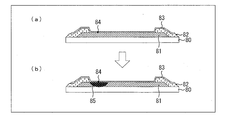
- FIGS. 8 (a) and 8 (b) are diagrams showing a connection terminal portion when copper is used as a wiring material.
- reference numeral 80 denotes a substrate made of glass or the like, and a wiring layer 81 made of copper (Cu) is formed on the substrate 80.
- a base layer such as titanium (Ti), titanium alloy, molybdenum (Mo), or molybdenum alloy is formed, and a Cu layer is formed thereon.
- This Cu wiring layer extends to the display area in which the TFT and the like are formed, and is connected to the TFT and the like formed in the display area.
- the wiring layer 81 is covered with an insulating layer 82, but a portion of the insulating layer 82 is removed and exposed at an area constituting the connection terminal for electrical connection with an external circuit or the like.
- the transparent electrode material 83 is covered. Since the transparent electrode material 83 such as ITO in the connection portion can be a film formed simultaneously with the formation of the pixel electrode in the display portion, a special process for forming the transparent electrode material 83 in the connection terminal portion can be used. Is not necessary.
- the transparent electrode material 83 such as ITO is formed without defects, but if there is a defect such as the pinhole 84 as shown in FIG. Or the like enters the wiring layer 81 made of Cu, and a corroded portion 85 shown in FIG. 8B is formed. In the worst case, the corroded portion 85 spreads over the entire wiring layer 81 and the wiring layer 81 is disconnected.
- the transparent electrode material 83 such as ITO is formed at the same time as the pixel electrode formation, and it is necessary to keep the light transmittance in the pixel electrode portion at a certain value or more, so it should be thickened without darkness. I can't.
- TCP Transmission Carrier Package
- Patent Document 1 describes a technique for preventing a terminal portion from being corroded by moisture in the air.
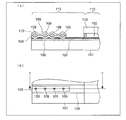
- 9 (a) and 9 (b) and FIG. 10 are diagrams each showing a terminal portion for external connection described in Patent Document 1.
- FIG. 9A is a cross-sectional view taken along the line (nn) in FIG. 9B
- FIG. 9B is a plan view of FIG. 9A.
- FIG. 10 is a diagram showing a configuration when a TCP (Tape Carrier Package) 104 is connected to the terminal portion.
- TCP Transmission Carrier Package
- reference numerals 101 and 103 denote a pair of substrates.
- the substrate 101 is configured as, for example, a matrix array substrate on which switching elements are formed, and the substrate 103 is formed with a color filter or the like. It is configured as a counter board. Wiring layers such as gate wirings and signal wirings are formed on the substrate 101, and these wiring layers are connected to the metal wiring 106 and reach the connection terminals 105 formed in the peripheral region 113 outside the display region 112. Has been pulled out.
- the connection terminal 105 is formed as follows. First, the insulator 107 on the lead metal wiring 106 is removed by a photolithography technique to form a predetermined pattern having a plurality of contact holes, and a part of the metal wiring 106 is exposed. Next, a first conductive film 108 is deposited. Thus, the metal wiring 106 and the first conductive film 108 are electrically connected through the plurality of contact holes. Subsequently, an insulator 109 is formed on the first conductive film 108 so as to cover each contact hole from above, corresponding to each of the plurality of contact holes. After that, a second conductive film 110 is formed over the first conductive film 108 and the insulator 109.
- connection terminal 105 shown in FIGS. 9A and 9B the “contact hole portion exposing the lead-out metal wiring 106 from the insulator 107” is capped by the insulator 109. Thus, moisture can be prevented from entering the connecting portion between the first conductive film 106 and the first conductive film 108.
- FIG. 10 shows a state in which a TCP (Tape Carrier Package) 104 is connected to the connection terminal 105.
- a TCP Transmission Carrier Package
- an anisotropic conductive adhesive in which conductive particles are dispersed in a thermosetting resin. 111 is used.
- FIG. 10 the same members as those in FIGS. 9A and 9B are assigned the same reference numerals, and detailed description thereof will be omitted.
- Japanese Patent Publication Japanese Patent Laid-Open No. 2005-321707 (published on November 17, 2005)”
- the present invention has been made in view of the above-mentioned problems of the prior art, and even when a highly conductive thin film having relatively poor moisture resistance such as copper (Cu) is used, it depends on moisture in the air. It is an object to provide a connection terminal with a low risk of disconnection and to provide a display device using the connection terminal.
- a highly conductive thin film having relatively poor moisture resistance such as copper (Cu)
- a connection terminal is a display device having a lower layer wiring for driving a transparent pixel electrode and an upper layer wiring formed on the lower layer wiring through an insulating layer.
- connection terminal is a three-layer structure of the lower layer wiring, the upper layer wiring, and the transparent conductive thin film, the risk of disconnection can be reduced and a highly reliable connection terminal can be provided.
- connection terminal As described above, in the connection terminal according to the invention of the present application, the outside of the substrate of the display device having the lower layer wiring for driving the transparent pixel electrode and the upper layer wiring formed on the lower layer wiring through the insulating layer.
- the lower layer wiring and the upper layer wiring are connected to each other by a transparent conductive thin film forming the transparent pixel electrode.
- connection terminal part which concerns on Example 1 of this invention. It is a figure for demonstrating the manufacturing method of the connecting terminal which concerns on Example 1 of this invention. It is a figure for demonstrating the structure of the connecting terminal which concerns on Example 2 of this invention, and the manufacturing method of this connecting terminal. It is a figure for demonstrating the structure of the connecting terminal which concerns on Example 3 of this invention, and the manufacturing method of this connecting terminal. It is a figure for demonstrating the structure of the connection terminal which concerns on Example 4 of this invention. It is a figure for demonstrating the structure of the active matrix substrate in a display area, and the manufacturing method of this matrix substrate.
- Embodiment 1 of the present invention will be described based on FIG. 1, FIG. 2 and FIG.
- FIG. 1 is a diagram for explaining a connection terminal and a liquid crystal display device using the connection terminal according to the present invention.
- 1A is a cross-sectional view taken along the line segment (ii) in FIG. 1C, the line segment (gg) in FIG. 1B, and FIG. 1A is a cross-sectional view taken along a line segment (f-f) in FIG. 1A and a line segment (hh) in FIG. 1C, and FIG. 1C is a plan view of a connection terminal portion.
- FIG. 1D is a diagram for explaining the effect of the present invention
- FIG. 1E is a diagram showing a state where TCP is connected to the connection terminal portion according to the present invention. .
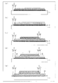
- FIG. 2 is a diagram for explaining a connection terminal and a method of manufacturing a liquid crystal display device using the connection terminal according to the present invention.
- FIG. 6 is a diagram for explaining a manufacturing method of an active element, for example, a TFT formed in a display region (active area) inside the liquid crystal display device.
- an active element for example, a TFT formed in a display region (active area) inside the liquid crystal display device.
- reference numeral 1 denotes a first substrate made of glass or the like, and a first wiring 2 (lower layer) is formed on the substrate 1. Wiring) is formed.
- the substrate 1 is roughly divided into a connection terminal 20 portion and a display region 21 portion.
- An active element such as a TFT is formed on the substrate 1 in the display region 21. Therefore, the first substrate 1 is used as an active matrix substrate in a display device such as a liquid crystal display device. It is.
- the substrate 1 is electrically connected to the outside through the connection terminals 20.
- a second wiring 6 (upper layer wiring) is further formed on the first wiring 2 via the insulating layer 3.
- Both the wiring 2 and the wiring 6 may be Cu wirings having relatively low water resistance. Details will be described later with reference to FIG. 2, and the wiring 2 and the wiring 6 are respectively composed of a lower layer wiring made of Ti or the like and an upper layer wiring made of Cu on the upper side in order to improve adhesion and barrier properties to the substrate or the like.
- a two-layer structure is preferable. In addition, it is not necessarily restricted to this structure.
- Each of the wiring 2 and the wiring 6 may have a laminated structure of copper or a copper alloy and titanium, a titanium compound, molybdenum, or a molybdenum compound.
- the wiring 2 is used as a scanning wiring for supplying a scanning signal to the active element. That is, the wiring 2 is a wiring for driving the pixel electrode (transparent pixel electrode).
- the wiring 6 is used as a signal wiring for supplying an image signal to the pixel electrode through the active element.
- the protective layer 8 is a protective layer deposited after the wiring 6 is formed. As will be described in detail later with reference to FIG. 2, the protective layer 8 is applied to the entire connection terminal portion including the wiring 6, and thereafter, both end portions 15 and 16 of the wiring 2, the central portion 17 of the wiring 6, and the display area. The portions including the end portions 11 of the 21 are removed by photolithography and etching techniques. As a result, the surface of the wiring 2 or the wiring 6 is exposed in these portions. The openings provided in the protective layer 8 and the insulating layer 3 provided at the end portion 11 have a role as contact holes between the first wiring 2 and the second wiring 6. Called.
- Reference numeral 10 denotes a transparent conductive thin film made of ITO or the like.
- the transparent conductive thin film 10 includes “an exposed portion of the wiring 2 at both ends 15 and 16 of the wiring 2” and “a central portion 17 of the wiring 6. In the “exposed portion”, it is deposited so as to be in direct contact with the wiring 2 and the wiring 6, and is further deposited in the contact hole 11 so as to be in direct contact with the exposed portion of the wiring 2 and the wiring 6. .
- the wiring 2 and the wiring 6 are electrically connected to each other via the transparent conductive thin film 10 such as ITO.
- the connection terminal 20 portion the first wiring 2 and the second wiring 6 are connected. It can be seen that the wiring 6 is connected in parallel.
- the transparent conductive thin film 10 is deposited and formed at the same time as the pixel electrode is deposited in the display area. Further, by adopting such a configuration, the number of connection points between the wiring 2 and the wiring 6 can be increased, and the risk of disconnection at the connection terminal 20 portion can be further reduced.
- the end of the wiring 6 may be exposed.
- the transparent conductive thin film 10 is in direct contact with the wiring 2 and the wiring 6 at “the exposed portion of the wiring 2 at both ends 15 and 16 of the wiring 2” and “the exposed portion of the end of the wiring 6”. Will be attached. Also with such a configuration, the number of connection points between the wiring 2 and the wiring 6 can be increased, and the risk of disconnection at the connection terminal 20 portion can be further reduced.
- Reference numeral 13 denotes a second substrate (color filter substrate) on which a color filter or the like is formed in the display area 21, and the substrate 13 is disposed to face the substrate 1 and is placed on the substrate 1 via the sealing member 12. Bonded and fixed. Note that liquid crystal is sealed in the space 14 between the substrate 1 and the substrate 13.
- the transparent conductive thin film 10 made of ITO or the like is normally deposited at the same time as the pixel electrode formed in the display area 21 and is formed so thick as to ensure transparency in the pixel electrode portion. I can't. Therefore, it is difficult to completely eliminate the risk of defects such as pinholes in the transparent conductive thin film 10.
- the first wiring 2 is corroded by moisture in the air.
- Reference numeral 23 denotes this corroded portion. If the corroded portion 23 is enlarged and the entire wiring 2 in the end portion 15 is corroded, the electrical connection between the wiring 2 and the wiring 6 through this portion is “disconnected”.
- connection terminal 20 according to the present invention, the electrical connection between the wiring 2 and the wiring 6 through the transparent conductive thin film 10 is still in the end 16 portion and the contact hole 11 portion which are the other end of the wiring 2. Interconnected state is maintained. Then, power supply to the active elements and the like provided in the display area 21 is ensured through the first wiring 2. In one connection terminal portion, the probability that two or more pinholes are generated in the transparent conductive thin film 10 is extremely low, and the probability that the electrical connection between the wiring 2 and the wiring 6 is “disconnected” is extremely low. Therefore, it can be seen that such a connection terminal has a highly reliable connection terminal structure.
- (E) in FIG. 1 shows a state of connection by TCP to the connection terminal 20 portion.
- reference numeral 24 denotes a TCP having an electrode 25 for connection, which is adhered to the transparent conductive thin film 10 at the central portion 17 by an anisotropic conductive adhesive 26.
- the contact hole 11 is provided in the display area 21 (inside the seal surface), but may be provided on the connection terminal 20 portion side. Although it is less prone to cause corrosion of Cu due to moisture when it is provided in the display area 21, the connection terminal of the present invention has sufficient reliability.
- connection terminal of Example 1 of the present application is formed simultaneously with the formation of an active element, for example, a TFT in the display region. Therefore, first, a method for forming active elements in the display region will be described with reference to FIGS. 6A and 6B, and then a method for manufacturing the connection terminal shown in Embodiment 1 will be described with reference to FIGS. 6 and 2, the same number is assigned to the same member, so that the connection terminal of Example 1 is formed simultaneously with the TFT by comparing FIG. 6 and FIG. Can be understood well.
- an active element for example, a TFT in the display region. Therefore, first, a method for forming active elements in the display region will be described with reference to FIGS. 6A and 6B, and then a method for manufacturing the connection terminal shown in Embodiment 1 will be described with reference to FIGS. 6 and 2, the same number is assigned to the same member, so that the connection terminal of Example 1 is formed simultaneously with the TFT by comparing FIG. 6 and FIG. Can be understood well.
- FIG. 6 show the steps of manufacturing an active element in the order of steps.
- a first substrate 1 made of glass or the like is prepared, a Ti film is formed thereon, and a Cu film is further formed thereon.
- the lower Ti film is deposited to 20 to 150 nm, and the upper Cu film is deposited to about 200 to 500 nm.
- the two-layer film composed of the Ti film and the Cu film is patterned by photolithography, wet etching, and resist peeling cleaning to form the first wiring 2 composed of the first lower layer wiring 2b and the first upper layer wiring 2a. To do.
- the first wiring 2 functions as a scanning wiring that supplies a scanning signal to the TFT. (Refer to FIG. 6A).
- An insulating layer 3 is deposited on the substrate 1 on which the first wiring 2 is formed (see FIG. 6B), and further, an amorphous layer that becomes a channel layer 4 and an electrode contact layer 5 on the insulating layer 3.
- a Si layer is deposited. Specifically, by CVD, an SiNx layer having a thickness of 200 to 500 nm as an insulating film 3, an amorphous Si layer having a thickness of 30 to 300 nm as a channel layer, and an electrode contact layer 5 doped with n-type impurities at a high concentration. After forming n + amorphous Si having a thickness of 20 to 150 nm, the electrode contact layer and the channel layer are patterned by photolithography, dry etching, and resist peeling cleaning. (See FIG. 6B).
- a two-layer film composed of a Ti film and a Cu film is formed again on the insulating layer 3 and the electrode contact layer 5, and etching processing for forming a TFT is performed.
- a signal composed of a Cu / Ti film is formed by depositing a lower Ti film of 20 to 150 nm and an upper Cu film of 200 to 500 nm by sputtering and then patterning the deposited film by photolithography, wet etching, and resist peeling cleaning.
- a wiring 6 and a drain wiring 7 are formed.
- n + amorphous Si is removed in the channel portion 30 corresponding to the substantially central portion of the electrode contact layer 5 until the channel layer 4 of the channel portion 30 is reached by dry etching. (See (c) of FIG. 6).
- the signal wiring 6 is composed of a lower layer wiring 6b made of a Ti film and an upper layer wiring 6a made of a Cu film.
- the drain wiring 7 is composed of a lower layer drain wiring 7b made of a Ti film and an upper layer drain wiring 7a made of a Cu film.
- a protective layer 8 and an interlayer insulating film 9 are formed on the signal wiring 6 and the drain wiring 7 (see FIG. 6D).
- a SiNx film is deposited to a thickness of 100 to 700 nm by a CVD method, and then a photosensitive interlayer insulating film material is applied and patterned by photolithography, and then the protective layer 8 and the insulating layer 3 are patterned by dry etching.
- the interlayer insulating film material remains on the substrate as it is patterned because it does not peel off like a resist.
- a transparent conductive thin film 10 such as ITO is formed on the interlayer insulating film 9 and further patterned into a predetermined shape by a photolithography technique to form a pixel electrode.
- a transparent conductive thin film 10 such as ITO is formed on the interlayer insulating film 9 and further patterned into a predetermined shape by a photolithography technique to form a pixel electrode.
- an ITO film is deposited by sputtering to a thickness of 50 to 200 nm, and then patterned by photolithography, wet etching, and resist peeling cleaning to form a pixel electrode made of the ITO film.
- the first substrate on which a plurality of active elements are formed in a matrix is called an active matrix substrate. (See (e) of FIG. 6).
- the Ti film and the Cu film deposited in (c) of FIG. 6 are patterned into a predetermined shape to form the signal wiring 6 and the drain wiring 7. It will be pulled out to the connection terminal 20 side.
- connection terminal of Example 1 With reference to FIG. 2, the manufacturing method of the connection terminal of Example 1 is demonstrated. Since the connection terminals are formed at the same time when the first substrate (active matrix substrate) described with reference to FIG. 6 is manufactured, the deposition method, film thickness, patterning method, and the like of each layer are omitted. The same applies to Examples 2 to 4.
- a Ti film (first lower layer wiring 2b) is formed on a first substrate 1 made of glass or the like, a Cu film (first upper layer wiring 2a) is further formed thereon, and these Ti films are further formed.
- the Cu film is patterned into a predetermined shape to form a first wiring 2 having a two-layer structure. As already described, this is performed simultaneously with the formation of the first wiring 2 in FIG. 6 (see FIG. 2A).
- an insulating layer 3 is formed thereon, and a channel layer 4 and an electrode contact layer 5 are formed on the insulating layer 3.
- the channel layer 4 and the electrode contact are formed.
- Layer 5 has been removed by etching. (See (b) in FIG. 2).
- a two-layer film composed of a Ti film and a Cu film is formed again on the insulating layer 3 and patterned into a predetermined shape by a photolithography technique to form a second wiring 6.
- the second wiring 6 is formed simultaneously with the formation of the second lower layer wiring 6b, the second upper layer wiring 6a, the second lower layer wiring 7b, and the second upper layer wiring 7a described with reference to FIG. It is what is done. (See (c) in FIG. 2).
- the protective layer 8 is deposited on the entire surface, and further, both end portions 15 and 16 of the first wiring 2 and the central portion 17 of the second wiring 6 are exposed as shown in FIG. Further, an interlayer insulating film 9 is formed on the entire surface, but this interlayer insulating film 9 is completely removed at the connection terminal portion. Thereafter, simultaneously with the formation of the pixel electrode in the display region, a transparent conductive thin film 10 such as ITO is deposited and patterned into a predetermined shape. (See (e) in FIG. 2).
- connection terminal in which the first wiring 2 and the second wiring 6 are connected to each other by the transparent conductive thin film 10 is formed.
- connection terminal 20 of the present embodiment can be realized as a configuration without the interlayer insulating film 9, and conversely, can be realized as a configuration.
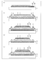
- Example 2 of the present invention will be described with reference to FIG.
- the channel layer 4 and the electrode contact layer 5 removed in the first embodiment are left in the connection terminal portion.
- the rest of the configuration is the same as that of the connection terminal of the first embodiment, and will be briefly described below.
- the first wiring 2 is formed on the glass substrate 1, and then, as shown in FIG. 3B, the insulating layer 3 having a predetermined shape is formed by photolithography. A channel layer 4 and an electrode contact layer 5 are formed, and contact holes reaching the insulating layer 3 are formed in the both end portions 15 and 16 of the first wiring 2 with respect to the channel layer 4 and the electrode contact layer 5.
- a second wiring 6 having a predetermined shape is formed on the electrode contact layer 5, and further, as shown in FIG.
- the insulating layer 3 and the like are removed by an etching technique so that the contact hole formed in 16 reaches the first wiring 2.
- a transparent electrode thin film 10 such as ITO is deposited, and finally, the transparent electrode thin film 10 is patterned into a predetermined shape. Will be.
- Example 2 the contact layer 5 and the channel layer 4 are also used as a part of the wiring layer, which is advantageous in that a wiring having a necessary conductivity is obtained.
- the configuration in the display area is not shown, the configuration is the same as that in FIG.
- connection terminal 20 of the present embodiment can be realized as a configuration without the interlayer insulating film 9, and conversely, can be realized as a configuration.
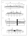
- Example 3 of the present invention will be described with reference to (a), (b), (c) and (d) of FIG. 4A is a sectional view taken along a line (kk) in FIG. 4C, which will be described later, and FIG. 4B is a line (j) in FIG. 4A.
- FIG. 4J is a cross-sectional view taken along the line (mm) in FIG. 4C and FIG. 4C
- FIG. 4C is a plan view of the connection terminal portion.
- FIG. 4D is a diagram for explaining the effect of the present invention.
- the connection terminal portion of the third embodiment is formed at the same time as the formation of the active elements such as TFTs in the display region described with reference to FIG. Are assigned the same number.
- the first wiring 2 is formed on the glass substrate 1, and the second wiring 6 is further formed through the insulating layer 3. Is formed.
- the first wiring 2 is divided into three wirings in the connection terminal 20 portion, and the second wiring The wiring 6 is arranged in a state of being divided into two at the portion between the divided first wirings 2. That is, both the first wiring 2 and the second wiring 6 have a structure branched into a plurality of lines.
- the number of divisions is not limited to the number shown in FIG.
- each of the first wiring 2 divided into three and each of the second wiring 6 divided into two are transparent conductive materials such as ITO.
- the thin films 10 are connected to each other.
- the first wiring 2 and the second wiring 6 are connected to each other through the contact hole 11.
- Reference numeral 8 denotes a protective layer.
- the contact hole 11 is provided in the display region 21, it may be provided on the connection terminal 20 portion side as in the case of the first embodiment.
- FIG. 4 (d) shows a case where a part of the transparent conductive thin film 10 such as ITO is defective and corroded by moisture in the air, but the central wiring 2 is disconnected due to corrosion.
- electrical connection to the display area is achieved by the wirings 2 on both sides. The probability that all the wirings 2 are corroded is considerably low. Therefore, according to the third embodiment of the present invention, a highly reliable connection terminal can be provided.
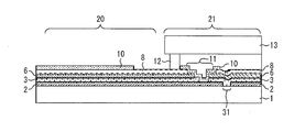
- Example 4 of the present invention will be described with reference to FIG.
- the first to third embodiments are the configuration of the connection terminal for the first wiring 2, while the fourth embodiment is the configuration of the connection terminal for the second wiring 6.
- FIG. 5 is a drawing corresponding to FIG. 1A, and the same members as those in FIG. 1A are given the same numbers. Further, although a plan view corresponding to FIG. 1C is not shown, only the display area 21 is different as described below, and the connection terminal 20 has the same configuration.
- reference numeral 1 denotes a substrate made of glass or the like, on which a first wiring 2 and a second wiring 6 are provided via an insulating layer 3.
- the first wiring 2 and the second wiring 6 are electrically connected to each other by the transparent conductive thin film 10.
- the contact hole 11 is connected to the second wiring 6 on the connection terminal 20 side and is also connected to the second wiring 6 on the display area 21 side.
- the first wiring 2 is disconnected at the region 31.
- 8 is a protective layer
- 12 is a sealing member
- 13 is a 2nd board
- FIG. 5 does not show a cross-sectional view of the connection terminal 20 side of the fourth embodiment, but the same configuration as that of the first to third embodiments can be adopted.
- the fourth embodiment it is possible to provide a highly reliable connection terminal for drawing the second wiring in the display area, that is, the signal wiring of the active matrix substrate out of the display area.
- the first wiring 2 and the second wiring 6 have been described as a Cu / Ti two-layer structure, but Mo or Mo alloy is used instead of the lower Ti layer. Etc. can be used. Further, although amorphous Si is used for the channel layer, an oxide semiconductor such as ⁇ c-Si, ZnO, or IGZO may be used.
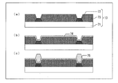
- FIG. 7 is a diagram for explaining the structure of the second substrate and the manufacturing method thereof.
- a liquid crystal display device will be described below as an example.
- the second substrate 13 is a substrate on which a color filter is formed, and is also referred to as a color filter substrate.
- a photosensitive material is used, and a black matrix 72 and red, green, and blue color filters 73 are formed by a photolithography technique.
- a counter electrode 74 is formed as shown in FIG.
- an ITO film is deposited by sputtering to a thickness of 50 to 200 nm and then patterned by photolithography and wet etching.
- a photo spacer 75 is formed.
- a photosensitive material is used and formed by photolithography.
- an alignment film made of polyimide is formed on the first substrate and the second substrate formed by each process by a printing method, and the first substrate and the second substrate are subjected to sealant printing and liquid crystal dropping. After that, the individual display devices are created by dividing by bonding and dicing.
- connection between the lower layer wiring and the upper layer wiring by the transparent conductive thin film is performed at an end portion of the lower layer wiring and a central portion of the upper layer wiring. It is characterized by what is being done.
- the number of connection points between the lower layer wiring and the upper layer wiring can be increased, and the risk of disconnection in the connection terminal portion can be further reduced.
- connection between the lower layer wiring and the upper layer wiring by the transparent conductive thin film is performed by connecting a central portion of the lower layer wiring and an end portion of the upper layer wiring. It is characterized by what is being done in.
- the number of connection points between the lower layer wiring and the upper layer wiring can be increased, and the risk of disconnection in the connection terminal portion can be further reduced.
- connection terminal in order to solve the above problems, in the connection terminal according to still another invention of the present application, the connection between the lower layer wiring and the upper layer wiring by the transparent conductive thin film is performed through a contact hole. Yes.
- each of the upper layer wiring and the lower layer wiring is connected to the external terminal connection electrode (ITO), even if one of the wirings is disconnected, it is conductive on the other, so that disconnection as a terminal can be prevented.
- ITO external terminal connection electrode
- connection terminal is characterized in that the contact hole is placed inside a seal surface of a display device.
- connection terminal in order to solve the above-described problem, in the connection terminal according to still another invention of the present application, at least one of the upper layer wiring and the lower layer wiring has a structure branched into a plurality of lines in the connection terminal portion. It is said.
- the number of connection points between the upper layer wiring and the lower layer wiring by the transparent conductive thin film is increased, and the reliability at the connection terminal portion can be further increased.
- the upper layer wiring and the lower layer wiring are a laminated structure of copper or a copper alloy and titanium, a titanium compound, molybdenum, or a molybdenum compound.
- the transparent conductive thin film is ITO.
- connection terminal portion since copper or copper alloy having high conductivity is used, it is possible to provide a highly reliable connection terminal corresponding to miniaturization of the connection terminal portion.
- connection terminal according to still another invention of the present application is characterized in that the display terminal includes any one of the connection terminals described above.
- a display device having a highly reliable connection terminal can be provided.
- connection terminal is characterized in that the substrate of the display device is an active matrix substrate.
- a display device is characterized in that the display device is a liquid crystal display device.
- the present invention can be used for a connection terminal for external connection such as a display device represented by a liquid crystal display device.
Landscapes
- Physics & Mathematics (AREA)
- Nonlinear Science (AREA)
- Mathematical Physics (AREA)
- Chemical & Material Sciences (AREA)
- Crystallography & Structural Chemistry (AREA)
- General Physics & Mathematics (AREA)
- Optics & Photonics (AREA)
- Engineering & Computer Science (AREA)
- Microelectronics & Electronic Packaging (AREA)
- Devices For Indicating Variable Information By Combining Individual Elements (AREA)
- Liquid Crystal (AREA)
- Electroluminescent Light Sources (AREA)
Abstract
Description
2 第1の配線(下層配線)
3 絶縁層
4 チャネル層
5 電極コンタクト層
6 第2の配線(上層配線)
7 ドレイン電極
8 保護層
9 層間絶縁層
10 透明導電薄膜
11 コンタクトホール
12 封止部材
13 第2の基板
20 接続端子
21 表示領域
24 TCP
25 電極
26 異方性導電接着剤
Claims (10)
- 透明画素電極を駆動するための下層配線と、前記下層配線上に絶縁層を介して形成された上層配線とを有する表示装置の基板における外部への接続端子であって、
前記下層配線と前記上層配線は、前記透明画素電極を形成する透明導電薄膜によって相互に接続されていることを特徴とする接続端子。 - 前記透明導電薄膜による前記下層配線と前記上層配線との接続は、前記下層配線の端部と前記上層配線の中央部において行われていることを特徴とする請求項1に記載の接続端子。
- 前記透明導電薄膜による前記下層配線と前記上層配線との接続は、前記下層配線の中央部と前記上層配線の端部とにおいて行われていることを特徴とする請求項1に記載の接続端子。
- 前記透明導電薄膜による前記下層配線と前記上層配線との接続は、コンタクトホールを介して行われていることを特徴とする請求項1から3のいずれか1項に記載の接続端子。
- 前記コンタクトホールは、表示装置のシール面の内側に置かれていることを特徴とする請求項4に記載の接続端子。
- 前記上層配線及び前記下層配線の少なくとも一方は、接続端子部分において複数本に枝分かれされた構造とされていることを特徴とする請求項1から5のいずれか一項に記載の接続端子。
- 前記上層配線及び前記下層配線は、
銅または銅合金と、
チタン、チタン化合物、モリブデン、またはモリブデン化合物と、
の積層構造であり、
前記透明導電薄膜はITOであることを特徴とする請求項1から6のいずれか一項に記載の接続端子。 - 請求項1から7のいずれか1項に記載の接続端子を有する表示装置。
- 前記表示装置の基板は、アクティブマトリックス基板であることを特徴とする請求項8に記載の表示装置。
- 前記表示装置は液晶表示装置であることを特徴とする請求項9に記載の表示装置。
Priority Applications (6)
| Application Number | Priority Date | Filing Date | Title |
|---|---|---|---|
| CN200980156141XA CN102308330A (zh) | 2009-02-10 | 2009-12-01 | 连接端子和具备该连接端子的显示装置 |
| JP2010550417A JP5154665B2 (ja) | 2009-02-10 | 2009-12-01 | 接続端子及び該接続端子を備えた表示装置 |
| RU2011133359/07A RU2492598C2 (ru) | 2009-02-10 | 2009-12-01 | Соединительный вывод и устройство отображения с соединительным выводом |
| BRPI0924282A BRPI0924282A2 (pt) | 2009-02-10 | 2009-12-01 | terminal de conexão e aparelho de vídeo incluindo os mesmos |
| EP09840044A EP2398008A4 (en) | 2009-02-10 | 2009-12-01 | CONNECTION TERMINAL AND DISPLAY DEVICE WITH CONNECTION TERMINAL |
| US13/144,259 US20110279766A1 (en) | 2009-02-10 | 2009-12-01 | Connecting terminal and display apparatus including same |
Applications Claiming Priority (2)
| Application Number | Priority Date | Filing Date | Title |
|---|---|---|---|
| JP2009-028829 | 2009-02-10 | ||
| JP2009028829 | 2009-02-10 |
Publications (1)
| Publication Number | Publication Date |
|---|---|
| WO2010092725A1 true WO2010092725A1 (ja) | 2010-08-19 |
Family
ID=42561574
Family Applications (1)
| Application Number | Title | Priority Date | Filing Date |
|---|---|---|---|
| PCT/JP2009/070194 Ceased WO2010092725A1 (ja) | 2009-02-10 | 2009-12-01 | 接続端子及び該接続端子を備えた表示装置 |
Country Status (7)
| Country | Link |
|---|---|
| US (1) | US20110279766A1 (ja) |
| EP (1) | EP2398008A4 (ja) |
| JP (2) | JP5154665B2 (ja) |
| CN (1) | CN102308330A (ja) |
| BR (1) | BRPI0924282A2 (ja) |
| RU (1) | RU2492598C2 (ja) |
| WO (1) | WO2010092725A1 (ja) |
Cited By (1)
| Publication number | Priority date | Publication date | Assignee | Title |
|---|---|---|---|---|
| JP2014021472A (ja) * | 2012-07-24 | 2014-02-03 | Mitsubishi Electric Corp | 表示パネルおよび表示装置 |
Families Citing this family (4)
| Publication number | Priority date | Publication date | Assignee | Title |
|---|---|---|---|---|
| US9112181B2 (en) * | 2012-02-07 | 2015-08-18 | Panasonic Corporation | Composite substrate, manufacturing method of the same and organic electroluminescence device |
| KR102115174B1 (ko) * | 2012-06-18 | 2020-05-27 | 삼성디스플레이 주식회사 | 표시 패널 |
| JP6358535B2 (ja) * | 2013-04-26 | 2018-07-18 | パナソニックIpマネジメント株式会社 | 配線板間接続構造、および配線板間接続方法 |
| JP6324098B2 (ja) * | 2014-02-06 | 2018-05-16 | 株式会社ジャパンディスプレイ | 表示装置及びその製造方法 |
Citations (7)
| Publication number | Priority date | Publication date | Assignee | Title |
|---|---|---|---|---|
| JP2002176056A (ja) * | 2000-12-06 | 2002-06-21 | Fujitsu Ltd | 外部接続端子及びそれを備えた液晶表示装置及びその製造方法 |
| WO2002065434A1 (fr) * | 2001-02-16 | 2002-08-22 | Seiko Epson Corporation | Dispositif electro-optique et materiel electronique |
| JP2005217087A (ja) * | 2004-01-29 | 2005-08-11 | Chi Mei Electronics Corp | 銅拡散を防止可能なアレイ基板及びその製造方法 |
| JP2005321707A (ja) | 2004-05-11 | 2005-11-17 | Nec Lcd Technologies Ltd | 液晶表示装置 |
| JP2007139867A (ja) * | 2005-11-15 | 2007-06-07 | Mitsubishi Electric Corp | アクティブマトリックス基板 |
| JP2008015226A (ja) * | 2006-07-06 | 2008-01-24 | Epson Imaging Devices Corp | 電気光学装置、電気光学装置の製造方法及び電子機器 |
| JP2009004518A (ja) * | 2007-06-20 | 2009-01-08 | Kobe Steel Ltd | 薄膜トランジスタ基板、および表示デバイス |
Family Cites Families (13)
| Publication number | Priority date | Publication date | Assignee | Title |
|---|---|---|---|---|
| JP2790002B2 (ja) * | 1993-06-14 | 1998-08-27 | カシオ計算機株式会社 | 薄膜トランジスタパネル |
| US5982470A (en) * | 1996-08-29 | 1999-11-09 | Sharp Kabushiki Kaisha | Liquid crystal display device having dummy electrodes with interleave ratio same on all sides |
| JP3302894B2 (ja) * | 1996-11-25 | 2002-07-15 | 株式会社東芝 | 液晶表示装置 |
| NO304956B1 (no) * | 1997-07-22 | 1999-03-08 | Opticom As | Elektrodeanordning uten og med et funksjonselement, samt en elektrodeinnretning dannet av elektrodeanordninger med funksjonselement og anvendelser derav |
| JPH11109889A (ja) * | 1997-10-03 | 1999-04-23 | Sanyo Electric Co Ltd | 表示装置 |
| US6049365A (en) * | 1998-05-07 | 2000-04-11 | Mitsubishi Denki Kabushiki Kaisha | Liquid crystal displaying apparatus with a converter not exposed to liquid crystal |
| KR100672622B1 (ko) * | 2000-07-26 | 2007-01-23 | 엘지.필립스 엘시디 주식회사 | 액정표시장치의 패드 및 그 제조방법 |
| NO316632B1 (no) * | 2001-11-16 | 2004-03-15 | Thin Film Electronics Asa | Matriseadresserbart optoelektronisk apparat og elektrodeanordning i samme |
| US7408611B2 (en) * | 2003-07-29 | 2008-08-05 | Tpo Hong Kong Holding Limited | Electronic apparatus with a wiring terminal |
| US20060138349A1 (en) * | 2004-12-27 | 2006-06-29 | Asml Netherlands B.V. | Lithographic apparatus and device manufacturing method |
| JP4543385B2 (ja) * | 2005-03-15 | 2010-09-15 | 日本電気株式会社 | 液晶表示装置の製造方法 |
| EP3614442A3 (en) * | 2005-09-29 | 2020-03-25 | Semiconductor Energy Laboratory Co., Ltd. | Semiconductor device having oxide semiconductor layer and manufactoring method thereof |
| JP5196870B2 (ja) * | 2007-05-23 | 2013-05-15 | キヤノン株式会社 | 酸化物半導体を用いた電子素子及びその製造方法 |
-
2009
- 2009-12-01 WO PCT/JP2009/070194 patent/WO2010092725A1/ja not_active Ceased
- 2009-12-01 RU RU2011133359/07A patent/RU2492598C2/ru not_active IP Right Cessation
- 2009-12-01 EP EP09840044A patent/EP2398008A4/en not_active Withdrawn
- 2009-12-01 US US13/144,259 patent/US20110279766A1/en not_active Abandoned
- 2009-12-01 BR BRPI0924282A patent/BRPI0924282A2/pt not_active IP Right Cessation
- 2009-12-01 CN CN200980156141XA patent/CN102308330A/zh active Pending
- 2009-12-01 JP JP2010550417A patent/JP5154665B2/ja not_active Expired - Fee Related
-
2012
- 2012-07-31 JP JP2012170476A patent/JP5290456B2/ja not_active Expired - Fee Related
Patent Citations (7)
| Publication number | Priority date | Publication date | Assignee | Title |
|---|---|---|---|---|
| JP2002176056A (ja) * | 2000-12-06 | 2002-06-21 | Fujitsu Ltd | 外部接続端子及びそれを備えた液晶表示装置及びその製造方法 |
| WO2002065434A1 (fr) * | 2001-02-16 | 2002-08-22 | Seiko Epson Corporation | Dispositif electro-optique et materiel electronique |
| JP2005217087A (ja) * | 2004-01-29 | 2005-08-11 | Chi Mei Electronics Corp | 銅拡散を防止可能なアレイ基板及びその製造方法 |
| JP2005321707A (ja) | 2004-05-11 | 2005-11-17 | Nec Lcd Technologies Ltd | 液晶表示装置 |
| JP2007139867A (ja) * | 2005-11-15 | 2007-06-07 | Mitsubishi Electric Corp | アクティブマトリックス基板 |
| JP2008015226A (ja) * | 2006-07-06 | 2008-01-24 | Epson Imaging Devices Corp | 電気光学装置、電気光学装置の製造方法及び電子機器 |
| JP2009004518A (ja) * | 2007-06-20 | 2009-01-08 | Kobe Steel Ltd | 薄膜トランジスタ基板、および表示デバイス |
Non-Patent Citations (1)
| Title |
|---|
| See also references of EP2398008A4 * |
Cited By (1)
| Publication number | Priority date | Publication date | Assignee | Title |
|---|---|---|---|---|
| JP2014021472A (ja) * | 2012-07-24 | 2014-02-03 | Mitsubishi Electric Corp | 表示パネルおよび表示装置 |
Also Published As
| Publication number | Publication date |
|---|---|
| RU2492598C2 (ru) | 2013-09-10 |
| US20110279766A1 (en) | 2011-11-17 |
| JP2012215907A (ja) | 2012-11-08 |
| JP5290456B2 (ja) | 2013-09-18 |
| RU2011133359A (ru) | 2013-02-20 |
| EP2398008A1 (en) | 2011-12-21 |
| EP2398008A4 (en) | 2012-09-19 |
| CN102308330A (zh) | 2012-01-04 |
| JP5154665B2 (ja) | 2013-02-27 |
| BRPI0924282A2 (pt) | 2016-01-26 |
| JPWO2010092725A1 (ja) | 2012-08-16 |
Similar Documents
| Publication | Publication Date | Title |
|---|---|---|
| CN102473369B (zh) | 配线基板及其制造方法、显示面板以及显示装置 | |
| US9087752B2 (en) | Semiconductor device, display device, and method for manufacturing semiconductor device and display device | |
| CN113937236B (zh) | 显示基板及其制备方法、显示装置 | |
| US20140147966A1 (en) | Semiconductor device, display device, and production method for semiconductor device and display device | |
| CN103460270B (zh) | 有源矩阵基板、显示装置和有源矩阵基板的制造方法 | |
| JP4142029B2 (ja) | 電気光学装置および電子機器 | |
| CN104423112A (zh) | 液晶显示装置及其制造方法 | |
| CN100472306C (zh) | 显示装置用基板、其制造方法及显示装置 | |
| CN110890386B (zh) | 薄膜晶体管基板、液晶显示装置及有机电致发光显示装置 | |
| US20150287799A1 (en) | Semiconductor device, display panel, and semiconductor device manufacturing method | |
| KR20130000430A (ko) | 액티브 매트릭스 기판 및 표시패널 | |
| WO2011132376A1 (ja) | 薄膜トランジスタ基板 | |
| CN103026398B (zh) | 基板及其制造方法、显示装置 | |
| JP5290456B2 (ja) | 接続端子及び該接続端子を備えた表示装置 | |
| KR101357480B1 (ko) | 박막 트랜지스터 기판 및 이를 구비한 표시장치 그리고 박막 트랜지스터 기판의 제조방법 | |
| KR20090077117A (ko) | 표시 기판 및 이의 제조 방법 | |
| CN101464573B (zh) | 液晶显示设备及其制造方法 | |
| KR20170081070A (ko) | 수평 전계형 액정 표시장치 및 그 제조방법 | |
| WO2011125268A1 (ja) | 液晶表示パネル | |
| JP2005266683A (ja) | 実装構造体、電気光学装置および電子機器 | |
| KR20160092423A (ko) | 컬러필터 어레이 기판 및 그 제조방법과 이를 포함하는 액정표시장치 및 그 제조방법 | |
| WO2013076940A1 (ja) | アクティブマトリクス基板及び液晶表示装置 |
Legal Events
| Date | Code | Title | Description |
|---|---|---|---|
| WWE | Wipo information: entry into national phase |
Ref document number: 200980156141.X Country of ref document: CN |
|
| 121 | Ep: the epo has been informed by wipo that ep was designated in this application |
Ref document number: 09840044 Country of ref document: EP Kind code of ref document: A1 |
|
| ENP | Entry into the national phase |
Ref document number: 2010550417 Country of ref document: JP Kind code of ref document: A |
|
| WWE | Wipo information: entry into national phase |
Ref document number: 13144259 Country of ref document: US |
|
| WWE | Wipo information: entry into national phase |
Ref document number: 5170/CHENP/2011 Country of ref document: IN |
|
| WWE | Wipo information: entry into national phase |
Ref document number: 2009840044 Country of ref document: EP |
|
| WWE | Wipo information: entry into national phase |
Ref document number: 2011133359 Country of ref document: RU |
|
| NENP | Non-entry into the national phase |
Ref country code: DE |
|
| REG | Reference to national code |
Ref country code: BR Ref legal event code: B01A Ref document number: PI0924282 Country of ref document: BR |
|
| ENP | Entry into the national phase |
Ref document number: PI0924282 Country of ref document: BR Kind code of ref document: A2 Effective date: 20110808 |