WO2010093041A1 - Procédé de production d'une feuille multicouche formant barrière contre les gaz - Google Patents
Procédé de production d'une feuille multicouche formant barrière contre les gaz Download PDFInfo
- Publication number
- WO2010093041A1 WO2010093041A1 PCT/JP2010/052219 JP2010052219W WO2010093041A1 WO 2010093041 A1 WO2010093041 A1 WO 2010093041A1 JP 2010052219 W JP2010052219 W JP 2010052219W WO 2010093041 A1 WO2010093041 A1 WO 2010093041A1
- Authority
- WO
- WIPO (PCT)
- Prior art keywords
- film
- thin film
- gas barrier
- resin
- plasma cvd
- Prior art date
- Legal status (The legal status is an assumption and is not a legal conclusion. Google has not performed a legal analysis and makes no representation as to the accuracy of the status listed.)
- Ceased
Links
Images
Classifications
-
- C—CHEMISTRY; METALLURGY
- C09—DYES; PAINTS; POLISHES; NATURAL RESINS; ADHESIVES; COMPOSITIONS NOT OTHERWISE PROVIDED FOR; APPLICATIONS OF MATERIALS NOT OTHERWISE PROVIDED FOR
- C09D—COATING COMPOSITIONS, e.g. PAINTS, VARNISHES OR LACQUERS; FILLING PASTES; CHEMICAL PAINT OR INK REMOVERS; INKS; CORRECTING FLUIDS; WOODSTAINS; PASTES OR SOLIDS FOR COLOURING OR PRINTING; USE OF MATERIALS THEREFOR
- C09D5/00—Coating compositions, e.g. paints, varnishes or lacquers, characterised by their physical nature or the effects produced; Filling pastes
-
- C—CHEMISTRY; METALLURGY
- C23—COATING METALLIC MATERIAL; COATING MATERIAL WITH METALLIC MATERIAL; CHEMICAL SURFACE TREATMENT; DIFFUSION TREATMENT OF METALLIC MATERIAL; COATING BY VACUUM EVAPORATION, BY SPUTTERING, BY ION IMPLANTATION OR BY CHEMICAL VAPOUR DEPOSITION, IN GENERAL; INHIBITING CORROSION OF METALLIC MATERIAL OR INCRUSTATION IN GENERAL
- C23C—COATING METALLIC MATERIAL; COATING MATERIAL WITH METALLIC MATERIAL; SURFACE TREATMENT OF METALLIC MATERIAL BY DIFFUSION INTO THE SURFACE, BY CHEMICAL CONVERSION OR SUBSTITUTION; COATING BY VACUUM EVAPORATION, BY SPUTTERING, BY ION IMPLANTATION OR BY CHEMICAL VAPOUR DEPOSITION, IN GENERAL
- C23C14/00—Coating by vacuum evaporation, by sputtering or by ion implantation of the coating forming material
- C23C14/06—Coating by vacuum evaporation, by sputtering or by ion implantation of the coating forming material characterised by the coating material
- C23C14/08—Oxides
-
- B—PERFORMING OPERATIONS; TRANSPORTING
- B32—LAYERED PRODUCTS
- B32B—LAYERED PRODUCTS, i.e. PRODUCTS BUILT-UP OF STRATA OF FLAT OR NON-FLAT, e.g. CELLULAR OR HONEYCOMB, FORM
- B32B9/00—Layered products comprising a layer of a particular substance not covered by groups B32B11/00 - B32B29/00
-
- C—CHEMISTRY; METALLURGY
- C23—COATING METALLIC MATERIAL; COATING MATERIAL WITH METALLIC MATERIAL; CHEMICAL SURFACE TREATMENT; DIFFUSION TREATMENT OF METALLIC MATERIAL; COATING BY VACUUM EVAPORATION, BY SPUTTERING, BY ION IMPLANTATION OR BY CHEMICAL VAPOUR DEPOSITION, IN GENERAL; INHIBITING CORROSION OF METALLIC MATERIAL OR INCRUSTATION IN GENERAL
- C23C—COATING METALLIC MATERIAL; COATING MATERIAL WITH METALLIC MATERIAL; SURFACE TREATMENT OF METALLIC MATERIAL BY DIFFUSION INTO THE SURFACE, BY CHEMICAL CONVERSION OR SUBSTITUTION; COATING BY VACUUM EVAPORATION, BY SPUTTERING, BY ION IMPLANTATION OR BY CHEMICAL VAPOUR DEPOSITION, IN GENERAL
- C23C14/00—Coating by vacuum evaporation, by sputtering or by ion implantation of the coating forming material
- C23C14/06—Coating by vacuum evaporation, by sputtering or by ion implantation of the coating forming material characterised by the coating material
- C23C14/10—Glass or silica
-
- C—CHEMISTRY; METALLURGY
- C23—COATING METALLIC MATERIAL; COATING MATERIAL WITH METALLIC MATERIAL; CHEMICAL SURFACE TREATMENT; DIFFUSION TREATMENT OF METALLIC MATERIAL; COATING BY VACUUM EVAPORATION, BY SPUTTERING, BY ION IMPLANTATION OR BY CHEMICAL VAPOUR DEPOSITION, IN GENERAL; INHIBITING CORROSION OF METALLIC MATERIAL OR INCRUSTATION IN GENERAL
- C23C—COATING METALLIC MATERIAL; COATING MATERIAL WITH METALLIC MATERIAL; SURFACE TREATMENT OF METALLIC MATERIAL BY DIFFUSION INTO THE SURFACE, BY CHEMICAL CONVERSION OR SUBSTITUTION; COATING BY VACUUM EVAPORATION, BY SPUTTERING, BY ION IMPLANTATION OR BY CHEMICAL VAPOUR DEPOSITION, IN GENERAL
- C23C14/00—Coating by vacuum evaporation, by sputtering or by ion implantation of the coating forming material
- C23C14/22—Coating by vacuum evaporation, by sputtering or by ion implantation of the coating forming material characterised by the process of coating
- C23C14/56—Apparatus specially adapted for continuous coating; Arrangements for maintaining the vacuum, e.g. vacuum locks
-
- C—CHEMISTRY; METALLURGY
- C23—COATING METALLIC MATERIAL; COATING MATERIAL WITH METALLIC MATERIAL; CHEMICAL SURFACE TREATMENT; DIFFUSION TREATMENT OF METALLIC MATERIAL; COATING BY VACUUM EVAPORATION, BY SPUTTERING, BY ION IMPLANTATION OR BY CHEMICAL VAPOUR DEPOSITION, IN GENERAL; INHIBITING CORROSION OF METALLIC MATERIAL OR INCRUSTATION IN GENERAL
- C23C—COATING METALLIC MATERIAL; COATING MATERIAL WITH METALLIC MATERIAL; SURFACE TREATMENT OF METALLIC MATERIAL BY DIFFUSION INTO THE SURFACE, BY CHEMICAL CONVERSION OR SUBSTITUTION; COATING BY VACUUM EVAPORATION, BY SPUTTERING, BY ION IMPLANTATION OR BY CHEMICAL VAPOUR DEPOSITION, IN GENERAL
- C23C14/00—Coating by vacuum evaporation, by sputtering or by ion implantation of the coating forming material
- C23C14/22—Coating by vacuum evaporation, by sputtering or by ion implantation of the coating forming material characterised by the process of coating
- C23C14/56—Apparatus specially adapted for continuous coating; Arrangements for maintaining the vacuum, e.g. vacuum locks
- C23C14/562—Apparatus specially adapted for continuous coating; Arrangements for maintaining the vacuum, e.g. vacuum locks for coating elongated substrates
-
- C—CHEMISTRY; METALLURGY
- C23—COATING METALLIC MATERIAL; COATING MATERIAL WITH METALLIC MATERIAL; CHEMICAL SURFACE TREATMENT; DIFFUSION TREATMENT OF METALLIC MATERIAL; COATING BY VACUUM EVAPORATION, BY SPUTTERING, BY ION IMPLANTATION OR BY CHEMICAL VAPOUR DEPOSITION, IN GENERAL; INHIBITING CORROSION OF METALLIC MATERIAL OR INCRUSTATION IN GENERAL
- C23C—COATING METALLIC MATERIAL; COATING MATERIAL WITH METALLIC MATERIAL; SURFACE TREATMENT OF METALLIC MATERIAL BY DIFFUSION INTO THE SURFACE, BY CHEMICAL CONVERSION OR SUBSTITUTION; COATING BY VACUUM EVAPORATION, BY SPUTTERING, BY ION IMPLANTATION OR BY CHEMICAL VAPOUR DEPOSITION, IN GENERAL
- C23C16/00—Chemical coating by decomposition of gaseous compounds, without leaving reaction products of surface material in the coating, i.e. chemical vapour deposition [CVD] processes
- C23C16/22—Chemical coating by decomposition of gaseous compounds, without leaving reaction products of surface material in the coating, i.e. chemical vapour deposition [CVD] processes characterised by the deposition of inorganic material, other than metallic material
- C23C16/30—Deposition of compounds, mixtures or solid solutions, e.g. borides, carbides, nitrides
- C23C16/40—Oxides
-
- C—CHEMISTRY; METALLURGY
- C23—COATING METALLIC MATERIAL; COATING MATERIAL WITH METALLIC MATERIAL; CHEMICAL SURFACE TREATMENT; DIFFUSION TREATMENT OF METALLIC MATERIAL; COATING BY VACUUM EVAPORATION, BY SPUTTERING, BY ION IMPLANTATION OR BY CHEMICAL VAPOUR DEPOSITION, IN GENERAL; INHIBITING CORROSION OF METALLIC MATERIAL OR INCRUSTATION IN GENERAL
- C23C—COATING METALLIC MATERIAL; COATING MATERIAL WITH METALLIC MATERIAL; SURFACE TREATMENT OF METALLIC MATERIAL BY DIFFUSION INTO THE SURFACE, BY CHEMICAL CONVERSION OR SUBSTITUTION; COATING BY VACUUM EVAPORATION, BY SPUTTERING, BY ION IMPLANTATION OR BY CHEMICAL VAPOUR DEPOSITION, IN GENERAL
- C23C16/00—Chemical coating by decomposition of gaseous compounds, without leaving reaction products of surface material in the coating, i.e. chemical vapour deposition [CVD] processes
- C23C16/22—Chemical coating by decomposition of gaseous compounds, without leaving reaction products of surface material in the coating, i.e. chemical vapour deposition [CVD] processes characterised by the deposition of inorganic material, other than metallic material
- C23C16/30—Deposition of compounds, mixtures or solid solutions, e.g. borides, carbides, nitrides
- C23C16/40—Oxides
- C23C16/401—Oxides containing silicon
-
- C—CHEMISTRY; METALLURGY
- C23—COATING METALLIC MATERIAL; COATING MATERIAL WITH METALLIC MATERIAL; CHEMICAL SURFACE TREATMENT; DIFFUSION TREATMENT OF METALLIC MATERIAL; COATING BY VACUUM EVAPORATION, BY SPUTTERING, BY ION IMPLANTATION OR BY CHEMICAL VAPOUR DEPOSITION, IN GENERAL; INHIBITING CORROSION OF METALLIC MATERIAL OR INCRUSTATION IN GENERAL
- C23C—COATING METALLIC MATERIAL; COATING MATERIAL WITH METALLIC MATERIAL; SURFACE TREATMENT OF METALLIC MATERIAL BY DIFFUSION INTO THE SURFACE, BY CHEMICAL CONVERSION OR SUBSTITUTION; COATING BY VACUUM EVAPORATION, BY SPUTTERING, BY ION IMPLANTATION OR BY CHEMICAL VAPOUR DEPOSITION, IN GENERAL
- C23C16/00—Chemical coating by decomposition of gaseous compounds, without leaving reaction products of surface material in the coating, i.e. chemical vapour deposition [CVD] processes
- C23C16/44—Chemical coating by decomposition of gaseous compounds, without leaving reaction products of surface material in the coating, i.e. chemical vapour deposition [CVD] processes characterised by the method of coating
- C23C16/54—Apparatus specially adapted for continuous coating
- C23C16/545—Apparatus specially adapted for continuous coating for coating elongated substrates
-
- C—CHEMISTRY; METALLURGY
- C23—COATING METALLIC MATERIAL; COATING MATERIAL WITH METALLIC MATERIAL; CHEMICAL SURFACE TREATMENT; DIFFUSION TREATMENT OF METALLIC MATERIAL; COATING BY VACUUM EVAPORATION, BY SPUTTERING, BY ION IMPLANTATION OR BY CHEMICAL VAPOUR DEPOSITION, IN GENERAL; INHIBITING CORROSION OF METALLIC MATERIAL OR INCRUSTATION IN GENERAL
- C23C—COATING METALLIC MATERIAL; COATING MATERIAL WITH METALLIC MATERIAL; SURFACE TREATMENT OF METALLIC MATERIAL BY DIFFUSION INTO THE SURFACE, BY CHEMICAL CONVERSION OR SUBSTITUTION; COATING BY VACUUM EVAPORATION, BY SPUTTERING, BY ION IMPLANTATION OR BY CHEMICAL VAPOUR DEPOSITION, IN GENERAL
- C23C28/00—Coating for obtaining at least two superposed coatings either by methods not provided for in a single one of groups C23C2/00 - C23C26/00 or by combinations of methods provided for in subclasses C23C and C25C or C25D
-
- B—PERFORMING OPERATIONS; TRANSPORTING
- B05—SPRAYING OR ATOMISING IN GENERAL; APPLYING FLUENT MATERIALS TO SURFACES, IN GENERAL
- B05D—PROCESSES FOR APPLYING FLUENT MATERIALS TO SURFACES, IN GENERAL
- B05D1/00—Processes for applying liquids or other fluent materials
- B05D1/62—Plasma-deposition of organic layers
-
- B—PERFORMING OPERATIONS; TRANSPORTING
- B05—SPRAYING OR ATOMISING IN GENERAL; APPLYING FLUENT MATERIALS TO SURFACES, IN GENERAL
- B05D—PROCESSES FOR APPLYING FLUENT MATERIALS TO SURFACES, IN GENERAL
- B05D2252/00—Sheets
- B05D2252/02—Sheets of indefinite length
-
- B—PERFORMING OPERATIONS; TRANSPORTING
- B05—SPRAYING OR ATOMISING IN GENERAL; APPLYING FLUENT MATERIALS TO SURFACES, IN GENERAL
- B05D—PROCESSES FOR APPLYING FLUENT MATERIALS TO SURFACES, IN GENERAL
- B05D2350/00—Pretreatment of the substrate
- B05D2350/60—Adding a layer before coating
-
- B—PERFORMING OPERATIONS; TRANSPORTING
- B05—SPRAYING OR ATOMISING IN GENERAL; APPLYING FLUENT MATERIALS TO SURFACES, IN GENERAL
- B05D—PROCESSES FOR APPLYING FLUENT MATERIALS TO SURFACES, IN GENERAL
- B05D7/00—Processes, other than flocking, specially adapted for applying liquids or other fluent materials to particular surfaces or for applying particular liquids or other fluent materials
- B05D7/50—Multilayers
- B05D7/56—Three layers or more
Definitions
- the present invention relates to a laminated film having excellent gas barrier properties and a method for producing the same.
- a gas barrier plastic film in which a plastic film is used as a base material and an inorganic thin film is formed on the surface thereof is used for packaging articles that require blocking of various gases such as water vapor and oxygen, such as food, industrial products, and pharmaceuticals.
- various gases such as water vapor and oxygen
- the gas barrier plastic film has recently attracted attention as a new application as a transparent conductive sheet used in liquid crystal display elements, solar cells, electromagnetic wave shields, touch panels, EL substrates, color filters, and the like. ing.
- the gas barrier plastic film formed with such an inorganic thin film several improvements have been studied for various purposes. For example, from the viewpoint of transparency and gas barrier property, a metal oxide is applied to the plastic film.
- a gas barrier film (see Patent Document 1) having a total light transmittance of 85% or more formed by sequentially laminating a physical layer / resin / metal oxide layer is also used to prevent and suppress damage to the metal oxide.
- a barrier film (see Patent Document 2) in which a metal oxide layer and an organic layer are alternately laminated on a transparent plastic film is disclosed.
- Patent Document 3 has a gas barrier film formed of silicon nitride and / or silicon oxynitride on at least one surface of a base material, and has a configuration of base material / resin layer / barrier layer / resin layer / barrier layer and the like.
- a barrier film is disclosed.
- Patent Document 4 shows that a film containing a metal oxide having a high carbon content acts as a stress relaxation layer, thereby preventing the entire film from cracking or delamination. Shows a gas barrier laminate film composed of base film / inorganic thin film / anchor coat layer / inorganic thin film.
- Patent Document 6 discloses an improvement in barrier properties by a laminated vapor deposition film layer in which two or more silicon oxide vapor deposition films are laminated on a substrate by repeating the vapor deposition process twice or more. Discloses that wet heat resistance and gas barrier properties are improved by a gas barrier laminate having an inorganic oxide layer and a silicon oxynitride carbide layer or silicon oxide carbide layer in this order on a base film. Further, Patent Document 8 has a gas barrier thin film made of a metal or a metal compound formed by physical vapor deposition on a substrate, and a polyimide formed by vapor deposition synthesis between the substrate and the gas barrier thin film.
- Patent Document 9 discloses that an inorganic compound film is provided on a base material made of a polymer resin by a vacuum deposition method, and an organic compound is formed by a chemical vapor deposition method. Manufacturing a gas barrier material that is distributed in the thickness direction to form an organic / inorganic composite film.
- these target properties are improved to some extent in these films, for example, the gas barrier properties, the adhesion strength between the constituent layers of the laminated film and the productivity are still insufficient, and the improvement is desired. It was.
- the problem to be solved by the present invention is to produce a laminated film having good adhesion, showing high gas barrier properties immediately after production, and having excellent adhesion strength between constituent layers while maintaining excellent gas barrier properties. It is in providing the gas barrier laminated film obtained by this method and this manufacturing method.
- the present invention (1) (1) A step of forming an inorganic thin film on at least one surface of a substrate film by a vacuum deposition method, (2) A step of forming a thin film by a plasma CVD method on the inorganic thin film formed in step (1) And (3) a method for producing a gas barrier laminate film comprising a step of forming an inorganic thin film by a vacuum deposition method on the thin film formed in step (2), wherein the steps (1) and (3)
- Each of the above steps (1) and (3) is preferably carried out under a pressure of 1 ⁇ 10 ⁇ 7 to 1 Pa and step (2) under a pressure of 1 ⁇ 10 ⁇ 3 to 1 ⁇ 10 2 Pa.
- Laminated film About.
- the present invention is a method for producing a laminated film having good productivity, showing high gas barrier properties immediately after production, and having excellent adhesion strength between the constituent layers of the laminated film, while maintaining excellent gas barrier properties, and A gas barrier laminate film obtained by the production method is provided.
- Step (1) is a step of forming an inorganic thin film on at least one surface of the base film by a vacuum deposition method.
- the base film of the gas barrier laminate film of the present invention is preferably a thermoplastic polymer film, and the raw material thereof can be used without particular limitation as long as it can be used for ordinary packaging materials.
- polyolefins such as homopolymers or copolymers such as ethylene, propylene and butene, amorphous polyolefins such as cyclic polyolefin, polyesters such as polyethylene terephthalate and polyethylene-2,6-naphthalate, nylon 6, nylon 66, nylon 12, polyamide such as copolymer nylon, polyvinyl alcohol, ethylene-vinyl acetate copolymer partial hydrolyzate (EVOH), polyimide, polyetherimide, polysulfone, polyethersulfone, polyetheretherketone, polycarbonate, Examples include polyvinyl butyral, polyarylate, fluororesin, acrylate resin, and biodegradable resin.
- polyester, polyamide, polyolefin, and biodegradable resin are preferable from the viewpoint of film strength and cost.
- the base film is a known additive such as an antistatic agent, a light blocking agent, an ultraviolet absorber, a plasticizer, a lubricant, a filler, a colorant, a stabilizer, a lubricant, a crosslinking agent, an antiblocking agent, An antioxidant etc. can be contained.
- thermoplastic polymer film as the substrate film is formed by using the above raw materials, but when used as a substrate, it may be unstretched or stretched. Good. Moreover, you may laminate
- a base film can be produced by a conventionally known method. For example, a raw material resin is melted by an extruder, extruded by an annular die or a T die, and rapidly cooled to be oriented substantially amorphously. No unstretched film can be produced. The unstretched film is subjected to a known method such as uniaxial stretching, tenter sequential biaxial stretching, tenter simultaneous biaxial stretching, tubular simultaneous biaxial stretching, or the like. A film stretched in at least a uniaxial direction can be produced by stretching in a direction (horizontal axis) perpendicular thereto.
- the thickness of the base film is usually 5 to 500 ⁇ m, preferably 10 to 200 ⁇ m, depending on its use from the viewpoint of mechanical strength, flexibility, transparency, etc. as the base material of the gas barrier laminate film of the present invention.
- a sheet-like material selected in a range and having a large thickness is also included.
- Inorganic material constituting the inorganic thin film formed by vacuum vapor deposition on at least one surface of the substrate film includes silicon, aluminum, magnesium, zinc, tin, nickel, titanium, hydrocarbon, etc. Alternatively, these oxides, carbides, nitrides or mixtures thereof may be mentioned. From the viewpoint of gas barrier properties, silicon oxide, aluminum oxide, hydrocarbons (for example, hydrocarbons such as diamond-like carbon) are mainly used. Substance). In particular, silicon oxide and aluminum oxide are preferable in that high gas barrier properties can be stably maintained. Although the said inorganic substance may be used individually by 1 type, you may use it in combination of 2 or more type.
- the inorganic thin film For the formation of the inorganic thin film, a vacuum deposition method is used in that a uniform thin film having high gas barrier properties can be obtained.
- the thickness of the inorganic thin film is generally 0.1 to 500 nm, but is preferably 0.5 to 100 nm, more preferably 1 to 50 nm from the viewpoint of gas barrier properties and film productivity.
- the inorganic thin film is formed under reduced pressure in order to form a dense thin film, preferably while transporting the film.
- the pressure for forming the inorganic thin film is from 1 ⁇ 10 ⁇ 7 to 1 Pa, preferably from 1 ⁇ 10 ⁇ 6 to 1 ⁇ 10 ⁇ 1 Pa, from the viewpoints of vacuum exhaust capability and barrier properties. If it is in the said range, sufficient gas-barrier property will be acquired, and it will be excellent also in transparency, without generating a crack and peeling in an inorganic thin film.
- Step (2) is a step of forming a thin film by plasma CVD on the inorganic thin film formed in step (1).
- defects such as defects generated in the inorganic thin film obtained in the step (1) are sealed, and it is considered that gas barrier properties and interlayer adhesion are improved.
- Thin films formed by the plasma CVD method include thin films obtained by polymerizing organic compounds and converting them to resins, inorganic substances such as metals, metal oxides and metal nitrides obtained by plasma decomposition of organic compounds, inorganic oxidation And a thin film made of at least one selected from the group consisting of oxides and inorganic nitrides.
- a known organic compound can be used as an organic compound serving as a raw material component for plasma polymerization, but an organic compound having at least one unsaturated bond or cyclic structure in the molecule is preferable from the viewpoint of film formation speed.
- monomers or oligomers such as (meth) acrylic compounds, epoxy compounds, oxetane compounds and the like can be preferably used, but particularly preferred include acrylic compounds, methacrylic compounds, epoxy compounds, etc.
- the main component is an acrylic compound.
- Resins that form thin films by plasma CVD include polyester resins, urethane resins, acrylic resins, epoxy resins, cellulose resins, silicon resins, vinyl alcohol resins, polyvinyl alcohol resins, and ethylene vinyl alcohol resins. , Vinyl modified resins, isocyanate group-containing resins, carbodiimide resins, alkoxyl group-containing resins, oxazoline group-containing resins, modified styrene resins, modified silicon resins, alkyl titanate resins, polyparaxylylene resins, etc. Or it can use in combination of 2 or more types.
- polyester resins from the viewpoint of gas barrier properties, among the above resins, polyester resins, urethane resins, acrylic resins, epoxy resins, cellulose resins, silicon resins, isocyanate group-containing resins, polyparaxylylene systems It is preferable to use at least one resin selected from the group consisting of resins and copolymers thereof. Of these, acrylic resins are preferred.
- polyester resin either saturated or unsaturated polyester can be used.
- dicarboxylic acid component of the saturated polyester include aromatic dicarboxylic acids such as terephthalic acid, isophthalic acid, and 2,5-naphthalenedicarboxylic acid, aliphatic dicarboxylic acids such as adipic acid, azelaic acid, and sebacic acid, and oxybenzoic acid. Oxycarboxylic acids and their ester-forming derivatives.
- glycol component examples include aliphatic glycols such as ethylene glycol, 1,4-butanediol, diethylene glycol, and triethylene glycol, alicyclic glycols such as 1,4-cyclohexanedimethanol, and aromatics such as p-xylylenediol.
- the above-mentioned saturated polyester has a linear structure, but can also be made into a branched polyester using a trivalent or higher ester-forming component.
- an unsaturated polyester having a copolymerizable unsaturated group in a resin skeleton obtained by reacting a raw material component containing a polymerizable unsaturated group with another raw material component.
- An unsaturated polyester having a copolymerizable unsaturated group in a resin skeleton obtained by reacting a raw material component containing a polymerizable unsaturated group with another raw material component.
- an unsaturated polyester obtained by adding a vinyl monomer having a functional group reactive with a functional group such as a carboxyl group and a vinyl group to a saturated polyester.
- Examples of the vinyl monomer include compounds having an epoxy group and a vinyl group such as glycidyl methacrylate, compounds having an alkoxysilanol group and a vinyl group such as vinylmethoxysilane and methacryloxyethyltrimethoxysilane, maleic anhydride, tetrahydro
- Examples thereof include compounds having an acid anhydride group and a vinyl group such as phthalic anhydride, and compounds having an isocyanate group and a vinyl group such as 2-hydroxypropyl methacrylate-hexamethylene diisocyanate adduct.
- the urethane-based resin is a resin produced by reacting a polyhydroxy compound and a polyisocyanate compound according to a conventional method.
- the polyhydroxy compound (2) include polyethylene glycol, polypropylene glycol, polyethylene / propylene glycol, polytetramethylene glycol, hexamethylene glycol, tetramethylene glycol, 1,5-pentanediol, diethylene glycol, triethylene glycol, Examples include polycaprolactone, polyhexamethylene adipate, polyhexamethylene sebacate, polytetramethylene adipate, polytetramethylene sebacate, trimethylolpropane, trimethylolethane, pentaerythritol, glycerin and the like.
- polyisocyanate compound examples include hexamethylene diisocyanate, diphenylmethane diisocyanate, tolylene diisocyanate, isophorone diisocyanate, an adduct of tolylene diisocyanate and trimethylolpropane, an adduct of hexamethylene diisocyanate and trimethylolethane, and the like.
- the useful (meth) acrylic compound for forming the acrylic resin is not particularly limited, but specific examples include the following compounds. That is, 2-ethylhexyl acrylate, 2-hydroxypropyl acrylate, glycerol acrylate, tetrahydrofurfuryl acrylate, phenoxyethyl acrylate, nonylphenoxyethyl acrylate, tetrahydrofurfuryloxyethyl acrylate, tetrahydrofurfuryloxyhexanolide acrylate, 1,3- Monofunctional acrylic acid esters such as acrylate of ⁇ -caprolactone adduct of dioxane alcohol, 1,3-dioxolane acrylate, or methacrylic acid esters in which these acrylates are replaced by methacrylates; for example, ethylene glycol diacrylate, triethylene glycol Coal diacrylate, pentaerythritol diacrylate, hydroquinone diacrylate, reso Syn
- Methacrylic acid esters in which salts are replaced with methacrylates for example, trimethylolpropane triacrylate, ditrimethylolpropane tetraacrylate, trimethylolethane triacrylate, pentaerythritol triacrylate, pentaerythritol tetraacrylate, dipentaerythritol tetraacrylate, dipentaerythritol Pentaacrylate, dipentaerythritol hexaacrylate, ⁇ -caprolactone adduct of dipentaerythritol hexaacrylate, pyrogallol triacrylate, propionic acid / dipentaerythritol triacrylate, propionic acid / dipentaerythritol tetraacrylate, hydroxypivalylaldehyde-modified dimethylol Propane triacrylate, etc.
- Epoxy resins include bisphenol A type, bisphenol F type, biphenyl type, novolac type, phenol novolac type, glycidyl ester type epoxy resin, modified aliphatic amine, modified alicyclic amine, modified aromatic amine, ketimine And those obtained by reacting a curing agent such as polyfunctional phenol, imidazole, mercaptan, acid anhydride, and dicyandiamide.
- a curing agent such as polyfunctional phenol, imidazole, mercaptan, acid anhydride, and dicyandiamide.
- an epoxy resin having a glycidylamine moiety derived from metaxylylenediamine an epoxy resin having a glycidylamine moiety derived from 1,3-bis (aminomethyl) cyclohexane, and a glycidyl derived from diaminodiphenylmethane
- Epoxy resin having amine moiety epoxy resin having glycidylamine moiety derived from paraaminophenol, epoxy resin having glycidyl ether moiety derived from bisphenol A, epoxy resin having glycidyl ether moiety derived from bisphenol F, phenol Examples thereof include an epoxy resin having a glycidyl ether moiety derived from novolak, and an epoxy resin having a glycidyl ether moiety derived from resorcinol.
- An epoxy resin having an amine moiety is preferred in terms of gas barrier properties.
- Examples of the epoxy resin curing agent include the following reactive organisms (A) and (B), or reactive organisms (A), (B), and (C).
- A a polyfunctional compound having at least one acyl group that can form an amide group site by reaction with meta-xylenediamine or para-xylenediamine
- B polyamine to form an oligomer
- Monovalent carboxylic acid and / or derivative thereof metaxylylenediamine or paraxylylenediamine, a modified reaction product of epoxy resin or monoglycidyl compound using these as raw materials, alkylene oxide having 2 to 4 carbon atoms Reaction product with polyfunctional compound having at least one acyl group, which can form an amide group site and form an oligomer by reaction with these polyamines.
- Can form oligomers by forming amide groups by reaction with these polyamines examples thereof include a reaction product of a polyfunctional compound having one acyl group with a monovalent carboxylic acid having 1 to 8 carbon atoms and / or a derivative thereof.
- cellulose resin examples include various cellulose derivative resins such as cellulose, nitrocellulose, cellulose acetate, alkali cellulose, hydroxyethyl cellulose, carboxymethyl cellulose, carboxymethyl cellulose sodium, cellulose acetate butyrate, and cellulose acetate.
- cellulose derivative resins such as cellulose, nitrocellulose, cellulose acetate, alkali cellulose, hydroxyethyl cellulose, carboxymethyl cellulose, carboxymethyl cellulose sodium, cellulose acetate butyrate, and cellulose acetate.
- isocyanate group-containing resin examples include hexamethylene-1,6-diisocyanate, dicyclohexylmethane-4,4′-diisocyanate, 3-isocyanatemethyl-3,5,5-trimethylcyclohexylisocyanate, 1,3-bis (isocyanato).
- polyparaxylylene-based resin examples include paraxylylene, polymers thereof such as a chlorine-substituted benzene ring hydrogen, and a fluorine-substituted methyl group hydrogen.
- a diamine compound having a metaxylylene skeleton, a paraxylylene skeleton, or a 1,3-bis (methyl) cyclohexane skeleton such as metaxylylenediamine, paraxylylenediamine, 1,3-bis (aminomethyl) cyclohexane may be used alone.
- good gas barrier properties can be obtained.
- the raw material gas used when forming an organic thin film by the plasma CVD method is an organic compound which is a raw material component of the plasma polymerization, an unsaturated hydrocarbon compound such as acetylene, ethylene or propylene, or a saturated gas such as methane, ethane or propane. Examples thereof include hydrocarbon compounds, aromatic hydrocarbon compounds such as benzene, toluene and xylene.
- the source gas may be used alone or in combination of two or more.
- the source gas may be diluted with a rare gas such as argon (Ar) or helium (He).
- silane coupling agent examples include epoxy group-containing silanes such as ⁇ - (3,4-epoxycyclohexyl) ethyltrimethoxysilane, ⁇ -glycidoxypropylmethyldiethoxylane, and ⁇ -glycidoxypropyltrimethoxysilane.
- silane coupling agent ⁇ -aminopropyltrimethoxysilane, N- ⁇ (aminoethyl) ⁇ -aminopropylmethyljetoxylan, N- ⁇ (aminoethyl) ⁇ -aminopropyltrimethoxylane, N- ⁇ (aminoethyl) ⁇ -Amino group-containing silane coupling agents such as aminopropyltriethoxylane and the like, and mixtures thereof.
- preferred silane coupling agents include ⁇ -glycidoxypropyltrimethoxysilane and ⁇ -aminopropyltrimethoxysilane. These silane coupling agents may be used alone or in combination of two or more.
- the silane coupling agent is preferably contained in a proportion of 0.1 to 80% by mass, more preferably 1 to 50% by mass with respect to the resin forming the plasma CVD thin film.
- the plasma CVD thin film preferably contains a curing agent, and it is preferable to use polyisocyanate as the curing agent.
- polyisocyanate include aliphatic polyisocyanates such as hexamethylene diisocyanate and dicyclohexylmethane diisocyanate, and aromatic polyisocyanates such as xylene diisocyanate, tolylene diisocyanate, diphenylmethane diisocyanate, polymethylene polyphenylene diisocyanate, tolidine diisocyanate, and naphthalene diisocyanate. It is done.
- bifunctional or higher polyisocyanates are preferable from the viewpoint of improving barrier properties.
- the plasma CVD thin film may contain various known additives.
- additives include polyhydric alcohols such as glycerin, ethylene glycol, polyethylene glycol and polypropylene glycol, aqueous epoxy resins, lower alcohols such as methanol, ethanol, normal propanol and isopropanol, ethylene glycol monomethyl ether, propylene glycol monomethyl ether.
- Ethers such as propylene glycol diethyl ether, diethylene glycol monoethyl ether, propylene glycol monoethyl ether, esters such as propylene glycol monoacetate and ethylene glycol monoacetate, antioxidants, weathering stabilizers, UV absorbers, antistatic agents , Pigments, dyes, antibacterial agents, lubricants, inorganic fillers, antiblocking agents, adhesives and the like.
- a thin film containing at least one selected from inorganic substances such as metals, metal oxides, and metal nitrides, inorganic oxides, inorganic nitrides, etc. gas barrier properties, adhesion properties
- metals such as silicon, titanium, DLC and the like, or alloys of two or more of these, are preferably mentioned, and as the inorganic oxide or inorganic nitride, oxides of the above metals from the viewpoint of gas barrier properties and adhesion , Nitrides and mixtures thereof are preferred.
- the plasma CVD thin film is composed of at least one selected from silicon oxide, silicon nitride, silicon nitride oxide, titanium oxide, and diamond-like carbon (hereinafter referred to as “DLC”) from the above viewpoint. Is more preferable. These are preferably those obtained by plasma decomposition of an organic compound.
- the thin film formed by the plasma CVD method contains carbon characteristically from its raw materials and chemical reaction, and its content is usually 10 atomic% or more as measured by XPS (X-ray photoelectron spectroscopy). is there.
- a compound such as a silicon compound can be used in a gas, liquid, or solid state at normal temperature and pressure.
- gas it can be introduced into the discharge space as it is, but in the case of liquid or solid, it is used after being vaporized by means such as heating, bubbling, decompression or ultrasonic irradiation.
- the solvent may be diluted with a solvent, and an organic solvent such as methanol, ethanol, n-hexane, or a mixed solvent thereof may be used as the solvent.
- silicon compound examples include silane, tetramethoxysilane, tetraethoxysilane, tetra n-propoxysilane, tetraisopropoxysilane, tetra n-butoxysilane, tetrat-butoxysilane, dimethyldimethoxysilane, dimethyldiethoxysilane, and diethyldimethoxy.
- Silane diphenyldimethoxysilane, methyltriethoxysilane, ethyltrimethoxysilane, phenyltriethoxysilane, (3,3,3-trifluoropropyl) trimethoxysilane, hexamethyldisiloxane, bis (dimethylamino) dimethylsilane, bis (Dimethylamino) methylvinylsilane, bis (ethylamino) dimethylsilane, N, O-bis (trimethylsilyl) acetamide, bis (trimethylsilyl) carbodiimide, diethyl Minotrimethylsilane, dimethylaminodimethylsilane, hexamethyldisilazane, hexamethylcyclotrisilazane, heptamethyldisilazane, nonamethyltrisilazane, octamethylcyclotetrasilazane, tetra
- the titanium compound is a titanium inorganic compound or a titanium organic compound.
- titanium inorganic compounds include titanium oxide and titanium chloride.
- titanium organic compounds include titanium alkoxides such as titanium tetrabutoxide, tetranormal butyl titanate, butyl titanate dimer, tetra (2-ethylhexyl) titanate, tetramethyl titanate, titanium lactate, titanium acetylacetonate, titanium tetraacetylacetonate, Examples include titanium chelates such as polytitanium acetylacetonate, titanium octylene glycolate, titanium ethyl acetoacetate, and titanium triethanolamate.
- the thin film can be formed by plasma CVD by alternately or simultaneously forming the resin layer and a thin film made of at least one selected from the inorganic substances, inorganic oxides, inorganic nitrides and the like.
- the upper limit of the thickness of the plasma CVD thin film is preferably 5000 nm, more preferably 500 nm, and even more preferably 100 nm.
- the lower limit is 0.1 nm, and preferably 0.5 nm. If the thickness is within the above range, the adhesion and gas barrier properties are good, which is preferable.
- the thickness of the plasma CVD thin film is preferably 0.1 to 5000 nm, more preferably 0.1 to 500 nm, and further preferably 0.1 to 100 nm.
- the pressure at which the plasma CVD thin film is formed is preferably reduced under reduced pressure in order to form a dense thin film.
- the pressure for forming the thin film is from 1 ⁇ 10 ⁇ 3 to 1 ⁇ 10 2 Pa, preferably from 1 ⁇ 10 ⁇ 2 to 10 Pa, from the viewpoint of film formation speed and barrier properties.
- This plasma CVD thin film can be subjected to a crosslinking treatment by electron beam irradiation in order to improve water resistance and durability.
- the raw material compound is evaporated and introduced into a vacuum apparatus as a raw material gas, and direct current (DC) plasma, low frequency plasma, high frequency (RF) plasma, pulse wave plasma, tripolar structure It can be performed by converting into plasma with a low-temperature plasma generator such as plasma, microwave plasma, downstream plasma, columnar plasma, plasma assisted epitaxy or the like. From the viewpoint of plasma stability, a radio frequency (RF) plasma apparatus is more preferable.
- DC direct current
- RF radio frequency
- Step (3) is a step of forming an inorganic thin film on the thin film formed in step (2) by a vacuum deposition method.
- Examples of the vacuum deposition method in step (3) and the inorganic thin film formed thereby include the same as those described in step (1).
- the inorganic thin film formed by the vacuum deposition method in the step (1) or in the steps (1) and (3) is made of SiOx 1 with 1.2 ⁇ x 1 ⁇ 1.9, and in the step (2).
- the thin film formed by the plasma CVD method is formed of SiOx 2 satisfying 1.5 ⁇ x 2 ⁇ 2.5, and forming a thin film within a range of 0.3 ⁇ x 2 ⁇ x 1 ⁇ 1.3. preferable.
- the thin film formed by the plasma CVD method is more oxidized than the inorganic thin film formed by the vacuum vapor deposition method, so that the thin film obtained by the vapor deposition method is effectively sealed.
- the above steps (1) to (3) are continuously performed at a specific pressure under reduced pressure. From the same viewpoint, in the present invention, it is preferable to perform all of the above steps in the same vacuum chamber, preferably while transporting the film. That is, in the present invention, after each step is completed, the pressure in the vacuum chamber is returned to near atmospheric pressure, and the vacuum is not re-executed to perform the post-process, but the film is continuously formed in a vacuum state. Is preferred.
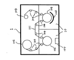
- FIG. 1 is a schematic explanatory view showing an example of a vacuum film forming apparatus for carrying out the manufacturing method of the present invention.
- a vacuum film forming apparatus 1 for producing a gas barrier laminated film enables winding of a web-like substrate film 101 while applying a constant back tension by a torque control means such as a powder clutch.
- the film forming chamber 10 has temperature control film forming drums 105 and 106 for controlling the temperature of the film surface during film formation and forming a film on the film surface, and a vapor deposition heating source 107. , And an electrode 108 for plasma CVD having a shower head for introducing process gas or source gas.
- the apparatus shown in FIG. 1 is an example of a take-up vacuum film forming apparatus, but other batch-type film forming apparatuses can be used in the present invention.
- the base film 101 is unwound from the unwinding shaft 102 and introduced into the film forming chamber 10, and then the film base 101 from the vapor deposition heating source 106 on the temperature-controlled film forming drum 105.
- a deposited film is deposited on the film, and then transported to a temperature-controlled film-forming drum 106.
- a CVD thin film is formed on the deposited film on the base film 101 by using an electrode 108 for plasma CVD. Winding around the take-up shaft 103.
- the unwinding shaft 102 is once performed.
- the film can be repeatedly formed after rewinding, or a CVD thin film is further formed on the film using the plasma CVD electrode 108 when rewinding to the unwinding shaft 102, and then deposited.
- a vapor deposition film can be deposited on the film using the heating source 106.
- step (3) by performing the steps (1) to (3) in the same vacuum chamber, a very good gas barrier property can be expressed.
- the principle is not clear, by forming the plasma CVD thin film in the same vacuum tank as the inorganic thin film formation by vacuum deposition, the minute defects generated in the thin film by the vapor deposition method are uniformly observed, and further, step (3) It is considered that the gas barrier property of the second vapor-deposited layer can be further improved.
- step (2) and step (3) are performed after step (1) is performed.
- step (2) and step (3) can be repeated one or more times.
- the steps (2) and (3) are preferably repeated 1 to 3 times, and more preferably 1 or 2 times.
- the adhesiveness of each layer in the multilayer film of an inorganic thin film can be improved by performing a process (2) and a process (3).
- the gas barrier property can be improved by repeating the steps (2) and (3) at least once, preferably 1 to 3 times.
- the pressure in each of steps (1) and (3) is preferably lower than the pressure in step (2).
- the ratio of the pressure in step (2) to the pressure in each of steps (1) and (3) is preferably 10 to 1 ⁇ 10 7 , more preferably 1 ⁇ 10 2 to 10 6 , and still more preferably 1 ⁇ 10 2 to 1 ⁇ 10 5 .
- the pressure difference between the pressure in each of the steps (1) and (3) and the pressure in the step (2) is 0.001 Pa or more, more preferably 0.01 Pa or more.
- anchor coat layer In the present invention, it is preferable to provide an anchor coat layer by applying an anchor coating agent between the base film and the inorganic thin film in order to improve the adhesion between the base film and the inorganic thin film by vapor deposition.
- the anchor coating agent from the viewpoint of productivity, the same resin as the resin that forms the resin layer as the plasma CVD thin film obtained in the step (2) can be used.
- the thickness of the anchor coat layer provided on the base film is usually 0.1 to 5000 nm, preferably 1 to 2000 nm, more preferably 1 to 1000 nm. If it is in the above range, the slipperiness is good, there is almost no peeling from the base film due to the internal stress of the anchor coat layer itself, and a uniform thickness can be maintained.
- the gas barrier laminate film of the present invention preferably has a protective layer as the uppermost layer on the side where the thin film is formed by the above steps (1) to (3).
- a resin for forming the protective layer both solvent-based and water-based resins can be used. Specifically, polyester resins, urethane resins, acrylic resins, polyvinyl alcohol resins, ethylene Unsaturated carboxylic acid copolymer resin, ethylene vinyl alcohol resin, vinyl modified resin, nitrocellulose resin, silicon resin, isocyanate resin, epoxy resin, oxazoline group-containing resin, modified styrene resin, modified silicon resin, Alkyl titanates can be used alone or in combination of two or more.
- the protective layer one or more kinds of inorganic particles selected from silica sol, alumina sol, particulate inorganic filler, and layered inorganic filler are mixed with the one or more kinds of resins in order to improve barrier properties, wearability, and slipperiness. It is preferable to use a layer made of an inorganic particle-containing resin formed by polymerizing the resin raw material in the presence of the inorganic particles.
- the above aqueous resin is preferable from the viewpoint of improving the gas barrier property of the inorganic thin film. Further, as the aqueous resin, a polyvinyl alcohol resin, an ethylene vinyl alcohol resin, or an ethylene-unsaturated carboxylic acid copolymer resin is preferable. Below, the said resin layer is demonstrated.
- the polyvinyl alcohol resin can be obtained by a known method, and can usually be obtained by saponifying a vinyl acetate polymer.
- a saponification degree of 80% or more can be used, preferably 90% or more, more preferably 95% or more, and particularly preferably 98% or more from the viewpoint of gas barrier properties.
- the average degree of polymerization is usually 500 to 3000, and preferably 500 to 2000 in terms of gas barrier properties and stretchability.
- what copolymerized ethylene in the ratio of 40% or less as polyvinyl alcohol can also be used.
- the aqueous polyvinyl alcohol solution is prepared, for example, by supplying a polyvinyl alcohol resin while stirring in normal temperature water, raising the temperature, and stirring at 80 to 95 ° C. for 30 to 60 minutes.
- Ethylene-unsaturated carboxylic acid copolymer resins include ethylene, acrylic acid, methacrylic acid, ethacrylic acid, fumaric acid, maleic acid, itaconic acid, monomethyl maleate, monoethyl maleate, maleic anhydride, itaconic anhydride, etc. It is a copolymer with an unsaturated carboxylic acid, and among them, a copolymer of ethylene and acrylic acid or methacrylic acid is preferred from the viewpoint of versatility.
- the ethylene-unsaturated carboxylic acid copolymer may contain any other monomer.
- the ethylene component in the ethylene-unsaturated carboxylic acid copolymer is preferably 65 to 90% by mass, more preferably 70 to 85% by mass from the viewpoint of versatility and flexibility, and the unsaturated carboxylic acid component is preferably 10%. Is 35% by mass, more preferably 15-30% by mass.
- the melt flow rate (MFR) at 190 ° C. under a load of 2160 g of the ethylene-unsaturated carboxylic acid copolymer is preferably 30 to 2000 g / 10 minutes, more preferably 60 to 1500 g from the viewpoint of the bending resistance of the film. / 10 minutes.
- the number average molecular weight is preferably in the range of 2000 to 250,000.
- the ethylene-unsaturated carboxylic acid copolymer preferably contains a partially neutralized product from the viewpoints of gas barrier properties, interlayer adhesion, and the like. From the viewpoint of properties, it is preferably 20 to 100%, more preferably 40 to 100%, and particularly preferably 60 to 100%.
- the degree of neutralization can be obtained from the following formula.
- A Number of moles of neutralized carboxyl group in 1 g of partially neutralized ethylene-unsaturated carboxylic acid copolymer
- B Carboxyl group in 1 g of ethylene-unsaturated carboxylic acid copolymer before partial neutralization
- A is (the number of metal ions in the solvent) x (the valence of the metal ions)
- B is partially neutralized with ethylene-unsaturated carboxylic acid. It can be calculated as the number of carboxyl groups in the acid copolymer.
- the ethylene-unsaturated carboxylic acid copolymer may be used as an aqueous liquid comprising the copolymer and an aqueous medium containing ammonia, sodium hydroxide, potassium hydroxide, lithium hydroxide and the like from the viewpoint of gas barrier properties.
- the above aqueous medium is used so that the degree of neutralization is 20 to 100%, more preferably 40 to 100%, based on the total number of moles of carboxyl groups of the ethylene-unsaturated carboxylic acid copolymer. Those are preferably used.
- the protective layer may be composed of one kind of the resin, but may be used in combination of two or more kinds.
- inorganic particles can be added to the protective layer in order to improve barrier properties and adhesion.
- inorganic particle used for this invention For example, all well-known things, such as an inorganic filler, an inorganic layered compound, a metal oxide sol, can be used.
- inorganic fillers include oxides such as silicon, aluminum, magnesium, calcium, potassium, sodium, titanium, zinc, iron, hydroxides, hydrates, carbonates, and mixtures and composites thereof. .
- Examples of the inorganic layered compound include clay minerals typified by kaolinite group, smectite group, mica group and the like, and montmorillonite, hectorite, saponite and the like can be used.
- Examples of the metal oxide sol include metal oxides such as silicon, antimony, zirconium, aluminum, cerium, and titanium, or a mixture thereof. Among them, from the viewpoint of hot water resistance and gas barrier properties, those having a reactive functional group capable of being hydrolytically condensed such as a hydroxy group and an alkoxy group are preferred. In particular, the reactive functional group contains 10 to 100 mol% of silanol groups, Further, those containing 20 to 100 mol% are preferably used.
- silica particles are preferably used as the inorganic particles from the viewpoint of versatility and stability.
- the said inorganic particle may be used by 1 type, it can also be used in combination of 2 or more type.
- the average particle diameter of the inorganic particles is preferably 0.5 nm, more preferably 1 nm, and the upper limit is preferably 2 ⁇ m, in view of hot water resistance and cohesive fracture resistance.
- it is 200 nm, More preferably, it is 100 nm, More preferably, it is 25 nm, More preferably, it is 10 nm, More preferably, it is 5 nm.
- the average particle size is preferably 0.5 to 2 ⁇ m, more preferably 0.5 to 200 nm, more preferably 0.5 to 100 nm, more preferably 0.5 to 25 nm, and more.
- the thickness is preferably 1 to 20 nm, more preferably 1 to 10 nm, still more preferably 1 to 5 nm.
- the thickness of the protective layer is preferably 0.05 to 10 ⁇ m, more preferably 0.1 to 3 ⁇ m, from the viewpoint of printability and workability.
- a known coating method is appropriately adopted as the formation method. For example, any method such as a reverse roll coater, a gravure coater, a rod coater, an air doctor coater, a spray or a coating method using a brush can be used. Moreover, you may immerse a vapor deposition film in the resin liquid for protective layers. After the application, moisture can be evaporated using a known drying method such as hot air drying at a temperature of about 80 to 200 ° C., heat drying such as hot roll drying, or infrared drying. Thereby, a laminated film having a uniform coating layer is obtained.
- the following embodiments can be preferably used from the viewpoint of gas barrier properties and adhesion.
- Base film / AC / inorganic thin film / plasma CVD thin film / inorganic thin film (2) Base film / AC / inorganic thin film / plasma CVD thin film / inorganic thin film / plasma CVD thin film / inorganic thin film (3) Base film / AC / inorganic thin film / plasma CVD thin film / inorganic thin film / plasma CVD thin film / inorganic thin film / plasma CVD thin film / inorganic thin film / plasma CVD thin film / inorganic thin film (4) base film / AC / inorganic thin film / plasma CVD thin film / inorganic thin film / protective layer (5) base Material film / AC / inorganic thin film / plasma CVD thin film / inorganic thin film / plasma CVD thin film / inorganic thin film / protective layer (6) substrate film /
- Base film / inorganic thin film / plasma CVD thin film / inorganic thin film (8) Base film / inorganic thin film / plasma CVD thin film / inorganic thin film / plasma CVD thin film / inorganic thin film (9) Base film / inorganic thin film / plasma CVD thin film / inorganic thin film / plasma CVD thin film / inorganic thin film / AC / inorganic thin film (10) base film / inorganic thin film / plasma CVD thin film / inorganic thin film / protective layer (11) base film / inorganic thin film / plasma CVD thin film / Inorganic thin film / plasma CVD thin film / inorganic thin film / protective layer (12) substrate film / inorganic thin film / plasma CVD thin film / inorganic thin film / plasma CVD thin film / inorganic thin film / plasma CVD thin film / inorganic thin film / protective layer (AC indicates the anchor coat layer.)
- various gas barrier laminate films in which additional constituent layers are further laminated on the above constituent layers as necessary can be used according to applications.
- a gas barrier laminate film in which a plastic film is provided on the inorganic thin film or the protective layer is used for various applications.
- the thickness of the plastic film is usually selected in the range of 5 to 500 ⁇ m, preferably 10 to 200 ⁇ m, depending on the application, from the viewpoints of mechanical strength, flexibility, transparency as a substrate of the laminated structure. .
- the width and length of the film are not particularly limited and can be appropriately selected according to the intended use.
- heat sealing becomes possible and it can be used as various containers.
- heat-sealable resins include known resins such as polyethylene resins, polypropylene resins, ethylene-vinyl acetate copolymers, ionomer resins, acrylic resins, and biodegradable resins.
- the gas barrier laminate film there may be mentioned one in which a print layer is formed on the coated surface of the inorganic thin film or the protective layer, and a heat seal layer is further laminated thereon.
- a printing ink for forming the printing layer aqueous and solvent-based resin-containing printing inks can be used.
- the resin used in the printing ink include acrylic resins, urethane resins, polyester resins, vinyl chloride resins, vinyl acetate copolymer resins, and mixtures thereof.
- antistatic agents for printing inks, antistatic agents, light shielding agents, ultraviolet absorbers, plasticizers, lubricants, fillers, colorants, stabilizers, lubricants, antifoaming agents, crosslinking agents, antiblocking agents, antioxidants, etc.
- plasticizers for printing inks, antistatic agents, light shielding agents, ultraviolet absorbers, plasticizers, lubricants, fillers, colorants, stabilizers, lubricants, antifoaming agents, crosslinking agents, antiblocking agents, antioxidants, etc.
- lubricants for printing inks, antistatic agents, light shielding agents, ultraviolet absorbers, plasticizers, lubricants, fillers, colorants, stabilizers, lubricants, antifoaming agents, crosslinking agents, antiblocking agents, antioxidants, etc.
- a printing method for providing a printing layer can be used.
- Well-known printing methods such as an offset printing method, a gravure printing method, and a screen printing method, can be used.
- a known drying method such as hot air drying, hot roll drying, or infrared drying can be used.
- a plastic film the thing similar to the thermoplastic polymer film as a base film used for the gas barrier laminate film of the present invention can be used.
- paper, polyester resin, polyamide resin or biodegradable resin is preferable from the viewpoint of obtaining sufficient rigidity and strength of the laminate.
- heating is performed from the viewpoints of gas barrier properties, film quality and coating layer quality stabilization, and the like. It is preferable to perform the treatment.
- the conditions for the heat treatment vary depending on the type and thickness of the elements constituting the gas barrier laminated film, but are not particularly limited as long as the necessary temperature and time can be maintained.
- a method of storing in an oven or temperature-controlled room set to the required temperature a method of blowing hot air, a method of heating with an infrared heater, a method of irradiating light with a lamp, or heating directly by contact with a hot roll or hot plate
- a method of imparting a light, a method of irradiating with a microwave, or the like can be used.
- a heating device can be incorporated in a part of a film manufacturing apparatus such as a coater or a slitter, and heating can be performed in the manufacturing process.
- the temperature of the heat treatment is not particularly limited as long as it is a temperature below the melting point of the base material, plastic film, etc. to be used, but it is 60 ° C. or higher because the treatment time necessary for the effect of heat treatment can be set appropriately. It is preferable to carry out at 70 ° C. or higher.
- the upper limit of the heat treatment temperature is usually 200 ° C., preferably 160 ° C., from the viewpoint of preventing deterioration of gas barrier properties due to thermal decomposition of the elements constituting the gas barrier laminate film.
- the treatment time depends on the heat treatment temperature, and is preferably shorter as the treatment temperature is higher.
- the treatment time is about 3 days to 6 months, when it is 80 ° C., the treatment time is about 3 hours to 10 days, and when it is 120 ° C., the treatment time is about 1 hour to 1 day.
- the treatment time is about 3 to 60 minutes, but these are merely guidelines and can be appropriately adjusted depending on the type and thickness of the elements constituting the gas barrier laminate film.
- the present invention includes a base film, (A) an inorganic thin film formed by vacuum deposition on at least one surface of the base film, and (B) a plasma CVD method on the inorganic thin film (A),
- the gas barrier laminate film having at least one of the constituent unit layers composed of thin films sequentially formed by the vacuum vapor deposition method preferably, the (A) layer and the (B) layer are under reduced pressure in the same vacuum chamber. It is related with the gas-barrier laminated
- a gas barrier laminate film obtained by the above-described method for producing a gas barrier laminate film is preferable.
- the inorganic thin film formed on at least one surface of the substrate film by vacuum deposition is as described above.
- the structural unit layer composed of thin films sequentially formed on the inorganic thin film (A) by the plasma CVD method and then by the vacuum vapor deposition method is the same as described in the step (2) and the step (3).
- the gas barrier laminate film of the present invention has at least one layer of the structural unit layer on the inorganic thin film provided on the substrate.
- the structural unit layer is preferable. 1 to 3 layers on the inorganic thin film, more preferably 1 layer or 2 layers. From the same point of view, it is preferable that two or more constitutional unit layers are sequentially provided in the stacking of the constitutional unit layers.
- a plasma CVD thin film of another constitutional unit layer is formed on the inorganic thin film surface of one constitutional unit layer.
- each of the inorganic thin films formed by the vacuum deposition method is made of SiOx 1 of 1.2 ⁇ x 1 ⁇ 1.9, and the thin film formed by the plasma CVD method is 1 It is preferably made of SiOx 2 with 0.5 ⁇ x 2 ⁇ 2.5, and 0.3 ⁇ x 2 ⁇ x 1 ⁇ 1.3. Details thereof are as described above.
- ⁇ Thin film thickness> The obtained laminated film was embedded in a resin, an ultrathin section of the cross section was prepared, and the thickness of each layer was determined from the cross section observation using a transmission electron microscope.
- PET Polyethylene terephthalate resin
- Novapex manufactured by Mitsubishi Chemical Corporation
- PET Polyethylene terephthalate resin
- a biaxially stretched PET film having a thickness of 12 ⁇ m was obtained by stretching in the transverse direction at 110 ° C. and a stretch ratio of 3.3.
- a mixture containing an isocyanate compound (“Coronate L” manufactured by Nippon Polyurethane Industry) and saturated polyester (“Byron 300” manufactured by Toyobo Co., Ltd., number average molecular weight 23000) in a 1: 1 mass ratio was applied and dried.
- an anchor coat layer having a thickness of 100 nm was formed.
- HMDSO hexamethyldisiloxane
- oxygen hexamethyldisiloxane
- plasma is generated at 13.56 MHz and 1 Kw under a vacuum of 1 Pa.
- SiO is evaporated by a high-frequency heating method under a vacuum of 1 ⁇ 10 ⁇ 3 Pa, and an inorganic thin film (SiOx: 30 nm thick) is formed on the plasma CVD film.
- x 1.6, sometimes referred to as “second vapor deposition layer”).
- a urethane adhesive (containing “AD900” and “CAT-RT85” manufactured by Toyo Morton Co., Ltd. at a ratio of 10: 1.5) was applied to the inorganic thin film surface side of the obtained film, dried, and thickened.
- Example 3 A laminated film was produced in the same manner as in Example 2, except that the thickness of the plasma CVD film was changed to 30 nm. Said evaluation was performed about the obtained laminated
- Example 4 In Example 1, the thickness of the inorganic thin film on the anchor coat layer and the inorganic thin film on the plasma CVD film was set to 100 nm, and the plasma CVD film was formed with a molar ratio of HMDSO (hexamethyldisiloxane) and nitrogen of 1: 4.
- HMDSO hexamethyldisiloxane
- the top coat (TC, also referred to as protective layer) consists of an aqueous polyvinyl alcohol solution having an average polymerization degree of 3000 and a saponification degree of 98%, and a sodium hydroxide neutralization degree of 50% of an ethylene-methacrylic acid copolymer having a weight average molecular weight of 70,000.
- the aqueous dispersion of the product is mixed so that the solid content ratio of both is 40:60, and the solution is applied onto the second inorganic thin film and dried to a solid content thickness of 0.3 ⁇ m. Said evaluation was performed about the obtained laminated
- Example 6 In Example 1, a laminated film was formed in the same manner except that when forming the plasma CVD film, acetylene gas was introduced so that the pressure in the vacuum chamber was 10 Pa, and a diamond-like carbon film having a thickness of 10 nm was formed. Was made. Said evaluation was performed about the obtained laminated
- Example 7 In Example 1, when a plasma CVD film was formed, an isocyanate compound (“Coronate L” manufactured by Nippon Polyurethane Industry and acrylic resin (“Paralloid B66” manufactured by Rohm and Haas)) was blended at a weight ratio of 1: 1. A laminated film was produced in the same manner except that a 0.1 nm thin film was produced by vaporizing and introducing into the vacuum chamber, and the obtained laminated film was evaluated as described above. And shown in Table 1-2.
- Example 8 A laminated film was produced in the same manner as in Example 7 except that a plasma CVD film having a thickness of 30 nm was formed. Said evaluation was performed about the obtained laminated
- Example 9 A laminated film was produced in the same manner as in Example 7 except that a plasma CVD film having a thickness of 300 nm was formed. Said evaluation was performed about the obtained laminated
- Example 10 In Example 1, a plasma CVD film was formed except that 1,3-bis (isocyanatemethyl) cyclohexane and methylenebis (4-cyclohexylamine) were introduced to form a polyurea film having a thickness of 30 nm. Thus, a laminated film was produced. Said evaluation was performed about the obtained laminated
- Example 11 In Example 1, when forming the plasma CVD film, diphenylmethane-4,4′-diisocyanate was introduced to form a polyisocyanate film made of a polymer of diphenylmethane-4,4′-diisocyanate having a thickness of 30 nm. A laminated film was produced in the same manner except that. Said evaluation was performed about the obtained laminated
- Example 12 In Example 1, when a plasma CVD film was formed, a laminated film was prepared in the same manner except that diparaxylylene was vaporized and introduced into a vacuum chamber to form a 30 nm thin film. Said evaluation was performed about the obtained laminated
- Example 13 In Example 1, before laminating an unstretched polypropylene film with an adhesive resin layer, on the surface of the inorganic thin film on the plasma CVD film, under the same conditions as those of the plasma CVD film and the inorganic thin film, An inorganic thin film was formed on the plasma CVD film. Thus, the laminated film was created and the above-mentioned evaluation was performed about the obtained film. The results are shown in Table 1-1 and Table 1-2.
- Example 14 In Example 1, when a plasma CVD film was formed, a reaction product of 1,3-bis (N, N′-diglycidylaminomethyl) benzene and metaxylylenediamine was introduced to form a film having a thickness of 30 nm. A laminated film was produced in the same manner except that. Said evaluation was performed about the obtained laminated
- Example 1 As shown in Table 1-1, a laminated film was produced in the same manner except that the film was formed by changing the vacuum deposition pressure and the plasma CVD pressure. Said evaluation was performed about the obtained laminated
- Example 1 a laminated film was prepared in the same manner except that only an inorganic thin film having a thickness of 30 nm was formed on the anchor coat layer, and neither a plasma CVD film nor an inorganic thin film was formed thereon. Said evaluation was performed about the obtained laminated
- Comparative Example 2 A laminated film was produced in the same manner as in Example 1 except that the plasma CVD film was not formed and the inorganic thin film was formed directly on the inorganic thin film layer. Said evaluation was performed about the obtained laminated
- Comparative Example 3 A laminated film was prepared in the same manner as in Example 1 except that the plasma CVD film was formed and the inorganic thin film was not formed. Said evaluation was performed about the obtained laminated
- Comparative Examples 5-7 In Example 1, as shown in Table 1-1, a laminated film was produced in the same manner except that the film was formed by changing the vacuum deposition pressure and the plasma CVD pressure. Said evaluation was performed about the obtained laminated
- the gas barrier laminate film obtained by the production method of the present invention is widely used for packaging of articles that require blocking of various gases such as water vapor and oxygen, for example, packaging for preventing deterioration of food, industrial products, pharmaceuticals, and the like. Used. Moreover, it can use suitably also as a transparent conductive sheet used with a liquid crystal display element, a solar cell, an electromagnetic wave shield, a touch panel, a substrate for EL, a color filter, etc. besides a packaging use.
Landscapes
- Chemical & Material Sciences (AREA)
- Materials Engineering (AREA)
- Organic Chemistry (AREA)
- Engineering & Computer Science (AREA)
- Metallurgy (AREA)
- Mechanical Engineering (AREA)
- Chemical Kinetics & Catalysis (AREA)
- General Chemical & Material Sciences (AREA)
- Inorganic Chemistry (AREA)
- Life Sciences & Earth Sciences (AREA)
- Wood Science & Technology (AREA)
- Laminated Bodies (AREA)
- Chemical Vapour Deposition (AREA)
- Physical Vapour Deposition (AREA)
Abstract
Priority Applications (5)
| Application Number | Priority Date | Filing Date | Title |
|---|---|---|---|
| CN2010800088135A CN102317496A (zh) | 2009-02-16 | 2010-02-15 | 阻气性层压膜的制造方法 |
| JP2010550569A JPWO2010093041A1 (ja) | 2009-02-16 | 2010-02-15 | ガスバリア性積層フィルムの製造方法 |
| US13/201,543 US20120003500A1 (en) | 2009-02-16 | 2010-02-15 | Process for producing multilayered gas-barrier film |
| EP10741318.9A EP2397574A4 (fr) | 2009-02-16 | 2010-02-15 | Procédé de production d'une feuille multicouche formant barrière contre les gaz |
| US13/963,227 US20130323436A1 (en) | 2009-02-16 | 2013-08-09 | Process for producing multilayered gas-barrier film |
Applications Claiming Priority (2)
| Application Number | Priority Date | Filing Date | Title |
|---|---|---|---|
| JP2009-032513 | 2009-02-16 | ||
| JP2009032513 | 2009-02-16 |
Related Child Applications (1)
| Application Number | Title | Priority Date | Filing Date |
|---|---|---|---|
| US13/963,227 Division US20130323436A1 (en) | 2009-02-16 | 2013-08-09 | Process for producing multilayered gas-barrier film |
Publications (1)
| Publication Number | Publication Date |
|---|---|
| WO2010093041A1 true WO2010093041A1 (fr) | 2010-08-19 |
Family
ID=42561882
Family Applications (1)
| Application Number | Title | Priority Date | Filing Date |
|---|---|---|---|
| PCT/JP2010/052219 Ceased WO2010093041A1 (fr) | 2009-02-16 | 2010-02-15 | Procédé de production d'une feuille multicouche formant barrière contre les gaz |
Country Status (7)
| Country | Link |
|---|---|
| US (2) | US20120003500A1 (fr) |
| EP (1) | EP2397574A4 (fr) |
| JP (1) | JPWO2010093041A1 (fr) |
| KR (1) | KR20110120290A (fr) |
| CN (1) | CN102317496A (fr) |
| TW (1) | TW201035348A (fr) |
| WO (1) | WO2010093041A1 (fr) |
Cited By (13)
| Publication number | Priority date | Publication date | Assignee | Title |
|---|---|---|---|---|
| WO2012060424A1 (fr) * | 2010-11-04 | 2012-05-10 | 三菱樹脂株式会社 | Film stratifié de barrière aux gaz |
| JP2013121688A (ja) * | 2011-12-12 | 2013-06-20 | Dainippon Printing Co Ltd | 高防湿性フィルム及びその製造方法 |
| JP2013121687A (ja) * | 2011-12-12 | 2013-06-20 | Dainippon Printing Co Ltd | 高防湿性フィルム及びその製造方法 |
| JP2013226773A (ja) * | 2012-03-29 | 2013-11-07 | Mitsubishi Plastics Inc | ガスバリア性フィルム |
| WO2013168715A1 (fr) * | 2012-05-09 | 2013-11-14 | 三菱樹脂株式会社 | Film barrière contre les gaz et procédé de fabrication de film barrière contre les gaz |
| WO2013168739A1 (fr) * | 2012-05-09 | 2013-11-14 | 三菱樹脂株式会社 | Cellule solaire à couches minces organiques, monomères et composition de matière semi-conductrice utilisée dans une cellule solaire à couches minces organiques |
| JP2013233744A (ja) * | 2012-05-09 | 2013-11-21 | Mitsubishi Plastics Inc | ガスバリア性フィルム及びガスバリア性フィルムの製造方法 |
| JP2014524980A (ja) * | 2011-07-08 | 2014-09-25 | スペシャルティ コーティング システムズ, インク. | 抗菌性パリレン・コーティング及び同コーティングを蒸着する方法 |
| WO2015190572A1 (fr) * | 2014-06-13 | 2015-12-17 | Jnc株式会社 | Stratifié de film de barrière contre les gaz et composant électronique l'utilisant |
| JP2016078372A (ja) * | 2014-10-20 | 2016-05-16 | 凸版印刷株式会社 | 透明ガスバリアフィルム |
| TWI563104B (fr) * | 2011-03-31 | 2016-12-21 | Mitsubishi Plastics Inc | |
| JP2019189914A (ja) * | 2018-04-26 | 2019-10-31 | 小島プレス工業株式会社 | 積層フィルムの製造方法 |
| KR20230021125A (ko) * | 2020-06-09 | 2023-02-13 | 지앙수 페이보레드 나노테크놀로지 컴퍼니., 리미티드 | 보호 코팅 및 그 제조 방법 |
Families Citing this family (413)
| Publication number | Priority date | Publication date | Assignee | Title |
|---|---|---|---|---|
| US8431653B2 (en) * | 2005-12-16 | 2013-04-30 | Mitsubishi Electric Company, Inc. | Curing agent composition for epoxy resins and epoxy resin composition |
| KR101500793B1 (ko) * | 2008-01-31 | 2015-03-09 | 미쓰비시 쥬시 가부시끼가이샤 | 내후성이 우수한 가스 배리어성 필름 |
| US10378106B2 (en) | 2008-11-14 | 2019-08-13 | Asm Ip Holding B.V. | Method of forming insulation film by modified PEALD |
| JP5319342B2 (ja) * | 2009-03-17 | 2013-10-16 | 富士フイルム株式会社 | ガスバリア膜の製造方法、太陽電池用ガスバリアフィルム、および、ディスプレイ用ガスバリアフィルム |
| US9394608B2 (en) | 2009-04-06 | 2016-07-19 | Asm America, Inc. | Semiconductor processing reactor and components thereof |
| US8802201B2 (en) | 2009-08-14 | 2014-08-12 | Asm America, Inc. | Systems and methods for thin-film deposition of metal oxides using excited nitrogen-oxygen species |
| US9312155B2 (en) | 2011-06-06 | 2016-04-12 | Asm Japan K.K. | High-throughput semiconductor-processing apparatus equipped with multiple dual-chamber modules |
| US9793148B2 (en) | 2011-06-22 | 2017-10-17 | Asm Japan K.K. | Method for positioning wafers in multiple wafer transport |
| US10364496B2 (en) | 2011-06-27 | 2019-07-30 | Asm Ip Holding B.V. | Dual section module having shared and unshared mass flow controllers |
| US10854498B2 (en) | 2011-07-15 | 2020-12-01 | Asm Ip Holding B.V. | Wafer-supporting device and method for producing same |
| US20130023129A1 (en) | 2011-07-20 | 2013-01-24 | Asm America, Inc. | Pressure transmitter for a semiconductor processing environment |
| US9017481B1 (en) | 2011-10-28 | 2015-04-28 | Asm America, Inc. | Process feed management for semiconductor substrate processing |
| US8946830B2 (en) | 2012-04-04 | 2015-02-03 | Asm Ip Holdings B.V. | Metal oxide protective layer for a semiconductor device |
| US9558931B2 (en) | 2012-07-27 | 2017-01-31 | Asm Ip Holding B.V. | System and method for gas-phase sulfur passivation of a semiconductor surface |
| US9659799B2 (en) | 2012-08-28 | 2017-05-23 | Asm Ip Holding B.V. | Systems and methods for dynamic semiconductor process scheduling |
| US9021985B2 (en) | 2012-09-12 | 2015-05-05 | Asm Ip Holdings B.V. | Process gas management for an inductively-coupled plasma deposition reactor |
| US9324811B2 (en) | 2012-09-26 | 2016-04-26 | Asm Ip Holding B.V. | Structures and devices including a tensile-stressed silicon arsenic layer and methods of forming same |
| US10714315B2 (en) | 2012-10-12 | 2020-07-14 | Asm Ip Holdings B.V. | Semiconductor reaction chamber showerhead |
| US8784951B2 (en) * | 2012-11-16 | 2014-07-22 | Asm Ip Holding B.V. | Method for forming insulation film using non-halide precursor having four or more silicons |
| US9640416B2 (en) | 2012-12-26 | 2017-05-02 | Asm Ip Holding B.V. | Single-and dual-chamber module-attachable wafer-handling chamber |
| US20160376700A1 (en) | 2013-02-01 | 2016-12-29 | Asm Ip Holding B.V. | System for treatment of deposition reactor |
| US9589770B2 (en) | 2013-03-08 | 2017-03-07 | Asm Ip Holding B.V. | Method and systems for in-situ formation of intermediate reactive species |
| US9484191B2 (en) | 2013-03-08 | 2016-11-01 | Asm Ip Holding B.V. | Pulsed remote plasma method and system |
| US8993054B2 (en) | 2013-07-12 | 2015-03-31 | Asm Ip Holding B.V. | Method and system to reduce outgassing in a reaction chamber |
| US9018111B2 (en) | 2013-07-22 | 2015-04-28 | Asm Ip Holding B.V. | Semiconductor reaction chamber with plasma capabilities |
| US9793115B2 (en) | 2013-08-14 | 2017-10-17 | Asm Ip Holding B.V. | Structures and devices including germanium-tin films and methods of forming same |
| US10453675B2 (en) | 2013-09-20 | 2019-10-22 | Versum Materials Us, Llc | Organoaminosilane precursors and methods for depositing films comprising same |
| US9240412B2 (en) | 2013-09-27 | 2016-01-19 | Asm Ip Holding B.V. | Semiconductor structure and device and methods of forming same using selective epitaxial process |
| US9556516B2 (en) | 2013-10-09 | 2017-01-31 | ASM IP Holding B.V | Method for forming Ti-containing film by PEALD using TDMAT or TDEAT |
| US10179947B2 (en) | 2013-11-26 | 2019-01-15 | Asm Ip Holding B.V. | Method for forming conformal nitrided, oxidized, or carbonized dielectric film by atomic layer deposition |
| US10683571B2 (en) | 2014-02-25 | 2020-06-16 | Asm Ip Holding B.V. | Gas supply manifold and method of supplying gases to chamber using same |
| US9447498B2 (en) | 2014-03-18 | 2016-09-20 | Asm Ip Holding B.V. | Method for performing uniform processing in gas system-sharing multiple reaction chambers |
| US10167557B2 (en) | 2014-03-18 | 2019-01-01 | Asm Ip Holding B.V. | Gas distribution system, reactor including the system, and methods of using the same |
| US11015245B2 (en) | 2014-03-19 | 2021-05-25 | Asm Ip Holding B.V. | Gas-phase reactor and system having exhaust plenum and components thereof |
| US9404587B2 (en) | 2014-04-24 | 2016-08-02 | ASM IP Holding B.V | Lockout tagout for semiconductor vacuum valve |
| US10858737B2 (en) | 2014-07-28 | 2020-12-08 | Asm Ip Holding B.V. | Showerhead assembly and components thereof |
| US9543180B2 (en) | 2014-08-01 | 2017-01-10 | Asm Ip Holding B.V. | Apparatus and method for transporting wafers between wafer carrier and process tool under vacuum |
| US9890456B2 (en) | 2014-08-21 | 2018-02-13 | Asm Ip Holding B.V. | Method and system for in situ formation of gas-phase compounds |
| WO2016045858A1 (fr) * | 2014-09-24 | 2016-03-31 | Basf Se | Procédé de production de stratifiés organiques-inorganiques |
| US9657845B2 (en) | 2014-10-07 | 2017-05-23 | Asm Ip Holding B.V. | Variable conductance gas distribution apparatus and method |
| US10941490B2 (en) | 2014-10-07 | 2021-03-09 | Asm Ip Holding B.V. | Multiple temperature range susceptor, assembly, reactor and system including the susceptor, and methods of using the same |
| JP6587384B2 (ja) * | 2014-11-14 | 2019-10-09 | 東レエンジニアリング株式会社 | 封止膜の形成方法および封止膜 |
| KR102300403B1 (ko) | 2014-11-19 | 2021-09-09 | 에이에스엠 아이피 홀딩 비.브이. | 박막 증착 방법 |
| KR102263121B1 (ko) | 2014-12-22 | 2021-06-09 | 에이에스엠 아이피 홀딩 비.브이. | 반도체 소자 및 그 제조 방법 |
| US9478415B2 (en) | 2015-02-13 | 2016-10-25 | Asm Ip Holding B.V. | Method for forming film having low resistance and shallow junction depth |
| US10529542B2 (en) | 2015-03-11 | 2020-01-07 | Asm Ip Holdings B.V. | Cross-flow reactor and method |
| US10276355B2 (en) | 2015-03-12 | 2019-04-30 | Asm Ip Holding B.V. | Multi-zone reactor, system including the reactor, and method of using the same |
| US10458018B2 (en) | 2015-06-26 | 2019-10-29 | Asm Ip Holding B.V. | Structures including metal carbide material, devices including the structures, and methods of forming same |
| US10600673B2 (en) | 2015-07-07 | 2020-03-24 | Asm Ip Holding B.V. | Magnetic susceptor to baseplate seal |
| US10043661B2 (en) | 2015-07-13 | 2018-08-07 | Asm Ip Holding B.V. | Method for protecting layer by forming hydrocarbon-based extremely thin film |
| US9899291B2 (en) | 2015-07-13 | 2018-02-20 | Asm Ip Holding B.V. | Method for protecting layer by forming hydrocarbon-based extremely thin film |
| US10083836B2 (en) | 2015-07-24 | 2018-09-25 | Asm Ip Holding B.V. | Formation of boron-doped titanium metal films with high work function |
| US10087525B2 (en) | 2015-08-04 | 2018-10-02 | Asm Ip Holding B.V. | Variable gap hard stop design |
| GB201513760D0 (en) * | 2015-08-04 | 2015-09-16 | Teer Coatings Ltd | Improved coatings and method of applying the same |
| US9647114B2 (en) | 2015-08-14 | 2017-05-09 | Asm Ip Holding B.V. | Methods of forming highly p-type doped germanium tin films and structures and devices including the films |
| US9711345B2 (en) | 2015-08-25 | 2017-07-18 | Asm Ip Holding B.V. | Method for forming aluminum nitride-based film by PEALD |
| US9960072B2 (en) | 2015-09-29 | 2018-05-01 | Asm Ip Holding B.V. | Variable adjustment for precise matching of multiple chamber cavity housings |
| US9909214B2 (en) | 2015-10-15 | 2018-03-06 | Asm Ip Holding B.V. | Method for depositing dielectric film in trenches by PEALD |
| JP6904256B2 (ja) * | 2015-10-20 | 2021-07-14 | 凸版印刷株式会社 | コーティング液およびガスバリア性積層体 |
| US10211308B2 (en) | 2015-10-21 | 2019-02-19 | Asm Ip Holding B.V. | NbMC layers |
| US10322384B2 (en) | 2015-11-09 | 2019-06-18 | Asm Ip Holding B.V. | Counter flow mixer for process chamber |
| US9455138B1 (en) | 2015-11-10 | 2016-09-27 | Asm Ip Holding B.V. | Method for forming dielectric film in trenches by PEALD using H-containing gas |
| US9905420B2 (en) | 2015-12-01 | 2018-02-27 | Asm Ip Holding B.V. | Methods of forming silicon germanium tin films and structures and devices including the films |
| US9607837B1 (en) | 2015-12-21 | 2017-03-28 | Asm Ip Holding B.V. | Method for forming silicon oxide cap layer for solid state diffusion process |
| US9627221B1 (en) | 2015-12-28 | 2017-04-18 | Asm Ip Holding B.V. | Continuous process incorporating atomic layer etching |
| US9735024B2 (en) | 2015-12-28 | 2017-08-15 | Asm Ip Holding B.V. | Method of atomic layer etching using functional group-containing fluorocarbon |
| US11139308B2 (en) | 2015-12-29 | 2021-10-05 | Asm Ip Holding B.V. | Atomic layer deposition of III-V compounds to form V-NAND devices |
| US9754779B1 (en) | 2016-02-19 | 2017-09-05 | Asm Ip Holding B.V. | Method for forming silicon nitride film selectively on sidewalls or flat surfaces of trenches |
| US10468251B2 (en) | 2016-02-19 | 2019-11-05 | Asm Ip Holding B.V. | Method for forming spacers using silicon nitride film for spacer-defined multiple patterning |
| US10529554B2 (en) | 2016-02-19 | 2020-01-07 | Asm Ip Holding B.V. | Method for forming silicon nitride film selectively on sidewalls or flat surfaces of trenches |
| US10501866B2 (en) | 2016-03-09 | 2019-12-10 | Asm Ip Holding B.V. | Gas distribution apparatus for improved film uniformity in an epitaxial system |
| US10343920B2 (en) | 2016-03-18 | 2019-07-09 | Asm Ip Holding B.V. | Aligned carbon nanotubes |
| US9892913B2 (en) | 2016-03-24 | 2018-02-13 | Asm Ip Holding B.V. | Radial and thickness control via biased multi-port injection settings |
| US10087522B2 (en) | 2016-04-21 | 2018-10-02 | Asm Ip Holding B.V. | Deposition of metal borides |
| US10190213B2 (en) | 2016-04-21 | 2019-01-29 | Asm Ip Holding B.V. | Deposition of metal borides |
| US10865475B2 (en) | 2016-04-21 | 2020-12-15 | Asm Ip Holding B.V. | Deposition of metal borides and silicides |
| US10367080B2 (en) | 2016-05-02 | 2019-07-30 | Asm Ip Holding B.V. | Method of forming a germanium oxynitride film |
| US10032628B2 (en) | 2016-05-02 | 2018-07-24 | Asm Ip Holding B.V. | Source/drain performance through conformal solid state doping |
| KR102592471B1 (ko) | 2016-05-17 | 2023-10-20 | 에이에스엠 아이피 홀딩 비.브이. | 금속 배선 형성 방법 및 이를 이용한 반도체 장치의 제조 방법 |
| US11453943B2 (en) | 2016-05-25 | 2022-09-27 | Asm Ip Holding B.V. | Method for forming carbon-containing silicon/metal oxide or nitride film by ALD using silicon precursor and hydrocarbon precursor |
| US10388509B2 (en) | 2016-06-28 | 2019-08-20 | Asm Ip Holding B.V. | Formation of epitaxial layers via dislocation filtering |
| US10612137B2 (en) | 2016-07-08 | 2020-04-07 | Asm Ip Holdings B.V. | Organic reactants for atomic layer deposition |
| US9859151B1 (en) | 2016-07-08 | 2018-01-02 | Asm Ip Holding B.V. | Selective film deposition method to form air gaps |
| US9793135B1 (en) | 2016-07-14 | 2017-10-17 | ASM IP Holding B.V | Method of cyclic dry etching using etchant film |
| US10714385B2 (en) | 2016-07-19 | 2020-07-14 | Asm Ip Holding B.V. | Selective deposition of tungsten |
| US10381226B2 (en) | 2016-07-27 | 2019-08-13 | Asm Ip Holding B.V. | Method of processing substrate |
| US9887082B1 (en) | 2016-07-28 | 2018-02-06 | Asm Ip Holding B.V. | Method and apparatus for filling a gap |
| US10177025B2 (en) | 2016-07-28 | 2019-01-08 | Asm Ip Holding B.V. | Method and apparatus for filling a gap |
| US10395919B2 (en) | 2016-07-28 | 2019-08-27 | Asm Ip Holding B.V. | Method and apparatus for filling a gap |
| US9812320B1 (en) | 2016-07-28 | 2017-11-07 | Asm Ip Holding B.V. | Method and apparatus for filling a gap |
| KR102532607B1 (ko) | 2016-07-28 | 2023-05-15 | 에이에스엠 아이피 홀딩 비.브이. | 기판 가공 장치 및 그 동작 방법 |
| US10090316B2 (en) | 2016-09-01 | 2018-10-02 | Asm Ip Holding B.V. | 3D stacked multilayer semiconductor memory using doped select transistor channel |
| US10410943B2 (en) | 2016-10-13 | 2019-09-10 | Asm Ip Holding B.V. | Method for passivating a surface of a semiconductor and related systems |
| US10643826B2 (en) | 2016-10-26 | 2020-05-05 | Asm Ip Holdings B.V. | Methods for thermally calibrating reaction chambers |
| US11532757B2 (en) | 2016-10-27 | 2022-12-20 | Asm Ip Holding B.V. | Deposition of charge trapping layers |
| US10714350B2 (en) | 2016-11-01 | 2020-07-14 | ASM IP Holdings, B.V. | Methods for forming a transition metal niobium nitride film on a substrate by atomic layer deposition and related semiconductor device structures |
| US10229833B2 (en) | 2016-11-01 | 2019-03-12 | Asm Ip Holding B.V. | Methods for forming a transition metal nitride film on a substrate by atomic layer deposition and related semiconductor device structures |
| US10435790B2 (en) | 2016-11-01 | 2019-10-08 | Asm Ip Holding B.V. | Method of subatmospheric plasma-enhanced ALD using capacitively coupled electrodes with narrow gap |
| US10643904B2 (en) | 2016-11-01 | 2020-05-05 | Asm Ip Holdings B.V. | Methods for forming a semiconductor device and related semiconductor device structures |
| US10134757B2 (en) | 2016-11-07 | 2018-11-20 | Asm Ip Holding B.V. | Method of processing a substrate and a device manufactured by using the method |
| KR102546317B1 (ko) | 2016-11-15 | 2023-06-21 | 에이에스엠 아이피 홀딩 비.브이. | 기체 공급 유닛 및 이를 포함하는 기판 처리 장치 |
| US10340135B2 (en) | 2016-11-28 | 2019-07-02 | Asm Ip Holding B.V. | Method of topologically restricted plasma-enhanced cyclic deposition of silicon or metal nitride |
| KR102762543B1 (ko) | 2016-12-14 | 2025-02-05 | 에이에스엠 아이피 홀딩 비.브이. | 기판 처리 장치 |
| US9916980B1 (en) | 2016-12-15 | 2018-03-13 | Asm Ip Holding B.V. | Method of forming a structure on a substrate |
| US11581186B2 (en) | 2016-12-15 | 2023-02-14 | Asm Ip Holding B.V. | Sequential infiltration synthesis apparatus |
| US11447861B2 (en) | 2016-12-15 | 2022-09-20 | Asm Ip Holding B.V. | Sequential infiltration synthesis apparatus and a method of forming a patterned structure |
| KR102700194B1 (ko) | 2016-12-19 | 2024-08-28 | 에이에스엠 아이피 홀딩 비.브이. | 기판 처리 장치 |
| US10269558B2 (en) | 2016-12-22 | 2019-04-23 | Asm Ip Holding B.V. | Method of forming a structure on a substrate |
| US10867788B2 (en) | 2016-12-28 | 2020-12-15 | Asm Ip Holding B.V. | Method of forming a structure on a substrate |
| US11390950B2 (en) | 2017-01-10 | 2022-07-19 | Asm Ip Holding B.V. | Reactor system and method to reduce residue buildup during a film deposition process |
| US10655221B2 (en) | 2017-02-09 | 2020-05-19 | Asm Ip Holding B.V. | Method for depositing oxide film by thermal ALD and PEALD |
| US10468261B2 (en) | 2017-02-15 | 2019-11-05 | Asm Ip Holding B.V. | Methods for forming a metallic film on a substrate by cyclical deposition and related semiconductor device structures |
| US10283353B2 (en) | 2017-03-29 | 2019-05-07 | Asm Ip Holding B.V. | Method of reforming insulating film deposited on substrate with recess pattern |
| US10529563B2 (en) | 2017-03-29 | 2020-01-07 | Asm Ip Holdings B.V. | Method for forming doped metal oxide films on a substrate by cyclical deposition and related semiconductor device structures |
| US10103040B1 (en) | 2017-03-31 | 2018-10-16 | Asm Ip Holding B.V. | Apparatus and method for manufacturing a semiconductor device |
| USD830981S1 (en) | 2017-04-07 | 2018-10-16 | Asm Ip Holding B.V. | Susceptor for semiconductor substrate processing apparatus |
| KR102457289B1 (ko) | 2017-04-25 | 2022-10-21 | 에이에스엠 아이피 홀딩 비.브이. | 박막 증착 방법 및 반도체 장치의 제조 방법 |
| US10770286B2 (en) | 2017-05-08 | 2020-09-08 | Asm Ip Holdings B.V. | Methods for selectively forming a silicon nitride film on a substrate and related semiconductor device structures |
| US10446393B2 (en) | 2017-05-08 | 2019-10-15 | Asm Ip Holding B.V. | Methods for forming silicon-containing epitaxial layers and related semiconductor device structures |
| US10892156B2 (en) | 2017-05-08 | 2021-01-12 | Asm Ip Holding B.V. | Methods for forming a silicon nitride film on a substrate and related semiconductor device structures |
| US10504742B2 (en) | 2017-05-31 | 2019-12-10 | Asm Ip Holding B.V. | Method of atomic layer etching using hydrogen plasma |
| US10886123B2 (en) | 2017-06-02 | 2021-01-05 | Asm Ip Holding B.V. | Methods for forming low temperature semiconductor layers and related semiconductor device structures |
| US12040200B2 (en) | 2017-06-20 | 2024-07-16 | Asm Ip Holding B.V. | Semiconductor processing apparatus and methods for calibrating a semiconductor processing apparatus |
| CN110719968A (zh) | 2017-06-22 | 2020-01-21 | 宝洁公司 | 包括水溶性层和气相沉积无机涂层的膜 |
| EP3641952B1 (fr) * | 2017-06-22 | 2023-08-02 | The Procter & Gamble Company | Films de masques de beauté comprenant une couche hydrosoluble et un revêtement déposé par évaporation sous vide |
| EP3641951B1 (fr) | 2017-06-22 | 2023-09-20 | The Procter & Gamble Company | Films comprenant une couche hydrosoluble et un revêtement organique déposé en phase vapeur |
| US11306395B2 (en) | 2017-06-28 | 2022-04-19 | Asm Ip Holding B.V. | Methods for depositing a transition metal nitride film on a substrate by atomic layer deposition and related deposition apparatus |
| US10685834B2 (en) | 2017-07-05 | 2020-06-16 | Asm Ip Holdings B.V. | Methods for forming a silicon germanium tin layer and related semiconductor device structures |
| KR20190009245A (ko) | 2017-07-18 | 2019-01-28 | 에이에스엠 아이피 홀딩 비.브이. | 반도체 소자 구조물 형성 방법 및 관련된 반도체 소자 구조물 |
| US10541333B2 (en) | 2017-07-19 | 2020-01-21 | Asm Ip Holding B.V. | Method for depositing a group IV semiconductor and related semiconductor device structures |
| US11018002B2 (en) | 2017-07-19 | 2021-05-25 | Asm Ip Holding B.V. | Method for selectively depositing a Group IV semiconductor and related semiconductor device structures |
| US11374112B2 (en) | 2017-07-19 | 2022-06-28 | Asm Ip Holding B.V. | Method for depositing a group IV semiconductor and related semiconductor device structures |
| US10590535B2 (en) | 2017-07-26 | 2020-03-17 | Asm Ip Holdings B.V. | Chemical treatment, deposition and/or infiltration apparatus and method for using the same |
| US10605530B2 (en) | 2017-07-26 | 2020-03-31 | Asm Ip Holding B.V. | Assembly of a liner and a flange for a vertical furnace as well as the liner and the vertical furnace |
| US10312055B2 (en) | 2017-07-26 | 2019-06-04 | Asm Ip Holding B.V. | Method of depositing film by PEALD using negative bias |
| TWI815813B (zh) | 2017-08-04 | 2023-09-21 | 荷蘭商Asm智慧財產控股公司 | 用於分配反應腔內氣體的噴頭總成 |
| US10692741B2 (en) | 2017-08-08 | 2020-06-23 | Asm Ip Holdings B.V. | Radiation shield |
| US10770336B2 (en) | 2017-08-08 | 2020-09-08 | Asm Ip Holding B.V. | Substrate lift mechanism and reactor including same |
| US11769682B2 (en) | 2017-08-09 | 2023-09-26 | Asm Ip Holding B.V. | Storage apparatus for storing cassettes for substrates and processing apparatus equipped therewith |
| US11139191B2 (en) | 2017-08-09 | 2021-10-05 | Asm Ip Holding B.V. | Storage apparatus for storing cassettes for substrates and processing apparatus equipped therewith |
| US10249524B2 (en) | 2017-08-09 | 2019-04-02 | Asm Ip Holding B.V. | Cassette holder assembly for a substrate cassette and holding member for use in such assembly |
| US10236177B1 (en) | 2017-08-22 | 2019-03-19 | ASM IP Holding B.V.. | Methods for depositing a doped germanium tin semiconductor and related semiconductor device structures |
| USD900036S1 (en) | 2017-08-24 | 2020-10-27 | Asm Ip Holding B.V. | Heater electrical connector and adapter |
| US11830730B2 (en) | 2017-08-29 | 2023-11-28 | Asm Ip Holding B.V. | Layer forming method and apparatus |
| US11056344B2 (en) | 2017-08-30 | 2021-07-06 | Asm Ip Holding B.V. | Layer forming method |
| US11295980B2 (en) | 2017-08-30 | 2022-04-05 | Asm Ip Holding B.V. | Methods for depositing a molybdenum metal film over a dielectric surface of a substrate by a cyclical deposition process and related semiconductor device structures |
| KR102491945B1 (ko) | 2017-08-30 | 2023-01-26 | 에이에스엠 아이피 홀딩 비.브이. | 기판 처리 장치 |
| KR102401446B1 (ko) | 2017-08-31 | 2022-05-24 | 에이에스엠 아이피 홀딩 비.브이. | 기판 처리 장치 |
| US10607895B2 (en) | 2017-09-18 | 2020-03-31 | Asm Ip Holdings B.V. | Method for forming a semiconductor device structure comprising a gate fill metal |
| KR102630301B1 (ko) | 2017-09-21 | 2024-01-29 | 에이에스엠 아이피 홀딩 비.브이. | 침투성 재료의 순차 침투 합성 방법 처리 및 이를 이용하여 형성된 구조물 및 장치 |
| US10844484B2 (en) | 2017-09-22 | 2020-11-24 | Asm Ip Holding B.V. | Apparatus for dispensing a vapor phase reactant to a reaction chamber and related methods |
| US10658205B2 (en) | 2017-09-28 | 2020-05-19 | Asm Ip Holdings B.V. | Chemical dispensing apparatus and methods for dispensing a chemical to a reaction chamber |
| US10403504B2 (en) | 2017-10-05 | 2019-09-03 | Asm Ip Holding B.V. | Method for selectively depositing a metallic film on a substrate |
| US10319588B2 (en) | 2017-10-10 | 2019-06-11 | Asm Ip Holding B.V. | Method for depositing a metal chalcogenide on a substrate by cyclical deposition |
| US10923344B2 (en) | 2017-10-30 | 2021-02-16 | Asm Ip Holding B.V. | Methods for forming a semiconductor structure and related semiconductor structures |
| US10910262B2 (en) | 2017-11-16 | 2021-02-02 | Asm Ip Holding B.V. | Method of selectively depositing a capping layer structure on a semiconductor device structure |
| KR102443047B1 (ko) | 2017-11-16 | 2022-09-14 | 에이에스엠 아이피 홀딩 비.브이. | 기판 처리 장치 방법 및 그에 의해 제조된 장치 |
| US11022879B2 (en) | 2017-11-24 | 2021-06-01 | Asm Ip Holding B.V. | Method of forming an enhanced unexposed photoresist layer |
| TWI791689B (zh) | 2017-11-27 | 2023-02-11 | 荷蘭商Asm智慧財產控股私人有限公司 | 包括潔淨迷你環境之裝置 |
| JP7214724B2 (ja) | 2017-11-27 | 2023-01-30 | エーエスエム アイピー ホールディング ビー.ブイ. | バッチ炉で利用されるウェハカセットを収納するための収納装置 |
| US10290508B1 (en) | 2017-12-05 | 2019-05-14 | Asm Ip Holding B.V. | Method for forming vertical spacers for spacer-defined patterning |
| US10872771B2 (en) | 2018-01-16 | 2020-12-22 | Asm Ip Holding B. V. | Method for depositing a material film on a substrate within a reaction chamber by a cyclical deposition process and related device structures |
| KR102695659B1 (ko) | 2018-01-19 | 2024-08-14 | 에이에스엠 아이피 홀딩 비.브이. | 플라즈마 보조 증착에 의해 갭 충진 층을 증착하는 방법 |
| TWI799494B (zh) | 2018-01-19 | 2023-04-21 | 荷蘭商Asm 智慧財產控股公司 | 沈積方法 |
| USD903477S1 (en) | 2018-01-24 | 2020-12-01 | Asm Ip Holdings B.V. | Metal clamp |
| US11018047B2 (en) | 2018-01-25 | 2021-05-25 | Asm Ip Holding B.V. | Hybrid lift pin |
| USD880437S1 (en) | 2018-02-01 | 2020-04-07 | Asm Ip Holding B.V. | Gas supply plate for semiconductor manufacturing apparatus |
| US10535516B2 (en) | 2018-02-01 | 2020-01-14 | Asm Ip Holdings B.V. | Method for depositing a semiconductor structure on a surface of a substrate and related semiconductor structures |
| US11081345B2 (en) | 2018-02-06 | 2021-08-03 | Asm Ip Holding B.V. | Method of post-deposition treatment for silicon oxide film |
| US11685991B2 (en) | 2018-02-14 | 2023-06-27 | Asm Ip Holding B.V. | Method for depositing a ruthenium-containing film on a substrate by a cyclical deposition process |
| US10896820B2 (en) | 2018-02-14 | 2021-01-19 | Asm Ip Holding B.V. | Method for depositing a ruthenium-containing film on a substrate by a cyclical deposition process |
| US10731249B2 (en) | 2018-02-15 | 2020-08-04 | Asm Ip Holding B.V. | Method of forming a transition metal containing film on a substrate by a cyclical deposition process, a method for supplying a transition metal halide compound to a reaction chamber, and related vapor deposition apparatus |
| US10658181B2 (en) | 2018-02-20 | 2020-05-19 | Asm Ip Holding B.V. | Method of spacer-defined direct patterning in semiconductor fabrication |
| KR102636427B1 (ko) | 2018-02-20 | 2024-02-13 | 에이에스엠 아이피 홀딩 비.브이. | 기판 처리 방법 및 장치 |
| US10975470B2 (en) | 2018-02-23 | 2021-04-13 | Asm Ip Holding B.V. | Apparatus for detecting or monitoring for a chemical precursor in a high temperature environment |
| US11473195B2 (en) | 2018-03-01 | 2022-10-18 | Asm Ip Holding B.V. | Semiconductor processing apparatus and a method for processing a substrate |
| US11629406B2 (en) | 2018-03-09 | 2023-04-18 | Asm Ip Holding B.V. | Semiconductor processing apparatus comprising one or more pyrometers for measuring a temperature of a substrate during transfer of the substrate |
| US11114283B2 (en) | 2018-03-16 | 2021-09-07 | Asm Ip Holding B.V. | Reactor, system including the reactor, and methods of manufacturing and using same |
| KR102646467B1 (ko) | 2018-03-27 | 2024-03-11 | 에이에스엠 아이피 홀딩 비.브이. | 기판 상에 전극을 형성하는 방법 및 전극을 포함하는 반도체 소자 구조 |
| JPWO2019187978A1 (ja) * | 2018-03-28 | 2021-02-12 | 富士フイルム株式会社 | ガスバリアフィルム |
| US11230766B2 (en) | 2018-03-29 | 2022-01-25 | Asm Ip Holding B.V. | Substrate processing apparatus and method |
| US11088002B2 (en) | 2018-03-29 | 2021-08-10 | Asm Ip Holding B.V. | Substrate rack and a substrate processing system and method |
| US10510536B2 (en) | 2018-03-29 | 2019-12-17 | Asm Ip Holding B.V. | Method of depositing a co-doped polysilicon film on a surface of a substrate within a reaction chamber |
| KR102501472B1 (ko) | 2018-03-30 | 2023-02-20 | 에이에스엠 아이피 홀딩 비.브이. | 기판 처리 방법 |
| KR102600229B1 (ko) | 2018-04-09 | 2023-11-10 | 에이에스엠 아이피 홀딩 비.브이. | 기판 지지 장치, 이를 포함하는 기판 처리 장치 및 기판 처리 방법 |
| TWI843623B (zh) | 2018-05-08 | 2024-05-21 | 荷蘭商Asm Ip私人控股有限公司 | 藉由循環沉積製程於基板上沉積氧化物膜之方法及相關裝置結構 |
| US12025484B2 (en) | 2018-05-08 | 2024-07-02 | Asm Ip Holding B.V. | Thin film forming method |
| US12272527B2 (en) | 2018-05-09 | 2025-04-08 | Asm Ip Holding B.V. | Apparatus for use with hydrogen radicals and method of using same |
| KR20190129718A (ko) | 2018-05-11 | 2019-11-20 | 에이에스엠 아이피 홀딩 비.브이. | 기판 상에 피도핑 금속 탄화물 막을 형성하는 방법 및 관련 반도체 소자 구조 |
| KR102596988B1 (ko) | 2018-05-28 | 2023-10-31 | 에이에스엠 아이피 홀딩 비.브이. | 기판 처리 방법 및 그에 의해 제조된 장치 |
| US11718913B2 (en) | 2018-06-04 | 2023-08-08 | Asm Ip Holding B.V. | Gas distribution system and reactor system including same |
| TWI840362B (zh) | 2018-06-04 | 2024-05-01 | 荷蘭商Asm Ip私人控股有限公司 | 水氣降低的晶圓處置腔室 |
| US11286562B2 (en) | 2018-06-08 | 2022-03-29 | Asm Ip Holding B.V. | Gas-phase chemical reactor and method of using same |
| US10797133B2 (en) | 2018-06-21 | 2020-10-06 | Asm Ip Holding B.V. | Method for depositing a phosphorus doped silicon arsenide film and related semiconductor device structures |
| KR102568797B1 (ko) | 2018-06-21 | 2023-08-21 | 에이에스엠 아이피 홀딩 비.브이. | 기판 처리 시스템 |
| TWI871083B (zh) | 2018-06-27 | 2025-01-21 | 荷蘭商Asm Ip私人控股有限公司 | 用於形成含金屬材料之循環沉積製程 |
| US11499222B2 (en) | 2018-06-27 | 2022-11-15 | Asm Ip Holding B.V. | Cyclic deposition methods for forming metal-containing material and films and structures including the metal-containing material |
| KR102686758B1 (ko) | 2018-06-29 | 2024-07-18 | 에이에스엠 아이피 홀딩 비.브이. | 박막 증착 방법 및 반도체 장치의 제조 방법 |
| US10612136B2 (en) | 2018-06-29 | 2020-04-07 | ASM IP Holding, B.V. | Temperature-controlled flange and reactor system including same |
| US10755922B2 (en) | 2018-07-03 | 2020-08-25 | Asm Ip Holding B.V. | Method for depositing silicon-free carbon-containing film as gap-fill layer by pulse plasma-assisted deposition |
| US10388513B1 (en) | 2018-07-03 | 2019-08-20 | Asm Ip Holding B.V. | Method for depositing silicon-free carbon-containing film as gap-fill layer by pulse plasma-assisted deposition |
| US10767789B2 (en) | 2018-07-16 | 2020-09-08 | Asm Ip Holding B.V. | Diaphragm valves, valve components, and methods for forming valve components |
| US10483099B1 (en) | 2018-07-26 | 2019-11-19 | Asm Ip Holding B.V. | Method for forming thermally stable organosilicon polymer film |
| US11053591B2 (en) | 2018-08-06 | 2021-07-06 | Asm Ip Holding B.V. | Multi-port gas injection system and reactor system including same |
| US10883175B2 (en) | 2018-08-09 | 2021-01-05 | Asm Ip Holding B.V. | Vertical furnace for processing substrates and a liner for use therein |
| US10829852B2 (en) | 2018-08-16 | 2020-11-10 | Asm Ip Holding B.V. | Gas distribution device for a wafer processing apparatus |
| US11430674B2 (en) | 2018-08-22 | 2022-08-30 | Asm Ip Holding B.V. | Sensor array, apparatus for dispensing a vapor phase reactant to a reaction chamber and related methods |
| US11024523B2 (en) | 2018-09-11 | 2021-06-01 | Asm Ip Holding B.V. | Substrate processing apparatus and method |
| KR102707956B1 (ko) | 2018-09-11 | 2024-09-19 | 에이에스엠 아이피 홀딩 비.브이. | 박막 증착 방법 |
| US11049751B2 (en) | 2018-09-14 | 2021-06-29 | Asm Ip Holding B.V. | Cassette supply system to store and handle cassettes and processing apparatus equipped therewith |
| CN110970344B (zh) | 2018-10-01 | 2024-10-25 | Asmip控股有限公司 | 衬底保持设备、包含所述设备的系统及其使用方法 |
| US11232963B2 (en) | 2018-10-03 | 2022-01-25 | Asm Ip Holding B.V. | Substrate processing apparatus and method |
| KR102592699B1 (ko) | 2018-10-08 | 2023-10-23 | 에이에스엠 아이피 홀딩 비.브이. | 기판 지지 유닛 및 이를 포함하는 박막 증착 장치와 기판 처리 장치 |
| US10847365B2 (en) | 2018-10-11 | 2020-11-24 | Asm Ip Holding B.V. | Method of forming conformal silicon carbide film by cyclic CVD |
| US10811256B2 (en) | 2018-10-16 | 2020-10-20 | Asm Ip Holding B.V. | Method for etching a carbon-containing feature |
| KR102605121B1 (ko) | 2018-10-19 | 2023-11-23 | 에이에스엠 아이피 홀딩 비.브이. | 기판 처리 장치 및 기판 처리 방법 |
| KR102546322B1 (ko) | 2018-10-19 | 2023-06-21 | 에이에스엠 아이피 홀딩 비.브이. | 기판 처리 장치 및 기판 처리 방법 |
| USD948463S1 (en) | 2018-10-24 | 2022-04-12 | Asm Ip Holding B.V. | Susceptor for semiconductor substrate supporting apparatus |
| CN109267039B (zh) * | 2018-10-24 | 2019-11-29 | 江苏菲沃泰纳米科技有限公司 | 一种聚氨酯纳米涂层及其制备方法 |
| US10381219B1 (en) | 2018-10-25 | 2019-08-13 | Asm Ip Holding B.V. | Methods for forming a silicon nitride film |
| US12378665B2 (en) | 2018-10-26 | 2025-08-05 | Asm Ip Holding B.V. | High temperature coatings for a preclean and etch apparatus and related methods |
| US11087997B2 (en) | 2018-10-31 | 2021-08-10 | Asm Ip Holding B.V. | Substrate processing apparatus for processing substrates |
| KR102748291B1 (ko) | 2018-11-02 | 2024-12-31 | 에이에스엠 아이피 홀딩 비.브이. | 기판 지지 유닛 및 이를 포함하는 기판 처리 장치 |
| US11572620B2 (en) | 2018-11-06 | 2023-02-07 | Asm Ip Holding B.V. | Methods for selectively depositing an amorphous silicon film on a substrate |
| US11031242B2 (en) | 2018-11-07 | 2021-06-08 | Asm Ip Holding B.V. | Methods for depositing a boron doped silicon germanium film |
| US10847366B2 (en) | 2018-11-16 | 2020-11-24 | Asm Ip Holding B.V. | Methods for depositing a transition metal chalcogenide film on a substrate by a cyclical deposition process |
| US10818758B2 (en) | 2018-11-16 | 2020-10-27 | Asm Ip Holding B.V. | Methods for forming a metal silicate film on a substrate in a reaction chamber and related semiconductor device structures |
| US10559458B1 (en) | 2018-11-26 | 2020-02-11 | Asm Ip Holding B.V. | Method of forming oxynitride film |
| US12040199B2 (en) | 2018-11-28 | 2024-07-16 | Asm Ip Holding B.V. | Substrate processing apparatus for processing substrates |
| US11217444B2 (en) | 2018-11-30 | 2022-01-04 | Asm Ip Holding B.V. | Method for forming an ultraviolet radiation responsive metal oxide-containing film |
| KR102636428B1 (ko) | 2018-12-04 | 2024-02-13 | 에이에스엠 아이피 홀딩 비.브이. | 기판 처리 장치를 세정하는 방법 |
| US11158513B2 (en) | 2018-12-13 | 2021-10-26 | Asm Ip Holding B.V. | Methods for forming a rhenium-containing film on a substrate by a cyclical deposition process and related semiconductor device structures |
| JP7504584B2 (ja) | 2018-12-14 | 2024-06-24 | エーエスエム・アイピー・ホールディング・ベー・フェー | 窒化ガリウムの選択的堆積を用いてデバイス構造体を形成する方法及びそのためのシステム |
| TWI866480B (zh) | 2019-01-17 | 2024-12-11 | 荷蘭商Asm Ip 私人控股有限公司 | 藉由循環沈積製程於基板上形成含過渡金屬膜之方法 |
| KR102727227B1 (ko) | 2019-01-22 | 2024-11-07 | 에이에스엠 아이피 홀딩 비.브이. | 기판 처리 장치 |
| CN111524788B (zh) | 2019-02-01 | 2023-11-24 | Asm Ip私人控股有限公司 | 氧化硅的拓扑选择性膜形成的方法 |
| TWI845607B (zh) | 2019-02-20 | 2024-06-21 | 荷蘭商Asm Ip私人控股有限公司 | 用來填充形成於基材表面內之凹部的循環沉積方法及設備 |
| KR20200102357A (ko) | 2019-02-20 | 2020-08-31 | 에이에스엠 아이피 홀딩 비.브이. | 3-d nand 응용의 플러그 충진체 증착용 장치 및 방법 |
| TWI873122B (zh) | 2019-02-20 | 2025-02-21 | 荷蘭商Asm Ip私人控股有限公司 | 填充一基板之一表面內所形成的一凹槽的方法、根據其所形成之半導體結構、及半導體處理設備 |
| KR102626263B1 (ko) | 2019-02-20 | 2024-01-16 | 에이에스엠 아이피 홀딩 비.브이. | 처리 단계를 포함하는 주기적 증착 방법 및 이를 위한 장치 |
| TWI842826B (zh) | 2019-02-22 | 2024-05-21 | 荷蘭商Asm Ip私人控股有限公司 | 基材處理設備及處理基材之方法 |
| KR102762833B1 (ko) | 2019-03-08 | 2025-02-04 | 에이에스엠 아이피 홀딩 비.브이. | SiOCN 층을 포함한 구조체 및 이의 형성 방법 |
| KR102858005B1 (ko) | 2019-03-08 | 2025-09-09 | 에이에스엠 아이피 홀딩 비.브이. | 실리콘 질화물 층을 선택적으로 증착하는 방법, 및 선택적으로 증착된 실리콘 질화물 층을 포함하는 구조체 |
| KR102782593B1 (ko) | 2019-03-08 | 2025-03-14 | 에이에스엠 아이피 홀딩 비.브이. | SiOC 층을 포함한 구조체 및 이의 형성 방법 |
| JP2020167398A (ja) | 2019-03-28 | 2020-10-08 | エーエスエム・アイピー・ホールディング・ベー・フェー | ドアオープナーおよびドアオープナーが提供される基材処理装置 |
| KR102809999B1 (ko) | 2019-04-01 | 2025-05-19 | 에이에스엠 아이피 홀딩 비.브이. | 반도체 소자를 제조하는 방법 |
| KR102897355B1 (ko) | 2019-04-19 | 2025-12-08 | 에이에스엠 아이피 홀딩 비.브이. | 층 형성 방법 및 장치 |
| KR20200125453A (ko) | 2019-04-24 | 2020-11-04 | 에이에스엠 아이피 홀딩 비.브이. | 기상 반응기 시스템 및 이를 사용하는 방법 |
| KR102869364B1 (ko) | 2019-05-07 | 2025-10-10 | 에이에스엠 아이피 홀딩 비.브이. | 비정질 탄소 중합체 막을 개질하는 방법 |
| KR102929471B1 (ko) | 2019-05-07 | 2026-02-20 | 에이에스엠 아이피 홀딩 비.브이. | 딥 튜브가 있는 화학물질 공급원 용기 |
| KR102929472B1 (ko) | 2019-05-10 | 2026-02-20 | 에이에스엠 아이피 홀딩 비.브이. | 표면 상에 재료를 증착하는 방법 및 본 방법에 따라 형성된 구조 |
| JP7612342B2 (ja) | 2019-05-16 | 2025-01-14 | エーエスエム・アイピー・ホールディング・ベー・フェー | ウェハボートハンドリング装置、縦型バッチ炉および方法 |
| JP7598201B2 (ja) | 2019-05-16 | 2024-12-11 | エーエスエム・アイピー・ホールディング・ベー・フェー | ウェハボートハンドリング装置、縦型バッチ炉および方法 |
| USD947913S1 (en) | 2019-05-17 | 2022-04-05 | Asm Ip Holding B.V. | Susceptor shaft |
| USD975665S1 (en) | 2019-05-17 | 2023-01-17 | Asm Ip Holding B.V. | Susceptor shaft |
| USD935572S1 (en) | 2019-05-24 | 2021-11-09 | Asm Ip Holding B.V. | Gas channel plate |
| USD922229S1 (en) | 2019-06-05 | 2021-06-15 | Asm Ip Holding B.V. | Device for controlling a temperature of a gas supply unit |
| KR20200141002A (ko) | 2019-06-06 | 2020-12-17 | 에이에스엠 아이피 홀딩 비.브이. | 배기 가스 분석을 포함한 기상 반응기 시스템을 사용하는 방법 |
| KR102918757B1 (ko) | 2019-06-10 | 2026-01-28 | 에이에스엠 아이피 홀딩 비.브이. | 석영 에피택셜 챔버를 세정하는 방법 |
| KR20200143254A (ko) | 2019-06-11 | 2020-12-23 | 에이에스엠 아이피 홀딩 비.브이. | 개질 가스를 사용하여 전자 구조를 형성하는 방법, 상기 방법을 수행하기 위한 시스템, 및 상기 방법을 사용하여 형성되는 구조 |
| USD944946S1 (en) | 2019-06-14 | 2022-03-01 | Asm Ip Holding B.V. | Shower plate |
| USD931978S1 (en) | 2019-06-27 | 2021-09-28 | Asm Ip Holding B.V. | Showerhead vacuum transport |
| KR102911421B1 (ko) | 2019-07-03 | 2026-01-12 | 에이에스엠 아이피 홀딩 비.브이. | 기판 처리 장치용 온도 제어 조립체 및 이를 사용하는 방법 |
| JP7499079B2 (ja) | 2019-07-09 | 2024-06-13 | エーエスエム・アイピー・ホールディング・ベー・フェー | 同軸導波管を用いたプラズマ装置、基板処理方法 |
| CN112216646B (zh) | 2019-07-10 | 2026-02-10 | Asmip私人控股有限公司 | 基板支撑组件及包括其的基板处理装置 |
| KR102895115B1 (ko) | 2019-07-16 | 2025-12-03 | 에이에스엠 아이피 홀딩 비.브이. | 기판 처리 장치 |
| TWI826704B (zh) | 2019-07-17 | 2023-12-21 | 荷蘭商Asm Ip私人控股有限公司 | 自由基輔助引燃電漿系統和方法 |
| KR102860110B1 (ko) | 2019-07-17 | 2025-09-16 | 에이에스엠 아이피 홀딩 비.브이. | 실리콘 게르마늄 구조를 형성하는 방법 |
| US11643724B2 (en) | 2019-07-18 | 2023-05-09 | Asm Ip Holding B.V. | Method of forming structures using a neutral beam |
| KR102903090B1 (ko) | 2019-07-19 | 2025-12-19 | 에이에스엠 아이피 홀딩 비.브이. | 토폴로지-제어된 비정질 탄소 중합체 막을 형성하는 방법 |
| TWI839544B (zh) | 2019-07-19 | 2024-04-21 | 荷蘭商Asm Ip私人控股有限公司 | 形成形貌受控的非晶碳聚合物膜之方法 |
| CN112309843B (zh) | 2019-07-29 | 2026-01-23 | Asmip私人控股有限公司 | 实现高掺杂剂掺入的选择性沉积方法 |
| KR20210015655A (ko) | 2019-07-30 | 2021-02-10 | 에이에스엠 아이피 홀딩 비.브이. | 기판 처리 장치 및 방법 |
| CN112309899B (zh) | 2019-07-30 | 2025-11-14 | Asmip私人控股有限公司 | 基板处理设备 |
| CN112309900B (zh) | 2019-07-30 | 2025-11-04 | Asmip私人控股有限公司 | 基板处理设备 |
| US11227782B2 (en) | 2019-07-31 | 2022-01-18 | Asm Ip Holding B.V. | Vertical batch furnace assembly |
| US11587814B2 (en) | 2019-07-31 | 2023-02-21 | Asm Ip Holding B.V. | Vertical batch furnace assembly |
| US11587815B2 (en) | 2019-07-31 | 2023-02-21 | Asm Ip Holding B.V. | Vertical batch furnace assembly |
| KR20210018759A (ko) | 2019-08-05 | 2021-02-18 | 에이에스엠 아이피 홀딩 비.브이. | 화학물질 공급원 용기를 위한 액체 레벨 센서 |
| KR20210018761A (ko) | 2019-08-09 | 2021-02-18 | 에이에스엠 아이피 홀딩 비.브이. | 냉각 장치를 포함한 히터 어셈블리 및 이를 사용하는 방법 |
| USD965524S1 (en) | 2019-08-19 | 2022-10-04 | Asm Ip Holding B.V. | Susceptor support |
| USD965044S1 (en) | 2019-08-19 | 2022-09-27 | Asm Ip Holding B.V. | Susceptor shaft |
| JP7810514B2 (ja) | 2019-08-21 | 2026-02-03 | エーエスエム・アイピー・ホールディング・ベー・フェー | 成膜原料混合ガス生成装置及び成膜装置 |
| KR20210024423A (ko) | 2019-08-22 | 2021-03-05 | 에이에스엠 아이피 홀딩 비.브이. | 홀을 구비한 구조체를 형성하기 위한 방법 |
| USD940837S1 (en) | 2019-08-22 | 2022-01-11 | Asm Ip Holding B.V. | Electrode |
| USD949319S1 (en) | 2019-08-22 | 2022-04-19 | Asm Ip Holding B.V. | Exhaust duct |
| USD979506S1 (en) | 2019-08-22 | 2023-02-28 | Asm Ip Holding B.V. | Insulator |
| USD930782S1 (en) | 2019-08-22 | 2021-09-14 | Asm Ip Holding B.V. | Gas distributor |
| US11286558B2 (en) | 2019-08-23 | 2022-03-29 | Asm Ip Holding B.V. | Methods for depositing a molybdenum nitride film on a surface of a substrate by a cyclical deposition process and related semiconductor device structures including a molybdenum nitride film |
| KR102928101B1 (ko) | 2019-08-23 | 2026-02-13 | 에이에스엠 아이피 홀딩 비.브이. | 비스(디에틸아미노)실란을 사용하여 peald에 의해 개선된 품질을 갖는 실리콘 산화물 막을 증착하기 위한 방법 |
| KR102868968B1 (ko) | 2019-09-03 | 2025-10-10 | 에이에스엠 아이피 홀딩 비.브이. | 칼코지나이드 막 및 상기 막을 포함한 구조체를 증착하기 위한 방법 및 장치 |
| KR102806450B1 (ko) | 2019-09-04 | 2025-05-12 | 에이에스엠 아이피 홀딩 비.브이. | 희생 캡핑 층을 이용한 선택적 증착 방법 |
| KR102733104B1 (ko) | 2019-09-05 | 2024-11-22 | 에이에스엠 아이피 홀딩 비.브이. | 기판 처리 장치 |
| US12469693B2 (en) | 2019-09-17 | 2025-11-11 | Asm Ip Holding B.V. | Method of forming a carbon-containing layer and structure including the layer |
| US11562901B2 (en) | 2019-09-25 | 2023-01-24 | Asm Ip Holding B.V. | Substrate processing method |
| CN112593212B (zh) | 2019-10-02 | 2023-12-22 | Asm Ip私人控股有限公司 | 通过循环等离子体增强沉积工艺形成拓扑选择性氧化硅膜的方法 |
| KR102948143B1 (ko) | 2019-10-08 | 2026-04-07 | 에이에스엠 아이피 홀딩 비.브이. | 활성 종을 이용하기 위한 가스 분배 어셈블리를 포함한 반응기 시스템 및 이를 사용하는 방법 |
| TW202128273A (zh) | 2019-10-08 | 2021-08-01 | 荷蘭商Asm Ip私人控股有限公司 | 氣體注入系統、及將材料沉積於反應室內之基板表面上的方法 |
| TWI846953B (zh) | 2019-10-08 | 2024-07-01 | 荷蘭商Asm Ip私人控股有限公司 | 基板處理裝置 |
| TWI846966B (zh) | 2019-10-10 | 2024-07-01 | 荷蘭商Asm Ip私人控股有限公司 | 形成光阻底層之方法及包括光阻底層之結構 |
| US12009241B2 (en) | 2019-10-14 | 2024-06-11 | Asm Ip Holding B.V. | Vertical batch furnace assembly with detector to detect cassette |
| TWI834919B (zh) | 2019-10-16 | 2024-03-11 | 荷蘭商Asm Ip私人控股有限公司 | 氧化矽之拓撲選擇性膜形成之方法 |
| US11637014B2 (en) | 2019-10-17 | 2023-04-25 | Asm Ip Holding B.V. | Methods for selective deposition of doped semiconductor material |
| KR102845724B1 (ko) | 2019-10-21 | 2025-08-13 | 에이에스엠 아이피 홀딩 비.브이. | 막을 선택적으로 에칭하기 위한 장치 및 방법 |
| US11996292B2 (en) | 2019-10-25 | 2024-05-28 | Asm Ip Holding B.V. | Methods for filling a gap feature on a substrate surface and related semiconductor structures |
| US11646205B2 (en) | 2019-10-29 | 2023-05-09 | Asm Ip Holding B.V. | Methods of selectively forming n-type doped material on a surface, systems for selectively forming n-type doped material, and structures formed using same |
| KR102890638B1 (ko) | 2019-11-05 | 2025-11-25 | 에이에스엠 아이피 홀딩 비.브이. | 도핑된 반도체 층을 갖는 구조체 및 이를 형성하기 위한 방법 및 시스템 |
| US11501968B2 (en) | 2019-11-15 | 2022-11-15 | Asm Ip Holding B.V. | Method for providing a semiconductor device with silicon filled gaps |
| KR102861314B1 (ko) | 2019-11-20 | 2025-09-17 | 에이에스엠 아이피 홀딩 비.브이. | 기판의 표면 상에 탄소 함유 물질을 증착하는 방법, 상기 방법을 사용하여 형성된 구조물, 및 상기 구조물을 형성하기 위한 시스템 |
| CN112951697B (zh) | 2019-11-26 | 2025-07-29 | Asmip私人控股有限公司 | 基板处理设备 |
| KR20210065848A (ko) | 2019-11-26 | 2021-06-04 | 에이에스엠 아이피 홀딩 비.브이. | 제1 유전체 표면과 제2 금속성 표면을 포함한 기판 상에 타겟 막을 선택적으로 형성하기 위한 방법 |
| CN112885692B (zh) | 2019-11-29 | 2025-08-15 | Asmip私人控股有限公司 | 基板处理设备 |
| CN120432376A (zh) | 2019-11-29 | 2025-08-05 | Asm Ip私人控股有限公司 | 基板处理设备 |
| JP7527928B2 (ja) | 2019-12-02 | 2024-08-05 | エーエスエム・アイピー・ホールディング・ベー・フェー | 基板処理装置、基板処理方法 |
| KR20210070898A (ko) | 2019-12-04 | 2021-06-15 | 에이에스엠 아이피 홀딩 비.브이. | 기판 처리 장치 |
| CN111020503B (zh) * | 2019-12-10 | 2021-07-30 | 湖北大学 | 蒙脱土在磁控溅射靶材中的应用、得到的蒙脱土薄膜及应用 |
| US11885013B2 (en) | 2019-12-17 | 2024-01-30 | Asm Ip Holding B.V. | Method of forming vanadium nitride layer and structure including the vanadium nitride layer |
| KR102943768B1 (ko) | 2019-12-19 | 2026-03-26 | 에이에스엠 아이피 홀딩 비.브이. | 기판 상의 갭 피처를 충진하는 방법 및 이와 관련된 반도체 소자 구조 |
| JP7730637B2 (ja) | 2020-01-06 | 2025-08-28 | エーエスエム・アイピー・ホールディング・ベー・フェー | ガス供給アセンブリ、その構成要素、およびこれを含む反応器システム |
| TWI887322B (zh) | 2020-01-06 | 2025-06-21 | 荷蘭商Asm Ip私人控股有限公司 | 反應器系統、抬升銷、及處理方法 |
| US11993847B2 (en) | 2020-01-08 | 2024-05-28 | Asm Ip Holding B.V. | Injector |
| KR102882467B1 (ko) | 2020-01-16 | 2025-11-05 | 에이에스엠 아이피 홀딩 비.브이. | 고 종횡비 피처를 형성하는 방법 |
| KR102675856B1 (ko) | 2020-01-20 | 2024-06-17 | 에이에스엠 아이피 홀딩 비.브이. | 박막 형성 방법 및 박막 표면 개질 방법 |
| TWI889744B (zh) | 2020-01-29 | 2025-07-11 | 荷蘭商Asm Ip私人控股有限公司 | 污染物捕集系統、及擋板堆疊 |
| TW202513845A (zh) | 2020-02-03 | 2025-04-01 | 荷蘭商Asm Ip私人控股有限公司 | 半導體裝置結構及其形成方法 |
| KR20210100010A (ko) | 2020-02-04 | 2021-08-13 | 에이에스엠 아이피 홀딩 비.브이. | 대형 물품의 투과율 측정을 위한 방법 및 장치 |
| US11776846B2 (en) | 2020-02-07 | 2023-10-03 | Asm Ip Holding B.V. | Methods for depositing gap filling fluids and related systems and devices |
| KR102916725B1 (ko) | 2020-02-13 | 2026-01-23 | 에이에스엠 아이피 홀딩 비.브이. | 수광 장치를 포함하는 기판 처리 장치 및 수광 장치의 교정 방법 |
| KR20210103953A (ko) | 2020-02-13 | 2021-08-24 | 에이에스엠 아이피 홀딩 비.브이. | 가스 분배 어셈블리 및 이를 사용하는 방법 |
| US11781243B2 (en) | 2020-02-17 | 2023-10-10 | Asm Ip Holding B.V. | Method for depositing low temperature phosphorous-doped silicon |
| TWI895326B (zh) | 2020-02-28 | 2025-09-01 | 荷蘭商Asm Ip私人控股有限公司 | 專用於零件清潔的系統 |
| KR102943116B1 (ko) | 2020-03-04 | 2026-03-23 | 에이에스엠 아이피 홀딩 비.브이. | 반응기 시스템용 정렬 고정구 |
| CN111205499A (zh) * | 2020-03-11 | 2020-05-29 | 刘珂贝 | 一种纳米微晶纤维素压电材料及其制备方法 |
| KR20210116240A (ko) | 2020-03-11 | 2021-09-27 | 에이에스엠 아이피 홀딩 비.브이. | 조절성 접합부를 갖는 기판 핸들링 장치 |
| US11876356B2 (en) | 2020-03-11 | 2024-01-16 | Asm Ip Holding B.V. | Lockout tagout assembly and system and method of using same |
| KR102775390B1 (ko) | 2020-03-12 | 2025-02-28 | 에이에스엠 아이피 홀딩 비.브이. | 타겟 토폴로지 프로파일을 갖는 층 구조를 제조하기 위한 방법 |
| US12173404B2 (en) | 2020-03-17 | 2024-12-24 | Asm Ip Holding B.V. | Method of depositing epitaxial material, structure formed using the method, and system for performing the method |
| KR102755229B1 (ko) | 2020-04-02 | 2025-01-14 | 에이에스엠 아이피 홀딩 비.브이. | 박막 형성 방법 |
| TWI887376B (zh) | 2020-04-03 | 2025-06-21 | 荷蘭商Asm Ip私人控股有限公司 | 半導體裝置的製造方法 |
| TWI888525B (zh) | 2020-04-08 | 2025-07-01 | 荷蘭商Asm Ip私人控股有限公司 | 用於選擇性蝕刻氧化矽膜之設備及方法 |
| US11821078B2 (en) | 2020-04-15 | 2023-11-21 | Asm Ip Holding B.V. | Method for forming precoat film and method for forming silicon-containing film |
| KR20210128343A (ko) | 2020-04-15 | 2021-10-26 | 에이에스엠 아이피 홀딩 비.브이. | 크롬 나이트라이드 층을 형성하는 방법 및 크롬 나이트라이드 층을 포함하는 구조 |
| US11996289B2 (en) | 2020-04-16 | 2024-05-28 | Asm Ip Holding B.V. | Methods of forming structures including silicon germanium and silicon layers, devices formed using the methods, and systems for performing the methods |
| KR102901748B1 (ko) | 2020-04-21 | 2025-12-17 | 에이에스엠 아이피 홀딩 비.브이. | 기판을 처리하기 위한 방법 |
| CN113555279A (zh) | 2020-04-24 | 2021-10-26 | Asm Ip私人控股有限公司 | 形成含氮化钒的层的方法及包含其的结构 |
| KR20210132600A (ko) | 2020-04-24 | 2021-11-04 | 에이에스엠 아이피 홀딩 비.브이. | 바나듐, 질소 및 추가 원소를 포함한 층을 증착하기 위한 방법 및 시스템 |
| TW202539998A (zh) | 2020-04-24 | 2025-10-16 | 荷蘭商Asm Ip私人控股有限公司 | 包含釩化合物之組成物與容器及用於穩定釩化合物之方法及系統 |
| KR102934380B1 (ko) | 2020-04-24 | 2026-03-05 | 에이에스엠 아이피 홀딩 비.브이. | 바나듐 보라이드 및 바나듐 포스파이드 층을 포함한 구조체를 형성하는 방법 |
| KR102866804B1 (ko) | 2020-04-24 | 2025-09-30 | 에이에스엠 아이피 홀딩 비.브이. | 냉각 가스 공급부를 포함한 수직형 배치 퍼니스 어셈블리 |
| KR102783898B1 (ko) | 2020-04-29 | 2025-03-18 | 에이에스엠 아이피 홀딩 비.브이. | 고체 소스 전구체 용기 |
| KR20210134869A (ko) | 2020-05-01 | 2021-11-11 | 에이에스엠 아이피 홀딩 비.브이. | Foup 핸들러를 이용한 foup의 빠른 교환 |
| JP7726664B2 (ja) | 2020-05-04 | 2025-08-20 | エーエスエム・アイピー・ホールディング・ベー・フェー | 基板を処理するための基板処理システム |
| JP7736446B2 (ja) | 2020-05-07 | 2025-09-09 | エーエスエム・アイピー・ホールディング・ベー・フェー | 同調回路を備える反応器システム |
| KR102788543B1 (ko) | 2020-05-13 | 2025-03-27 | 에이에스엠 아이피 홀딩 비.브이. | 반응기 시스템용 레이저 정렬 고정구 |
| KR102936676B1 (ko) | 2020-05-15 | 2026-03-10 | 에이에스엠 아이피 홀딩 비.브이. | 다중 전구체를 사용하여 실리콘 게르마늄 균일도를 제어하기 위한 방법 |
| KR102905441B1 (ko) | 2020-05-19 | 2025-12-30 | 에이에스엠 아이피 홀딩 비.브이. | 기판 처리 장치 |
| KR20210145079A (ko) | 2020-05-21 | 2021-12-01 | 에이에스엠 아이피 홀딩 비.브이. | 기판을 처리하기 위한 플랜지 및 장치 |
| KR102795476B1 (ko) | 2020-05-21 | 2025-04-11 | 에이에스엠 아이피 홀딩 비.브이. | 다수의 탄소 층을 포함한 구조체 및 이를 형성하고 사용하는 방법 |
| TWI873343B (zh) | 2020-05-22 | 2025-02-21 | 荷蘭商Asm Ip私人控股有限公司 | 用於在基材上形成薄膜之反應系統 |
| KR20210146802A (ko) | 2020-05-26 | 2021-12-06 | 에이에스엠 아이피 홀딩 비.브이. | 붕소 및 갈륨을 함유한 실리콘 게르마늄 층을 증착하는 방법 |
| TWI876048B (zh) | 2020-05-29 | 2025-03-11 | 荷蘭商Asm Ip私人控股有限公司 | 基板處理方法 |
| TW202212620A (zh) | 2020-06-02 | 2022-04-01 | 荷蘭商Asm Ip私人控股有限公司 | 處理基板之設備、形成膜之方法、及控制用於處理基板之設備之方法 |
| CN111519168B (zh) * | 2020-06-09 | 2022-06-14 | 江苏菲沃泰纳米科技股份有限公司 | 一种保护涂层及其制备方法 |
| CN111675966B (zh) * | 2020-06-09 | 2022-01-11 | 江苏菲沃泰纳米科技股份有限公司 | 一种保护涂层及其制备方法 |
| KR20210156219A (ko) | 2020-06-16 | 2021-12-24 | 에이에스엠 아이피 홀딩 비.브이. | 붕소를 함유한 실리콘 게르마늄 층을 증착하는 방법 |
| TWI908816B (zh) | 2020-06-24 | 2025-12-21 | 荷蘭商Asm Ip私人控股有限公司 | 形成含矽層之方法 |
| TWI873359B (zh) | 2020-06-30 | 2025-02-21 | 荷蘭商Asm Ip私人控股有限公司 | 基板處理方法 |
| US12431354B2 (en) | 2020-07-01 | 2025-09-30 | Asm Ip Holding B.V. | Silicon nitride and silicon oxide deposition methods using fluorine inhibitor |
| KR102707957B1 (ko) | 2020-07-08 | 2024-09-19 | 에이에스엠 아이피 홀딩 비.브이. | 기판 처리 방법 |
| KR20220010438A (ko) | 2020-07-17 | 2022-01-25 | 에이에스엠 아이피 홀딩 비.브이. | 포토리소그래피에 사용하기 위한 구조체 및 방법 |
| TWI878570B (zh) | 2020-07-20 | 2025-04-01 | 荷蘭商Asm Ip私人控股有限公司 | 用於沉積鉬層之方法及系統 |
| KR20220011092A (ko) | 2020-07-20 | 2022-01-27 | 에이에스엠 아이피 홀딩 비.브이. | 전이 금속층을 포함하는 구조체를 형성하기 위한 방법 및 시스템 |
| TW202219303A (zh) | 2020-07-27 | 2022-05-16 | 荷蘭商Asm Ip私人控股有限公司 | 薄膜沉積製程 |
| KR20220020210A (ko) | 2020-08-11 | 2022-02-18 | 에이에스엠 아이피 홀딩 비.브이. | 기판 상에 티타늄 알루미늄 카바이드 막 구조체 및 관련 반도체 구조체를 증착하는 방법 |
| KR102915124B1 (ko) | 2020-08-14 | 2026-01-19 | 에이에스엠 아이피 홀딩 비.브이. | 기판 처리 방법 |
| US12040177B2 (en) | 2020-08-18 | 2024-07-16 | Asm Ip Holding B.V. | Methods for forming a laminate film by cyclical plasma-enhanced deposition processes |
| TWI911263B (zh) | 2020-08-25 | 2026-01-11 | 荷蘭商Asm Ip私人控股有限公司 | 清潔基板的方法、選擇性沉積的方法、及反應器系統 |
| TW202534193A (zh) | 2020-08-26 | 2025-09-01 | 荷蘭商Asm Ip私人控股有限公司 | 形成金屬氧化矽層及金屬氮氧化矽層的方法 |
| TWI911265B (zh) | 2020-08-27 | 2026-01-11 | 荷蘭商Asm Ip私人控股有限公司 | 形成圖案化結構的方法、操控機械特性的方法、及裝置結構 |
| TWI904232B (zh) | 2020-09-10 | 2025-11-11 | 荷蘭商Asm Ip私人控股有限公司 | 沉積間隙填充流體之方法及相關系統和裝置 |
| USD990534S1 (en) | 2020-09-11 | 2023-06-27 | Asm Ip Holding B.V. | Weighted lift pin |
| KR20220036866A (ko) | 2020-09-16 | 2022-03-23 | 에이에스엠 아이피 홀딩 비.브이. | 실리콘 산화물 증착 방법 |
| USD1012873S1 (en) | 2020-09-24 | 2024-01-30 | Asm Ip Holding B.V. | Electrode for semiconductor processing apparatus |
| TWI889903B (zh) | 2020-09-25 | 2025-07-11 | 荷蘭商Asm Ip私人控股有限公司 | 基板處理方法 |
| US12009224B2 (en) | 2020-09-29 | 2024-06-11 | Asm Ip Holding B.V. | Apparatus and method for etching metal nitrides |
| TW202229612A (zh) | 2020-10-06 | 2022-08-01 | 荷蘭商Asm Ip私人控股有限公司 | 在部件的側壁上形成氮化矽的方法及系統 |
| KR20220045900A (ko) | 2020-10-06 | 2022-04-13 | 에이에스엠 아이피 홀딩 비.브이. | 실리콘 함유 재료를 증착하기 위한 증착 방법 및 장치 |
| CN114293174A (zh) | 2020-10-07 | 2022-04-08 | Asm Ip私人控股有限公司 | 气体供应单元和包括气体供应单元的衬底处理设备 |
| KR102855834B1 (ko) | 2020-10-14 | 2025-09-04 | 에이에스엠 아이피 홀딩 비.브이. | 단차형 구조 상에 재료를 증착하는 방법 |
| KR102873665B1 (ko) | 2020-10-15 | 2025-10-17 | 에이에스엠 아이피 홀딩 비.브이. | 반도체 소자의 제조 방법, 및 ether-cat을 사용하는 기판 처리 장치 |
| TW202217037A (zh) | 2020-10-22 | 2022-05-01 | 荷蘭商Asm Ip私人控股有限公司 | 沉積釩金屬的方法、結構、裝置及沉積總成 |
| TW202223136A (zh) | 2020-10-28 | 2022-06-16 | 荷蘭商Asm Ip私人控股有限公司 | 用於在基板上形成層之方法、及半導體處理系統 |
| TW202229620A (zh) | 2020-11-12 | 2022-08-01 | 特文特大學 | 沉積系統、用於控制反應條件之方法、沉積方法 |
| TW202229795A (zh) | 2020-11-23 | 2022-08-01 | 荷蘭商Asm Ip私人控股有限公司 | 具注入器之基板處理設備 |
| TW202235649A (zh) | 2020-11-24 | 2022-09-16 | 荷蘭商Asm Ip私人控股有限公司 | 填充間隙之方法與相關之系統及裝置 |
| TW202235675A (zh) | 2020-11-30 | 2022-09-16 | 荷蘭商Asm Ip私人控股有限公司 | 注入器、及基板處理設備 |
| KR20220077875A (ko) | 2020-12-02 | 2022-06-09 | 에이에스엠 아이피 홀딩 비.브이. | 샤워헤드 어셈블리용 세정 고정구 |
| US12255053B2 (en) | 2020-12-10 | 2025-03-18 | Asm Ip Holding B.V. | Methods and systems for depositing a layer |
| US12159788B2 (en) | 2020-12-14 | 2024-12-03 | Asm Ip Holding B.V. | Method of forming structures for threshold voltage control |
| CN114639631A (zh) | 2020-12-16 | 2022-06-17 | Asm Ip私人控股有限公司 | 跳动和摆动测量固定装置 |
| TW202232639A (zh) | 2020-12-18 | 2022-08-16 | 荷蘭商Asm Ip私人控股有限公司 | 具有可旋轉台的晶圓處理設備 |
| KR20220090438A (ko) | 2020-12-22 | 2022-06-29 | 에이에스엠 아이피 홀딩 비.브이. | 전이금속 증착 방법 |
| TW202226899A (zh) | 2020-12-22 | 2022-07-01 | 荷蘭商Asm Ip私人控股有限公司 | 具匹配器的電漿處理裝置 |
| KR20220090435A (ko) | 2020-12-22 | 2022-06-29 | 에이에스엠 아이피 홀딩 비.브이. | 전구체 캡슐, 용기 및 방법 |
| USD981973S1 (en) | 2021-05-11 | 2023-03-28 | Asm Ip Holding B.V. | Reactor wall for substrate processing apparatus |
| USD1023959S1 (en) | 2021-05-11 | 2024-04-23 | Asm Ip Holding B.V. | Electrode for substrate processing apparatus |
| USD980814S1 (en) | 2021-05-11 | 2023-03-14 | Asm Ip Holding B.V. | Gas distributor for substrate processing apparatus |
| USD980813S1 (en) | 2021-05-11 | 2023-03-14 | Asm Ip Holding B.V. | Gas flow control plate for substrate processing apparatus |
| CN113684469B (zh) * | 2021-08-06 | 2023-08-22 | 宁波摩华科技有限公司 | 一种用于电子器件的有机防护镀层及其制备方法 |
| USD990441S1 (en) | 2021-09-07 | 2023-06-27 | Asm Ip Holding B.V. | Gas flow control plate |
| USD1099184S1 (en) | 2021-11-29 | 2025-10-21 | Asm Ip Holding B.V. | Weighted lift pin |
| USD1060598S1 (en) | 2021-12-03 | 2025-02-04 | Asm Ip Holding B.V. | Split showerhead cover |
| CN118240460B (zh) * | 2022-12-23 | 2025-12-12 | 江苏菲沃泰纳米科技股份有限公司 | 一种膜层及其制备方法 |
Citations (24)
| Publication number | Priority date | Publication date | Assignee | Title |
|---|---|---|---|---|
| JPS4878233A (fr) | 1972-01-21 | 1973-10-20 | ||
| JPS4947916B1 (fr) | 1970-08-18 | 1974-12-18 | ||
| JPS506223B1 (fr) | 1970-12-25 | 1975-03-12 | ||
| JPS5058123A (fr) | 1973-09-22 | 1975-05-20 | ||
| JPH0489236A (ja) | 1990-08-01 | 1992-03-23 | Oike Ind Co Ltd | 高バリヤー性を有する包装用材料 |
| JPH0447134B2 (fr) | 1983-06-06 | 1992-08-03 | Mazda Motor | |
| JPH0452201B2 (fr) | 1983-05-13 | 1992-08-21 | Omron Tateisi Electronics Co | |
| JPH0462050B2 (fr) | 1982-07-05 | 1992-10-05 | Seiko Epson Corp | |
| JPH06128725A (ja) * | 1992-10-14 | 1994-05-10 | Mitsubishi Kasei Corp | 透明ガスバリヤフィルムの製造方法 |
| JPH106433A (ja) | 1996-06-20 | 1998-01-13 | Toppan Printing Co Ltd | ガスバリア性積層体及びその製造方法 |
| JPH11302422A (ja) | 1998-04-23 | 1999-11-02 | Toppan Printing Co Ltd | ガスバリア材およびその製造方法および包装体 |
| JP2003071968A (ja) | 2001-09-03 | 2003-03-12 | Toyo Metallizing Co Ltd | ガスバリア性フィルム |
| JP2003181974A (ja) * | 2001-12-21 | 2003-07-03 | Toppan Printing Co Ltd | 透明な高水蒸気バリア積層体 |
| JP2003231202A (ja) | 2002-02-07 | 2003-08-19 | Toppan Printing Co Ltd | バリアフィルムおよび導電性バリアフィルム |
| JP2003257619A (ja) | 2001-12-25 | 2003-09-12 | Konica Corp | 有機エレクトロルミネッセンス表示装置等に用いる基板および有機エレクトロルミネッセンス表示装置 |
| JP2003266584A (ja) * | 2002-03-14 | 2003-09-24 | Mitsubishi Plastics Ind Ltd | ガスバリア性積層体の製造方法 |
| JP2004114645A (ja) | 2002-09-30 | 2004-04-15 | Dainippon Printing Co Ltd | ガスバリア膜付き積層体及びその形成方法 |
| JP2005035204A (ja) * | 2003-07-17 | 2005-02-10 | Oike Ind Co Ltd | 透明導電ガスバリアフィルム |
| JP2006239883A (ja) * | 2005-02-28 | 2006-09-14 | Fuji Photo Film Co Ltd | 水蒸気バリアフィルム |
| JP2006297730A (ja) | 2005-04-20 | 2006-11-02 | Dainippon Printing Co Ltd | ガスバリア性積層体 |
| WO2007034773A1 (fr) | 2005-09-20 | 2007-03-29 | Mitsubishi Plastics, Inc. | Film stratifié à propriété de barrière contre les gaz |
| JP2007098679A (ja) * | 2005-09-30 | 2007-04-19 | Dainippon Printing Co Ltd | ガスバリアフィルムおよびその製造方法 |
| JP2007136800A (ja) * | 2005-11-17 | 2007-06-07 | Fujifilm Corp | ガスバリア性積層フィルム、およびそれを用いた画像表示素子 |
| JP2007210262A (ja) * | 2006-02-13 | 2007-08-23 | Dainippon Printing Co Ltd | 透明バリアフィルムおよびその製造方法 |
Family Cites Families (5)
| Publication number | Priority date | Publication date | Assignee | Title |
|---|---|---|---|---|
| US4478909A (en) * | 1980-10-24 | 1984-10-23 | Toray Industries, Inc. | Anti-fogging coating film |
| DE102004005313A1 (de) * | 2004-02-02 | 2005-09-01 | Fraunhofer-Gesellschaft zur Förderung der angewandten Forschung e.V. | Verfahren zur Herstellung eines Ultrabarriere-Schichtsystems |
| US20050238846A1 (en) * | 2004-03-10 | 2005-10-27 | Fuji Photo Film Co., Ltd. | Gas barrier laminate film, method for producing the same and image display device utilizing the film |
| WO2008059925A1 (fr) * | 2006-11-16 | 2008-05-22 | Mitsubishi Plastics, Inc. | Laminé de film barrière aux gaz |
| EP2123446A4 (fr) * | 2007-02-06 | 2012-04-11 | Konica Minolta Holdings Inc | Pellicule transparente imperméable aux gaz et procédé de fabrication d'un film barrière au gaz transparent |
-
2010
- 2010-02-15 CN CN2010800088135A patent/CN102317496A/zh active Pending
- 2010-02-15 WO PCT/JP2010/052219 patent/WO2010093041A1/fr not_active Ceased
- 2010-02-15 KR KR1020117019007A patent/KR20110120290A/ko not_active Withdrawn
- 2010-02-15 JP JP2010550569A patent/JPWO2010093041A1/ja not_active Withdrawn
- 2010-02-15 EP EP10741318.9A patent/EP2397574A4/fr not_active Withdrawn
- 2010-02-15 US US13/201,543 patent/US20120003500A1/en not_active Abandoned
- 2010-02-22 TW TW099104969A patent/TW201035348A/zh unknown
-
2013
- 2013-08-09 US US13/963,227 patent/US20130323436A1/en not_active Abandoned
Patent Citations (24)
| Publication number | Priority date | Publication date | Assignee | Title |
|---|---|---|---|---|
| JPS4947916B1 (fr) | 1970-08-18 | 1974-12-18 | ||
| JPS506223B1 (fr) | 1970-12-25 | 1975-03-12 | ||
| JPS4878233A (fr) | 1972-01-21 | 1973-10-20 | ||
| JPS5058123A (fr) | 1973-09-22 | 1975-05-20 | ||
| JPH0462050B2 (fr) | 1982-07-05 | 1992-10-05 | Seiko Epson Corp | |
| JPH0452201B2 (fr) | 1983-05-13 | 1992-08-21 | Omron Tateisi Electronics Co | |
| JPH0447134B2 (fr) | 1983-06-06 | 1992-08-03 | Mazda Motor | |
| JPH0489236A (ja) | 1990-08-01 | 1992-03-23 | Oike Ind Co Ltd | 高バリヤー性を有する包装用材料 |
| JPH06128725A (ja) * | 1992-10-14 | 1994-05-10 | Mitsubishi Kasei Corp | 透明ガスバリヤフィルムの製造方法 |
| JPH106433A (ja) | 1996-06-20 | 1998-01-13 | Toppan Printing Co Ltd | ガスバリア性積層体及びその製造方法 |
| JPH11302422A (ja) | 1998-04-23 | 1999-11-02 | Toppan Printing Co Ltd | ガスバリア材およびその製造方法および包装体 |
| JP2003071968A (ja) | 2001-09-03 | 2003-03-12 | Toyo Metallizing Co Ltd | ガスバリア性フィルム |
| JP2003181974A (ja) * | 2001-12-21 | 2003-07-03 | Toppan Printing Co Ltd | 透明な高水蒸気バリア積層体 |
| JP2003257619A (ja) | 2001-12-25 | 2003-09-12 | Konica Corp | 有機エレクトロルミネッセンス表示装置等に用いる基板および有機エレクトロルミネッセンス表示装置 |
| JP2003231202A (ja) | 2002-02-07 | 2003-08-19 | Toppan Printing Co Ltd | バリアフィルムおよび導電性バリアフィルム |
| JP2003266584A (ja) * | 2002-03-14 | 2003-09-24 | Mitsubishi Plastics Ind Ltd | ガスバリア性積層体の製造方法 |
| JP2004114645A (ja) | 2002-09-30 | 2004-04-15 | Dainippon Printing Co Ltd | ガスバリア膜付き積層体及びその形成方法 |
| JP2005035204A (ja) * | 2003-07-17 | 2005-02-10 | Oike Ind Co Ltd | 透明導電ガスバリアフィルム |
| JP2006239883A (ja) * | 2005-02-28 | 2006-09-14 | Fuji Photo Film Co Ltd | 水蒸気バリアフィルム |
| JP2006297730A (ja) | 2005-04-20 | 2006-11-02 | Dainippon Printing Co Ltd | ガスバリア性積層体 |
| WO2007034773A1 (fr) | 2005-09-20 | 2007-03-29 | Mitsubishi Plastics, Inc. | Film stratifié à propriété de barrière contre les gaz |
| JP2007098679A (ja) * | 2005-09-30 | 2007-04-19 | Dainippon Printing Co Ltd | ガスバリアフィルムおよびその製造方法 |
| JP2007136800A (ja) * | 2005-11-17 | 2007-06-07 | Fujifilm Corp | ガスバリア性積層フィルム、およびそれを用いた画像表示素子 |
| JP2007210262A (ja) * | 2006-02-13 | 2007-08-23 | Dainippon Printing Co Ltd | 透明バリアフィルムおよびその製造方法 |
Non-Patent Citations (1)
| Title |
|---|
| See also references of EP2397574A4 |
Cited By (23)
| Publication number | Priority date | Publication date | Assignee | Title |
|---|---|---|---|---|
| WO2012060424A1 (fr) * | 2010-11-04 | 2012-05-10 | 三菱樹脂株式会社 | Film stratifié de barrière aux gaz |
| CN103189202A (zh) * | 2010-11-04 | 2013-07-03 | 三菱树脂株式会社 | 阻气性叠层膜 |
| US20130295359A1 (en) * | 2010-11-04 | 2013-11-07 | Mitsubishi Plastics, Inc. | Gas-barrier laminate film |
| US9650191B2 (en) | 2011-03-31 | 2017-05-16 | Mitsubishi Plastics, Inc. | Vapor-deposited film having barrier performance |
| TWI563104B (fr) * | 2011-03-31 | 2016-12-21 | Mitsubishi Plastics Inc | |
| JP2014524980A (ja) * | 2011-07-08 | 2014-09-25 | スペシャルティ コーティング システムズ, インク. | 抗菌性パリレン・コーティング及び同コーティングを蒸着する方法 |
| JP2013121687A (ja) * | 2011-12-12 | 2013-06-20 | Dainippon Printing Co Ltd | 高防湿性フィルム及びその製造方法 |
| JP2013121688A (ja) * | 2011-12-12 | 2013-06-20 | Dainippon Printing Co Ltd | 高防湿性フィルム及びその製造方法 |
| JP2013226773A (ja) * | 2012-03-29 | 2013-11-07 | Mitsubishi Plastics Inc | ガスバリア性フィルム |
| WO2013168739A1 (fr) * | 2012-05-09 | 2013-11-14 | 三菱樹脂株式会社 | Cellule solaire à couches minces organiques, monomères et composition de matière semi-conductrice utilisée dans une cellule solaire à couches minces organiques |
| JP2013233744A (ja) * | 2012-05-09 | 2013-11-21 | Mitsubishi Plastics Inc | ガスバリア性フィルム及びガスバリア性フィルムの製造方法 |
| JP2013252700A (ja) * | 2012-05-09 | 2013-12-19 | Mitsubishi Plastics Inc | ガスバリア性フィルム及びガスバリア性フィルムの製造方法 |
| WO2013168715A1 (fr) * | 2012-05-09 | 2013-11-14 | 三菱樹脂株式会社 | Film barrière contre les gaz et procédé de fabrication de film barrière contre les gaz |
| JPWO2015190572A1 (ja) * | 2014-06-13 | 2017-04-20 | Jnc株式会社 | ガスバリアフィルム積層体とそれを用いた電子部品 |
| WO2015190572A1 (fr) * | 2014-06-13 | 2015-12-17 | Jnc株式会社 | Stratifié de film de barrière contre les gaz et composant électronique l'utilisant |
| JP2016078372A (ja) * | 2014-10-20 | 2016-05-16 | 凸版印刷株式会社 | 透明ガスバリアフィルム |
| JP2019189914A (ja) * | 2018-04-26 | 2019-10-31 | 小島プレス工業株式会社 | 積層フィルムの製造方法 |
| JP7096061B2 (ja) | 2018-04-26 | 2022-07-05 | 小島プレス工業株式会社 | 積層フィルムの製造方法 |
| KR20230021125A (ko) * | 2020-06-09 | 2023-02-13 | 지앙수 페이보레드 나노테크놀로지 컴퍼니., 리미티드 | 보호 코팅 및 그 제조 방법 |
| JP2023528672A (ja) * | 2020-06-09 | 2023-07-05 | 江蘇菲沃泰納米科技股▲フン▼有限公司 | 保護コーティングおよびその製造方法 |
| JP7526290B2 (ja) | 2020-06-09 | 2024-07-31 | 江蘇菲沃泰納米科技股▲フン▼有限公司 | 保護コーティングおよびその製造方法 |
| US12305070B2 (en) | 2020-06-09 | 2025-05-20 | Jiangsu Favored Nanotechnology Co., Ltd. | Protective coating and preparation method therefor |
| KR102856709B1 (ko) * | 2020-06-09 | 2025-09-05 | 지앙수 페이보레드 나노테크놀로지 컴퍼니., 리미티드 | 보호 코팅 및 그 제조 방법 |
Also Published As
| Publication number | Publication date |
|---|---|
| US20130323436A1 (en) | 2013-12-05 |
| EP2397574A4 (fr) | 2013-08-14 |
| TW201035348A (en) | 2010-10-01 |
| KR20110120290A (ko) | 2011-11-03 |
| CN102317496A (zh) | 2012-01-11 |
| JPWO2010093041A1 (ja) | 2012-08-16 |
| US20120003500A1 (en) | 2012-01-05 |
| EP2397574A1 (fr) | 2011-12-21 |
Similar Documents
| Publication | Publication Date | Title |
|---|---|---|
| WO2010093041A1 (fr) | Procédé de production d'une feuille multicouche formant barrière contre les gaz | |
| JP5103184B2 (ja) | ガスバリア性積層フィルム | |
| US8568868B2 (en) | Gas barrier film laminate | |
| JP6903879B2 (ja) | 酸素バリア性を有する積層体および該積層体からなる包装材料 | |
| CN1910040B (zh) | 阻气性膜以及阻气性叠层体 | |
| JP2013253319A (ja) | ガスバリア性フィルム及びその製造方法 | |
| JP5426182B2 (ja) | 耐候性に優れたガスバリア性フィルム | |
| JP7031772B2 (ja) | バリアフィルム、該バリアフィルムを用いた積層体、該積層体を用いた包装製品 | |
| WO2012060424A1 (fr) | Film stratifié de barrière aux gaz | |
| JP2013226773A (ja) | ガスバリア性フィルム | |
| WO2013168739A1 (fr) | Cellule solaire à couches minces organiques, monomères et composition de matière semi-conductrice utilisée dans une cellule solaire à couches minces organiques | |
| JP2013176957A (ja) | ガスバリア性フィルム | |
| JP2013233746A (ja) | ガスバリア性フィルム及びその製造方法 | |
| JP2013233658A (ja) | ガスバリア性フィルム | |
| JP2013252701A (ja) | ガスバリア性フィルム及びその製造方法 | |
| JP2013233743A (ja) | ガスバリア性フィルムの製造方法 | |
| JP2013233747A (ja) | ガスバリア性フィルム | |
| JP2013233745A (ja) | ガスバリア性フィルム及びその製造方法 |
Legal Events
| Date | Code | Title | Description |
|---|---|---|---|
| WWE | Wipo information: entry into national phase |
Ref document number: 201080008813.5 Country of ref document: CN |
|
| 121 | Ep: the epo has been informed by wipo that ep was designated in this application |
Ref document number: 10741318 Country of ref document: EP Kind code of ref document: A1 |
|
| WWE | Wipo information: entry into national phase |
Ref document number: 2010550569 Country of ref document: JP Ref document number: 2010741318 Country of ref document: EP |
|
| ENP | Entry into the national phase |
Ref document number: 20117019007 Country of ref document: KR Kind code of ref document: A |
|
| NENP | Non-entry into the national phase |
Ref country code: DE |
|
| WWE | Wipo information: entry into national phase |
Ref document number: 13201543 Country of ref document: US |