WO2010098227A1 - Matériau de modulation optique et son procédé de fabrication - Google Patents
Matériau de modulation optique et son procédé de fabrication Download PDFInfo
- Publication number
- WO2010098227A1 WO2010098227A1 PCT/JP2010/052238 JP2010052238W WO2010098227A1 WO 2010098227 A1 WO2010098227 A1 WO 2010098227A1 JP 2010052238 W JP2010052238 W JP 2010052238W WO 2010098227 A1 WO2010098227 A1 WO 2010098227A1
- Authority
- WO
- WIPO (PCT)
- Prior art keywords
- glass
- light modulation
- modulation material
- light
- crystal
- Prior art date
- Legal status (The legal status is an assumption and is not a legal conclusion. Google has not performed a legal analysis and makes no representation as to the accuracy of the status listed.)
- Ceased
Links
Images



Classifications
-
- G—PHYSICS
- G02—OPTICS
- G02F—OPTICAL DEVICES OR ARRANGEMENTS FOR THE CONTROL OF LIGHT BY MODIFICATION OF THE OPTICAL PROPERTIES OF THE MEDIA OF THE ELEMENTS INVOLVED THEREIN; NON-LINEAR OPTICS; FREQUENCY-CHANGING OF LIGHT; OPTICAL LOGIC ELEMENTS; OPTICAL ANALOGUE/DIGITAL CONVERTERS
- G02F1/00—Devices or arrangements for the control of the intensity, colour, phase, polarisation or direction of light arriving from an independent light source, e.g. switching, gating or modulating; Non-linear optics
- G02F1/0009—Materials therefor
- G02F1/0018—Electro-optical materials
-
- C—CHEMISTRY; METALLURGY
- C03—GLASS; MINERAL OR SLAG WOOL
- C03C—CHEMICAL COMPOSITION OF GLASSES, GLAZES OR VITREOUS ENAMELS; SURFACE TREATMENT OF GLASS; SURFACE TREATMENT OF FIBRES OR FILAMENTS MADE FROM GLASS, MINERALS OR SLAGS; JOINING GLASS TO GLASS OR OTHER MATERIALS
- C03C10/00—Devitrified glass ceramics, i.e. glass ceramics having a crystalline phase dispersed in a glassy phase and constituting at least 50% by weight of the total composition
-
- C—CHEMISTRY; METALLURGY
- C03—GLASS; MINERAL OR SLAG WOOL
- C03C—CHEMICAL COMPOSITION OF GLASSES, GLAZES OR VITREOUS ENAMELS; SURFACE TREATMENT OF GLASS; SURFACE TREATMENT OF FIBRES OR FILAMENTS MADE FROM GLASS, MINERALS OR SLAGS; JOINING GLASS TO GLASS OR OTHER MATERIALS
- C03C10/00—Devitrified glass ceramics, i.e. glass ceramics having a crystalline phase dispersed in a glassy phase and constituting at least 50% by weight of the total composition
- C03C10/0054—Devitrified glass ceramics, i.e. glass ceramics having a crystalline phase dispersed in a glassy phase and constituting at least 50% by weight of the total composition containing PbO, SnO2, B2O3
-
- G—PHYSICS
- G02—OPTICS
- G02F—OPTICAL DEVICES OR ARRANGEMENTS FOR THE CONTROL OF LIGHT BY MODIFICATION OF THE OPTICAL PROPERTIES OF THE MEDIA OF THE ELEMENTS INVOLVED THEREIN; NON-LINEAR OPTICS; FREQUENCY-CHANGING OF LIGHT; OPTICAL LOGIC ELEMENTS; OPTICAL ANALOGUE/DIGITAL CONVERTERS
- G02F1/00—Devices or arrangements for the control of the intensity, colour, phase, polarisation or direction of light arriving from an independent light source, e.g. switching, gating or modulating; Non-linear optics
- G02F1/01—Devices or arrangements for the control of the intensity, colour, phase, polarisation or direction of light arriving from an independent light source, e.g. switching, gating or modulating; Non-linear optics for the control of the intensity, phase, polarisation or colour
- G02F1/03—Devices or arrangements for the control of the intensity, colour, phase, polarisation or direction of light arriving from an independent light source, e.g. switching, gating or modulating; Non-linear optics for the control of the intensity, phase, polarisation or colour based on ceramics or electro-optical crystals, e.g. exhibiting Pockels effect or Kerr effect
-
- G—PHYSICS
- G02—OPTICS
- G02F—OPTICAL DEVICES OR ARRANGEMENTS FOR THE CONTROL OF LIGHT BY MODIFICATION OF THE OPTICAL PROPERTIES OF THE MEDIA OF THE ELEMENTS INVOLVED THEREIN; NON-LINEAR OPTICS; FREQUENCY-CHANGING OF LIGHT; OPTICAL LOGIC ELEMENTS; OPTICAL ANALOGUE/DIGITAL CONVERTERS
- G02F2202/00—Materials and properties
- G02F2202/09—Materials and properties inorganic glass
Definitions
- the present invention relates to an optical modulation material used for optical modulation, optical switching, an isolator and the like in the field of information communication and a method for manufacturing the same. Specifically, the present invention relates to a transparent light modulation material made of a composite material of Sr x Ba 1-x Nb 2 O 6 crystal and glass and a method for producing the same.
- a single crystal material is generally used because an oxide ferroelectric that is a base material of a conventional external light modulator requires transparency.
- it is not easy to provide a high-quality waveguide structure to a single crystal material, and as a result, a sufficient refractive index change cannot be provided unless the working length of the optical modulator is increased, resulting in lower cost of the device, It is disadvantageous for downsizing.
- tungsten bronze-type SBN (Sr x Ba 1-x Nb 2 O 6 ) crystals have attracted attention as a material that far exceeds the electro-optic effect of lithium niobate (see, for example, Non-Patent Documents 1 and 2).
- an SBN crystal requires a high technology for a single crystal growth process and it is difficult to grow a large crystal, an inexpensive manufacturing method has not been found.
- Patent document 1 As methods for obtaining transparent crystals other than single crystals, synthesis of ceramics by solid phase reaction and synthesis by crystallization of glass have been proposed. These synthesis methods are simpler and less expensive than single crystal fabrication.
- the following literature is reported as an example of forming SBN crystals. (Non-patent documents 3 to 5, Patent document 1)
- the volume fraction of the crystal constituent oxide is large, and (2) the size of the crystal Is smaller than the wavelength of light, and (3) it is important to reduce the difference in refractive index between the crystal and the glass layer. That is, it is necessary to control the process management of the glass composition and crystallization.
- Patent Document 1 there is a report that a translucent crystallized glass was obtained in terms of mol% in 12.5SrO-12.5BaO-8Nb 2 O 5 -67B 2 O 3 .
- a transparent crystallized glass was obtained even with the TeO 2 -based crystallized glass of Non-Patent Document 3.
- the reason why these crystals are transparent is that the volume fraction of the crystals is small, and with this, it is difficult to exhibit a sufficient electro-optic effect.
- Non-Patent Document 5 birefringence is measured with an SBN sintered body whose volume fraction is almost 100. However, in such an SBN sintered body, it is extremely difficult to completely remove voids existing in grain boundaries that cause scattering and improve transparency.
- an object of the present invention is to provide a transparent light modulation material comprising a composite material of Sr x Ba 1-x Nb 2 O 6 (0.25 ⁇ x ⁇ 0.75) crystal and glass, and a method for producing the same.
- a transparent light modulation material can be obtained by using a mother glass that precipitates Sr x Ba 1-x Nb 2 O 6 (0.25 ⁇ x ⁇ 0.75) crystal as a raw material. It is proposed as an invention. That is, in the present invention, the following 1. ⁇ 10. The configuration is adopted. 1.
- the tungsten bronze type Sr x Ba 1-x Nb 2 O 6 (0.25 ⁇ x ⁇ 0.75) crystal has an average particle size of 100 nm or less.
- the volume fraction in the glass ceramic of the tungsten bronze type Sr x Ba 1-x Nb 2 O 6 (0.25 ⁇ x ⁇ 0.75) crystal is 20 to 75%.
- the light transmittance of the glass ceramic is 50% or more.
- Electrodes for applying an electric field are provided on both side surfaces of a region where light of the glass ceramics travels. ⁇ 4.
- the electrode is made of a metal thin film.
- the heat treatment is performed at a temperature between a glass transition temperature of ⁇ 80 ° C. or lower and a crystallization start temperature until the light transmittance of the glass ceramic becomes 50% or higher.
- electrodes for applying an electric field are provided on both side surfaces of a region where light travels in glass ceramics.
- the electrode is provided by forming a metal thin film on both side surfaces of a region where light travels in glass ceramics.
- the present invention it is possible to obtain a light modulation material having high transparency, a large volume fraction of the crystal constituent oxide, and a small difference in refractive index between the glass layer and the SBN crystal.
- Conventional SBN crystallized glass is often opaque and unsuitable for use as an electro-optic material.
- the light modulation material of the present invention has light transmittance comparable to that of a single crystal and can be manufactured at low cost, and therefore can be widely used for applications such as light modulation, light switching, and isolator.
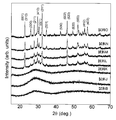
- FIG. 3 is a diagram showing X-ray diffraction patterns of Sample A of Example 1 and Samples D to I obtained by heat-treating Sample A.
- FIG. 6 is a diagram showing X-ray diffraction patterns of Sample B of Example 2 and Samples J to O obtained by heat-treating Sample B.
- FIG. 6 is a diagram showing an X-ray diffraction pattern of sample C of Example 3 and samples P to U obtained by heat-treating sample C.
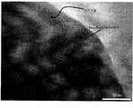
- 3 is a transmission electron micrograph of sample N powder obtained in Example 2.
- FIG. In Example 4 it is a schematic diagram which shows the system which measures the light modulation characteristic of the produced light modulation material.
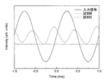
- Example 4 it is a figure which shows the result of the light modulation measurement of the sample B and the sample M.
- the “mother glass” means a glass that crystallizes by heat treatment and precipitates a target crystal. When this mother glass is heat-treated, glass ceramics in which tungsten bronze type Sr x Ba 1-x Nb 2 O 6 (0.25 ⁇ x ⁇ 0.75) crystals are present uniformly over the entire glass can be obtained.
- the method for producing the mother glass is not particularly limited as long as it is a practical method for producing a glass material.
- a melt quench method in which a glass body is obtained by rapidly cooling a glass melt is particularly preferable.
- the raw material include inorganic salts containing strontium, barium, niobium, and boric acid (particularly, oxides and carbonates are preferred), organometallic compounds, and composite oxides such as SBN crystal powder.
- the type of the reagent is not particularly limited as long as the reagent can be adjusted to have a desired composition.
- Patent Document 1 discloses the production of crystallized glass by adding a nucleating agent material, it can be easily assumed that crystallization can be promoted by adding a generally known nucleating agent.
- ions known as nucleating agents dissolve in the crystal, and as a result, the electrical characteristics inherent in the crystal may not be exhibited.
- oxides other than the oxide (SrO, BaO, Nb 2 O 5 ) constituting the target crystal it is not preferable to add oxides other than the oxide (SrO, BaO, Nb 2 O 5 ) constituting the target crystal to the crystallized glass except for the glass constituting oxide (B 2 O 3 ).
- the melting of the glass raw material is not particularly limited as long as the temperature is equal to or higher than the liquid phase of the SBN crystal. Considering homogenization of the melt and volatilization of boric acid, a suitable melting temperature is approximately 1000 to 1450 ° C. When the melting temperature is higher than 1450 ° C., boric acid is volatilized and it is difficult to obtain a homogeneous glass.
- a composition in which an SBN crystal exhibiting high transparency and sufficiently exhibiting an electrooptic effect is precipitated is preferable.
- aSrO-bBaO-cNb 2 O 5 -dB 2 O 3 and a + b + c + d 100
- a composition of 60 ⁇ (a + b + c) ⁇ 80, 20 ⁇ d ⁇ 40 is preferable
- the numerical values of a, b, c, and d correspond to mol% display of the glass composition.
- a composition of 25 ⁇ d ⁇ 38 is preferable. If d is less than 25, vitrification becomes difficult. On the other hand, if d is larger than 38, vitrification is easy, but the volume fraction of the SBN crystal is small, and the action length of the optical modulator may be long.
- the crystal grain size (average particle size) is preferably about 0.05 to 100 nm, and particularly preferably about 0.1 to 60 nm.
- the volume fraction of crystal grains in the sample after the heat treatment is preferably 20 to 75%, particularly preferably 25 to 70%. When the volume fraction is less than 20%, the amount of change in the refractive index due to the electro-optic effect becomes remarkably small, so that the action length of the optical modulator may be increased. On the other hand, if the volume fraction exceeds 75%, the difference in refractive index from the remaining glass becomes large, which may increase light scattering.
- the heat treatment temperature is preferably in the region from the glass transition temperature of the mother glass from ⁇ 80 ° C. to the crystallization start temperature. Particularly preferred is a temperature range from the crystallization start temperature of ⁇ 60 ° C. to the crystallization start temperature. Heat treatment is preferably performed at a constant temperature in this temperature range.
- the heat treatment time is not particularly limited, but approximately 10 to 72 hours are required to obtain a sufficient volume fraction.
- electrodes 2 and 2 are formed on both side surfaces of a region (optical waveguide) in which light of light modulating material 1 made of crystallized glass travels. Then, by applying a voltage having a desired modulation signal to this optical modulator, the optical modulator can be optically modulated.
- a conductive metal thin film of gold, platinum, silver, copper, nickel, chromium, or the like it is preferable to form a conductive metal thin film of gold, platinum, silver, copper, nickel, chromium, or the like by sputtering, coating, vacuum deposition, or the like.
- phase modulator By entering linearly polarized light into the optical modulator through the polarizer 4 and providing an analyzer 7 orthogonal to the polarization direction at the output end, a phase modulator can be manufactured. Modulation can be detected by changing the phase difference of incident light caused by the application of an electric field.
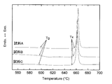
- FIG. 1 shows the DTA pattern of the bulk material of glass A produced.
- the glass transition temperature Tg was 599 ° C.
- the crystallization start temperature Tx was 669 ° C.
- Example 1 Production of crystallized glass
- the glass A produced in Production Example 1 was polished.
- the glass A was subjected to a crystallization treatment by performing a heat treatment for 10 hours at a temperature shown in Table 2 from the vicinity of the glass transition temperature to the crystallization temperature.
- the thermophysical properties of the obtained samples D to I are shown in Table 2, and the X-ray diffraction pattern is shown in FIG.
- the numbers in parentheses in the figure indicate the Miller index of Sr 0.5 Ba 0.5 Nb 2 O 6 crystal.
- the diffraction peak positions confirmed in the samples F to I were the same as those of the known Sr 0.5 Ba 0.5 Nb 2 O 6 crystal (ICSD # 240388).
- Example 2 In Example 1, the glass B obtained in Production Example 2 was used in place of the glass A.
- the glass B was subjected to crystallization treatment by performing a heat treatment for 10 hours at a temperature shown in Table 3 from the vicinity of the glass transition temperature to the crystallization temperature.
- the thermophysical properties of the obtained samples J to O are shown in Table 3, and the X-ray diffraction pattern is shown in FIG.
- the numbers in parentheses in the figure indicate the Miller index of Sr 0.61 Ba 0.39 Nb 2 O 6 crystal.
- the diffraction peak positions confirmed in the samples L to O were the same as those of the known Sr 0.61 Ba 0.39 Nb 2 O 6 crystal (ICSD # 240389).
- Example 3 In Example 1, the glass C obtained in Production Example 3 was used in place of the glass A. Glass C was subjected to a crystallization treatment by performing a heat treatment for 10 hours at a temperature shown in Table 4 from the vicinity of the glass transition temperature to the crystallization temperature. The thermophysical properties of the obtained samples P to U are shown in Table 4, and the X-ray diffraction pattern is shown in FIG. The numbers in parentheses in the figure indicate the Miller index of Sr 0.75 Ba 0.25 Nb 2 O 6 crystal.
- the diffraction peak positions of the RU samples were partially confirmed by diffraction derived from SrNb 2 O 6 (marked with ⁇ in the figure), but otherwise known Sr 0.75 Ba 0.25 Nb 2 O 6 crystals (ICSD # 15614) was the same.
- Sr 0.75 Ba 0.25 Nb 2 O 6 crystals (ICSD # 15614) was the same.
- the lattice constant of the crystal was estimated using the Scherrer equation, it was found to have an average particle diameter of 20 to 40 nm.
- the crystallization was insufficient with the heat treatment for 10 hours, but the crystallization proceeded in the same manner as the RU samples by further extending the heat treatment time.
- the average particle diameter of the crystals in samples I, O, and U obtained by heat-treating each of the glasses A, B, and C at the respective crystallization start temperatures (Tx) exceeds 60 nm. It was found that the particle size increases with increasing heat treatment temperature.
- FIG. 5 is a transmission electron micrograph taken using “JEM-2010” manufactured by JEOL Ltd. for the sample N powder subjected to the crystallization treatment in Example 2. From FIG. 5, it can be seen that one particle is composed of an elliptical Sr 0.61 Ba 0.39 Nb 2 O 6 crystal single phase of about 34 nm in the longitudinal direction and about 16 nm in the minor axis direction. The other samples D to U were evaluated in the same manner, and it was confirmed that the average grain size of the crystals was about the same as that obtained using the Scherrer equation.
- Example 4 Formation of electrodes and measurement of light modulation characteristics
- Sample B used as a raw material in Example 2 and Sample M crystallized by heat treatment were cut into 1 mm ⁇ 1.5 mm ⁇ 10 mm. After all surfaces were mirror-polished, a silver paste was applied to both sides of 1.5 mm ⁇ 10 mm and dried to form thin film electrodes.
- FIG. 6 is a schematic diagram showing a system for measuring the light modulation characteristics of the produced light modulation material. In this system, the electrodes 2 and 2 of the sample (light modulation material) 1 obtained above were connected to a high-voltage AC power source 3.
- a linearly polarized semiconductor laser 5 (wavelength 650 nm) that passes through the polarizer 4 is introduced from one of the 1 mm ⁇ 10 mm surfaces of the sample 1 and enters a crossed Nicols state through the quarter-wave plate 6 and the analyzer 7. Arranged. The direction of application of the electric field and the direction of vibration of the electric field vector of linearly polarized light are inclined by 45 °. The amount of light transmitted through the analyzer 6 was detected by a Si photodiode 8, amplified by a signal amplifier 9, and a change in output light intensity due to application of an electric field was measured with an oscilloscope 10.
- FIG. 7 shows the results of light modulation measurement of samples B and M. This figure shows a change in output light intensity when a ⁇ 3 kV sine wave is applied at 1 kHz with respect to a distance between electrodes of 1 mm.
- sample B that had not been crystallized, no change in strength appeared.
- the crystallized sample M showed a 2 kHz waveform that was twice 1 kHz, indicating that phase modulation due to the electro-optic effect occurred.
- the light modulation measurement was performed on each sample obtained in Examples 1 to 3
- a clear change in retardation was similarly shown.
- the effective value of the electro-optic coefficient was about 1.5 pm / V.
- glass ceramics in which tungsten bronze SBN crystals having a crystal diameter of several tens of nanometers are uniformly dispersed in glass can be obtained.
- the scattering loss is reduced by making the crystal diameter of the SBN polycrystal smaller than the wavelength of light, and even when it becomes a nanocrystal, the electro-optic coefficient can be expressed as an effective value of several pm / V. It was.
- a conventional light modulation material using single crystal glass does not respond at all to light orthogonal to the polarization axis.
- the light modulation material of the present invention can eliminate the polarization dependence of the conventional light modulation material.
- the light modulation material obtained in the present invention is suitably used for optical components such as an optical modulator, an optical switching element, a waveguide, and an attenuator.
Landscapes
- Chemical & Material Sciences (AREA)
- Engineering & Computer Science (AREA)
- Physics & Mathematics (AREA)
- Dispersion Chemistry (AREA)
- Chemical Kinetics & Catalysis (AREA)
- Organic Chemistry (AREA)
- Ceramic Engineering (AREA)
- Crystallography & Structural Chemistry (AREA)
- Nonlinear Science (AREA)
- Life Sciences & Earth Sciences (AREA)
- Materials Engineering (AREA)
- General Chemical & Material Sciences (AREA)
- Geochemistry & Mineralogy (AREA)
- Optics & Photonics (AREA)
- General Physics & Mathematics (AREA)
- Glass Compositions (AREA)
- Optical Modulation, Optical Deflection, Nonlinear Optics, Optical Demodulation, Optical Logic Elements (AREA)
Abstract
La présente invention concerne un matériau de modulation optique transparent qui est créé à partir d'une vitrocéramique dans laquelle des cristaux de bronze de tungstène SrxBa1-xNb2O6 (où 0,25 ≤ x ≤ 0,75) sont uniformément présents dans un verre qui est créé à partir d'un oxyde répondant à la formule chimique aSrO-bBaO-cNb2O5-dB2O3 (où a + b + c + d = 100 et (a + b + c) > 60). Elle concerne également un procédé de fabrication du matériau de modulation optique transparent. Le matériau de modulation optique transparent est composé d'un matériau composite de cristaux de SrxBa1-xNb2O6 et d'un verre, et possède une transparence élevée et une fraction volumique élevée des cristaux de SrxBa1-xNb2O6.
Applications Claiming Priority (2)
| Application Number | Priority Date | Filing Date | Title |
|---|---|---|---|
| JP2009047374 | 2009-02-27 | ||
| JP2009-047374 | 2009-02-27 |
Publications (1)
| Publication Number | Publication Date |
|---|---|
| WO2010098227A1 true WO2010098227A1 (fr) | 2010-09-02 |
Family
ID=42665437
Family Applications (1)
| Application Number | Title | Priority Date | Filing Date |
|---|---|---|---|
| PCT/JP2010/052238 Ceased WO2010098227A1 (fr) | 2009-02-27 | 2010-02-16 | Matériau de modulation optique et son procédé de fabrication |
Country Status (2)
| Country | Link |
|---|---|
| JP (1) | JP5717349B2 (fr) |
| WO (1) | WO2010098227A1 (fr) |
Cited By (4)
| Publication number | Priority date | Publication date | Assignee | Title |
|---|---|---|---|---|
| CN107903072A (zh) * | 2017-11-01 | 2018-04-13 | 浙江大学 | 两步共沉淀法制备铌酸锶钡纳米粉体的方法 |
| CN111268904A (zh) * | 2020-03-09 | 2020-06-12 | 上海大学 | 节能玻璃的制备方法 |
| CN114685042A (zh) * | 2016-06-17 | 2022-07-01 | 康宁股份有限公司 | 屏蔽近红外的透明玻璃陶瓷 |
| US12552704B2 (en) | 2017-10-23 | 2026-02-17 | Corning Incorporated | Glass-ceramics and glasses |
Families Citing this family (1)
| Publication number | Priority date | Publication date | Assignee | Title |
|---|---|---|---|---|
| CN103636083B (zh) | 2011-07-11 | 2019-04-19 | 株式会社V技术 | 脉冲激光振荡器以及脉冲激光振荡控制方法 |
Citations (4)
| Publication number | Priority date | Publication date | Assignee | Title |
|---|---|---|---|---|
| JPH08211343A (ja) * | 1995-02-06 | 1996-08-20 | Sony Corp | 電気光学変調器 |
| JP2002519299A (ja) * | 1998-07-06 | 2002-07-02 | コーニング インコーポレイテッド | タンタル含有ガラスおよびガラスセラミック |
| JP2003335551A (ja) * | 2002-03-15 | 2003-11-25 | Ohara Inc | Sbn系結晶化ガラス |
| WO2005075378A1 (fr) * | 2004-02-06 | 2005-08-18 | Murata Manufacturing Co.,Ltd. | Composition de ceramique ferroelectrique et dispositif d’application en ferroelectricite utilisant ladite composition |
Family Cites Families (3)
| Publication number | Priority date | Publication date | Assignee | Title |
|---|---|---|---|---|
| JP2003270597A (ja) * | 2002-03-19 | 2003-09-25 | Kyocera Corp | 光可変減衰装置 |
| JP3828478B2 (ja) * | 2002-10-18 | 2006-10-04 | 日本電信電話株式会社 | 光学変調方法および装置 |
| JP5006748B2 (ja) * | 2007-10-10 | 2012-08-22 | 株式会社リコー | 電気光学素子及び光ビーム偏向器 |
-
2010
- 2010-02-16 WO PCT/JP2010/052238 patent/WO2010098227A1/fr not_active Ceased
- 2010-02-25 JP JP2010039468A patent/JP5717349B2/ja active Active
Patent Citations (4)
| Publication number | Priority date | Publication date | Assignee | Title |
|---|---|---|---|---|
| JPH08211343A (ja) * | 1995-02-06 | 1996-08-20 | Sony Corp | 電気光学変調器 |
| JP2002519299A (ja) * | 1998-07-06 | 2002-07-02 | コーニング インコーポレイテッド | タンタル含有ガラスおよびガラスセラミック |
| JP2003335551A (ja) * | 2002-03-15 | 2003-11-25 | Ohara Inc | Sbn系結晶化ガラス |
| WO2005075378A1 (fr) * | 2004-02-06 | 2005-08-18 | Murata Manufacturing Co.,Ltd. | Composition de ceramique ferroelectrique et dispositif d’application en ferroelectricite utilisant ladite composition |
Non-Patent Citations (1)
| Title |
|---|
| KORTAN, A.R. ET AL.: "Novel ferroelectric ceram-glass of [ (Sr0) y (Ba0) (1_y) (Nb205) ] tellurite", J. MATER. RES., vol. 17, no. 5, May 2002 (2002-05-01), pages 1208 - 1212 * |
Cited By (7)
| Publication number | Priority date | Publication date | Assignee | Title |
|---|---|---|---|---|
| CN114685042A (zh) * | 2016-06-17 | 2022-07-01 | 康宁股份有限公司 | 屏蔽近红外的透明玻璃陶瓷 |
| US12590026B2 (en) | 2016-06-17 | 2026-03-31 | Corning Incorporated | Manufacturing tungsten bronze glass ceramic |
| US12552704B2 (en) | 2017-10-23 | 2026-02-17 | Corning Incorporated | Glass-ceramics and glasses |
| CN107903072A (zh) * | 2017-11-01 | 2018-04-13 | 浙江大学 | 两步共沉淀法制备铌酸锶钡纳米粉体的方法 |
| CN107903072B (zh) * | 2017-11-01 | 2020-04-28 | 浙江大学 | 两步共沉淀法制备铌酸锶钡纳米粉体的方法 |
| CN111268904A (zh) * | 2020-03-09 | 2020-06-12 | 上海大学 | 节能玻璃的制备方法 |
| CN111268904B (zh) * | 2020-03-09 | 2022-07-12 | 上海大学 | 节能玻璃的制备方法 |
Also Published As
| Publication number | Publication date |
|---|---|
| JP5717349B2 (ja) | 2015-05-13 |
| JP2010222240A (ja) | 2010-10-07 |
Similar Documents
| Publication | Publication Date | Title |
|---|---|---|
| TWI235139B (en) | Tantalum containing glasses and glass ceramics | |
| US7591961B2 (en) | Translucent piezoelectric glass ceramic | |
| TW567174B (en) | Transparent gallate glass-ceramics | |
| JP5717349B2 (ja) | 光変調材料およびその製造方法 | |
| CN105220232A (zh) | 具有梯度折射率效应的二次电光晶体及其制备与应用方法 | |
| JP2006512274A (ja) | ZnOベースのガラスセラミック | |
| JP4166032B2 (ja) | Sbn系結晶化ガラス | |
| JP3511204B2 (ja) | 光機能素子、該素子用単結晶基板、およびその使用方法 | |
| CN103882524A (zh) | 一种离子掺杂型电光晶体材料的制备与应用 | |
| Komatsu et al. | Fabrication of transparent tellurite glasses containing potassium niobate crystals by an incorporation method | |
| CN114481321B (zh) | 一种电光晶体硼铌酸钾及其应用 | |
| RU2429210C1 (ru) | Наноструктурированное поляризованное стекло и способ его получения | |
| Masai et al. | Preparation of crystallized glass for application in fiber-type devices | |
| CN117401906B (zh) | 一种铁电微纳米晶玻璃、制备及应用 | |
| Guerra et al. | Investigation of the physical properties of new PZT modified tellurium oxide (TeO2–B2O3–PbO2: TBP) glasses | |
| CN117305982B (zh) | 一种新型硅酸镓镧族晶体及其电光系数优化方法和应用 | |
| CN118954949B (zh) | 一种具有优异声光性能的碲酸盐玻璃、制备方法及其在声光调制器中的应用 | |
| Intawin et al. | Preparation and Characterization of SrFe12O19 on Optical and Dielectric Properties of Na2O-CaO-P2O5 Glasses | |
| Yongsiri et al. | Dielectric properties and microstructural studies of Er2O3 doped potassium sodium niobate silicate glass-ceramics | |
| JPH0412095A (ja) | ニオブ酸リチウム単結晶薄膜の製造方法 | |
| Chatterjee et al. | Studies of Crystallization Kinetics of Eu-doped Sodium Niobate Glass–Ceramics and Characterization of Its Microstructure, Thermal and Optical Properties | |
| CN121629515A (zh) | 硼铌酸钾电光晶体及其制备方法和用途 | |
| CN118996626A (zh) | 硼酸铷钡钪双折射晶体及其制备方法和应用 | |
| Kosaka et al. | Crystallization of langasite-type phases in gallium germanate glasses and optical properties of crystallized glasses | |
| JP3909845B2 (ja) | 光機能素子の製造方法 |
Legal Events
| Date | Code | Title | Description |
|---|---|---|---|
| 121 | Ep: the epo has been informed by wipo that ep was designated in this application |
Ref document number: 10746108 Country of ref document: EP Kind code of ref document: A1 |
|
| NENP | Non-entry into the national phase |
Ref country code: DE |
|
| 122 | Ep: pct application non-entry in european phase |
Ref document number: 10746108 Country of ref document: EP Kind code of ref document: A1 |