WO2010100971A1 - Matériau de base comportant un film mince - Google Patents
Matériau de base comportant un film mince Download PDFInfo
- Publication number
- WO2010100971A1 WO2010100971A1 PCT/JP2010/050768 JP2010050768W WO2010100971A1 WO 2010100971 A1 WO2010100971 A1 WO 2010100971A1 JP 2010050768 W JP2010050768 W JP 2010050768W WO 2010100971 A1 WO2010100971 A1 WO 2010100971A1
- Authority
- WO
- WIPO (PCT)
- Prior art keywords
- film
- density
- discharge
- electrode
- layer
- Prior art date
- Legal status (The legal status is an assumption and is not a legal conclusion. Google has not performed a legal analysis and makes no representation as to the accuracy of the status listed.)
- Ceased
Links
Images


Classifications
-
- C—CHEMISTRY; METALLURGY
- C23—COATING METALLIC MATERIAL; COATING MATERIAL WITH METALLIC MATERIAL; CHEMICAL SURFACE TREATMENT; DIFFUSION TREATMENT OF METALLIC MATERIAL; COATING BY VACUUM EVAPORATION, BY SPUTTERING, BY ION IMPLANTATION OR BY CHEMICAL VAPOUR DEPOSITION, IN GENERAL; INHIBITING CORROSION OF METALLIC MATERIAL OR INCRUSTATION IN GENERAL
- C23C—COATING METALLIC MATERIAL; COATING MATERIAL WITH METALLIC MATERIAL; SURFACE TREATMENT OF METALLIC MATERIAL BY DIFFUSION INTO THE SURFACE, BY CHEMICAL CONVERSION OR SUBSTITUTION; COATING BY VACUUM EVAPORATION, BY SPUTTERING, BY ION IMPLANTATION OR BY CHEMICAL VAPOUR DEPOSITION, IN GENERAL
- C23C16/00—Chemical coating by decomposition of gaseous compounds, without leaving reaction products of surface material in the coating, i.e. chemical vapour deposition [CVD] processes
- C23C16/44—Chemical coating by decomposition of gaseous compounds, without leaving reaction products of surface material in the coating, i.e. chemical vapour deposition [CVD] processes characterised by the method of coating
- C23C16/54—Apparatus specially adapted for continuous coating
- C23C16/545—Apparatus specially adapted for continuous coating for coating elongated substrates
-
- B—PERFORMING OPERATIONS; TRANSPORTING
- B32—LAYERED PRODUCTS
- B32B—LAYERED PRODUCTS, i.e. PRODUCTS BUILT-UP OF STRATA OF FLAT OR NON-FLAT, e.g. CELLULAR OR HONEYCOMB, FORM
- B32B27/00—Layered products comprising a layer of synthetic resin
- B32B27/06—Layered products comprising a layer of synthetic resin as the main or only constituent of a layer, which is next to another layer of the same or of a different material
- B32B27/08—Layered products comprising a layer of synthetic resin as the main or only constituent of a layer, which is next to another layer of the same or of a different material of synthetic resin
-
- B—PERFORMING OPERATIONS; TRANSPORTING
- B32—LAYERED PRODUCTS
- B32B—LAYERED PRODUCTS, i.e. PRODUCTS BUILT-UP OF STRATA OF FLAT OR NON-FLAT, e.g. CELLULAR OR HONEYCOMB, FORM
- B32B5/00—Layered products characterised by the non- homogeneity or physical structure, i.e. comprising a fibrous, filamentary, particulate or foam layer; Layered products characterised by having a layer differing constitutionally or physically in different parts
- B32B5/14—Layered products characterised by the non- homogeneity or physical structure, i.e. comprising a fibrous, filamentary, particulate or foam layer; Layered products characterised by having a layer differing constitutionally or physically in different parts characterised by a layer differing constitutionally or physically in different parts, e.g. denser near its faces
- B32B5/145—Variation across the thickness of the layer
-
- C—CHEMISTRY; METALLURGY
- C23—COATING METALLIC MATERIAL; COATING MATERIAL WITH METALLIC MATERIAL; CHEMICAL SURFACE TREATMENT; DIFFUSION TREATMENT OF METALLIC MATERIAL; COATING BY VACUUM EVAPORATION, BY SPUTTERING, BY ION IMPLANTATION OR BY CHEMICAL VAPOUR DEPOSITION, IN GENERAL; INHIBITING CORROSION OF METALLIC MATERIAL OR INCRUSTATION IN GENERAL
- C23C—COATING METALLIC MATERIAL; COATING MATERIAL WITH METALLIC MATERIAL; SURFACE TREATMENT OF METALLIC MATERIAL BY DIFFUSION INTO THE SURFACE, BY CHEMICAL CONVERSION OR SUBSTITUTION; COATING BY VACUUM EVAPORATION, BY SPUTTERING, BY ION IMPLANTATION OR BY CHEMICAL VAPOUR DEPOSITION, IN GENERAL
- C23C16/00—Chemical coating by decomposition of gaseous compounds, without leaving reaction products of surface material in the coating, i.e. chemical vapour deposition [CVD] processes
- C23C16/44—Chemical coating by decomposition of gaseous compounds, without leaving reaction products of surface material in the coating, i.e. chemical vapour deposition [CVD] processes characterised by the method of coating
- C23C16/50—Chemical coating by decomposition of gaseous compounds, without leaving reaction products of surface material in the coating, i.e. chemical vapour deposition [CVD] processes characterised by the method of coating using electric discharges
- C23C16/505—Chemical coating by decomposition of gaseous compounds, without leaving reaction products of surface material in the coating, i.e. chemical vapour deposition [CVD] processes characterised by the method of coating using electric discharges using radio frequency discharges
-
- B—PERFORMING OPERATIONS; TRANSPORTING
- B32—LAYERED PRODUCTS
- B32B—LAYERED PRODUCTS, i.e. PRODUCTS BUILT-UP OF STRATA OF FLAT OR NON-FLAT, e.g. CELLULAR OR HONEYCOMB, FORM
- B32B2307/00—Properties of the layers or laminate
- B32B2307/20—Properties of the layers or laminate having particular electrical or magnetic properties, e.g. piezoelectric
- B32B2307/202—Conductive
-
- B—PERFORMING OPERATIONS; TRANSPORTING
- B32—LAYERED PRODUCTS
- B32B—LAYERED PRODUCTS, i.e. PRODUCTS BUILT-UP OF STRATA OF FLAT OR NON-FLAT, e.g. CELLULAR OR HONEYCOMB, FORM
- B32B2307/00—Properties of the layers or laminate
- B32B2307/20—Properties of the layers or laminate having particular electrical or magnetic properties, e.g. piezoelectric
- B32B2307/206—Insulating
-
- B—PERFORMING OPERATIONS; TRANSPORTING
- B32—LAYERED PRODUCTS
- B32B—LAYERED PRODUCTS, i.e. PRODUCTS BUILT-UP OF STRATA OF FLAT OR NON-FLAT, e.g. CELLULAR OR HONEYCOMB, FORM
- B32B2307/00—Properties of the layers or laminate
- B32B2307/20—Properties of the layers or laminate having particular electrical or magnetic properties, e.g. piezoelectric
- B32B2307/21—Anti-static
-
- B—PERFORMING OPERATIONS; TRANSPORTING
- B32—LAYERED PRODUCTS
- B32B—LAYERED PRODUCTS, i.e. PRODUCTS BUILT-UP OF STRATA OF FLAT OR NON-FLAT, e.g. CELLULAR OR HONEYCOMB, FORM
- B32B2307/00—Properties of the layers or laminate
- B32B2307/40—Properties of the layers or laminate having particular optical properties
-
- B—PERFORMING OPERATIONS; TRANSPORTING
- B32—LAYERED PRODUCTS
- B32B—LAYERED PRODUCTS, i.e. PRODUCTS BUILT-UP OF STRATA OF FLAT OR NON-FLAT, e.g. CELLULAR OR HONEYCOMB, FORM
- B32B2307/00—Properties of the layers or laminate
- B32B2307/50—Properties of the layers or laminate having particular mechanical properties
-
- B—PERFORMING OPERATIONS; TRANSPORTING
- B32—LAYERED PRODUCTS
- B32B—LAYERED PRODUCTS, i.e. PRODUCTS BUILT-UP OF STRATA OF FLAT OR NON-FLAT, e.g. CELLULAR OR HONEYCOMB, FORM
- B32B2307/00—Properties of the layers or laminate
- B32B2307/50—Properties of the layers or laminate having particular mechanical properties
- B32B2307/536—Hardness
-
- B—PERFORMING OPERATIONS; TRANSPORTING
- B32—LAYERED PRODUCTS
- B32B—LAYERED PRODUCTS, i.e. PRODUCTS BUILT-UP OF STRATA OF FLAT OR NON-FLAT, e.g. CELLULAR OR HONEYCOMB, FORM
- B32B2307/00—Properties of the layers or laminate
- B32B2307/50—Properties of the layers or laminate having particular mechanical properties
- B32B2307/546—Flexural strength; Flexion stiffness
-
- B—PERFORMING OPERATIONS; TRANSPORTING
- B32—LAYERED PRODUCTS
- B32B—LAYERED PRODUCTS, i.e. PRODUCTS BUILT-UP OF STRATA OF FLAT OR NON-FLAT, e.g. CELLULAR OR HONEYCOMB, FORM
- B32B2307/00—Properties of the layers or laminate
- B32B2307/70—Other properties
- B32B2307/72—Density
-
- B—PERFORMING OPERATIONS; TRANSPORTING
- B32—LAYERED PRODUCTS
- B32B—LAYERED PRODUCTS, i.e. PRODUCTS BUILT-UP OF STRATA OF FLAT OR NON-FLAT, e.g. CELLULAR OR HONEYCOMB, FORM
- B32B2457/00—Electrical equipment
-
- B—PERFORMING OPERATIONS; TRANSPORTING
- B32—LAYERED PRODUCTS
- B32B—LAYERED PRODUCTS, i.e. PRODUCTS BUILT-UP OF STRATA OF FLAT OR NON-FLAT, e.g. CELLULAR OR HONEYCOMB, FORM
- B32B2551/00—Optical elements
Definitions
- the present invention relates to a substrate having a thin film having a gradient structure with a continuous film density.
- Thin film products such as anti-reflective coatings require high film density and high film hardness to improve durability and abrasion resistance.
- a thin film with high film density and film hardness is directly formed on a soft film. Then, adhesion failure and crack generation become a problem.
- adhesion and cracking are improved by forming a laminate having a graded structure with respect to film density (for example, Patent Document 1).
- the interface between the medium density film and the medium density film and the high density film. The interface of the film does not necessarily have sufficient adhesion, and cracks are likely to occur.
- further performance improvement is required.
- the object of the present invention is to provide high film density, high film hardness, good adhesion to the substrate and between the constituent layers, and hardly cause cracks on a flexible substrate. High durability and high abrasion resistance It is to obtain a substrate having a thin film.
- the single-layer film having a configuration in which both sides of the high-film density region are sandwiched between regions where the film density continuously decreases in the thickness direction, or a unit composed of these laminated films,
- a thin film having a high film density and a high hardness with high abrasion resistance and durability in a thin film product can be obtained, and even when formed on a flexible substrate, a thin film that hardly causes poor adhesion or cracks. Is obtained.
- the present invention relates to a highly durable and highly wear-resistant thin film using a thin film such as a metal oxide, nitride, oxynitride or the like used for a thin film product such as an antireflection film and its production.
- a thin film such as a metal oxide, nitride, oxynitride or the like used for a thin film product such as an antireflection film and its production.
- a structure in which a low density film (low refractive index layer) of silicon oxide, a medium density film, and a high density film (high refractive index layer) such as titanium oxide are laminated on a soft resin film is well known.
- the present invention seeks to obtain a thin film having high durability and high abrasion resistance on a base material in which a plurality of layers having different densities are laminated as a thin film product.
- the present invention is a substrate on which a thin film of metal oxide, nitride, oxynitride or the like used for thin film products is formed, and the film density is continuously increased in the thickness direction on both sides of the high film density region.
- a single layer film having a structure sandwiched between regions where the decrease occurs, or a substrate having a laminated film and the ratio of the maximum value and the minimum value of the film density of the single layer film is 1.03 to It is a base material characterized by being 1.5.
- the substrate is characterized by using a single layer film having such a laminated film and having a gradient structure at such a film density.
- the so-called high film density region is usually a region exceeding 2.1 in the case of silicon oxide, for example, a high-density region close to the density of the bulk material in a thin film, and is a material such as alumina. If this is a region exceeding 3.5, for example, if it is titanium oxide, it is a region exceeding 4.0, and each region is formed with a film density close to the density of a dense bulk material.
- the high film density region is a relative meaning of a high film density region and a low film density region in a single layer, and in an absolute sense, a high-density film of the material. It does not mean that.
- the film density in the high film density region of the formed single layer film is absolutely close to that of the bulk material and the average film density is increased in an absolute sense, a so-called “high density” film is obtained.
- the film density of the region is formed at a relatively low film density and the average film density is set at a relatively low density, a so-called “low density” film is obtained.
- the film density is characterized by an inclination.
- the density of the low density region is the same, when this ratio is large (for example, 1.5), a “high density” film as a whole with an inclined structure is used, and when the ratio is close to the minimum (for example, 1.03), “low density” Constitutes the membrane.
- the ratio between the maximum value and the minimum value of the film density is in the range of 1.03 to 1.5.
- a single layer film having a film density ratio within the range of the present invention has good adhesion to the substrate (also between the single layer films), film hardness, cracks, and the like. If the film density ratio is too small, as a result, in the case of a film having a high average film density, the adhesiveness is lowered and cracks and the like are easily generated. When the average film density is low, there is a problem with the film hardness. On the other hand, if the film density ratio is too large, the adhesion is good, but the cracks deteriorate and the film hardness of the surface also decreases.
- such a thin film having a continuously inclined structure in the film thickness direction is, for example, a coating method, a vapor deposition method, a sputtering method, a spray pyrolysis method, a low pressure plasma CVD method, an atmospheric pressure plasma CVD method.
- the method is not limited, but a method suitable for a continuous process is preferable in order to obtain a high productivity using a flexible substrate. Among them, atmospheric pressure plasma is preferable from the viewpoint of continuous productivity and film quality.
- the CVD method is preferred.
- a dense high film density thin film is formed in a plasma space where the discharge intensity is high, and a low film density film is formed where the discharge intensity is low. Accordingly, a film having a high film density is formed when the discharge output is large, and a film having a low film density is formed when the discharge output is small.
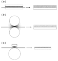
- FIG. 1A shows an electrode arrangement of a plasma CVD processing apparatus having parallel plate electrodes. Since the gap between the electrodes between the parallel electrodes is uniform, the discharge intensity is also substantially uniform, and between the parallel plate electrodes. A monolayer film having a substantially uniform film density can be formed on a substrate conveyed (or placed) in the discharge space. When the discharge output is increased, the discharge intensity is increased and a film having a high film density is formed. When the discharge output is decreased, a film having a low film density is formed.
- the discharge intensity is approximately proportional to the emission intensity in the discharge space, the emission intensity and the film density are substantially correlated.
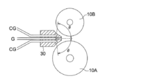
- FIG. 1B shows an outline of the electrode arrangement of the counter roll type plasma CVD processing apparatus.
- the discharge output is increased between the counter roll electrodes, the discharge spreads in the roll circumferential direction.
- the discharge intensity is distributed in the discharge space between the roll electrodes. That is, the discharge intensity is high in the central part where the discharge gap (interelectrode gap) is narrow, and the discharge intensity is low where the discharge gap is wide, away from the roll circumferential direction.
- FIG. 1A When the parallel plate electrode is used in FIG. 1 (a), and when the counter roll type plasma CVD discharge treatment apparatus is used in FIG. 1 (b), the discharge intensity distribution between the respective electrodes and the substrate
- FIG. 1B a single-layer film having a uniform film density profile is shown.
- FIG. 1B both sides of the maximum film density region are regions where the film density continuously decreases in the thickness direction.
- a single-layer film having an inclined structure in which the film density is sandwiched is obtained.
- the substrate transported between the opposed roll electrodes is first formed into a film in a discharge space that is circumferentially separated from the center of the electrode where the discharge gap is the narrowest. While being transported, the film is gradually deposited at the portion of the discharge center where the discharge gap is the narrowest and the discharge intensity is large, and after this, the film is deposited again in the discharge space away from the center in the roll circumferential direction. Therefore, when looking at the film thickness profile, a single layer film having a gradient structure in which the film density sandwiched between the areas where the film density continuously decreases in the thickness direction on both sides of the maximum film density area can be obtained.
- the film thickness of such a single layer film having an inclined structure with a film density formed using a counter roll type plasma CVD discharge processing apparatus is determined by the transport speed, and the film thickness depends on the discharge conditions together with the transport speed.
- a density profile (maximum film density, minimum film density) is determined.
- the region having the maximum film density is defined as one of the discharge gaps after the substrate is left in the discharge space and the film is formed under the same discharge conditions in the plasma CVD apparatus.
- the film density of the film formed at the narrowest electrode center corresponds to the film density of the thin film formed in the discharge space separated in the circumferential direction of the roll electrode.
- the density of the thin film formed on the resin substrate can be determined using a known analysis means, but in the present invention, the value determined by the X-ray reflectance method is used.
- the X-ray reflectivity method is a method in which X-rays are incident on a material having a flat surface at a very shallow angle, and measurement is performed using MXP21 manufactured by Mac Science. Copper is used as the target of the X-ray source and it is operated at 42 kV and 500 mA. A multilayer parabolic mirror is used for the incident monochromator.
- the incident slit is 0.05 mm ⁇ 5 mm, and the light receiving slit is 0.03 mm ⁇ 20 mm.
- Measurement is performed by the FT method with a step width of 0.005 ° and a step of 10 seconds from 0 to 5 ° in the 2 ⁇ / ⁇ scan method. With respect to the obtained reflectance curve, Reflectivity Analysis Program Ver.
- Curve fitting is performed using 1, and each parameter is obtained so that the residual sum of squares of the actual measurement value and the fitting curve is minimized. From each parameter, the thickness and density of the laminated film can be obtained.
- the film thickness evaluation of the laminated film in the present invention can also be obtained from the X-ray reflectivity measurement.
- the density of a ceramic film such as silicon oxide, silicon nitride, or silicon oxynitride formed by another method such as an atmospheric pressure plasma method or a vapor deposition method can be measured.
- the present invention when a film is formed on a substrate, a low-density and therefore flexible film is formed at the initial stage of the film formation, so that the film is well attached and the substrate is also cracked by bending or the like. It becomes a difficult film.
- the interface is an interface between low-density films, Good adhesion and good film.
- the low density region is flexible and has a stress relieving effect, when such a single layer film is used, cracks and the like are generated even when a plurality of layers are stacked as compared with the case where a single layer is formed with a high density film. Hateful.
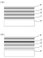
- FIG. 3A is a cross-sectional view schematically showing an example in which such single-layer films having the same average film density are stacked.
- FIG. 3B is a cross-sectional view showing an example in which a plurality of single-layer films having different average film densities and gradient structures are laminated.
- four single-layer films having different average film densities are laminated as one unit, and the average film density of each layer (unit) is, for example, base material F / layer 1 ⁇ layer 2 ⁇ layer 3> layer. 4 can be designed.
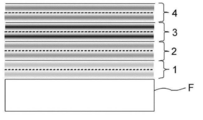
- FIG. 4 shows an example in which a single layer film having an inclined structure with the same average film density is laminated to form one unit, and this unit is laminated.
- a plurality of units having different average film densities are stacked using a unit in which a plurality of single-layer films having an inclined film density are stacked, and the average film density of each layer unit as described above is determined as layer unit 1 ⁇ It can also be designed as layer unit 2 ⁇ layer unit 3> layer unit 4.
- FIG. 4 schematically shows this example.
- two layers of single-layer films having a gradient structure in the film density are stacked to form one unit, but may be composed of three or more layers. Even if the number of single-layer films constituting one unit increases (even if the layer thickness increases), cracks and peeling occur as compared to a uniform single-layer film having the same film density and the same film thickness. A laminated film having flexibility that is difficult to crack and hardly cracks is formed.
- a film unit formed by laminating two single-layer films having an inclined film density structure is easily formed by using an atmospheric pressure plasma CVD processing apparatus having a counter roll electrode as shown in FIG. 7 described later. .
- the roll-shaped substrate is subjected to the plasma discharge treatment twice, the thin film having the continuous gradient structure as described above is laminated and formed twice. Therefore, when this is used as one unit and a plurality of thin films are further formed under different discharge conditions, the base material on which the units having different average film densities shown in FIG. 4 are stacked can be obtained.
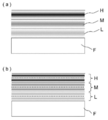
- FIG. 5 shows an antireflection film in which a uniform low-density layer (low refractive index) L, medium-density layer (medium refractive index) M, and high-density layer (high refractive index) H are laminated on a substrate F.
- L uniform low-density layer
- M medium-density layer
- H high-density layer
- the refractive index of the high-density layer is, for example, 1.8 to 2.2 as the refractive index for a light beam with a wavelength of 450 nm, and the refractive index of the low-density layer (low refractive index) is 1.4. This is configured to be about 1.6 or less, and the intermediate density layer is selected to have an intermediate refractive index.
- the stress relaxation action of the low density film is used to prevent a certain amount of bending, thermal expansion and the like from causing cracks.
- FIG. 6 shows an example in which these laminates are formed using the single layer film of the present invention having a gradient structure in film density.
- the single layer film of the present invention having different average film densities is used as a low density layer (low refractive index) L, a medium density layer (medium refractive index) M, and a high density layer (high refractive index) H.
- two single-layer films of the present invention having the same average film density are laminated to form a layer unit as a low-density layer (low refractive index) L and a medium-density layer (medium
- M refractive index
- H high-density layer
- Each single-layer film with a different path can be confirmed by tomography.
- each single layer film itself has a gradient structure with respect to the film density, and further, a laminated structure of films having different average densities as a whole has a further stress relaxation effect. Adhesion is improved, and there is a great effect in suppressing cracks.
- the present invention can be carried out by utilizing the discharge intensity distribution using the opposed roll type atmospheric pressure plasma CVD processing apparatus.
- the discharge output is increased by the opposed roll method, the discharge spreads in the circumferential direction, and the discharge space has a discharge intensity distribution due to its curvature.
- the discharge gap is narrow, the discharge intensity is large, and at a wide portion, that is, at the discharge end, the discharge intensity is small.
- the density has an inclined structure in the thickness direction.
- the light emission intensity at the narrowest part of the discharge gap / the light emission intensity at the end of the discharge 1.5 or more, and it can be considered that the light emission intensity distribution ⁇ the discharge intensity distribution.
- the film density at the end is 1.5 or more.
- the ratio of the maximum value and the minimum value of the film density of the formed single layer film is 1.03. Adjust to be ⁇ 1.5.
- Those having a film density ratio in the range of the present invention have good adhesion to the substrate (and between the single-layer films), and also have good film hardness, cracks, and the like.
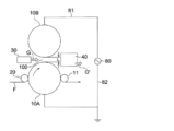
- FIG. 2 is an example of a plasma discharge treatment apparatus used in the present invention, and is a view schematically showing a plasma discharge treatment apparatus used for forming a thin film on a substrate using two roll electrodes.
- This plasma discharge processing apparatus has a pair of roll electrodes 10A and 10B having the same diameter, and a power supply 80 capable of applying a voltage for plasma discharge to these roll electrodes 10A and 10B is a voltage supply means 81. And 82 are connected.
- the roll electrodes 10 ⁇ / b> A and 10 ⁇ / b> B are rotating electrodes that can rotate while winding the base material F.
- the discharge unit (also referred to as discharge space) 100 is maintained at, for example, atmospheric pressure or a pressure in the vicinity thereof, the process gas G is supplied from the process gas supply unit 30, and plasma discharge is performed in the discharge unit 100 having the discharge space gap L. Is done.
- the base material F supplied from the pre-process or the former winding roll is brought into close contact with the roll electrode 10A by the guide roll 20 and rotated and transferred in synchronization, and is subjected to plasma discharge treatment by the processing gas G in the discharge section 100.
- the processing gas supply means 30 is preferably in the form of a slit that is the same as or slightly wider than the width of the base material, or pipe-shaped outlets are arranged side by side so as to be equivalent to the width of the base material.
- the processing gas G may be introduced into the discharge unit 100 at a uniform flow rate or flow rate throughout the width direction.
- the treated base material F passes through the roll 11 and is taken up or transferred to the next step (none is shown).
- the treated gas G ′ is exhausted from the exhaust port 40.
- the exhaust flow rate from the exhaust port 40 is preferably equal to or slightly higher than the flow rate from the processing gas supply means 30.
- the side surfaces of the roll electrodes 10A and 10B of the discharge unit 100 may be shielded, or the entire apparatus may be surrounded and filled with a rare gas or a processing gas.
- the processing gas supply means supplies a processing gas having an atmospheric pressure or a pressure near it between the counter electrodes, or a discharge space is formed under an atmospheric pressure or a pressure near it. It is preferable.
- Plasma discharge treatment equipment performed at or near atmospheric pressure does not need to be reduced in pressure compared to plasma CVD under vacuum, and is not only highly productive, but also has a high plasma density.
- the film-forming speed is high, and further, under high pressure conditions such as under atmospheric pressure compared with the conditions of normal CVD method, the mean free path of gas is very short, so that an extremely high quality film can be obtained.
- the vicinity of atmospheric pressure represents a pressure of 20 kPa to 110 kPa, but 93 kPa to 104 kPa is preferable for obtaining a good effect.
- FIG. 2 shows a plasma discharge processing apparatus having a power source 80 that can apply a voltage for a single plasma discharge to the roll electrodes, and a high-frequency power source in one frequency band.
- a power source having a different frequency is installed in each roll electrode. It is also a preferable aspect to use a plasma discharge treatment apparatus that superposes the first high-frequency electric field and the second high-frequency electric field to perform plasma discharge.
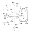
- FIG. 7 is a diagram schematically showing a plasma discharge processing apparatus for processing a substrate using a two-frequency roll electrode as another example of the plasma discharge processing apparatus used in the present invention.
- This apparatus has a pair of roll electrodes 10A (first electrode) and a roll electrode 10B (second electrode).
- a first power supply 801 capable of applying a high-frequency voltage V1 having a frequency ⁇ 1 for plasma discharge is connected to the roll electrode 10A via a voltage supply unit 811.
- a second power source 802 capable of applying a high-frequency voltage V2 having a frequency ⁇ 2 for plasma discharge is connected to the roll electrode 10B via a voltage supply unit 812.
- the first power source 801 preferably has the ability to apply a higher frequency voltage (V1> V2) than the second power source 802, and the first frequency ⁇ 1 of the first power source 801 and the second frequency of the second power source 802 are the same.
- the frequency ⁇ 2 is preferably ⁇ 1 ⁇ 2.
- a first filter is installed (omitted) so that a current from the first power source 801 flows toward the roll electrode 10A, and the first power source 801 is omitted.
- the current I1 from the second power source 802 is designed to be less likely to pass to the ground side, and the current I2 from the second power source 802 is easily passed to the ground side.
- a second filter is provided between the roll electrode 10B and the second power source 802 so that the current from the second power source 802 flows toward the roll electrode 10C (omitted).
- Current I2 is less likely to pass to the ground side, and current I1 from the first power source 801 is designed to easily pass to the ground side.
- V1 ⁇ IV> V2 or V1> IV ⁇ V2 is satisfied, and more preferably, V1> IV> V2.
- the frequency of the first power source is preferably 200 kHz or less.
- the electric field waveform may be a sine wave or a pulse.
- the lower limit is preferably about 1 kHz.
- the frequency of the second power source is preferably 800 kHz or more.
- the upper limit is preferably about 200 MHz.
- the base material F supplied from the pre-process or the former winding roll is brought into close contact with the roll electrode 10A by the guide roll 20 and rotated and transferred in synchronization, and is subjected to plasma discharge treatment by the processing gas G in the discharge section 100.
- the processing gas supply means 30 is preferably in the form of a slit that is the same as or slightly wider than the width of the base material, or pipe-shaped outlets are arranged side by side so as to be equivalent to the width of the base material.
- the processing gas G may be introduced into the discharge unit 100 at a uniform flow rate or flow rate throughout the width direction.
- the treated base material F passes through the folding rolls 11A, 11B, 11C and 11D, is transferred in the reverse direction, is held by the roll electrode 10B, is again subjected to plasma discharge treatment in the discharge unit 100, and is wound up through the guide roll 21. Or transferred to the next step (both not shown).
- the treated gas G ′ is exhausted from the exhaust port 40.
- the exhaust flow rate from the exhaust port 40 is preferably equal to or slightly higher than the flow rate from the processing gas supply means 30.
- the side surfaces of the roll electrodes 10A and 10B of the discharge unit 100 may be shielded, or the entire apparatus may be surrounded and filled with a rare gas or a processing gas.
- the processing gas supply means supplies a processing gas having an atmospheric pressure or a pressure near it between the counter electrodes, or a discharge space is formed under an atmospheric pressure or a pressure near it. It is preferable.
- FIG. 7 shows a configuration in which a two-frequency system is applied as an applied power source, and since the base material F is discharged twice under the same conditions, a single layer film having the same inclined structure in the film thickness direction. Two layers can be formed at a time, and the two-layered film unit shown in FIG. 4 can be formed at a time.
- first power source 2 high frequency power source
- Applied power symbol Manufacturer Frequency Product name A1 Shinko Electric 3kHz SPG3-4500 A2 Shinko Electric Co., Ltd. 5kHz SPG5-4500 A3 Kasuga Electric 15kHz AGI-023 A4 Shinko Electric 50kHz SPG50-4500 A5 HEIDEN Laboratory 100kHz * PHF-6k A6 Pearl Industry 200kHz CF-2000-200k And the like, and any of them can be used.
- Applied power supply symbol Manufacturer Frequency Product name B1 Pearl Industry 800 kHz CF-2000-800k B2 Pearl Industry 2MHz CF-2000-2M B3 Pearl Industry 13.56MHz CF-5000-13M B4 Pearl Industry 27MHz CF-2000-27M B5 Pearl Industry 150MHz CF-2000-150M B6 Pearl Industry 20-99.9MHz RP-2000-20 / 100M And the like, and any of them can be used.
- * indicates a HEIDEN Laboratory impulse high-frequency power source (100 kHz in continuous mode). Other than that, it is a high-frequency power source that can apply only a continuous sine wave.
- FIG. 8 is a schematic diagram showing an example of a gas supply unit applicable to the plasma discharge treatment apparatus.
- the processing gas G is blown out in the direction of the gap between the roll electrodes 10A and 10B.
- the gap between the roll electrodes is narrow at that time, the entire amount of the blown processing gas cannot necessarily pass through the gap. A part of the gas leaks from the gap between the processing gas supply means 30 and the roll electrode and blows out to the outside, so that an extra processing gas is required and the processing chamber is filled.
- the processing gas supply means 30 is provided with a blowout port that blows the auxiliary gas CG in the same direction as the process gas blowing direction as means for blocking the leaked processing gas.
- the processing gas G is composed of a discharge gas and a thin film forming gas
- the discharge gas is an inert gas such as a rare gas or nitrogen. It consists of reactive gas that promotes.
- the auxiliary gas CG is made of an inert gas such as a rare gas or nitrogen, and preferably has the same composition as the discharge gas in the processing gas G or the same composition as the discharge gas and the reactive gas.
- the flow rate at which the auxiliary gas is blown out is preferably equal to or higher than the flow rate at which the processing gas G is blown at the supply port of the processing gas supply means 30 to 5 times or less. If it is less than this, the effect of the auxiliary gas is small, and if it is 5 times or more, it becomes difficult to supply the processing gas G to the discharge space 100.
- the angle ⁇ at which the auxiliary gas CG is blown to the roll electrodes 10A and 10B is set between 0 ⁇ ⁇ ⁇ 90 °, and along with the effect as the auxiliary gas CG, the accompanying air flows from the side surface of the processing gas supply means 30 and the roll electrode 10A, It can prevent mixing from between 10C. And preferably 0 ⁇ ⁇ ⁇ 60 °, more preferably 0 ⁇ ⁇ ⁇ 30 °. This is because when the angle is 90 ° or more, the component of the auxiliary gas CG toward the discharge space 100 decreases, and the effect cannot be obtained.
- ⁇ is an angle formed by the direction in which the processing gas blows out and the direction in which the auxiliary gas blows out.
- the material of the gas supply unit 30 for supplying the processing gas G and the auxiliary gas CG is preferably an insulating material such as ceramic such as alumina or resin, and particularly preferably a heat resistant resin such as PEEK (polyether ether ketone).
- the plasma discharge treatment apparatus that can be used in the present invention is further exemplified.
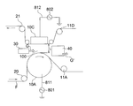
- FIG. 11 is a diagram schematically showing a plasma discharge processing apparatus for processing a substrate using a two-frequency roll electrode, which is an example of a plasma discharge processing apparatus in which only one side is a roll electrode and a counter electrode is a square rod electrode. It is.
- This apparatus has a roll electrode 10A (first electrode) and a square bar electrode 10C (second electrode).
- a first power supply 801 capable of applying a high-frequency voltage V1 having a frequency ⁇ 1 for plasma discharge is connected to the roll electrode 10A via a voltage supply unit 811.
- a second power source 802 capable of applying a high-frequency voltage V2 having a frequency ⁇ 2 for plasma discharge is connected to the rectangular rod-shaped electrode 10C via a voltage supply means 812.
- the first power source 801 preferably has the ability to apply a higher frequency voltage (V1> V2) than the second power source 802, and the first frequency ⁇ 1 of the first power source 801 and the second frequency of the second power source 802 are the same.
- the frequency ⁇ 2 is preferably ⁇ 1 ⁇ 2.
- a first filter is installed (omitted) so that a current from the first power source 801 flows toward the roll electrode 10A, and the first power source 801 is omitted.
- the current I1 from the second power source 802 is designed to be less likely to pass to the ground side, and the current I2 from the second power source 802 is easily passed to the ground side.
- a second filter is provided between the rectangular rod-shaped electrode 10C and the second power source 802 so that a current from the second power source 802 flows toward the roll electrode 10C (omitted), and the second power source 802 is omitted.
- the current I2 from the first power source 801 is designed to be easily passed to the ground side.
- V1 ⁇ IV> V2 or V1> IV ⁇ V2 is satisfied, and more preferably, V1> IV> V2.
- the frequency of the first power source is preferably 200 kHz or less.
- the electric field waveform may be a sine wave or a pulse.
- the lower limit is preferably about 1 kHz.
- the frequency of the second power source is preferably 800 kHz or more.
- the upper limit is preferably about 200 MHz.
- the base material F supplied from the pre-process or the former winding roll is brought into close contact with the roll electrode 10A by the guide roll 20 and rotated and transferred in synchronization, and is subjected to plasma discharge treatment by the processing gas G in the discharge section 100.
- the processing gas supply means 30 is preferably in the form of a slit that is the same as or slightly wider than the width of the base material, or pipe-shaped outlets are arranged side by side so as to be equivalent to the width of the base material.
- the processing gas G may be introduced into the discharge unit 100 at a uniform flow rate or flow rate throughout the width direction.
- the treated base material F is wound up through the guide roll 22 or transferred to the next step (none is shown).
- the base material F ′ transported in the reverse direction on the rectangular rod-shaped electrode 10C is a substrate for cleaning the rectangular rod-shaped electrode 10C, and a PET film or the like is used. 21 is wound up. Moreover, you may circulate and use.
- the treated gas G ′ is exhausted from the exhaust port 40.
- the exhaust flow rate from the exhaust port 40 is preferably equal to or slightly higher than the flow rate from the processing gas supply means 30.
- the side surfaces of the roll electrodes 10A and 10B of the discharge unit 100 may be shielded, or the entire apparatus may be surrounded and filled with a rare gas or a processing gas.
- the processing gas supply means supplies a processing gas having an atmospheric pressure or a pressure near it between the counter electrodes, or a discharge space is formed under an atmospheric pressure or a pressure near it. It is preferable.
- the same power supply (high frequency power supply) as that of the apparatus of FIG. 7 can be used as the first power supply (high frequency power supply) and the second power supply (high frequency power supply).
- the gas supply means is also shown in FIG.
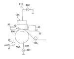
- FIG. 12 further shows another example of the plasma discharge treatment apparatus in which only one side is a roll electrode and the counter electrode is a square bar electrode.
- the one shown in FIG. 11 is a simpler plasma discharge treatment apparatus that does not use a cleaning base material for the square bar electrode 10C (second electrode), and is suitable for implementation on a small scale.
- the configuration of the apparatus shown in FIG. 11 is basically the same as that of the other parts, and the description thereof is omitted.
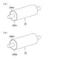
- FIG. 9 is a perspective view showing an example of an applicable roll electrode.
- the roll electrode 10 is inorganic after a ceramic is sprayed on a conductive base material 200a (hereinafter also referred to as “electrode base material”) such as metal. It is composed of a combination in which a ceramic-coated dielectric 200b (hereinafter also simply referred to as “dielectric”) coated with a material is covered.
- a ceramic-coated dielectric 200b hereinafter also simply referred to as “dielectric” coated with a material is covered.
- alumina, silicon nitride, or the like is preferably used. Among these, alumina is more preferably used because it is easily processed.
- the roll electrode 10 ′ may be constituted by a combination in which a conductive base material 200A such as metal is coated with a lining dielectric 200B provided with an inorganic material by lining.
- a conductive base material 200A such as metal
- a lining dielectric 200B provided with an inorganic material by lining.
- silicate glass, borate glass, phosphate glass, germanate glass, tellurite glass, aluminate glass, vanadate glass and the like are preferably used. Of these, borate glass is more preferred because it is easy to process.
- Examples of the conductive base materials 200a and 200A such as metal include metals such as silver, platinum, stainless steel, aluminum, and iron. Stainless steel is preferable from the viewpoint of processing.
- each roll electrode 10 it is desirable to adjust the temperature of each roll electrode 10 as necessary, such as heating or cooling.
- a liquid is supplied into the roll electrode to control the temperature of the electrode surface and the temperature of the substrate.
- an insulating material such as distilled water or oil is preferable.
- the temperature of the substrate varies depending on the treatment conditions, it is usually preferably room temperature to 200 ° C., more preferably room temperature to 120 ° C.
- the surface of the roll electrode is required to have high smoothness because the base material is in close contact and the base material and the electrode are transferred and rotated synchronously.
- the smoothness is expressed as the maximum surface roughness height (Rmax) and centerline average surface roughness (Ra) specified in JIS B 0601.
- Rmax of the surface roughness of the roll electrode according to the present invention is preferably 10 ⁇ m or less, more preferably 8 ⁇ m or less, and particularly preferably 7 ⁇ m or less.
- Ra is preferably 0.5 ⁇ m or less, and more preferably 0.1 ⁇ m or less.
- the gap between the roll electrodes is determined in consideration of the thickness of the solid dielectric, the magnitude of the applied voltage, the purpose of using plasma, the shape of the electrode, and the like.
- the distance between the electrode surfaces is preferably 0.5 to 20 mm, more preferably 0.5 to 5 mm, and particularly preferably 1 mm ⁇ 0.5 mm from the viewpoint of uniformly generating plasma discharge.
- the gap between the roll electrodes refers to a distance at which the opposing electrode surfaces are closest to each other.
- the diameter of the roll electrode is preferably 10 to 1000 mm, more preferably 20 to 500 mm.
- the peripheral speed of the roll electrode is 1 to 100 m / mim, more preferably 5 to 50 m / mim.
- Processing gas A processing gas used when forming a thin film of metal oxide, nitride, oxynitride, or the like according to the present invention using a plasma discharge processing apparatus will be described.
- the processing gas it is particularly preferable to use a mixed gas mainly of a discharge gas and a thin film forming gas (also called a reactive gas).
- Examples of useful discharge gas (also referred to as rare gas) elements include nitrogen and Group 18 elements of the periodic table, specifically nitrogen, helium, neon, argon, krypton, xenon, radon, and the like. In the present invention, nitrogen, helium, and argon are preferable, and nitrogen is particularly preferable.
- the concentration of the rare gas in the processing gas is preferably 90% by volume or more in order to generate stable plasma. 90 to 99.99% by volume is particularly preferable.
- the rare gas is necessary for generating plasma discharge, and the reactive gas in the plasma discharge is ionized or radicalized to contribute to the surface treatment.
- a low refractive index layer useful for an antireflection layer or the like can be formed by using a silicon compound as a thin film forming gas.
- an organometallic compound containing a metal such as Ti, Zr, Sn, Si, or Zn, a metal oxide layer or a metal nitride layer can be formed.
- a useful medium refractive index layer and high refractive index layer can be formed, and a conductive layer and an antistatic layer can also be formed.
- preferred examples of the reactive gas substance useful in the present invention include metal compounds.
- Examples of reactive gas metal compounds that can be preferably used in the present invention include Al, As, Au, B, Bi, Ca, Cd, Cr, Co, Cu, Fe, Ga, Ge, Hg, In, Li, Mg, and Mn. , Mo, Na, Ni, Pb, Pt, Rh, Sb, Se, Si, Sn, V, W, Y, Zn, Zr, and other metal compounds or organometallic compounds can be mentioned, and Al, Ge, In, Sb, Si, Sn, Ti, W, Zn or Zr is preferably used as the organometallic compound.
- silicon compounds include silicon such as alkyl silanes such as dimethylsilane and tetramethylsilane, tetramethoxysilane, tetraethoxysilane, tetrapropoxysilane, dimethyldiethoxysilane, methyltrimethoxysilane, and ethyltriethoxysilane.
- organosilicon compounds such as alkoxides; silicon hydrogen compounds such as monosilane and disilane, halogenated silicon compounds such as dichlorosilane, trichlorosilane, and tetrachlorosilane, and other organosilanes, all of which can be preferably used.
- the present invention is not limited to these.
- the above organosilicon compounds are preferably silicon alkoxides, alkylsilanes, and organosilicon hydrogen compounds. They are not corrosive, do not generate harmful gases, and have little contamination in the process. Silicon alkoxide is preferred.
- the metal compound other than silicon as the reactive gas useful in the present invention is not particularly limited, and examples thereof include organometallic compounds, halogenated metal compounds, and metal hydrogen compounds.
- the organic component of the organometallic compound is preferably an alkyl group, an alkoxide group, or an amino group, and preferred examples include tetraethoxy titanium, tetraisopropoxy titanium, tetrabutoxy titanium, and tetradimethylamino titanium.
- the metal halide compound include titanium dichloride, titanium trichloride, and titanium tetrachloride.
- examples of the metal hydrogen compound include monotitanium and dititanium.
- a titanium-based organometallic compound can be preferably used.
- any of gas, liquid or solid may be used at normal temperature and pressure, but if it is liquid or solid, heating It may be used after being vaporized by means of a vaporizer such as reduced pressure or ultrasonic irradiation. In the present invention, it is preferable to use it by vaporizing or evaporating it into a gaseous state. If the boiling point of the liquid organometallic compound at room temperature and normal pressure is 200 ° C. or less, vaporization can be facilitated, which is suitable for the production of the thin film of the present invention.
- the organometallic compound is a metal alkoxide such as tetraethoxysilane or tetraisopropoxytitanium, it is easily dissolved in an organic solvent, so that it can be diluted with an organic solvent such as methanol, ethanol, n-hexane or the like. Good.
- An organic solvent may be used as a mixed solvent.
- the content in the processing gas is preferably 0.01 to 10% by volume, more preferably 0.1 to 5%. % By volume.
- the above metal compounds may be used by mixing several kinds of the same or different metal compounds.
- an organosilicon compound is suitable for forming a low refractive index layer having a small average film density while having a gradient structure of the film density
- Titanium-based organometallic compounds are suitable for forming a high refractive index layer having a large average film density, and any of them is preferably used.
- the density (refractive index) can be controlled by adjusting the mixing ratio by using a gas in which these are mixed, so that a medium refractive index layer can be obtained.
- Examples of the substrate according to the present invention include a cellulose ester film, a polyester film, a polycarbonate film, a polystyrene film, a polyolefin film, a polyvinyl alcohol film, a cellulose film, and other resin films.
- a cellulose ester film As cellulose diacetate film, cellulose acetate butyrate film, cellulose acetate propionate film, cellulose acetate phthalate film, cellulose triacetate, cellulose nitrate; as polyester film, polyethylene terephthalate film, polyethylene naphthalate film, polybutylene phthalate film 1,4-dimethylenecyclohexylene tele Tallate or copolyester film of these structural units; polycarbonate film of bisphenol A; polystyrene film: syndiotactic polystyrene film; polyolefin film: polyethylene film, polypropylene film; polyvinyl alcohol film as polyvinyl alcohol Film, ethylene vinyl alcohol film; cellophane as cellulose film; norbornene resin film, polymethylpentene film, polyetherketone film, polyimide film, polyethersulfone film, polysulfone film, poly Ether ketone imide film, polyamide fill It can fluorores
- a film obtained by appropriately mixing these film materials can also be preferably used.
- a film obtained by mixing a commercially available resin such as ZEONEX (manufactured by ZEON Corporation) or ARTON (manufactured by JSR Corporation) can also be used.
- materials having a high intrinsic birefringence such as polycarbonate, polyarylate, polysulfone or polyether sulfone, the conditions such as solution casting or melt extrusion, and further the conditions for stretching in the vertical and horizontal directions, etc.
- a base material suitable for the present invention can be obtained.
- the film is not limited to the above-described film.
- a film of about 10 to 1000 ⁇ m can be preferably used, more preferably 10 to 200 ⁇ m, and particularly a thin substrate of 10 to 60 ⁇ m. It can be preferably used.
- the thin film is formed by subjecting the base material to plasma discharge treatment with the above treatment gas at atmospheric pressure or a pressure in the vicinity thereof at the discharge portion in the gap between the counter electrodes.
- the plasma discharge treatment under atmospheric pressure or a pressure in the vicinity thereof can be performed with a substrate having a very wide width of, for example, 2000 mm, and a treatment speed of 100 m / min. You can also.
- a processing gas or a rare gas is introduced into the processing chamber while drawing the air in the processing chamber with a vacuum pump, and the processing gas is supplied to the discharge section after replacing the air.
- the discharge part is preferably filled. Thereafter, the substrate is transferred to carry out processing.
- the film thickness profile of the film to be formed (the maximum value of the film density, the ratio of the maximum value to the minimum value of the film density, etc.)
- the film thickness (with the maximum film density) is discharged as described above.
- the discharge intensity of the portion, and accordingly, the applied high-frequency power, the treatment gas concentration, the conveyance speed of the substrate, and the like can be appropriately adjusted.
- the conditions for forming a thin film by the plasma discharge processing apparatus have been described in the above-mentioned plasma discharge processing apparatus, but other conditions for processing are also described.
- the substrate When forming the thin film of the present invention, it is easy to form a uniform thin film by subjecting the substrate to heat treatment at 50 to 120 ° C. and then plasma discharge treatment, and preheating is a preferable method.
- the heat treatment By performing the heat treatment, the substrate that has absorbed moisture can be dried, and it is preferable to perform plasma discharge treatment while maintaining low humidity. It is preferable to perform plasma discharge treatment without absorbing moisture on a substrate conditioned at less than 60% RH, more preferably 40% RH.
- the water content is preferably 3% or less, more preferably 2% or less, and still more preferably 1% or less.
- the thin film can be stabilized by heat-treating the substrate after the plasma discharge treatment in a heat treatment zone at 50 to 130 ° C. for 1 to 30 minutes, which is an effective means.
- the treatment surface may be irradiated with ultraviolet rays before and after each plasma discharge treatment, and the adhesion (adhesion) of the formed thin film to the substrate And stability can be improved.
- the ultraviolet irradiation amount is 50 ⁇ 2000mJ / cm 2
- the effect is not sufficient at less than 50 mJ / cm 2
- the film thickness of the single layer film formed in the present invention is preferably in the range of 1 to 1000 nm.
- a single layer film having a structure (gradient structure of film density) in which both sides of a high film density region of the present invention are sandwiched between regions where the film density continuously decreases in the thickness direction, or a substrate having these laminated films can be applied to, but is not limited to, an antireflection film, an antiglare antireflection film, an electromagnetic wave shielding film, a conductive film, an antistatic film, and the like.
- the electrodes 10A and 10B used were coated with a high-density, high-adhesion alumina sprayed film by an atmospheric plasma method on a base material made of titanium alloy T64 having cooling means with cooling water. During plasma discharge, the temperature was adjusted and maintained so that the electrode was 80 ° C.
- a plasma is generated by superimposing the first high-frequency electric field and the second high-frequency electric field on the atmospheric pressure plasma discharge processing apparatus shown in FIG. 11, and the discharge space 100 is passed once under the following discharge conditions.
- a SiO 2 thin film having a thickness of 100 nm was formed.
- Example 6 The film formation conditions are the same as described above, and the electrode conditions are the same except that the electrode 10B is replaced with the electrode 10C, and the first electrode output density and the second electrode output density are formed as shown in Table 1. Thus, a sample of Example 6 was produced.
- Comparative Example 1 a uniform film having a thickness of 100 nm was prepared by using the plasma CVD processing apparatus in which the apparatus shown in FIG. 7 was changed to a parallel plate type electrode configuration including the electrodes 10a and 10b shown in FIG. A SiO 2 thin film sample having a density configuration was prepared.
- Adhesion In accordance with JISK5600-5-6, a tape peel test was performed by a cross-cut method to evaluate adhesion.
- the number of scratches is less than 10 / cm.
- those having a film density ratio within the range of the present invention have good substrate (also between single layer films) and adhesion, film hardness (steel wool test), cracks, and the like. If the film density ratio is too small, the adhesion is lowered, and if the film density ratio is too large, cracks are deteriorated and the film hardness is also lowered.
- plasma was generated by superimposing the first high-frequency electric field and the second high-frequency electric field on the atmospheric pressure plasma discharge processing apparatus shown in FIG. Except for the conditions, the discharge space 100 was passed the same number of times as the number of single layers described in Table 2 under the same conditions as in Example 1, and the single layer film having the gradient structure has a number of stacked layers described in Table 2.
- Example 7 separately, the first high-frequency electric field and the second high-frequency electric field were superimposed on the atmospheric pressure plasma discharge treatment apparatus shown in FIG. 11 under the same conditions as in Example 1 except for the discharge conditions.
- the plasma is generated, and the discharge space 100 is passed through the discharge layer 100 as many times as the number of single layers described in Table 2, and the total thickness of the single layer films having the gradient structure is stacked as shown in Table 2.
- Table 3 shows the film formation conditions (output density of the first electrode and the second electrode) of the lowermost layer unit (L), the intermediate layer unit (M), and the uppermost layer unit in each laminate of Example 7. Indicated. In these samples, the average film density of each layer unit (and therefore of the single layer film) was the same, but the film density ratio of the single layer film constituting each unit was changed thereby (described in Table 2).
- Comparative Example 4 was prepared using the atmospheric pressure plasma discharge treatment apparatus shown in FIG. Similarly, the conditions for the output density are shown in Table 3, but each single-layer film shows a uniform film thickness profile (film density ratio 1.00).
- Table 2 shows the results of evaluating the obtained samples in the same manner as the samples of Examples 1 to 3 and Comparative Examples 1 to 3, together with their structures.
- the sample of the present invention has good adhesion, good film hardness, and no cracks are observed in the laminated film.
- Processing gas supply unit 40 Exhaust port 80 Power supply 81, 82 Voltage supply means 801 First power supply 811 Voltage supply means 802 Second power supply 812 Voltage supply means 100 Discharge section (discharge space) F Substrate G Processing gas G 'Gas after processing
Landscapes
- Chemical & Material Sciences (AREA)
- Engineering & Computer Science (AREA)
- General Chemical & Material Sciences (AREA)
- Chemical Kinetics & Catalysis (AREA)
- Materials Engineering (AREA)
- Mechanical Engineering (AREA)
- Metallurgy (AREA)
- Organic Chemistry (AREA)
- Physics & Mathematics (AREA)
- Plasma & Fusion (AREA)
- Chemical Vapour Deposition (AREA)
- Laminated Bodies (AREA)
Abstract
La présente invention se rapporte à un matériau de base comportant un film mince qui présente une densité de film élevée, une dureté de film élevée, une excellente adhésivité au matériau de base et entre des couches de composition, une durabilité élevée et une résistance au frottement élevée, et qui ne produit pas facilement de fissures et autres même sur le matériau de base souple.
Le matériau de base comporte un film à couche simple présentant une configuration où une région à densité de film élevée est coincée des deux côtés par des régions dont la densité de film diminue de façon continue dans le sens de l'épaisseur. En variante, le matériau de base comporte un film multicouche composé de tels films à couche simple. Le rapport entre la valeur de densité de film maximale et la valeur de densité de film minimale du film à couche simple est compris entre 1,03 et 1,5.
Priority Applications (1)
| Application Number | Priority Date | Filing Date | Title |
|---|---|---|---|
| JP2011502682A JP5780154B2 (ja) | 2009-03-04 | 2010-01-22 | 薄膜を有する基材の製造方法 |
Applications Claiming Priority (2)
| Application Number | Priority Date | Filing Date | Title |
|---|---|---|---|
| JP2009050567 | 2009-03-04 | ||
| JP2009-050567 | 2009-03-04 |
Publications (1)
| Publication Number | Publication Date |
|---|---|
| WO2010100971A1 true WO2010100971A1 (fr) | 2010-09-10 |
Family
ID=42709534
Family Applications (1)
| Application Number | Title | Priority Date | Filing Date |
|---|---|---|---|
| PCT/JP2010/050768 Ceased WO2010100971A1 (fr) | 2009-03-04 | 2010-01-22 | Matériau de base comportant un film mince |
Country Status (2)
| Country | Link |
|---|---|
| JP (1) | JP5780154B2 (fr) |
| WO (1) | WO2010100971A1 (fr) |
Cited By (7)
| Publication number | Priority date | Publication date | Assignee | Title |
|---|---|---|---|---|
| WO2012029541A1 (fr) * | 2010-08-30 | 2012-03-08 | コニカミノルタホールディングス株式会社 | Stratifié à couches minces |
| JP2013056514A (ja) * | 2011-09-09 | 2013-03-28 | Fujifilm Corp | 機能性フィルムおよび機能性フィルムの製造方法 |
| JP2013056513A (ja) * | 2011-09-09 | 2013-03-28 | Fujifilm Corp | 機能性フィルムおよび機能性フィルムの製造方法 |
| WO2014122987A1 (fr) * | 2013-02-08 | 2014-08-14 | 日東電工株式会社 | Procédé de fabrication d'un film transparent faisant barrière aux gaz, dispositif de fabrication d'un film transparent faisant barrière aux gaz, et dispositif électroluminescent organique |
| JP2016056390A (ja) * | 2014-09-05 | 2016-04-21 | 積水化学工業株式会社 | フィルム表面処理方法及び装置 |
| US9660208B2 (en) | 2011-12-27 | 2017-05-23 | Nitto Denko Corporation | Transparent gas barrier film, method for producing transparent gas barrier film, organic EL element, solar battery, and thin film battery |
| US10934624B2 (en) * | 2015-11-04 | 2021-03-02 | Tetra Laval Holdings & Finance S.A. | Laminated film |
Citations (3)
| Publication number | Priority date | Publication date | Assignee | Title |
|---|---|---|---|---|
| JP2004314599A (ja) * | 2003-02-10 | 2004-11-11 | Dainippon Printing Co Ltd | バリアフィルム |
| WO2006033233A1 (fr) * | 2004-09-21 | 2006-03-30 | Konica Minolta Holdings, Inc. | Film barriere contre les gaz transparent |
| WO2008096615A1 (fr) * | 2007-02-05 | 2008-08-14 | Konica Minolta Holdings, Inc. | Pellicule transparente imperméable aux gaz et son procédé de fabrication |
Family Cites Families (3)
| Publication number | Priority date | Publication date | Assignee | Title |
|---|---|---|---|---|
| JP4883085B2 (ja) * | 2006-06-28 | 2012-02-22 | コニカミノルタホールディングス株式会社 | 薄膜形成装置、及び、薄膜形成方法 |
| JP2008075099A (ja) * | 2006-09-19 | 2008-04-03 | Konica Minolta Holdings Inc | 薄膜形成装置、薄膜形成方法、薄膜及び薄膜積層体 |
| WO2009104443A1 (fr) * | 2008-02-19 | 2009-08-27 | コニカミノルタホールディングス株式会社 | Procédé de formation de film mince et empilement de films minces |
-
2010
- 2010-01-22 WO PCT/JP2010/050768 patent/WO2010100971A1/fr not_active Ceased
- 2010-01-22 JP JP2011502682A patent/JP5780154B2/ja not_active Expired - Fee Related
Patent Citations (3)
| Publication number | Priority date | Publication date | Assignee | Title |
|---|---|---|---|---|
| JP2004314599A (ja) * | 2003-02-10 | 2004-11-11 | Dainippon Printing Co Ltd | バリアフィルム |
| WO2006033233A1 (fr) * | 2004-09-21 | 2006-03-30 | Konica Minolta Holdings, Inc. | Film barriere contre les gaz transparent |
| WO2008096615A1 (fr) * | 2007-02-05 | 2008-08-14 | Konica Minolta Holdings, Inc. | Pellicule transparente imperméable aux gaz et son procédé de fabrication |
Cited By (7)
| Publication number | Priority date | Publication date | Assignee | Title |
|---|---|---|---|---|
| WO2012029541A1 (fr) * | 2010-08-30 | 2012-03-08 | コニカミノルタホールディングス株式会社 | Stratifié à couches minces |
| JP2013056514A (ja) * | 2011-09-09 | 2013-03-28 | Fujifilm Corp | 機能性フィルムおよび機能性フィルムの製造方法 |
| JP2013056513A (ja) * | 2011-09-09 | 2013-03-28 | Fujifilm Corp | 機能性フィルムおよび機能性フィルムの製造方法 |
| US9660208B2 (en) | 2011-12-27 | 2017-05-23 | Nitto Denko Corporation | Transparent gas barrier film, method for producing transparent gas barrier film, organic EL element, solar battery, and thin film battery |
| WO2014122987A1 (fr) * | 2013-02-08 | 2014-08-14 | 日東電工株式会社 | Procédé de fabrication d'un film transparent faisant barrière aux gaz, dispositif de fabrication d'un film transparent faisant barrière aux gaz, et dispositif électroluminescent organique |
| JP2016056390A (ja) * | 2014-09-05 | 2016-04-21 | 積水化学工業株式会社 | フィルム表面処理方法及び装置 |
| US10934624B2 (en) * | 2015-11-04 | 2021-03-02 | Tetra Laval Holdings & Finance S.A. | Laminated film |
Also Published As
| Publication number | Publication date |
|---|---|
| JP5780154B2 (ja) | 2015-09-16 |
| JPWO2010100971A1 (ja) | 2012-09-06 |
Similar Documents
| Publication | Publication Date | Title |
|---|---|---|
| JP5780154B2 (ja) | 薄膜を有する基材の製造方法 | |
| JP5115522B2 (ja) | 薄膜形成方法 | |
| JP2004068143A (ja) | 薄膜形成方法並びに該薄膜形成方法により薄膜が形成された基材 | |
| JPWO2009104443A1 (ja) | 薄膜形成方法及び薄膜積層体 | |
| JP5626308B2 (ja) | ガスバリア積層体の製造方法及びガスバリア積層体 | |
| CN103764387A (zh) | 气体阻隔性膜 | |
| US6903512B2 (en) | Half mirror film producing method and optical element comprising a half mirror film | |
| JP4876918B2 (ja) | 透明導電膜 | |
| JP2006068992A (ja) | ガスバリア性フィルム | |
| JP2005272957A (ja) | 表面処理方法及び該表面処理方法により表面処理された基材 | |
| JPWO2008001723A1 (ja) | 薄膜形成装置、及び、薄膜形成方法 | |
| WO2009104579A1 (fr) | Dispositif de décharge plasma et stratifié à couches minces | |
| JP2011036803A (ja) | バリアフィルムの製造方法 | |
| JP2007017668A (ja) | 光学フィルム | |
| JP5719106B2 (ja) | 透明ガスバリア性フィルム及び透明ガスバリア性フィルムの製造方法 | |
| JP2004107690A (ja) | 光学薄膜の形成方法、反射防止フィルムの製造方法及び反射防止フィルム | |
| WO2012029541A1 (fr) | Stratifié à couches minces | |
| JP4899863B2 (ja) | 薄膜形成装置及び薄膜形成方法 | |
| JP3890590B2 (ja) | 放電処理装置及び放電処理方法 | |
| JP2004162136A (ja) | プラズマ放電処理方法 | |
| JP2008132643A (ja) | 液晶セル用基板、液晶表示装置 | |
| WO2010106866A1 (fr) | Stratifié de films diélectriques et son procédé de production | |
| JP4625230B2 (ja) | 薄膜形成装置および薄膜形成方法 | |
| JP2004246241A (ja) | 光学素子及びその製造方法 | |
| JP4193476B2 (ja) | 薄膜製膜装置 |
Legal Events
| Date | Code | Title | Description |
|---|---|---|---|
| 121 | Ep: the epo has been informed by wipo that ep was designated in this application |
Ref document number: 10748568 Country of ref document: EP Kind code of ref document: A1 |
|
| WWE | Wipo information: entry into national phase |
Ref document number: 2011502682 Country of ref document: JP |
|
| NENP | Non-entry into the national phase |
Ref country code: DE |
|
| 122 | Ep: pct application non-entry in european phase |
Ref document number: 10748568 Country of ref document: EP Kind code of ref document: A1 |