WO2010103805A1 - 多層配線基板の製造方法及びそれにより得られる多層配線基板 - Google Patents
多層配線基板の製造方法及びそれにより得られる多層配線基板 Download PDFInfo
- Publication number
- WO2010103805A1 WO2010103805A1 PCT/JP2010/001656 JP2010001656W WO2010103805A1 WO 2010103805 A1 WO2010103805 A1 WO 2010103805A1 JP 2010001656 W JP2010001656 W JP 2010001656W WO 2010103805 A1 WO2010103805 A1 WO 2010103805A1
- Authority
- WO
- WIPO (PCT)
- Prior art keywords
- elastic modulus
- storage elastic
- prepreg
- multilayer wiring
- conductive paste
- Prior art date
- Legal status (The legal status is an assumption and is not a legal conclusion. Google has not performed a legal analysis and makes no representation as to the accuracy of the status listed.)
- Ceased
Links
Images



Classifications
-
- H—ELECTRICITY
- H01—ELECTRIC ELEMENTS
- H01B—CABLES; CONDUCTORS; INSULATORS; SELECTION OF MATERIALS FOR THEIR CONDUCTIVE, INSULATING OR DIELECTRIC PROPERTIES
- H01B1/00—Conductors or conductive bodies characterised by the conductive materials; Selection of materials as conductors
- H01B1/20—Conductive material dispersed in non-conductive organic material
- H01B1/22—Conductive material dispersed in non-conductive organic material the conductive material comprising metals or alloys
-
- H—ELECTRICITY
- H05—ELECTRIC TECHNIQUES NOT OTHERWISE PROVIDED FOR
- H05K—PRINTED CIRCUITS; CASINGS OR CONSTRUCTIONAL DETAILS OF ELECTRIC APPARATUS; MANUFACTURE OF ASSEMBLAGES OF ELECTRICAL COMPONENTS
- H05K3/00—Apparatus or processes for manufacturing printed circuits
- H05K3/46—Manufacturing multilayer circuits
-
- H—ELECTRICITY
- H05—ELECTRIC TECHNIQUES NOT OTHERWISE PROVIDED FOR
- H05K—PRINTED CIRCUITS; CASINGS OR CONSTRUCTIONAL DETAILS OF ELECTRIC APPARATUS; MANUFACTURE OF ASSEMBLAGES OF ELECTRICAL COMPONENTS
- H05K1/00—Printed circuits
- H05K1/02—Details
- H05K1/0296—Conductive pattern lay-out details not covered by sub groups H05K1/02 - H05K1/0295
- H05K1/0298—Multilayer circuits
-
- H—ELECTRICITY
- H05—ELECTRIC TECHNIQUES NOT OTHERWISE PROVIDED FOR
- H05K—PRINTED CIRCUITS; CASINGS OR CONSTRUCTIONAL DETAILS OF ELECTRIC APPARATUS; MANUFACTURE OF ASSEMBLAGES OF ELECTRICAL COMPONENTS
- H05K1/00—Printed circuits
- H05K1/02—Details
- H05K1/09—Use of materials for the conductive, e.g. metallic pattern
-
- H—ELECTRICITY
- H05—ELECTRIC TECHNIQUES NOT OTHERWISE PROVIDED FOR
- H05K—PRINTED CIRCUITS; CASINGS OR CONSTRUCTIONAL DETAILS OF ELECTRIC APPARATUS; MANUFACTURE OF ASSEMBLAGES OF ELECTRICAL COMPONENTS
- H05K3/00—Apparatus or processes for manufacturing printed circuits
- H05K3/40—Forming printed elements for providing electric connections to or between printed circuits
- H05K3/4038—Through-connections; Vertical interconnect access [VIA] connections
- H05K3/4053—Through-connections; Vertical interconnect access [VIA] connections by thick-film techniques
- H05K3/4069—Through-connections; Vertical interconnect access [VIA] connections by thick-film techniques for via connections in organic insulating substrates
-
- H—ELECTRICITY
- H05—ELECTRIC TECHNIQUES NOT OTHERWISE PROVIDED FOR
- H05K—PRINTED CIRCUITS; CASINGS OR CONSTRUCTIONAL DETAILS OF ELECTRIC APPARATUS; MANUFACTURE OF ASSEMBLAGES OF ELECTRICAL COMPONENTS
- H05K3/00—Apparatus or processes for manufacturing printed circuits
- H05K3/46—Manufacturing multilayer circuits
- H05K3/4611—Manufacturing multilayer circuits by laminating two or more circuit boards
- H05K3/4614—Manufacturing multilayer circuits by laminating two or more circuit boards the electrical connections between the circuit boards being made during lamination
- H05K3/462—Manufacturing multilayer circuits by laminating two or more circuit boards the electrical connections between the circuit boards being made during lamination characterized by laminating only or mainly similar double-sided circuit boards
-
- H—ELECTRICITY
- H05—ELECTRIC TECHNIQUES NOT OTHERWISE PROVIDED FOR
- H05K—PRINTED CIRCUITS; CASINGS OR CONSTRUCTIONAL DETAILS OF ELECTRIC APPARATUS; MANUFACTURE OF ASSEMBLAGES OF ELECTRICAL COMPONENTS
- H05K1/00—Printed circuits
- H05K1/02—Details
- H05K1/09—Use of materials for the conductive, e.g. metallic pattern
- H05K1/092—Dispersed materials, e.g. conductive pastes or inks
- H05K1/095—Dispersed materials, e.g. conductive pastes or inks for polymer thick films, i.e. having a permanent organic polymeric binder
-
- H—ELECTRICITY
- H05—ELECTRIC TECHNIQUES NOT OTHERWISE PROVIDED FOR
- H05K—PRINTED CIRCUITS; CASINGS OR CONSTRUCTIONAL DETAILS OF ELECTRIC APPARATUS; MANUFACTURE OF ASSEMBLAGES OF ELECTRICAL COMPONENTS
- H05K2201/00—Indexing scheme relating to printed circuits covered by H05K1/00
- H05K2201/01—Dielectrics
- H05K2201/0183—Dielectric layers
- H05K2201/0191—Dielectric layers wherein the thickness of the dielectric plays an important role
-
- H—ELECTRICITY
- H05—ELECTRIC TECHNIQUES NOT OTHERWISE PROVIDED FOR
- H05K—PRINTED CIRCUITS; CASINGS OR CONSTRUCTIONAL DETAILS OF ELECTRIC APPARATUS; MANUFACTURE OF ASSEMBLAGES OF ELECTRICAL COMPONENTS
- H05K2201/00—Indexing scheme relating to printed circuits covered by H05K1/00
- H05K2201/02—Fillers; Particles; Fibers; Reinforcement materials
- H05K2201/0203—Fillers and particles
- H05K2201/0263—Details about a collection of particles
- H05K2201/0272—Mixed conductive particles, i.e. using different conductive particles, e.g. differing in shape
-
- H—ELECTRICITY
- H05—ELECTRIC TECHNIQUES NOT OTHERWISE PROVIDED FOR
- H05K—PRINTED CIRCUITS; CASINGS OR CONSTRUCTIONAL DETAILS OF ELECTRIC APPARATUS; MANUFACTURE OF ASSEMBLAGES OF ELECTRICAL COMPONENTS
- H05K2201/00—Indexing scheme relating to printed circuits covered by H05K1/00
- H05K2201/03—Conductive materials
- H05K2201/0332—Structure of the conductor
- H05K2201/0335—Layered conductors or foils
- H05K2201/0355—Metal foils
-
- H—ELECTRICITY
- H05—ELECTRIC TECHNIQUES NOT OTHERWISE PROVIDED FOR
- H05K—PRINTED CIRCUITS; CASINGS OR CONSTRUCTIONAL DETAILS OF ELECTRIC APPARATUS; MANUFACTURE OF ASSEMBLAGES OF ELECTRICAL COMPONENTS
- H05K2201/00—Indexing scheme relating to printed circuits covered by H05K1/00
- H05K2201/10—Details of components or other objects attached to or integrated in a printed circuit board
- H05K2201/10227—Other objects, e.g. metallic pieces
- H05K2201/10378—Interposers
-
- H—ELECTRICITY
- H05—ELECTRIC TECHNIQUES NOT OTHERWISE PROVIDED FOR
- H05K—PRINTED CIRCUITS; CASINGS OR CONSTRUCTIONAL DETAILS OF ELECTRIC APPARATUS; MANUFACTURE OF ASSEMBLAGES OF ELECTRICAL COMPONENTS
- H05K2203/00—Indexing scheme relating to apparatus or processes for manufacturing printed circuits covered by H05K3/00
- H05K2203/02—Details related to mechanical or acoustic processing, e.g. drilling, punching, cutting, using ultrasound
- H05K2203/0278—Flat pressure, e.g. for connecting terminals with anisotropic conductive adhesive
-
- H—ELECTRICITY
- H05—ELECTRIC TECHNIQUES NOT OTHERWISE PROVIDED FOR
- H05K—PRINTED CIRCUITS; CASINGS OR CONSTRUCTIONAL DETAILS OF ELECTRIC APPARATUS; MANUFACTURE OF ASSEMBLAGES OF ELECTRICAL COMPONENTS
- H05K2203/00—Indexing scheme relating to apparatus or processes for manufacturing printed circuits covered by H05K3/00
- H05K2203/04—Soldering or other types of metallurgic bonding
- H05K2203/0425—Solder powder or solder coated metal powder
-
- H—ELECTRICITY
- H05—ELECTRIC TECHNIQUES NOT OTHERWISE PROVIDED FOR
- H05K—PRINTED CIRCUITS; CASINGS OR CONSTRUCTIONAL DETAILS OF ELECTRIC APPARATUS; MANUFACTURE OF ASSEMBLAGES OF ELECTRICAL COMPONENTS
- H05K2203/00—Indexing scheme relating to apparatus or processes for manufacturing printed circuits covered by H05K3/00
- H05K2203/11—Treatments characterised by their effect, e.g. heating, cooling, roughening
- H05K2203/1105—Heating or thermal processing not related to soldering, firing, curing or laminating, e.g. for shaping the substrate or during finish plating
-
- H—ELECTRICITY
- H05—ELECTRIC TECHNIQUES NOT OTHERWISE PROVIDED FOR
- H05K—PRINTED CIRCUITS; CASINGS OR CONSTRUCTIONAL DETAILS OF ELECTRIC APPARATUS; MANUFACTURE OF ASSEMBLAGES OF ELECTRICAL COMPONENTS
- H05K2203/00—Indexing scheme relating to apparatus or processes for manufacturing printed circuits covered by H05K3/00
- H05K2203/11—Treatments characterised by their effect, e.g. heating, cooling, roughening
- H05K2203/111—Preheating, e.g. before soldering
-
- H—ELECTRICITY
- H05—ELECTRIC TECHNIQUES NOT OTHERWISE PROVIDED FOR
- H05K—PRINTED CIRCUITS; CASINGS OR CONSTRUCTIONAL DETAILS OF ELECTRIC APPARATUS; MANUFACTURE OF ASSEMBLAGES OF ELECTRICAL COMPONENTS
- H05K2203/00—Indexing scheme relating to apparatus or processes for manufacturing printed circuits covered by H05K3/00
- H05K2203/11—Treatments characterised by their effect, e.g. heating, cooling, roughening
- H05K2203/1194—Thermal treatment leading to a different chemical state of a material, e.g. annealing for stress-relief, aging
-
- H—ELECTRICITY
- H05—ELECTRIC TECHNIQUES NOT OTHERWISE PROVIDED FOR
- H05K—PRINTED CIRCUITS; CASINGS OR CONSTRUCTIONAL DETAILS OF ELECTRIC APPARATUS; MANUFACTURE OF ASSEMBLAGES OF ELECTRICAL COMPONENTS
- H05K2203/00—Indexing scheme relating to apparatus or processes for manufacturing printed circuits covered by H05K3/00
- H05K2203/14—Related to the order of processing steps
- H05K2203/1461—Applying or finishing the circuit pattern after another process, e.g. after filling of vias with conductive paste, after making printed resistors
-
- H—ELECTRICITY
- H05—ELECTRIC TECHNIQUES NOT OTHERWISE PROVIDED FOR
- H05K—PRINTED CIRCUITS; CASINGS OR CONSTRUCTIONAL DETAILS OF ELECTRIC APPARATUS; MANUFACTURE OF ASSEMBLAGES OF ELECTRICAL COMPONENTS
- H05K2203/00—Indexing scheme relating to apparatus or processes for manufacturing printed circuits covered by H05K3/00
- H05K2203/15—Position of the PCB during processing
- H05K2203/1572—Processing both sides of a PCB by the same process; Providing a similar arrangement of components on both sides; Making interlayer connections from two sides
-
- H—ELECTRICITY
- H05—ELECTRIC TECHNIQUES NOT OTHERWISE PROVIDED FOR
- H05K—PRINTED CIRCUITS; CASINGS OR CONSTRUCTIONAL DETAILS OF ELECTRIC APPARATUS; MANUFACTURE OF ASSEMBLAGES OF ELECTRICAL COMPONENTS
- H05K3/00—Apparatus or processes for manufacturing printed circuits
- H05K3/0011—Working of insulating substrates or insulating layers
- H05K3/0017—Etching of the substrate by chemical or physical means
- H05K3/0026—Etching of the substrate by chemical or physical means by laser ablation
- H05K3/0032—Etching of the substrate by chemical or physical means by laser ablation of organic insulating material
-
- Y—GENERAL TAGGING OF NEW TECHNOLOGICAL DEVELOPMENTS; GENERAL TAGGING OF CROSS-SECTIONAL TECHNOLOGIES SPANNING OVER SEVERAL SECTIONS OF THE IPC; TECHNICAL SUBJECTS COVERED BY FORMER USPC CROSS-REFERENCE ART COLLECTIONS [XRACs] AND DIGESTS
- Y10—TECHNICAL SUBJECTS COVERED BY FORMER USPC
- Y10T—TECHNICAL SUBJECTS COVERED BY FORMER US CLASSIFICATION
- Y10T29/00—Metal working
- Y10T29/49—Method of mechanical manufacture
- Y10T29/49002—Electrical device making
- Y10T29/49117—Conductor or circuit manufacturing
-
- Y—GENERAL TAGGING OF NEW TECHNOLOGICAL DEVELOPMENTS; GENERAL TAGGING OF CROSS-SECTIONAL TECHNOLOGIES SPANNING OVER SEVERAL SECTIONS OF THE IPC; TECHNICAL SUBJECTS COVERED BY FORMER USPC CROSS-REFERENCE ART COLLECTIONS [XRACs] AND DIGESTS
- Y10—TECHNICAL SUBJECTS COVERED BY FORMER USPC
- Y10T—TECHNICAL SUBJECTS COVERED BY FORMER US CLASSIFICATION
- Y10T29/00—Metal working
- Y10T29/49—Method of mechanical manufacture
- Y10T29/49002—Electrical device making
- Y10T29/49117—Conductor or circuit manufacturing
- Y10T29/49124—On flat or curved insulated base, e.g., printed circuit, etc.
-
- Y—GENERAL TAGGING OF NEW TECHNOLOGICAL DEVELOPMENTS; GENERAL TAGGING OF CROSS-SECTIONAL TECHNOLOGIES SPANNING OVER SEVERAL SECTIONS OF THE IPC; TECHNICAL SUBJECTS COVERED BY FORMER USPC CROSS-REFERENCE ART COLLECTIONS [XRACs] AND DIGESTS
- Y10—TECHNICAL SUBJECTS COVERED BY FORMER USPC
- Y10T—TECHNICAL SUBJECTS COVERED BY FORMER US CLASSIFICATION
- Y10T29/00—Metal working
- Y10T29/49—Method of mechanical manufacture
- Y10T29/49002—Electrical device making
- Y10T29/49117—Conductor or circuit manufacturing
- Y10T29/49124—On flat or curved insulated base, e.g., printed circuit, etc.
- Y10T29/4913—Assembling to base an electrical component, e.g., capacitor, etc.
- Y10T29/49139—Assembling to base an electrical component, e.g., capacitor, etc. by inserting component lead or terminal into base aperture
-
- Y—GENERAL TAGGING OF NEW TECHNOLOGICAL DEVELOPMENTS; GENERAL TAGGING OF CROSS-SECTIONAL TECHNOLOGIES SPANNING OVER SEVERAL SECTIONS OF THE IPC; TECHNICAL SUBJECTS COVERED BY FORMER USPC CROSS-REFERENCE ART COLLECTIONS [XRACs] AND DIGESTS
- Y10—TECHNICAL SUBJECTS COVERED BY FORMER USPC
- Y10T—TECHNICAL SUBJECTS COVERED BY FORMER US CLASSIFICATION
- Y10T29/00—Metal working
- Y10T29/49—Method of mechanical manufacture
- Y10T29/49002—Electrical device making
- Y10T29/49117—Conductor or circuit manufacturing
- Y10T29/49124—On flat or curved insulated base, e.g., printed circuit, etc.
- Y10T29/49155—Manufacturing circuit on or in base
-
- Y—GENERAL TAGGING OF NEW TECHNOLOGICAL DEVELOPMENTS; GENERAL TAGGING OF CROSS-SECTIONAL TECHNOLOGIES SPANNING OVER SEVERAL SECTIONS OF THE IPC; TECHNICAL SUBJECTS COVERED BY FORMER USPC CROSS-REFERENCE ART COLLECTIONS [XRACs] AND DIGESTS
- Y10—TECHNICAL SUBJECTS COVERED BY FORMER USPC
- Y10T—TECHNICAL SUBJECTS COVERED BY FORMER US CLASSIFICATION
- Y10T29/00—Metal working
- Y10T29/49—Method of mechanical manufacture
- Y10T29/49002—Electrical device making
- Y10T29/49117—Conductor or circuit manufacturing
- Y10T29/49124—On flat or curved insulated base, e.g., printed circuit, etc.
- Y10T29/49155—Manufacturing circuit on or in base
- Y10T29/49165—Manufacturing circuit on or in base by forming conductive walled aperture in base
Definitions
- Multilayering is indispensable for making the printed wiring board lighter, thinner, and smaller, but in the case of multilayering, thinning becomes a technical issue.
- a via hole is provided in a core substrate 10 provided with a copper foil layer 11 on both surfaces of an insulating material, and through-hole plating is applied to the wall surface of the via hole. 12 is applied, and after the via fill paste 13 is printed, filled and cured, (b) the protrusion of the filled paste 13 is polished, and then (c) the lid plating 14 is applied to both surfaces. is there.
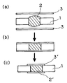
- a copper foil (CCL) 16 having a resin-coated layer 15 is arranged on both surfaces of the substrate 10 with the resin layer 15 facing the substrate 10, and (b) pressing is performed.
- the former has a possibility that the base material may be stretched after paste polishing, and there is a limit to thinning the film. Also, when lid plating is performed, the copper foil on the surface becomes thick and fine patterning becomes difficult. It was. On the other hand, the latter has a problem that a via hole (stacked via) cannot be provided on the via hole, a problem of insufficient smoothness of the substrate surface, crack generation during a long-term reliability test, and the like.
- a method of obtaining inner layer conduction only with a conductive paste without using through-hole plating or lid plating as described above has been used.
- conductive powder and conductive A press method using a paste that expresses conductivity when contacted with powder (hereinafter referred to as a powder contact paste) is used.
- a powder contact paste a paste that expresses conductivity when contacted with powder
- the paste is used under normal pressing conditions.
- the substrate immediately above swells and unevenness occurs, and there is also a problem that the rate of change in conductivity over time is large and the long-term reliability is poor.
- alloy-type paste a paste containing metal powder that is alloyed by heating
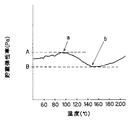
- the method for producing a multilayer substrate according to the present invention includes a step of drilling a via hole in a prepreg by laser processing, a step of filling the via hole with a conductive paste containing a resin component and metal powder, and the filled conductive material. And a step of arranging and pressing copper foil or a patterned copper foil portion of the base material on and under the conductive paste, and at least a part of the metal powder is melted as the conductive paste Using an alloy type paste in which adjacent metal powders are alloyed, as a prepreg, the storage elastic modulus at the inflection point at which the storage elastic modulus changes from increase to decrease in the temperature profile rising from 60 ° C.
- This prepreg has a ratio A / B of 10 or more before preheating when the storage elastic modulus at the inflection point changing from decrease to increase is B. It shall be less than 10 the ratio A / B by preheating before the perforation step.
- the prepreg one containing at least one of phenoxy resin, epoxy resin and bismaleide triazine resin (BT resin) can be used.
- alloying between metal powders means that two or more kinds of metals are melted and integrated. For example, when a mixture of low melting point metal particles and high melting point metal particles is heated, the surface layer of each particle is melted and integrated to form an alloy layer.
- the multilayer substrate obtained by the manufacturing method of the present invention does not use lid plating, and therefore fine line patterning is possible, satisfying the demand for thin plate.
- the metal powder contained in the conductive paste is alloyed, and the metal powder and the end face of the conductive layer in the through hole are alloyed, so that the conductivity and its long-term stability are excellent.
- a general-purpose prepreg can be used, which is advantageous in terms of cost.
- a stacked via structure can also be formed.
- the time required for the ratio A / B to be less than 10 is confirmed in advance, and before the step of providing the via hole by the laser processing, sandwiched between smooth surface plates, an air oven or the like under predetermined conditions confirmed in advance. You can heat with.
- the conductive paste used in the present invention contains at least a resin component and a metal powder. When heated at a predetermined temperature, the resin component hardens and at least a part of the metal powder melts to form a metal powder. What is necessary is just to be alloyed with each other or the metal powder and the conductive end face such as a copper foil or a patterned copper portion in contact therewith.
- the (A) resin component may be a blend of one or more resin components of alkyd resin, melamine resin, or xylene resin with acrylate resin monomer and epoxy resin prepolymer.
- the alkyd resin, melamine resin, and xylene resin are used as resin modifiers, respectively, and are not particularly limited as long as the purpose can be achieved.
- the blending ratio when blending these modifiers is less than 40% by weight, preferably less than 10% by weight, based on the total amount of component (A).
- Any metal powder may be used as long as it is alloyed by heating, but two or more metals including one or more low melting point metals having a melting point of 180 ° C. or less and one or more high melting point metals having a melting point of 800 ° C. or more are used. It is preferably included. Examples of the presence form of two or more metals include a mixture of a certain type of metal powder with a metal powder composed of another type of metal, or a type of metal powder coated with another type of metal, Or what mixed these is mentioned.
- the shape of the metal powder is not limited, but conventionally used ones such as dendrites, spheres, and flakes can be used.
- the particle size is not limited, but is usually about 1 to 50 ⁇ m in average particle size.
- the curing agent can be used in combination with a phenolic curing agent as an essential component, in addition to an imidazole curing agent, a cationic curing agent, a radical curing agent (polymerization initiator), and the like.
- the amount of phenolic curing agent used is preferably 0.3 to 35 parts with respect to 100 parts of the resin component.
- the amount of the curing agent other than the phenol-based curing agent is preferably 0.2 to 35 parts with respect to 100 parts of the resin, and preferably 0.5 to 40 parts for the entire curing agent.
- Examples of cationic curing agents include amine salts of boron trifluoride, P-methoxybenzenediazonium hexafluorophosphate, diphenyliodonium hexafluorophosphate, triphenylsulfonium, tetra-n-butylphosphonium tetraphenylborate, tetra- Examples thereof include onium compounds represented by n-butylphosphonium-o, o-diethyl phosphorodithioate and the like.
- Examples of radical curing agents (polymerization initiators) include di-cumyl peroxide, t-butyl cumyl peroxide, t-butyl hydroperoxide, cumene hydroperoxide, and the like.
- the flux as the component (D) promotes alloying of the metal powder examples include zinc chloride, lactic acid, citric acid, oleic acid, stearic acid, glutamic acid, benzoic acid, oxalic acid, Examples include glutamic acid hydrochloride, aniline hydrochloride, cetylpyridine bromide, urea, triethanolamine, glycerin, hydrazine, and rosin.
- the amount of flux used is preferably 0.3 to 80 parts with respect to 100 parts of the resin component.
- the multilayer substrate of the present invention After filling the via hole of the preheated prepreg with the conductive paste, the multilayer substrate of the present invention can be obtained by heating while pressing under the conditions corresponding to the alloy type paste used.
- the obtained multilayer substrates can be jointed using the preheated prepreg defined in the present invention, and further multilayered. Since the multilayer substrate obtained by the present invention is excellent in long-term reliability and also in the reliability of the joint portion between multilayer substrates, it is also possible to manufacture a super-multilayer substrate of several tens layers, which has been difficult in the past, with a high yield. This is possible according to the invention.
- the prepreg was sandwiched between stainless steel plates having a thickness of 1.2 mm, and the heat treatment for the time shown in the table was performed in a thermostat set to the temperature shown in Table 1.
- the storage elastic modulus of the prepreg is measured at an inflection point a where the storage elastic modulus changes from increase to decrease in a temperature profile rising from 60 ° C. to 200 ° C. using Modular® Compact® Rheometer (MCR) 300 manufactured by Anton® Paar.
- MCR Modular® Compact® Rheometer
- the elastic modulus A and the storage elastic modulus B at the inflection point b that changes from decrease to increase are measured before preheating and after preheating (except for Comparative Examples 1 and 2), and the ratio A / B is determined from these measured values. Asked.
- the following alloy type paste or powder contact type paste was used as shown in Table 1. Alloy type: TATSUTA System Electronics Co., Ltd. metallized paste (MP series) Powder contact type: TATSUTA System Electronics Co., Ltd., AE1840
Landscapes
- Engineering & Computer Science (AREA)
- Microelectronics & Electronic Packaging (AREA)
- Manufacturing & Machinery (AREA)
- Physics & Mathematics (AREA)
- Chemical & Material Sciences (AREA)
- Dispersion Chemistry (AREA)
- Spectroscopy & Molecular Physics (AREA)
- Production Of Multi-Layered Print Wiring Board (AREA)
- Conductive Materials (AREA)
- Printing Elements For Providing Electric Connections Between Printed Circuits (AREA)
- Parts Printed On Printed Circuit Boards (AREA)
Abstract
Description
表1に示した厚さ約100μmのプリプレグ(パナソニック電工(株)製R-1551又は三菱ガス化学(株)製GHPL-830)をそれぞれ用い、実施例1~3,比較例3では下記の通り予備加熱し、比較例1,2では予備加熱を行わなかった。これらのプリプレグにCO2レーザーを用いて、φ100μm、φ150μmの孔を設け、印刷法により表1に示した導電性ペーストを充填した後、真空プレス機を用いて次の条件でプレスを行った。
温度:30℃→130℃(昇温17分、保持10分)→180℃(昇温24分、保持46分)→30℃(冷却23分)
合金型:タツタ システム・エレクトロニクス(株)製、メタライズペースト(MPシリーズ)
粉体接触型:タツタ システム・エレクトロニクス(株)製、AE1840
上記により得られた多層基板につき、以下の評価を行った。
完成基板の断面を光学顕微鏡で観察し、図6に示す膨れ量(s)を測定し、5μm未満を○、5μm以上を×とした。
φ0.15mmの初期導電性については、200孔、400孔、600孔、800孔連結パターンを作製し、抵抗値を測定した。それらを各孔数で除算し、1孔当たりの抵抗値を求め、その平均値を算出した。200孔、400孔、600孔連結パターン作製はN=6で行い、800孔連結パターン作製はN=2で行った。
作製した任意の連結パターンにおいて試験前に測定した抵抗値をa、試験後に測定した抵抗値をbとして、導電性変化率を次式により求め、導電性変化率が±20%以内であった場合を○、-20%未満又は20%を越えた場合を×とした。
(b-a)×100/a
半田ディップ試験:260℃の半田に10秒間浸漬した後常温大気で冷却するサイクルを3サイクル繰り返した。
プレッシャークッカーテスト(PCT):121℃、湿度100%、2気圧の雰囲気に24時間暴露した。
ヒートサイクル試験:-65℃で30分間保持した後、125℃で30分間保持するサイクルを1000サイクル繰り返す雰囲気に暴露した。
耐熱性試験:100℃の雰囲気で1000時間暴露した。
耐湿性試験:温度85℃、湿度85%の雰囲気で1000時間暴露した。
φ150μmの孔に導電性ペーストを充填し、孔ピッチが0.6mm、0.8mm、1.0mmの3種のピッチとなるように櫛形パターンを作製した。そのパターンに直流電流50Vを印加し、温度85℃、湿度85%で1000時間暴露後、試験雰囲気のまま抵抗値を測定し、その抵抗値が106Ω以上の場合を○、106Ω未満の場合を×とした。

10……コア基板、11……銅箔層、12……スルーホールメッキ
13……導電性ペースト、14……蓋メッキ、15……樹脂層、16……銅箔
Claims (6)
- プリプレグにレーザー加工にてビアホールを設ける穿孔工程と、そのビアホールに樹脂構成成分と金属粉とを含有する導電性ペーストを充填する工程と、その充填された導電性ペーストの上下に銅箔又はパターニングされた基材の銅箔部分を配してプレスする工程とを含む多層基板の製造方法であって、
前記導電性ペーストとして前記金属粉の少なくとも一部が溶融して隣接する金属粉同士が合金化する合金型ペーストを用い、
前記プリプレグとして、60℃から200℃へ昇温する温度プロファイルにおいて貯蔵弾性率が増加から減少に変化する変曲点における貯蔵弾性率をA、減少から増加に変わる変曲点における貯蔵弾性率をBとした場合の比率A/Bが予備加熱前に10以上であるものを用い、
該プリプレグを前記穿孔工程前に予備加熱することにより前記比率A/Bを10未満にする
ことを特徴とする多層配線基板の製造方法。 - 前記プリプレグとして、フェノキシ樹脂、エポキシ樹脂及びビスマレイドトリアジン樹脂のうちの少なくとも1種を含有してなるものを用いることを特徴とする、請求項1に記載の多層配線基板の製造方法。
- 前記予備加熱を80~140℃で30~120分間行うことを特徴とする、請求項1又は2に記載の多層配線基板の製造方法。
- 前記導電性ペーストとして以下の組成を有するものを使用することを特徴とする、請求項1~3のいずれか1項に記載の多層配線基板の製造方法;
(A)アクリレート樹脂モノマー及びエポキシ樹脂プレポリマーを含む樹脂構成成分100重量部に対し、
(B)インジウム単独、又は錫、鉛、ビスマス及びインジウムからなる群から選択された2種以上の合金である融点180℃以下の低融点金属少なくとも1種と、金、銀、銅、及びニッケルからなる群から選択された少なくとも1種の金属及び/又はこの群から選択された2種以上の金属の合金である融点800℃以上の高融点金属とを含む金属粉200~2200重量部、
(C)フェノール系硬化剤0.3~35重量部を含む硬化剤0.5~40重量部、及び
(D)フラックス0.3~80重量部。 - 請求項1~4のいずれか1項に記載の製造方法により製造された多層配線基板。
- プリプレグにビアホールを設け、このビアホールに導電性ペーストを充填して、その充填された導電性ペーストの上下に銅箔又はパターニングされた基材の銅箔部分を配してなる多層配線基板であって、
前記プリプレグとして、60℃から200℃へ昇温する温度プロファイルにおいて貯蔵弾性率が増加から減少に変化する変曲点における貯蔵弾性率をA、減少から増加に変わる変曲点における貯蔵弾性率をBとした場合の比率A/Bが10未満であるものを用い、
前記導電性ペーストとして、加熱により相互に合金化する2種以上の金属からなる金属粉を含むものを用いた
ことを特徴とする多層配線基板。
Priority Applications (7)
| Application Number | Priority Date | Filing Date | Title |
|---|---|---|---|
| HK12108404.9A HK1167776B (en) | 2009-03-12 | 2010-03-09 | Multilayer wiring substrate producing method and multilayer wiring substrate obtained by the same |
| KR1020117021603A KR101114058B1 (ko) | 2009-03-12 | 2010-03-09 | 다층 배선 기판의 제조 방법과 이에 의해 수득되는 다층 배선 기판 |
| CN2010800115999A CN102369791B (zh) | 2009-03-12 | 2010-03-09 | 多层配线基板的制造方法及通过该方法获得的多层配线基板 |
| EP10750562.0A EP2408285B1 (en) | 2009-03-12 | 2010-03-09 | Method of manufacturing multilayer printed wiring board and multilayer wiring board obtained thereby |
| JP2010525547A JP4778114B2 (ja) | 2009-03-12 | 2010-03-09 | 多層配線基板の製造方法及びそれにより得られる多層配線基板 |
| US13/256,114 US8756805B2 (en) | 2009-03-12 | 2010-03-09 | Method of manufacturing multilayer printed wiring board |
| US14/164,900 US9420706B2 (en) | 2009-03-12 | 2014-01-27 | Multilayer wiring board |
Applications Claiming Priority (4)
| Application Number | Priority Date | Filing Date | Title |
|---|---|---|---|
| JP2009-059375 | 2009-03-12 | ||
| JP2009059375 | 2009-03-12 | ||
| JP2009171229 | 2009-07-22 | ||
| JP2009-171229 | 2009-07-22 |
Related Child Applications (2)
| Application Number | Title | Priority Date | Filing Date |
|---|---|---|---|
| US13/256,114 A-371-Of-International US8756805B2 (en) | 2009-03-12 | 2010-03-09 | Method of manufacturing multilayer printed wiring board |
| US14/164,900 Division US9420706B2 (en) | 2009-03-12 | 2014-01-27 | Multilayer wiring board |
Publications (1)
| Publication Number | Publication Date |
|---|---|
| WO2010103805A1 true WO2010103805A1 (ja) | 2010-09-16 |
Family
ID=42728101
Family Applications (1)
| Application Number | Title | Priority Date | Filing Date |
|---|---|---|---|
| PCT/JP2010/001656 Ceased WO2010103805A1 (ja) | 2009-03-12 | 2010-03-09 | 多層配線基板の製造方法及びそれにより得られる多層配線基板 |
Country Status (7)
| Country | Link |
|---|---|
| US (2) | US8756805B2 (ja) |
| EP (1) | EP2408285B1 (ja) |
| JP (1) | JP4778114B2 (ja) |
| KR (1) | KR101114058B1 (ja) |
| CN (1) | CN102369791B (ja) |
| TW (1) | TWI419633B (ja) |
| WO (1) | WO2010103805A1 (ja) |
Cited By (3)
| Publication number | Priority date | Publication date | Assignee | Title |
|---|---|---|---|---|
| EP2563103A4 (en) * | 2011-01-18 | 2013-05-15 | Panasonic Corp | CIRCUIT SUBSTRATE, METHOD FOR PRODUCING THE CIRCUIT SUBSTRATE AND CONTINUOUS PASTE THEREFOR |
| JP2016089191A (ja) * | 2014-10-30 | 2016-05-23 | 国立研究開発法人産業技術総合研究所 | レーザ照射による金属粉末を用いた金属造形物作成法、そのための形成材料、及び作成された構造体 |
| WO2025254165A1 (ja) * | 2024-06-04 | 2025-12-11 | 株式会社フジクラ | プリント配線板 |
Families Citing this family (6)
| Publication number | Priority date | Publication date | Assignee | Title |
|---|---|---|---|---|
| JP5693940B2 (ja) | 2010-12-13 | 2015-04-01 | 株式会社トクヤマ | セラミックスビア基板、メタライズドセラミックスビア基板、これらの製造方法 |
| KR20130066929A (ko) * | 2011-12-13 | 2013-06-21 | 한국전자통신연구원 | 패턴 형성 조성물 및 이를 이용한 패턴 형성 방법 |
| WO2013096846A1 (en) * | 2011-12-21 | 2013-06-27 | Lawrence Livermore National Security, Llc | Method of fabricating electrical feedthroughs using extruded metal vias |
| US10263320B2 (en) * | 2015-07-17 | 2019-04-16 | Ohio State Innovation Foundation | Methods of making stretchable and flexible electronics |
| CN110088895B (zh) * | 2016-12-28 | 2023-05-23 | 拓自达电线株式会社 | 散热基材、散热电路结构体及其制造方法 |
| CN111491458A (zh) * | 2019-01-25 | 2020-08-04 | 鹏鼎控股(深圳)股份有限公司 | 电路板及其制作方法 |
Citations (5)
| Publication number | Priority date | Publication date | Assignee | Title |
|---|---|---|---|---|
| JPH07176846A (ja) | 1993-10-29 | 1995-07-14 | Matsushita Electric Ind Co Ltd | ビアホール充填用導体ペースト組成物並びにそれを用いた両面及び多層プリント基板とその製造方法 |
| JP2002232147A (ja) * | 2001-01-31 | 2002-08-16 | Purintekku:Kk | 多層配線板およびその製造方法 |
| JP2007019198A (ja) * | 2005-07-07 | 2007-01-25 | Fujitsu Ltd | 積層基板および該積層基板を有する電子機器 |
| JP2008243391A (ja) * | 2007-03-26 | 2008-10-09 | Mitsubishi Plastics Ind Ltd | ビアホール充填用導電性ペースト組成物とそれを用いた多層配線基板 |
| JP4191678B2 (ja) | 2002-05-31 | 2008-12-03 | タツタ電線株式会社 | 導電性ペースト、これを用いた多層基板及びその製造方法 |
Family Cites Families (17)
| Publication number | Priority date | Publication date | Assignee | Title |
|---|---|---|---|---|
| US4544801A (en) * | 1982-06-28 | 1985-10-01 | International Business Machines Corporation | Circuit board including multiple wire photosensitive adhesive |
| JPH04191678A (ja) | 1990-11-27 | 1992-07-09 | Toshiba Corp | 集積回路検査装置 |
| US5403869A (en) * | 1992-08-17 | 1995-04-04 | Hitachi Chemical Company, Ltd. | Adhesive of epoxy resins, epoxy-modified polybutadiene and photoinitiator |
| CA2196024A1 (en) * | 1996-02-28 | 1997-08-28 | Craig N. Ernsberger | Multilayer electronic assembly utilizing a sinterable composition and related method of forming |
| JPH1072752A (ja) * | 1996-05-15 | 1998-03-17 | Matsushita Electric Ind Co Ltd | プリント配線板用不織布基材とこれを用いたプリプレグ |
| JP2002329974A (ja) * | 2001-05-01 | 2002-11-15 | Nitto Denko Corp | 配線基板及びその製造方法 |
| JP2004002789A (ja) * | 2002-04-03 | 2004-01-08 | Sekisui Chem Co Ltd | 離型フィルム、積層離型フィルム及び基板の製造方法 |
| JP2004158651A (ja) * | 2002-11-06 | 2004-06-03 | Murata Mfg Co Ltd | 樹脂基板の製造方法、樹脂多層基板の製造方法、および樹脂基板 |
| JP4747707B2 (ja) * | 2004-11-09 | 2011-08-17 | ソニー株式会社 | 多層配線基板及び基板製造方法 |
| WO2006080073A1 (ja) * | 2005-01-27 | 2006-08-03 | Matsushita Electric Industrial Co., Ltd. | 多層回路基板の製造方法、多層回路基板 |
| WO2006118059A1 (ja) * | 2005-04-27 | 2006-11-09 | Hitachi Chemical Company, Ltd. | 複合体、プリプレグ、金属箔張積層板、回路基板接続材、並びに、多層プリント配線板及びその製造方法 |
| TW200740334A (en) * | 2005-10-20 | 2007-10-16 | Matsushita Electric Industrial Co Ltd | Multilayer printed wiring board and its manufacturing method |
| JP2007161797A (ja) * | 2005-12-12 | 2007-06-28 | Matsushita Electric Ind Co Ltd | プリプレグの特性試験方法 |
| WO2007069510A1 (ja) * | 2005-12-12 | 2007-06-21 | Matsushita Electric Industrial Co., Ltd. | 回路基板を製造するための中間材とそれを用いた回路基板の製造方法 |
| JP5109283B2 (ja) * | 2006-04-20 | 2012-12-26 | パナソニック株式会社 | 回路基板の製造方法 |
| JP5214154B2 (ja) * | 2007-01-19 | 2013-06-19 | 住友電気工業株式会社 | プリント配線板およびその製造方法 |
| JP2008205111A (ja) * | 2007-02-19 | 2008-09-04 | Fujitsu Ltd | 配線基板および半導体装置、配線基板の製造方法 |
-
2010
- 2010-03-09 EP EP10750562.0A patent/EP2408285B1/en not_active Not-in-force
- 2010-03-09 CN CN2010800115999A patent/CN102369791B/zh active Active
- 2010-03-09 JP JP2010525547A patent/JP4778114B2/ja active Active
- 2010-03-09 WO PCT/JP2010/001656 patent/WO2010103805A1/ja not_active Ceased
- 2010-03-09 US US13/256,114 patent/US8756805B2/en active Active
- 2010-03-09 KR KR1020117021603A patent/KR101114058B1/ko active Active
- 2010-03-10 TW TW099106904A patent/TWI419633B/zh active
-
2014
- 2014-01-27 US US14/164,900 patent/US9420706B2/en active Active
Patent Citations (5)
| Publication number | Priority date | Publication date | Assignee | Title |
|---|---|---|---|---|
| JPH07176846A (ja) | 1993-10-29 | 1995-07-14 | Matsushita Electric Ind Co Ltd | ビアホール充填用導体ペースト組成物並びにそれを用いた両面及び多層プリント基板とその製造方法 |
| JP2002232147A (ja) * | 2001-01-31 | 2002-08-16 | Purintekku:Kk | 多層配線板およびその製造方法 |
| JP4191678B2 (ja) | 2002-05-31 | 2008-12-03 | タツタ電線株式会社 | 導電性ペースト、これを用いた多層基板及びその製造方法 |
| JP2007019198A (ja) * | 2005-07-07 | 2007-01-25 | Fujitsu Ltd | 積層基板および該積層基板を有する電子機器 |
| JP2008243391A (ja) * | 2007-03-26 | 2008-10-09 | Mitsubishi Plastics Ind Ltd | ビアホール充填用導電性ペースト組成物とそれを用いた多層配線基板 |
Non-Patent Citations (1)
| Title |
|---|
| See also references of EP2408285A4 |
Cited By (3)
| Publication number | Priority date | Publication date | Assignee | Title |
|---|---|---|---|---|
| EP2563103A4 (en) * | 2011-01-18 | 2013-05-15 | Panasonic Corp | CIRCUIT SUBSTRATE, METHOD FOR PRODUCING THE CIRCUIT SUBSTRATE AND CONTINUOUS PASTE THEREFOR |
| JP2016089191A (ja) * | 2014-10-30 | 2016-05-23 | 国立研究開発法人産業技術総合研究所 | レーザ照射による金属粉末を用いた金属造形物作成法、そのための形成材料、及び作成された構造体 |
| WO2025254165A1 (ja) * | 2024-06-04 | 2025-12-11 | 株式会社フジクラ | プリント配線板 |
Also Published As
| Publication number | Publication date |
|---|---|
| CN102369791B (zh) | 2013-11-13 |
| HK1167776A1 (en) | 2012-12-07 |
| JP4778114B2 (ja) | 2011-09-21 |
| TW201043109A (en) | 2010-12-01 |
| TWI419633B (zh) | 2013-12-11 |
| US20140138126A1 (en) | 2014-05-22 |
| JPWO2010103805A1 (ja) | 2012-09-13 |
| US8756805B2 (en) | 2014-06-24 |
| CN102369791A (zh) | 2012-03-07 |
| EP2408285B1 (en) | 2018-11-14 |
| US9420706B2 (en) | 2016-08-16 |
| KR20110112877A (ko) | 2011-10-13 |
| US20120037409A1 (en) | 2012-02-16 |
| EP2408285A1 (en) | 2012-01-18 |
| EP2408285A4 (en) | 2017-11-22 |
| KR101114058B1 (ko) | 2012-03-13 |
Similar Documents
| Publication | Publication Date | Title |
|---|---|---|
| JP4778114B2 (ja) | 多層配線基板の製造方法及びそれにより得られる多層配線基板 | |
| JP4191678B2 (ja) | 導電性ペースト、これを用いた多層基板及びその製造方法 | |
| JP5333701B1 (ja) | 配線基板とその製造方法 | |
| JP5333702B1 (ja) | フレキシブル配線基板とその製造方法と、これを用いた実装製品と、フレキシブル多層配線基板 | |
| JP5344022B2 (ja) | エポキシ樹脂組成物、プリプレグ、積層板、樹脂シート、プリント配線板及び半導体装置 | |
| JP5381869B2 (ja) | エポキシ樹脂前駆体組成物、プリプレグ、積層板、樹脂シート、プリント配線板および半導体装置 | |
| JP5064842B2 (ja) | 金属箔、それを用いた金属ベース回路基板、金属ベース多層回路基板の製造方法 | |
| JP2009194105A (ja) | スルーホール用充填剤及び多層配線基板 | |
| JP5293654B2 (ja) | 回路基板用樹脂組成物、プリプレグ、積層板、プリント配線板、及び半導体装置 | |
| WO2023282351A1 (ja) | 導電性ペースト、及びこれを用いた多層基板 | |
| JP4481734B2 (ja) | 多層配線基板用導電性ペースト組成物 | |
| JP4965102B2 (ja) | ビアホール充填用導電性ペースト組成物 | |
| HK1167776B (en) | Multilayer wiring substrate producing method and multilayer wiring substrate obtained by the same | |
| JPH01244849A (ja) | 電気積層板の製造方法 | |
| JP2005101163A (ja) | プリプレグならびにこれを用いたプリント配線板用積層板およびプリント配線板 | |
| JP5417071B2 (ja) | 回路基板 | |
| JP2011144229A (ja) | シアネート樹脂組成物、プリプレグ、積層板、プリント配線板、及び半導体装置 | |
| WO2013099204A1 (ja) | 配線基板とその製造方法 | |
| JP2001320165A (ja) | 両面及び多層プリント配線板の製造方法 | |
| JPH0466181B2 (ja) | ||
| JP2011241345A (ja) | エポキシ樹脂組成物、プリプレグ、金属張積層板、プリント配線板及び半導体装置 |
Legal Events
| Date | Code | Title | Description |
|---|---|---|---|
| WWE | Wipo information: entry into national phase |
Ref document number: 201080011599.9 Country of ref document: CN |
|
| WWE | Wipo information: entry into national phase |
Ref document number: 2010525547 Country of ref document: JP |
|
| 121 | Ep: the epo has been informed by wipo that ep was designated in this application |
Ref document number: 10750562 Country of ref document: EP Kind code of ref document: A1 |
|
| NENP | Non-entry into the national phase |
Ref country code: DE |
|
| ENP | Entry into the national phase |
Ref document number: 20117021603 Country of ref document: KR Kind code of ref document: A |
|
| WWE | Wipo information: entry into national phase |
Ref document number: 2010750562 Country of ref document: EP |
|
| WWE | Wipo information: entry into national phase |
Ref document number: 13256114 Country of ref document: US |