WO2010103902A1 - Dispositif à élément électroluminescent à semi-conducteurs - Google Patents
Dispositif à élément électroluminescent à semi-conducteurs Download PDFInfo
- Publication number
- WO2010103902A1 WO2010103902A1 PCT/JP2010/052502 JP2010052502W WO2010103902A1 WO 2010103902 A1 WO2010103902 A1 WO 2010103902A1 JP 2010052502 W JP2010052502 W JP 2010052502W WO 2010103902 A1 WO2010103902 A1 WO 2010103902A1
- Authority
- WO
- WIPO (PCT)
- Prior art keywords
- semiconductor light
- wavelength conversion
- conversion member
- emitting element
- light emitting
- Prior art date
- Legal status (The legal status is an assumption and is not a legal conclusion. Google has not performed a legal analysis and makes no representation as to the accuracy of the status listed.)
- Ceased
Links
Images


Classifications
-
- H—ELECTRICITY
- H10—SEMICONDUCTOR DEVICES; ELECTRIC SOLID-STATE DEVICES NOT OTHERWISE PROVIDED FOR
- H10H—INORGANIC LIGHT-EMITTING SEMICONDUCTOR DEVICES HAVING POTENTIAL BARRIERS
- H10H20/00—Individual inorganic light-emitting semiconductor devices having potential barriers, e.g. light-emitting diodes [LED]
- H10H20/80—Constructional details
- H10H20/85—Packages
- H10H20/851—Wavelength conversion means
- H10H20/8516—Wavelength conversion means having a non-uniform spatial arrangement or non-uniform concentration, e.g. patterned wavelength conversion layer or wavelength conversion layer with a concentration gradient
-
- H—ELECTRICITY
- H10—SEMICONDUCTOR DEVICES; ELECTRIC SOLID-STATE DEVICES NOT OTHERWISE PROVIDED FOR
- H10H—INORGANIC LIGHT-EMITTING SEMICONDUCTOR DEVICES HAVING POTENTIAL BARRIERS
- H10H20/00—Individual inorganic light-emitting semiconductor devices having potential barriers, e.g. light-emitting diodes [LED]
- H10H20/80—Constructional details
- H10H20/85—Packages
- H10H20/851—Wavelength conversion means
- H10H20/8515—Wavelength conversion means not being in contact with the bodies
-
- H—ELECTRICITY
- H10—SEMICONDUCTOR DEVICES; ELECTRIC SOLID-STATE DEVICES NOT OTHERWISE PROVIDED FOR
- H10W—GENERIC PACKAGES, INTERCONNECTIONS, CONNECTORS OR OTHER CONSTRUCTIONAL DETAILS OF DEVICES COVERED BY CLASS H10
- H10W90/00—Package configurations
- H10W90/701—Package configurations characterised by the relative positions of pads or connectors relative to package parts
- H10W90/751—Package configurations characterised by the relative positions of pads or connectors relative to package parts of bond wires
- H10W90/756—Package configurations characterised by the relative positions of pads or connectors relative to package parts of bond wires between a chip and a stacked lead frame, conducting package substrate or heat sink
Definitions
- the present invention relates to a semiconductor light-emitting element device for converting a part of light emitted from a semiconductor light-emitting element such as an LED (light-emitting diode) or LD (laser diode) into another wavelength and mainly irradiating white light. Is.
- a semiconductor light-emitting element such as an LED (light-emitting diode) or LD (laser diode) into another wavelength and mainly irradiating white light. Is.
- a white LED has a structure in which a mixture of an inorganic phosphor powder and a resin is coated and molded on an excitation LED chip.
- the resin used for the coating mold is easily colored or deformed. Therefore, there is a problem that the emission color changes in a short period of time and the life as a semiconductor light emitting element device is shortened. This problem is considered to be serious with the increase in output of the LED chip, and the development of a semiconductor light emitting element device having excellent heat resistance has been desired.
- an LED device using a wavelength conversion member made of a completely inorganic solid that does not use a resin has been proposed (for example, see Patent Document 1). Since the wavelength conversion member does not use a resin having poor heat resistance and is made of a completely inorganic solid, it has excellent heat resistance and hardly undergoes thermal degradation.
- the wavelength conversion member disclosed in Patent Document 1 is provided, for example, as a plate-shaped molded body by filling a mold with a mixture of glass powder and inorganic phosphor powder and heat-treating (sintering) near the softening point.
- FIG. 8 shows a conventional semiconductor light emitting element device using a plate-like wavelength conversion member.
- the semiconductor light emitting element 3 is electrically connected to a lead electrode (not shown) on the substrate 2 using a bonding wire 5.
- the bonding wire 5 obstructs the approach between the wavelength conversion member 4 and the semiconductor light emitting element 3, thereby reducing the degree of mounting freedom.
- the distance D between the semiconductor light emitting element 3 and the wavelength conversion member 4 is increased, the light emitted from the semiconductor light emitting element 3 is attenuated before entering the wavelength conversion member 4, so that the light flux value is reduced. There is also a problem.
- the bonding wire 5 since the bonding wire 5 exists between the semiconductor light emitting element 3 and the wavelength conversion member 4, the bonding wire 5 absorbs the light emitted from the semiconductor light emitting element 3, or the shadow of the bonding wire 5 is changed to the wavelength conversion member. There is also a problem that the luminous flux value is lowered due to projection onto the image.
- an object of the present invention is to provide a semiconductor light-emitting element device that is mounted using a bonding wire and has a low decrease in luminous flux value.
- the present inventors have found that the above problem can be solved by having a semiconductor light-emitting element device mounted using a bonding wire having a specific structure, and propose the present invention. is there.
- the present invention provides a semiconductor light emitting device, a bonding wire that electrically connects the semiconductor light emitting device and the lead electrode, and a wavelength of a part of light emitted from the semiconductor light emitting device that is disposed above the semiconductor light emitting device.
- a wavelength conversion member for conversion wherein the wavelength conversion member has an opening and / or a notch, and at least a part of the bonding wire includes the opening and / or Or it is related with the semiconductor light-emitting device characterized by penetrating the notch part.
- the bonding wire hinders the proximity of the wavelength conversion member and the semiconductor light-emitting device. There was a problem of doing.
- the configuration of the present invention since the bonding wire penetrates the opening and / or the notch formed in the wavelength conversion member, the wavelength conversion member is closer to the semiconductor light emitting device. It becomes possible to make it.
- the degree of freedom of mounting on the package is improved, and light emitted from the semiconductor light emitting element is efficiently incident on the wavelength conversion member, so that the light flux value can be increased.
- the problem of light absorption of the bonding wire and the projection of the shadow of the bonding wire onto the wavelength conversion member can be greatly improved.
- the distance between the wavelength conversion member and the semiconductor light emitting device is preferably 800 ⁇ m or less.
- the light emitted from the semiconductor light emitting element can be efficiently incident on the wavelength conversion member, so that it is easy to enjoy the effect of increasing the luminous flux value.
- the opening and / or the notch is formed by laser processing.
- the wavelength conversion member has an opening and / or a notch that is larger than necessary, the wavelength conversion loss of the light emitted from the semiconductor light emitting element will result. As a result, the conversion efficiency is lowered, and there is a possibility that light of a desired color cannot be obtained. Therefore, the opening and / or the cutout portion of the wavelength conversion member may be at least as long as the bonding wire can penetrate. In this case, if the laser beam is used, the wavelength conversion member can be finely processed, so that a fine opening and / or notch can be formed in the wavelength conversion member. Therefore, it is possible to obtain a semiconductor light emitting element device with high conversion efficiency.
- a bonding wire having a diameter of about 50 ⁇ m or less is used for mounting a semiconductor light emitting element device, but according to laser processing, an opening having a diameter of 100 ⁇ m or less, which was impossible with a conventional cutting tool, is formed. It becomes possible.
- the wavelength conversion member is made of a sintered product of mixed powder containing glass powder and inorganic phosphor powder.
- the wavelength conversion member is made of a completely inorganic solid obtained by firing a mixed powder of glass powder and inorganic phosphor powder, thereby providing superior heat resistance compared to a resin wavelength conversion member. And is less susceptible to thermal degradation. Specifically, by dispersing the inorganic phosphor powder in the glass, the effect of protecting the inorganic phosphor powder is enhanced, and at the same time, the glass is heated compared to a resin material such as an epoxy resin or a silicone resin. Since the durability against ultraviolet rays is high, the life of the wavelength conversion member can be extended.
- the present invention is a wavelength conversion member that is used by being installed above a semiconductor light emitting element in a semiconductor light emitting element device, and converts the wavelength of a part of the light emitted by the semiconductor light emitting element.
- the present invention relates to a wavelength conversion member characterized in that an opening and / or a notch for penetrating a bonding wire that electrically connects an element and a lead electrode is formed.
- the wavelength conversion member of the present invention can enjoy the effects as described above when used for a semiconductor light-emitting element device mounted using a bonding wire.
- the wavelength conversion member of the present invention is characterized in that the opening and / or the notch is formed by laser processing.
- the wavelength conversion member of the present invention is characterized by comprising a sintered product of a mixed powder containing glass powder and inorganic phosphor powder.
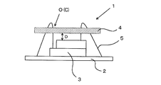
- FIG. 1 is a cross-sectional view showing a first embodiment of the semiconductor light-emitting device of the present invention.
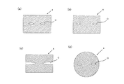
- Fig.2 (a) is a top view which shows 1st embodiment of the wavelength conversion member used for the semiconductor light-emitting device of FIG.
- FIG.2 (b) is a top view which shows 2nd embodiment of the wavelength conversion member used for the semiconductor light-emitting device of FIG.
- FIG.2 (c) is a top view which shows 3rd embodiment of the wavelength conversion member used for the semiconductor light-emitting device of FIG.
- FIG.2 (d) is a top view which shows 4th embodiment of the wavelength conversion member used for the semiconductor light-emitting device of FIG.
- FIG.2 (a) is a top view which shows 1st embodiment of the wavelength conversion member used for the semiconductor light-emitting device of FIG.
- FIG.2 (b) is a top view which shows 2nd embodiment of the wavelength conversion member used for the semiconductor light-emitting device of FIG.
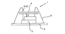
- FIG. 3 is a cross-sectional view showing a second embodiment of the semiconductor light emitting device of the present invention.
- Fig.4 (a) is a top view which shows 1st embodiment of the wavelength conversion member used for the semiconductor light-emitting device of FIG.
- FIG. 4B is a plan view showing a second embodiment of the wavelength conversion member used in the semiconductor light emitting device of FIG.
- FIG.4 (c) is a top view which shows 3rd embodiment of the wavelength conversion member used for the semiconductor light-emitting device of FIG.
- FIG. 5 is a cross-sectional view showing a third embodiment of the semiconductor light emitting device of the present invention.
- Fig.6 (a) is a top view which shows 1st embodiment of the wavelength conversion member used for the semiconductor light-emitting device of FIG.
- FIG.6 (b) is a top view which shows 2nd embodiment of the wavelength conversion member used for the semiconductor light-emitting device of FIG.
- FIG.6 (c) is a top view which shows 3rd embodiment of the wavelength conversion member used for the semiconductor light-emitting device of FIG.
- FIG. 7 is a cross-sectional view showing a fourth embodiment of the semiconductor light emitting device according to the present invention.
- FIG. 8 is a cross-sectional view showing a conventional semiconductor light emitting device.
- FIG. 1 is a cross-sectional view of a first embodiment of a semiconductor light emitting device of the present invention
- FIG. 2 is a plan view showing a wavelength conversion member in the semiconductor light emitting device of FIG.
- the semiconductor light emitting element 3 is installed on a substrate 2 and is electrically connected to a lead electrode (not shown) on the substrate 2 by two arched bonding wires 5.
- a plate-like wavelength conversion member 4 is installed above the semiconductor light emitting element 3.
- the wavelength conversion member 4 is normally installed and used on a casing or a cup.
- the wavelength conversion member 4 is provided with an opening O or a notch C.
- the bonding wire 5 connected to the semiconductor light emitting element 3 once passes through the opening O or notch C, then bends in an arch shape on the wavelength conversion member 4, and again passes through the opening O or notch C. In this way, the lead electrode on the substrate 2 is connected.
- the planar shape of the wavelength conversion member 4 is a rectangle, and an elliptical shape through which each bonding wire 5 penetrates.
- One opening O is formed on each of the left and right sides.
- the top of the arch-shaped bonding wire 5 that connects the semiconductor light emitting element 3 and the lead electrode protrudes above the wavelength conversion member 4 at the opening O.
- the bonding wire 5 connected to the semiconductor light emitting element 3 passes through one of the openings O and protrudes onto the wavelength conversion member 4 and bends in an arch shape on the wavelength conversion member 4. It is the structure which penetrates this opening part O and is connected with a lead electrode.
- the semi-elliptical cutout portions C through which the bonding wires 5 pass are provided on the left and right sides, respectively. It is formed one by one.
- the top of the arch-shaped bonding wire 5 that connects the semiconductor light emitting element 3 and the lead electrode protrudes above the wavelength conversion member 4 at the notch C.
- the planar shape of the wavelength conversion member 4 is circular, and each bonding wire 5 is formed as in (a).
- An elliptical opening O for penetrating is formed on each of the left and right sides.
- FIG. 3 is a cross-sectional view of a second embodiment of the semiconductor light emitting device of the present invention
- FIG. 4 is a plan view of a wavelength conversion member in the semiconductor light emitting device of FIG.
- the two bonding wires 5 form an arch shape, and each bonding wire 5 protrudes above the wavelength conversion member 4 through one opening O or notch C. After being bent in an arch shape, the structure is connected to the lead electrode through the outside of the wavelength conversion member 4, that is, without penetrating the opening O and the notch C again.
- a circular opening O through which each bonding wire 5 penetrates is formed at one place on each side. ing.
- the triangular cutout portions C through which the bonding wires 5 penetrate are respectively formed in the upper left corner and the lower right corner. It is formed one by one.
- the rectangular cutouts C through which the bonding wires 5 pass are respectively formed in the upper left corner and the upper right corner. It is formed one by one.
- FIG. 5 is a cross-sectional view of a third embodiment of the semiconductor light emitting device of the present invention
- FIG. 6 is a plan view of a wavelength conversion member in the semiconductor light emitting device of FIG.
- one bonding wire 5 forms an arch shape
- the bonding wire 5 passes through the opening O or notch C formed in the wavelength conversion member 4 and above the wavelength conversion member 4. After being bent and bent in an arch shape, it is connected to the lead electrode through the outside of the wavelength conversion member 4, that is, without penetrating the opening O and the notch C again.
- the lower surface of the semiconductor light emitting element 3 is electrically connected to a lead electrode (not shown) formed on the substrate 2.
- one circular opening O through which the bonding wire 5 passes is formed.
- one semi-elliptical cutout portion C through which the bonding wire 5 passes is formed.
- a rectangular cutout C for allowing the bonding wire 5 to pass therethrough is formed at one place in the upper right corner. Yes.
- FIG. 7 is a cross-sectional view of a fourth embodiment of the semiconductor light emitting device of the present invention.
- the substrate 2 also serves as a reflector that reflects and collects light emitted from the semiconductor light emitting element 3 and light converted in wavelength by the wavelength conversion member 4.
- the semiconductor light emitting device 3 is installed at the bottom of the casing-like substrate 2 and is electrically connected to a lead electrode (not shown) on the substrate 2 and an external lead electrode 6 using bonding wires 5. .
- the wavelength conversion member 4 is installed above the semiconductor light emitting element 3.
- the wavelength conversion member 4 is provided with an opening O or a notch C (for example, (a) to (c) in FIG.
- the bonding wire 5 passes through the opening O or the notch C (a gap formed between the wavelength conversion member 4 and the casing-like substrate 2), protrudes above the wavelength conversion member 4, and bends in an arch shape. After that, the structure is connected to the lead electrode through the outside of the wavelength conversion member 4, that is, without penetrating the opening O and the notch C again.
- the semiconductor light-emitting element device of the present invention can reduce the distance between the semiconductor light-emitting element and the wavelength conversion member by the configuration as described above.
- the distance between the semiconductor light emitting element and the wavelength conversion member is preferably 800 ⁇ m or less, 500 ⁇ m or less, and particularly preferably 300 ⁇ m or less. Although a minimum is not specifically limited, For example, it adjusts suitably in 10 micrometers or more, especially 50 micrometers or more. Further, the semiconductor light emitting element and the wavelength conversion member may be in contact with each other. Note that the distance between the semiconductor light emitting element and the wavelength conversion member indicates a distance D between the upper surface of the semiconductor light emitting element 3 and the lower surface of the wavelength conversion member 4 as shown in FIG.
- the shape of the opening formed in the wavelength conversion member is not particularly limited, and may be a polygon such as a rectangle or a triangle other than a circle or an ellipse.
- the shape of the notch is not particularly limited, and is appropriately selected from a part of a circle (such as a semicircle), a part of an ellipse (such as a half ellipse), a polygon such as a triangle and a rectangle.
- the size of the opening and notch formed in the wavelength conversion member is preferably as small as possible from the viewpoint of light conversion efficiency.
- the diameter is preferably 100 ⁇ m or less, 80 ⁇ m or less, and particularly preferably 60 ⁇ m or less.
- the minor axis may be 100 ⁇ m or less, 80 ⁇ m or less, particularly 60 ⁇ m or less (the lower limit is 10 ⁇ m or more, and further 30 ⁇ m or more).
- the opening (or notch) is rectangular, the short side is preferably 100 ⁇ m or less, 80 ⁇ m or less, particularly 60 ⁇ m or less (the lower limit is 10 ⁇ m or more, more preferably 30 ⁇ m or more).
- both the opening part and the notch part may be formed in the wavelength conversion member.
- the wavelength conversion member can be finely processed, so that a fine opening and / or a notch can be formed in the wavelength conversion member.
- the laser light femtosecond laser light is preferably used.
- the workpiece can be processed without generating heat by utilizing multiphoton absorption. Therefore, there is no damage to the wavelength conversion member due to thermal deterioration.
- light absorption is not used unlike normal laser processing, it is possible to process even transparent materials such as glass.
- the laser irradiation range is narrow, it is suitable for fine processing.
- the thickness of the wavelength conversion member is not particularly limited, but is preferably 50 to 1000 ⁇ m, 80 to 500 ⁇ m, and particularly preferably 100 to 200 ⁇ m.
- the thickness of the wavelength conversion member is 50 ⁇ m or less, the mechanical strength is inferior and manufacturing and processing become difficult.
- the thickness of the wavelength conversion member exceeds 1000 ⁇ m, the light emitted from the semiconductor light emitting element is difficult to transmit, and the light flux value tends to decrease.
- the size of the wavelength conversion member is not particularly limited, and is appropriately selected according to specifications required for the semiconductor light emitting device. Specifically, the size (area) of the wavelength conversion member is selected in the range of 0.1 to 10000 mm 2 , 0.5 to 1000 mm 2 , particularly 1 to 100 mm 2 .
- the planar shape is a rectangle, it is selected in the range of 0.5 ⁇ 0.5 mm to 50 ⁇ 50 mm, 0.6 ⁇ 0.6 mm to 10 ⁇ 10 mm, particularly 0.8 ⁇ 0.8 mm to 5 ⁇ 5 mm.
- the diameter is selected in the range of 0.5 to 50 mm, 0.6 to 10 mm, particularly 0.8 to 5 mm.
- a plurality of semiconductor light emitting elements may be installed for one wavelength conversion member. By installing a plurality of semiconductor light emitting elements on a wavelength conversion member having a large area, it is possible to produce a planar illumination with suppressed color variation.
- the material of the wavelength conversion member is not particularly limited, and examples thereof include a material in which an inorganic phosphor powder is dispersed in a matrix such as glass or resin, and a polycrystalline body containing a garnet crystal such as YAG. Especially, it is preferable that a wavelength conversion member consists of a sintered compact of the mixed powder containing inorganic fluorescent substance powder and glass powder. As described above, with this configuration, a highly reliable wavelength conversion member having excellent heat resistance can be obtained.
- Inorganic phosphor powder any powder that is generally available in the city can be used.
- Inorganic phosphor powders include those composed of YAG, oxides, nitrides, oxynitrides, sulfides, rare earth oxysulfides, halides, aluminate chlorides, halophosphates, and the like.
- Each phosphor of YAG and oxide has a characteristic that it is stable even when mixed with glass and heated to a high temperature.
- Nitrides, oxynitrides, sulfides, rare earth oxysulfides, halides, aluminate chlorides, and halophosphates can easily react with glass by heating during sintering, such as foaming and discoloration. Abnormal reactions are likely to occur, and the extent tends to become more prominent the higher the sintering temperature.
- the reaction with glass can be suppressed by optimizing the firing temperature and the glass composition.
- inorganic phosphor powders may be mixed and used in accordance with the wavelength range of the excitation light and the color to be emitted. For example, when obtaining white light by irradiating ultraviolet excitation light, inorganic phosphor powders emitting blue, green and red fluorescence may be mixed and used.
- the average particle diameter D 50 of the inorganic phosphor powder is preferably 1 to 75 ⁇ m, particularly preferably 1 to 50 ⁇ m.
- the average particle diameter D 50 of the inorganic phosphor powder exceeds 75 [mu] m, the excitation light is less likely to penetrate into the inside of the wavelength conversion member 4, the luminous efficiency tends to decrease.
- the average particle diameter D 50 is smaller than 1 [mu] m, at the time of firing, or by reaction or foamed glass, the porosity of the wavelength conversion member 4 (the proportion of the residual foam) increases, luminous efficiency decreases It becomes easy.
- the average particle diameter D 50 refers to a value measured by a laser diffraction method.
- the glass powder used in the present invention has a role as a medium for stably holding the inorganic phosphor powder. Since the color tone of the wavelength conversion member varies depending on the glass composition system to be used and the reactivity with the inorganic phosphor powder varies, it is necessary to select the glass composition to be used in consideration of various conditions. It is also important to determine the content of the inorganic phosphor powder suitable for the glass composition and the thickness of the member.
- the glass powder is not particularly limited as long as it does not easily react with the inorganic phosphor powder, but a glass powder having a softening point of 850 ° C. or lower, preferably 800 ° C. or lower is preferably used.
- a glass powder having a softening point of 850 ° C. or lower, preferably 800 ° C. or lower is preferably used.
- the softening point of the glass powder is increased, the firing temperature is also increased, so that the inorganic phosphor powder is deteriorated and it becomes difficult to obtain a wavelength conversion member having high luminous efficiency.
- the glass powder examples include SiO 2 —B 2 O 3 glass, SiO 2 —RO glass (RO represents at least one of MgO, CaO, SrO, and BaO), SiO 2 —B 2 O 3 —.
- RO glass, SiO 2 —B 2 O 3 —R 2 O glass (R 2 O represents at least one of Li 2 O, Na 2 O, K 2 O), SiO 2 —B 2 O 3 — Al 2 O 3 glass, SiO 2 —B 2 O 3 —ZnO glass, ZnO—B 2 O 3 glass, or the like can be used.
- ZnO—B 2 O 3 glass or SnO—P 2 O 5 glass that can easily obtain a relatively low softening point (for example, 400 ° C. or lower, further 380 ° C. or lower). Is preferably selected. If you want to improve the weather resistance of the wavelength conversion member, SiO 2 -B 2 O 3 based glass, SiO 2 -RO based glass, SiO 2 -B2O 3 -RO based glass, SiO 2 -B 2 O 3 -R 2 An O glass, a SiO 2 —B 2 O 3 —Al 2 O 3 glass, or a SiO 2 —B 2 O 3 —ZnO glass may be selected.
- “to glass” means a glass containing the corresponding components in total of 50% by mass or more.
- the composition range of the SiO 2 —B 2 O 3 —RO-based glass is, by mass, SiO 2 30 to 70%, B 2 O 3 1 to 15%, MgO 0 to 10%, CaO 0 to 25%, SrO 0. It is preferable to be 10%, BaO 8-40%, RO 10-45%, Al 2 O 3 0-20%, ZnO 0-10%.
- various components can be added as long as the gist of the present invention is not impaired.
- an alkali metal oxide at least one of Li 2 O, Na 2 O, K 2 O
- P 2 O 5 , La 2 O 3 and the like may be added in a total amount of 30% or less.
- the composition range of the SnO—P 2 O 5 glass is, by mass%, preferably 30 to 90% SnO and 10 to 60% P 2 O 5 .
- 0 to 30% of B 2 O 3 can be added.
- various components can be added as long as the gist of the present invention is not impaired. For example, SiO 2 , Al 2 O 3 , P 2 O 5 , alkali metal oxide, alkaline earth metal oxide (at least one of MgO, CaO, SrO, BaO), etc. are added up to a total amount of 30%. Also good.
- the average particle size D 50 of the glass powder is 0.1 ⁇ 300 [mu] m, particularly 0.7 ⁇ 250 [mu] m.
- the average particle diameter D 50 of the glass powder is larger than 300 [mu] m, there is a tendency that low-temperature firing becomes difficult.
- the average particle diameter D 50 is smaller than 0.1 [mu] m, and foaming during firing, the porosity of the wavelength conversion member is increased, the emission efficiency tends to decrease.
- the luminous efficiency of the wavelength conversion member varies depending on the type and content of the inorganic phosphor powder dispersed in the glass and the thickness of the wavelength conversion member. If you want to increase the light emission efficiency of the wavelength conversion member, increase the light emission by increasing the transmittance of excitation light or wavelength converted light by increasing the thickness, or increasing the content of inorganic phosphor powder You can adjust with. However, if the content of the inorganic phosphor powder is too large, sintering becomes difficult and the porosity of the wavelength conversion member increases. As a result, the excitation light may not be efficiently irradiated to the inorganic phosphor powder, and the mechanical strength of the wavelength conversion member may be reduced.
- the content of the inorganic phosphor powder in the wavelength conversion member is preferably adjusted in the range of 0.01 to 30% by mass, 0.05 to 20% by mass, particularly 0.08 to 15% by mass.
- the mixed powder one composed only of glass powder and inorganic phosphor powder may be used, but other than that, high softening point glass or crystals such as alumina and silica are used as long as the effects of the present invention are not impaired.
- the content of these inorganic powders is preferably 0.01 to 50% by mass, particularly 0.05 to 20% by mass in the total amount in the wavelength conversion member.
- the semiconductor light emitting device is preferably an LED or LD of ultraviolet light having a wavelength of 350 to 430 nm or near ultraviolet light or blue light having a wavelength of 430 to 480 nm.
- LED or LD of ultraviolet light having a wavelength of 350 to 430 nm or near ultraviolet light or blue light having a wavelength of 430 to 480 nm.
- Many inorganic phosphors emit light when excited by ultraviolet light (or near ultraviolet light) or blue light, and can efficiently obtain white light, so they are efficiently excited by light in a narrow wavelength band by LEDs and LDs. can do.
- the diameter of the bonding wire is preferably 10 to 50 ⁇ m, more preferably 20 to 40 ⁇ m from the viewpoint of strength, workability, cost, and the like.
- a material for the bonding wire it is preferable to use copper, gold, platinum, aluminum, or an alloy thereof from the viewpoint of electrical conductivity, mechanical strength, and the like.
- SiO 2 —B 2 O 3 —RO-based glass powder having a composition of SiO 2 60%, B 2 O 3 10%, BaO 10%, CaO 20% (softening point 820 ° C., average particle size D 50 : 2.5 ⁇ m), or SnO—P 2 O 5 based glass powder (softening point 350) having a composition of SnO 70%, P 2 O 5 20%, B 2 O 3 5%, MgO 5% by mass%. ° C., an average particle diameter D 50: with respect to 15 [mu] m), with the addition of inorganic phosphor powder according to tables 1 and 2 and mixed powder to obtain a preform by press molding into a cylindrical shape. The obtained preform was sintered for 30 minutes at a firing temperature described in Tables 1 and 2 under a reduced-pressure atmosphere of 200 Pa to obtain a plate-shaped (disc-shaped) wavelength conversion member.
- the obtained wavelength conversion member is cut using a femtosecond laser irradiation device (manufactured by Cyber Laser Co., Ltd.), so that an elliptical opening (short diameter: 50 ⁇ m) as shown in FIG. Formed.
- a femtosecond laser irradiation device manufactured by Cyber Laser Co., Ltd.
- Comparative Examples 1 and 2 no opening was formed in the wavelength conversion member.
- the wavelength conversion member produced by the above method is mounted on a blue semiconductor light emitting device (see FIG. 1). (Excitation wavelength: 450 nm), and a white semiconductor light emitting device was produced. The distance between the semiconductor light emitting element and the wavelength conversion member was observed and measured with an electron microscope (SEM).
- the obtained white semiconductor light-emitting device was emitted in a calibrated integrating sphere, and the emission spectrum was captured on a PC through a small spectroscope (Ocean Photonics, USB2000). After multiplying the standard luminous efficiency from the obtained emission spectrum, the total luminous flux value (lm) was calculated. The luminous efficiency was calculated by dividing the total luminous flux value by the power of the light source. The results are shown in Tables 1 and 2.
- the semiconductor light emitting device of Examples 1 to 3 exhibits excellent luminous efficiency because the distance between the wavelength conversion member and the semiconductor light emitting device can be reduced.
Landscapes
- Led Device Packages (AREA)
Abstract
L'invention porte sur un dispositif à élément électroluminescent à semi-conducteurs qui est monté à l'aide de fils de liaison, mais présente peu de réduction dans la valeur de flux lumineux. Le dispositif à élément électroluminescent à semi-conducteurs comporte : un élément électroluminescent à semi-conducteurs ; des fils de liaison qui connectent électriquement l'élément électroluminescent à semi-conducteurs à des électrodes conductrices ; et un élément de conversion de longueur d'onde qui est disposé au-dessus de l'élément électroluminescent à semi-conducteurs et convertit la longueur d'onde d'une partie de la lumière émise par l'élément électroluminescent à semi-conducteurs. Le dispositif à élément électroluminescent à semi-conducteurs est caractérisé en ce que des ouvertures et/ou encoches sont formées dans l'élément de conversion de longueur d'onde, et au moins une partie des fils de liaison s'étendent à travers les ouvertures et/ou encoches.
Applications Claiming Priority (2)
| Application Number | Priority Date | Filing Date | Title |
|---|---|---|---|
| JP2009062086A JP2010219166A (ja) | 2009-03-13 | 2009-03-13 | 半導体発光素子デバイス |
| JP2009-062086 | 2009-03-13 |
Publications (1)
| Publication Number | Publication Date |
|---|---|
| WO2010103902A1 true WO2010103902A1 (fr) | 2010-09-16 |
Family
ID=42728194
Family Applications (1)
| Application Number | Title | Priority Date | Filing Date |
|---|---|---|---|
| PCT/JP2010/052502 Ceased WO2010103902A1 (fr) | 2009-03-13 | 2010-02-19 | Dispositif à élément électroluminescent à semi-conducteurs |
Country Status (2)
| Country | Link |
|---|---|
| JP (1) | JP2010219166A (fr) |
| WO (1) | WO2010103902A1 (fr) |
Cited By (3)
| Publication number | Priority date | Publication date | Assignee | Title |
|---|---|---|---|---|
| JP2013095849A (ja) * | 2011-11-01 | 2013-05-20 | Nippon Electric Glass Co Ltd | 波長変換部材およびそれを用いてなる発光デバイス |
| WO2014173721A1 (fr) * | 2013-04-25 | 2014-10-30 | Osram Opto Semiconductors Gmbh | Élément convertisseur de longueur d'onde, composant optoélectronique et masque d'impression |
| US10972707B2 (en) * | 2017-01-24 | 2021-04-06 | Olympus Corporation | Endoscope and method of manufacturing endoscope |
Families Citing this family (9)
| Publication number | Priority date | Publication date | Assignee | Title |
|---|---|---|---|---|
| KR20190126467A (ko) | 2010-11-18 | 2019-11-11 | 니폰 덴키 가라스 가부시키가이샤 | 파장 변환 소자 및 그것을 구비하는 광원 |
| JP5585421B2 (ja) * | 2010-11-30 | 2014-09-10 | 日本電気硝子株式会社 | 波長変換素子及びそれを備える光源 |
| JP2013016588A (ja) * | 2011-07-01 | 2013-01-24 | Citizen Electronics Co Ltd | Led発光装置 |
| JP6004250B2 (ja) * | 2012-03-21 | 2016-10-05 | 日本電気硝子株式会社 | 波長変換部材および発光デバイス |
| CN104956503A (zh) * | 2013-01-31 | 2015-09-30 | 松下知识产权经营株式会社 | 发光装置的制造方法、以及制造装置 |
| JP6168284B2 (ja) * | 2013-04-03 | 2017-07-26 | 日本電気硝子株式会社 | 波長変換材料、波長変換部材及び発光デバイス |
| JP6098439B2 (ja) * | 2013-08-28 | 2017-03-22 | 日亜化学工業株式会社 | 波長変換部材、発光装置、及び発光装置の製造方法 |
| JP6222441B2 (ja) * | 2013-10-11 | 2017-11-01 | 日本電気硝子株式会社 | 波長変換部材の製造方法 |
| TWI645585B (zh) * | 2017-03-03 | 2018-12-21 | 光感動股份有限公司 | 光半導體裝置與光半導體裝置的封裝件 |
Citations (3)
| Publication number | Priority date | Publication date | Assignee | Title |
|---|---|---|---|---|
| JP2003258308A (ja) * | 2002-03-06 | 2003-09-12 | Nippon Electric Glass Co Ltd | 発光色変換部材 |
| JP2007053320A (ja) * | 2005-08-19 | 2007-03-01 | Matsushita Electric Works Ltd | Led照明装置 |
| WO2007023411A1 (fr) * | 2005-08-24 | 2007-03-01 | Philips Intellectual Property & Standards Gmbh | Diodes electroluminescentes et diodes laser et convertisseurs de couleurs |
-
2009
- 2009-03-13 JP JP2009062086A patent/JP2010219166A/ja active Pending
-
2010
- 2010-02-19 WO PCT/JP2010/052502 patent/WO2010103902A1/fr not_active Ceased
Patent Citations (3)
| Publication number | Priority date | Publication date | Assignee | Title |
|---|---|---|---|---|
| JP2003258308A (ja) * | 2002-03-06 | 2003-09-12 | Nippon Electric Glass Co Ltd | 発光色変換部材 |
| JP2007053320A (ja) * | 2005-08-19 | 2007-03-01 | Matsushita Electric Works Ltd | Led照明装置 |
| WO2007023411A1 (fr) * | 2005-08-24 | 2007-03-01 | Philips Intellectual Property & Standards Gmbh | Diodes electroluminescentes et diodes laser et convertisseurs de couleurs |
Cited By (6)
| Publication number | Priority date | Publication date | Assignee | Title |
|---|---|---|---|---|
| JP2013095849A (ja) * | 2011-11-01 | 2013-05-20 | Nippon Electric Glass Co Ltd | 波長変換部材およびそれを用いてなる発光デバイス |
| WO2014173721A1 (fr) * | 2013-04-25 | 2014-10-30 | Osram Opto Semiconductors Gmbh | Élément convertisseur de longueur d'onde, composant optoélectronique et masque d'impression |
| CN105122481A (zh) * | 2013-04-25 | 2015-12-02 | 奥斯兰姆奥普托半导体有限责任公司 | 波长转换元件、光电组件和印刷模版 |
| US9515233B2 (en) | 2013-04-25 | 2016-12-06 | Osram Opto Semiconductors Gmbh | Wavelength-converting element, optoelectronic component and printing stencil |
| CN105122481B (zh) * | 2013-04-25 | 2018-03-30 | 奥斯兰姆奥普托半导体有限责任公司 | 波长转换元件、光电组件和印刷模版 |
| US10972707B2 (en) * | 2017-01-24 | 2021-04-06 | Olympus Corporation | Endoscope and method of manufacturing endoscope |
Also Published As
| Publication number | Publication date |
|---|---|
| JP2010219166A (ja) | 2010-09-30 |
Similar Documents
| Publication | Publication Date | Title |
|---|---|---|
| WO2010103902A1 (fr) | Dispositif à élément électroluminescent à semi-conducteurs | |
| US10767817B2 (en) | LED light bulb and LED filament thereof | |
| KR102271648B1 (ko) | 파장 변환 부재 및 그것을 사용하여 이루어지는 발광 디바이스 | |
| JP5422721B2 (ja) | 白色ledランプ、バックライトおよび照明装置 | |
| JP5147997B2 (ja) | 発光装置、電球形ランプ及び照明装置 | |
| EP2541597B1 (fr) | Module électroluminescent planaire | |
| JP5842178B2 (ja) | 光源装置および照明装置 | |
| JP5828065B2 (ja) | 光源装置および照明装置 | |
| WO2012053134A1 (fr) | Carte de montage, dispositif électroluminescent et lampe | |
| JP6273799B2 (ja) | 波長変換材料に用いられるガラス、波長変換材料、波長変換部材及び発光デバイス | |
| WO2009128468A1 (fr) | Dispositif émetteur de lumière blanche, rétroéclairage, dispositif d'affichage à cristaux liquides et dispositif d'éclairage | |
| KR20130062989A (ko) | 냉각된 파장 컨버터를 구비한 캡슐화된 방사선 방출 컴포넌트 그리고 이와 같은 방사선 방출 컴포넌트를 제조하기 위한 방법 | |
| KR20220104272A (ko) | 파장 변환 부재 및 그것을 사용하여 이루어지는 발광 디바이스 | |
| JP2011210911A (ja) | 半導体発光素子デバイスの製造方法 | |
| JP5351365B1 (ja) | 発光装置及びランプ | |
| JP2011154844A (ja) | 発光ユニット及びそれを用いた照明器具 | |
| JP6222441B2 (ja) | 波長変換部材の製造方法 | |
| JP2018151610A (ja) | 波長変換部材及び発光デバイス | |
| WO2014068907A1 (fr) | Luminophore, élément de conversion de la longueur d'onde et dispositif fluorescent | |
| JP2005183900A (ja) | 発光装置および照明装置 | |
| JP2019029648A (ja) | 波長変換部材及び発光装置 | |
| JP2005294796A (ja) | 発光素子収納用パッケージおよび発光装置ならびに照明装置 | |
| CN121336516A (zh) | 一种照明设备 | |
| JP2020023438A (ja) | 波長変換部材及びそれを用いてなる発光デバイス | |
| JP2013136468A (ja) | ガラス組成物、およびそれを用いた光源装置、照明装置 |
Legal Events
| Date | Code | Title | Description |
|---|---|---|---|
| 121 | Ep: the epo has been informed by wipo that ep was designated in this application |
Ref document number: 10750656 Country of ref document: EP Kind code of ref document: A1 |
|
| NENP | Non-entry into the national phase |
Ref country code: DE |
|
| 122 | Ep: pct application non-entry in european phase |
Ref document number: 10750656 Country of ref document: EP Kind code of ref document: A1 |