WO2010109643A1 - Procédé d'affichage et de correction d'images - Google Patents
Procédé d'affichage et de correction d'images Download PDFInfo
- Publication number
- WO2010109643A1 WO2010109643A1 PCT/JP2009/056220 JP2009056220W WO2010109643A1 WO 2010109643 A1 WO2010109643 A1 WO 2010109643A1 JP 2009056220 W JP2009056220 W JP 2009056220W WO 2010109643 A1 WO2010109643 A1 WO 2010109643A1
- Authority
- WO
- WIPO (PCT)
- Prior art keywords
- video
- ratio
- pixels
- video signal
- drive voltage
- Prior art date
- Legal status (The legal status is an assumption and is not a legal conclusion. Google has not performed a legal analysis and makes no representation as to the accuracy of the status listed.)
- Ceased
Links
Images



Classifications
-
- G—PHYSICS
- G09—EDUCATION; CRYPTOGRAPHY; DISPLAY; ADVERTISING; SEALS
- G09G—ARRANGEMENTS OR CIRCUITS FOR CONTROL OF INDICATING DEVICES USING STATIC MEANS TO PRESENT VARIABLE INFORMATION
- G09G3/00—Control arrangements or circuits, of interest only in connection with visual indicators other than cathode-ray tubes
- G09G3/20—Control arrangements or circuits, of interest only in connection with visual indicators other than cathode-ray tubes for presentation of an assembly of a number of characters, e.g. a page, by composing the assembly by combination of individual elements arranged in a matrix no fixed position being assigned to or needed to be assigned to the individual characters or partial characters
- G09G3/34—Control arrangements or circuits, of interest only in connection with visual indicators other than cathode-ray tubes for presentation of an assembly of a number of characters, e.g. a page, by composing the assembly by combination of individual elements arranged in a matrix no fixed position being assigned to or needed to be assigned to the individual characters or partial characters by control of light from an independent source
- G09G3/36—Control arrangements or circuits, of interest only in connection with visual indicators other than cathode-ray tubes for presentation of an assembly of a number of characters, e.g. a page, by composing the assembly by combination of individual elements arranged in a matrix no fixed position being assigned to or needed to be assigned to the individual characters or partial characters by control of light from an independent source using liquid crystals
- G09G3/3611—Control of matrices with row and column drivers
-
- G—PHYSICS
- G09—EDUCATION; CRYPTOGRAPHY; DISPLAY; ADVERTISING; SEALS
- G09G—ARRANGEMENTS OR CIRCUITS FOR CONTROL OF INDICATING DEVICES USING STATIC MEANS TO PRESENT VARIABLE INFORMATION
- G09G2320/00—Control of display operating conditions
- G09G2320/02—Improving the quality of display appearance
- G09G2320/0257—Reduction of after-image effects
-
- G—PHYSICS
- G09—EDUCATION; CRYPTOGRAPHY; DISPLAY; ADVERTISING; SEALS
- G09G—ARRANGEMENTS OR CIRCUITS FOR CONTROL OF INDICATING DEVICES USING STATIC MEANS TO PRESENT VARIABLE INFORMATION
- G09G2320/00—Control of display operating conditions
- G09G2320/02—Improving the quality of display appearance
- G09G2320/0261—Improving the quality of display appearance in the context of movement of objects on the screen or movement of the observer relative to the screen
-
- G—PHYSICS
- G09—EDUCATION; CRYPTOGRAPHY; DISPLAY; ADVERTISING; SEALS
- G09G—ARRANGEMENTS OR CIRCUITS FOR CONTROL OF INDICATING DEVICES USING STATIC MEANS TO PRESENT VARIABLE INFORMATION
- G09G2360/00—Aspects of the architecture of display systems
- G09G2360/16—Calculation or use of calculated indices related to luminance levels in display data
Definitions
- the present invention relates to a video display device having a normally white liquid crystal panel and a video correction method.
- FIG. 1 is an explanatory diagram schematically showing pixels of a liquid crystal panel used in a video display device such as a liquid crystal projector.
- each pixel of the liquid crystal panel has a pixel electrode 101 and a common electrode 102 facing the pixel electrode 101.
- a liquid crystal 103 is sandwiched between the pixel electrode 101 and the common electrode 102.
- an opening 104 for allowing light to enter the liquid crystal 103 is formed in each pixel, and a light shielding portion 105 for shielding light is formed between the pixels.
- a transistor for applying a driving voltage corresponding to a video signal to the pixel electrode 101 is connected to each pixel electrode 101, but the transistor is not shown in FIG.
- the drive voltage is based on the potential of the common electrode 102 (0 V).
- a potential difference is generated between the pixel electrodes 101 adjacent to each other, and an electric field may be generated in the liquid crystal 103 due to the potential difference.
- the alignment of the molecules of the liquid crystal 103 is also changed by this electric field (hereinafter referred to as a transverse electric field), so that an alignment defect occurs in which the alignment of the molecules of the liquid crystal 103 deviates from an ideal alignment according to the vertical electric field. Leakage of light leakage may occur.
- the normally white liquid crystal panel is a liquid crystal panel in which the amount of light incident on the liquid crystal 103 is maximized when no driving voltage is applied to the pixel electrode 101.
- the driving voltage near the minimum value is referred to as white side voltage
- the driving voltage near the maximum value is referred to as black side voltage.
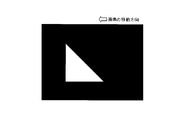
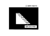
- 2A and 2B are explanatory diagrams for explaining an example of display defects.
- 2A and 2B show a display image at a certain time when a triangular object of a white image is moving in the background of a black image. It is assumed that the object has moved from the right side to the left side in the figure.
- a normal display image in which no display defect has occurred is a display image as shown in FIG. 2A.
- each pixel on the object locus changes from a white image to a black image, light leakage occurs.
- FIG. 2B the background of the black image is not normally displayed in each pixel on the locus of the object, and a tailing phenomenon occurs.
- a method of limiting the upper limit of the signal level of the video signal is known in order to suppress display defects such as the tailing phenomenon.
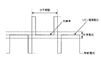
- FIG. 3A is a waveform diagram of the drive voltage when the upper limit of the signal level of the video signal is not limited
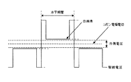
- FIG. 3B is a waveform diagram of the drive voltage when the upper limit of the signal level of the video signal is limited.
- the video signal uses a 1H inversion driving method in which the polarity is inverted every horizontal period (1H).
- the video signal shows a white image.
- the upper limit of the signal level of the video signal is not limited, as shown in FIG. 3A, a white side voltage is applied to the pixel electrode 101 as a drive voltage, which may cause a display failure. Therefore, as shown in FIG. 3B, the upper limit of the signal level of the video signal is limited so that the drive voltage does not become the white voltage. As a result, there is no change from the white side voltage to the black side voltage, and display defects are suppressed.
- Patent Document 1 describes a liquid crystal television device that can suppress a display image from becoming dark with a display defect.
- This liquid crystal television apparatus detects the average luminance of the video signal, and increases the upper limit of the signal level of the video signal when the average luminance is a predetermined threshold value or more.
- the average brightness depends on the image of the intermediate gradation between the white image and the black image, so even if the average brightness is the same, there are many white images and few black images, or there are few white images and many black images. There is.
- An object of the present invention is to provide a video display device and a video correction method that solve the above-described problem that display defects cannot be appropriately suppressed.
- a video display device supplies a liquid crystal panel, input means for receiving a video signal, and a driving voltage corresponding to the video signal received by the input means to the liquid crystal panel, and displays the video indicated by the video signal.
- the detection means for detecting the histogram representing the relationship between the signal level of the video signal received by the input means and the number of pixels, and the histogram detected by the detection means, A first ratio of pixels whose signal level with respect to the total number of pixels of the histogram is equal to or greater than a predetermined first specified value, and a signal level with respect to the total number of pixels that is less than a second specified value that is less than the first specified value.
- a calculating means for calculating a second ratio of pixels, and the driving means supplies the liquid crystal panel according to the first ratio and the second ratio calculated by the calculating means.
- a correction means for correcting the lower limit of the dynamic voltage.
- a video correction method is a video correction method by a video display device that supplies a driving voltage corresponding to a video signal to a liquid crystal panel and displays a video indicated by the video signal on the liquid crystal panel.
- a histogram representing the relationship between the signal level and the number of pixels is detected, and based on the detected histogram, the signal level for the total number of pixels of the histogram is the first number of pixels having a predetermined predetermined value or more.
- One ratio and a second ratio of pixels whose signal level with respect to the total number of pixels is equal to or smaller than the second specified value is less than the first specified value, and according to the calculated first ratio and second ratio The lower limit of the drive voltage supplied to the liquid crystal panel is corrected.
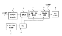
- FIG. 4 is a block diagram showing the configuration of the video display device according to the first embodiment of the present invention.
- the video display apparatus includes a video signal processing circuit 1, an amplification unit 2, a drive unit 3, a liquid crystal panel 4, a histogram detection unit 5, and a CPU 6.
- the video signal processing circuit 1 is an example of input means.
- the video signal processing circuit 1 receives a video signal.
- the video signal processing circuit 1 performs signal processing on the received video signal.
- the video signal processing circuit 1 performs gamma correction, D / A conversion, and the like as signal processing.
- the video signal after the signal processing is a DC signal.
- the amplification unit 2 is an example of a correction unit.
- the amplifying unit 2 amplifies the video signal and corrects the white level of the video signal.
- the white level is the amplitude when the video signal is brightest.
- the driving unit 3 supplies a driving voltage corresponding to the video signal whose white level has been corrected by the amplifying unit 2 to the liquid crystal panel 4 so that the video indicated by the video signal is displayed on the liquid crystal panel 4.
- the liquid crystal panel 4 is a normally white type liquid crystal panel. For this reason, the image displayed on the liquid crystal panel 4 becomes brighter as the drive voltage is smaller, and is brightest at the lower limit of the drive voltage. Therefore, the white level of the video signal corresponds to the lower limit of the drive voltage. Therefore, the amplifying unit 2 corrects the lower limit of the drive voltage by correcting the white level of the video signal.
- the drive unit 3 includes an inversion / AC drive unit 7 and a liquid crystal drive circuit 8, and each unit performs the following processing.
- the inversion / AC drive unit 7 converts the video signal whose amplitude is corrected by the amplification unit 2 into an AC signal whose polarity is inverted at a predetermined period.
- the predetermined cycle is, for example, one horizontal period or one field period.
- the liquid crystal drive circuit 8 generates a drive voltage corresponding to the video signal converted into an AC signal by the inversion / AC drive unit 7.
- the liquid crystal drive circuit 8 supplies the drive voltage to the liquid crystal panel 4 and displays the video indicated by the video signal on the liquid crystal panel 4.
- the histogram detection unit 5 is an example of a detection unit.
- the histogram detection unit 5 detects a video histogram representing the relationship between the signal level of the video signal subjected to signal processing in the video signal processing circuit 1 and the number of pixels. Note that the histogram detection unit 5 preferably detects a video histogram for each frame.
- the histogram detection unit 5 may detect a plurality of color histograms representing the signal level and the number of pixels of each of the plurality of color component signals included in the video signal as the video histogram.
- a luminance histogram representing the signal level and the number of pixels of the luminance signal included may be detected.
- CPU 6 is an example of calculation means. Based on the video histogram detected by the histogram detector 5, the CPU 6 calculates the ratio of white pixels and the ratio of black pixels to the total number of pixels in the video histogram.
- the white side pixel is a pixel whose signal level is equal to or higher than a predetermined first predetermined value.
- the black pixel is a pixel whose signal level is equal to or lower than a second predetermined value.
- the second specified value is smaller than the first specified value.
- the first specified value is, for example, a value that is 80% of the maximum signal level.
- the second specified value is, for example, a value that is 20% of the maximum signal level.
- the white pixel ratio is an example of a first ratio
- the black pixel ratio is an example of a second ratio.
- the CPU 6 determines the correction amount of the white level of the video signal by the amplifying unit 2 according to the calculated white pixel ratio and black pixel ratio.
- the correction amount indicates a ratio of the white level of the corrected video signal to the white level of the video signal before correction.
- the amplifying unit 2 corrects the white level of the video signal in accordance with the ratio of white pixels and the ratio of black pixels.
- the CPU 6 adjusts the correction amount so that the lower limit of the drive voltage becomes a predetermined value.
- the CPU 6 adjusts the correction amount so that the lower limit of the drive voltage is equal to or less than a predetermined value and becomes smaller as the ratio of the white pixels increases.
- the CPU 6 adjusts the correction amount so that the lower limit of the drive voltage is smaller as the ratio of the black pixels is smaller. Note that the lower the drive voltage, the smaller the lower limit of the drive voltage.
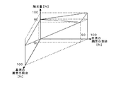
- FIG. 5 is an explanatory diagram showing the relationship between the correction amount, the ratio of black level pixels, and the ratio of white level pixels.
- the threshold is 10%
- the correction amount corresponding to the predetermined value is 80%.
- the correction amount is 100%. That is, the corrected white level is made equal to the uncorrected white level.
- the correction amount is 80% when the ratio of black pixels is 10% or less, and when the ratio of black pixels is 0% to 10%, the ratio of white pixels and black pixels Depending on the ratio, it varies between 80% and 100%.
- the CPU 6 calculates a correction amount for each color histogram based on the color histogram. When these correction amounts are different, if the respective white levels of the color component signals are corrected according to the respective correction amounts, the respective white levels of the color component signals are shifted and color shifts are generated. There is. In order to prevent this color misregistration, the CPU 6 adjusts the correction amount of the amplifying unit 2 to the smallest correction amount among those correction amounts to maximize the lower limit of the drive voltage.
- the CPU 6 responds to the blue color-specific histogram.
- the correction amount of the amplification unit 2 is adjusted.
- the CPU 6 adjusts the correction amount of the amplifying unit 2 so that the lower limit of the drive voltage becomes a predetermined value, and then the lower limit of the drive voltage is gradually reduced when the ratio of the pixels on the black side becomes zero.
- the correction amount may be adjusted. For example, the CPU 6 increases the correction amount to 100% so that the lower limit of the drive voltage becomes the minimum value “0” over several seconds.
- the CPU 6 appropriately controls the inversion / AC drive unit 7 and the liquid crystal drive circuit 8 such as on / off control of the inversion / AC drive unit 7 and the liquid crystal drive circuit 8 and setting of the drive method.
- FIG. 6 is a flowchart for explaining the operation of the video display device.
- step S101 when the video signal processing circuit 1 receives the video signal, the video signal processing circuit 1 performs various signal processing on the video signal, and outputs the video signal subjected to the signal processing to the amplification unit 2 and the histogram detection unit 5.
- the histogram detection unit 5 receives the video signal, it executes Step S102.
- step S102 the histogram detector 5 detects a video histogram based on the video signal. Whether the color histogram or the luminance histogram is detected as the video histogram may be determined in advance or may be set by the user of the video display device.
- the histogram detector 5 detects the video histogram, it outputs the video histogram to the CPU 6.
- the CPU 6 accepts the video histogram, it executes step S103.
- step S103 based on the video histogram, the CPU 6 calculates a ratio of white pixels and a ratio of black pixels to the total number of pixels of the video histogram.
- the CPU 6 obtains the white level correction amount of the video signal by the amplifying unit 2 based on the calculated white pixel ratio and black pixel ratio.
- the CPU 6 outputs the correction amount to the amplification unit 2.
- the amplification unit 2 executes step S104.
- step S104 the amplification unit 2 sets the correction amount to itself. Then, the amplification unit 2 corrects the white level of the video signal to the set correction amount. Note that it is desirable to delay the video signal using a frame memory or the like so that the white level of the frame used when obtaining the correction amount is corrected to the correction amount.
- the amplifying unit 2 When the white level of the video signal is corrected, the amplifying unit 2 outputs the video signal with the corrected white level to the inversion / AC drive unit 7.
- the inversion / AC drive unit 7 executes Step S105.
- step S105 the inversion / AC drive unit 7 converts the video signal into an AC signal whose polarity is inverted at a predetermined period, and outputs the converted video signal to the liquid crystal drive circuit 8.
- the liquid crystal driving circuit 8 receives the video signal, the liquid crystal driving circuit 8 generates a driving voltage corresponding to the video signal and supplies the driving voltage to the liquid crystal panel 4.
- the liquid crystal panel 4 is driven according to the supplied drive voltage, displays the video indicated by the video signal, and ends the operation.
- the driving unit 3 supplies a driving voltage corresponding to the video signal received by the video signal processing circuit 1 to the liquid crystal panel 4 so that the video indicated by the video signal is displayed on the liquid crystal panel 4.
- the histogram detector 5 detects a video histogram representing the relationship between the signal level of the video signal received by the video signal processing circuit 1 and the number of pixels. Based on the histogram detected by the histogram detection unit 5, the CPU 6 determines the ratio of pixels having a signal level with respect to the total number of pixels in the histogram (pixels on the white side) equal to or higher than the first specified value, and all the histograms.
- the ratio of pixels (black side pixels) whose signal level with respect to the number of pixels is less than the first specified value and less than or equal to the second specified value is calculated.
- the amplifying unit 2 corrects the lower limit of the driving voltage that the driving unit 3 supplies to the liquid crystal panel 4 in accordance with the white pixel ratio and the black pixel ratio calculated by the CPU 6.
- the lower limit of the drive voltage is corrected according to the ratio of white pixels and the ratio of black pixels. Accordingly, it is possible to appropriately determine an image in which a display defect is likely to occur, and thus it is possible to appropriately suppress the display defect.
- the amplifying unit 2 sets the lower limit of the drive voltage to a predetermined value. Further, when the ratio of the black pixels is less than the threshold, the lower limit of the drive voltage is smaller than a predetermined value, and the smaller the white pixels, the smaller the ratio.
- the display image can be brightened as the ratio of the white side pixels is increased. Therefore, it is possible to appropriately suppress display defects while suppressing the display image from becoming dark.
- the amplifying unit 2 decreases the lower limit of the drive voltage as the ratio of black pixels decreases.
- the amplifying unit 2 corrects the white level of the video signal to correct the lower limit of the drive voltage. In this case, the amplitude of the drive voltage can be easily corrected.
- the lower limit of the drive voltage is corrected by correcting the white level of the video signal.
- the lower limit of the drive voltage is reduced by superimposing the DC voltage on the drive voltage. Restrict.
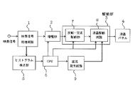
- FIG. 7 is a block diagram showing the configuration of the video display device of this embodiment.
- the video display device further includes a DC generation circuit 9 in addition to the configuration shown in FIG. 4.
- the amplification unit 2 of the present embodiment sets the white level amplitude of the video signal to a minimum value (0 V).
- the DC generation circuit 9 is an example of a correction unit.
- the direct current generation circuit 9 generates a direct current voltage that is superimposed on a drive voltage corresponding to a video signal having a signal level equal to or higher than a predetermined level, and superimposes the direct current voltage on the drive voltage generated by the liquid crystal drive circuit 8. Thereby, the lower limit of the drive voltage is corrected.
- the CPU 6 adjusts the magnitude of the DC voltage generated by the DC generation circuit 9 in accordance with the calculated white pixel ratio and black pixel ratio.
- the direct current generation circuit 9 superimposes the direct current voltage on the drive voltage corresponding to the video signal whose signal level is equal to or higher than the predetermined level according to the ratio of the white side pixel and the ratio of the black side pixel.
- the amplitude of the drive voltage is corrected.
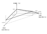
- FIG. 8 is an explanatory diagram showing the relationship between the magnitude of the DC voltage, the ratio of black level pixels, and the ratio of white level pixels. Note that the magnitude of the DC voltage is shown as a ratio to the maximum value of the amplitude of the drive voltage.
- the threshold is 10%.
- the magnitude of the DC voltage corresponding to the predetermined value is 20% of the amplitude of the drive voltage.
- the magnitude of the DC voltage is set to 0%.
- the magnitude of the DC voltage is 20% when the ratio of black pixels is 10% or less, and when the ratio of black pixels is 0% to 10%, the ratio of white pixels and black It varies between 0% and 20% depending on the ratio of the pixels on the side.
- the CPU 6 adjusts the magnitude of the DC voltage so that the lower limit of the drive voltage becomes a predetermined value, and then the lower limit of the drive voltage is gradually reduced when the ratio of the pixels on the black side becomes 0.
- the magnitude of the DC voltage may be adjusted. For example, the CPU 6 decreases the magnitude of the DC voltage to 0 so that the lower limit of the drive voltage becomes the minimum value “0” over several seconds.
- the DC generation circuit 9 corrects the amplitude of the drive voltage by superimposing the DC voltage on the drive voltage corresponding to the video signal whose signal level is a predetermined level or higher.
- the amplitude of the drive voltage can be corrected without correcting the amplitude of the video signal.
- FIG. 9 is a block diagram showing the configuration of the video image display device of the present embodiment.
- the video display apparatus has a moving image detection unit 10 instead of the histogram detection unit 5 in the configuration shown in FIG. 1.
- the moving image detection unit 10 determines whether the video indicated by the video signal processed by the video signal processing circuit 1 is a moving image or a still image.
- the moving image detecting unit 10 detects the APL or the video histogram of the frame of the video signal for each frame as the moving image determination value, and obtains the difference between the moving image determination value of the current frame and the moving image determination value of the next frame.
- the difference is larger than a predetermined value
- the video indicated by the video signal is determined as a moving image
- the difference is smaller than the value
- the video indicated by the video signal is determined as a still image.
- the moving image detection unit 10 detects the polarity and form of the synchronization signal of the video signal (separate, composite, sync-on-G, etc.), and the type of the input terminal to which the video signal is input (VIDEO / S-VIDEO input terminal, Based on the component input terminal and the HDMI input terminal, the format of the video signal may be determined to determine whether the video signal is a moving image or a still image. In this case, if the format of the video signal is a video format such as 1080p or 720p, the video detection unit 10 determines that the video indicated by the video signal is a moving image.
- the moving image detection unit 10 detects the video histogram of the video signal in the same manner as the histogram detection unit 5 in FIG.
- the CPU 6 adjusts the correction amount of the white level of the video signal by the amplification unit 2 as in the first embodiment.
- the amplification unit 2 corrects the lower limit of the drive voltage when the moving image detection unit 10 determines that the video is a moving image.
- the CPU 6 does not adjust the correction amount.
- the amplification unit 2 minimizes the amplitude of the white level of the video signal.
- the CPU 6 converts the white level of the video signal into a video histogram (a white pixel ratio and a black pixel ratio).
- the correction amount may be adjusted so as to be a constant value that does not depend. This is because, as a human visual characteristic, a moving image is harder to detect brightness than a still image, and thus it is difficult for a human to detect it even if the screen is darkened.
- the histogram detection unit 5 of the first embodiment is replaced with the moving image detection unit 10
- the histogram detection unit 5 of the second embodiment may be replaced with the moving image detection unit 10.
- the moving image detection unit 10 determines whether the video indicated by the video signal is a moving image or a still image.
- the amplification unit 2 corrects the lower limit of the drive voltage.
Landscapes
- Engineering & Computer Science (AREA)
- Chemical & Material Sciences (AREA)
- Crystallography & Structural Chemistry (AREA)
- Physics & Mathematics (AREA)
- Computer Hardware Design (AREA)
- General Physics & Mathematics (AREA)
- Theoretical Computer Science (AREA)
- Control Of Indicators Other Than Cathode Ray Tubes (AREA)
- Liquid Crystal Display Device Control (AREA)
- Liquid Crystal (AREA)
- Transforming Electric Information Into Light Information (AREA)
Abstract
Priority Applications (4)
| Application Number | Priority Date | Filing Date | Title |
|---|---|---|---|
| JP2011505766A JP5187789B2 (ja) | 2009-03-27 | 2009-03-27 | 映像表示装置および映像補正方法 |
| US13/260,301 US9024935B2 (en) | 2009-03-27 | 2009-03-27 | Image display apparatus and image correction method |
| CN200980158395.5A CN102365674B (zh) | 2009-03-27 | 2009-03-27 | 图像显示设备和图像校正方法 |
| PCT/JP2009/056220 WO2010109643A1 (fr) | 2009-03-27 | 2009-03-27 | Procédé d'affichage et de correction d'images |
Applications Claiming Priority (1)
| Application Number | Priority Date | Filing Date | Title |
|---|---|---|---|
| PCT/JP2009/056220 WO2010109643A1 (fr) | 2009-03-27 | 2009-03-27 | Procédé d'affichage et de correction d'images |
Publications (1)
| Publication Number | Publication Date |
|---|---|
| WO2010109643A1 true WO2010109643A1 (fr) | 2010-09-30 |
Family
ID=42780352
Family Applications (1)
| Application Number | Title | Priority Date | Filing Date |
|---|---|---|---|
| PCT/JP2009/056220 Ceased WO2010109643A1 (fr) | 2009-03-27 | 2009-03-27 | Procédé d'affichage et de correction d'images |
Country Status (4)
| Country | Link |
|---|---|
| US (1) | US9024935B2 (fr) |
| JP (1) | JP5187789B2 (fr) |
| CN (1) | CN102365674B (fr) |
| WO (1) | WO2010109643A1 (fr) |
Cited By (2)
| Publication number | Priority date | Publication date | Assignee | Title |
|---|---|---|---|---|
| JP2015075770A (ja) * | 2013-10-11 | 2015-04-20 | 三星電子株式会社Samsung Electronics Co.,Ltd. | 映像処理装置、映像処理装置を含む電子装置、及び、映像処理方法 |
| JP2016118606A (ja) * | 2014-12-19 | 2016-06-30 | キヤノン株式会社 | 映像信号生成装置、液晶表示装置、映像信号生成方法および映像信号生成プログラム |
Families Citing this family (3)
| Publication number | Priority date | Publication date | Assignee | Title |
|---|---|---|---|---|
| CN103021345B (zh) * | 2012-12-18 | 2014-12-24 | 四川长虹电器股份有限公司 | 一种消除液晶屏漏光的方法 |
| WO2015186212A1 (fr) * | 2014-06-04 | 2015-12-10 | 堺ディスプレイプロダクト株式会社 | Dispositif d'affichage à cristaux liquides et procédé d'affichage |
| KR102507208B1 (ko) * | 2018-01-10 | 2023-03-07 | 삼성디스플레이 주식회사 | 유기 발광 표시 장치 및 그 구동방법 |
Citations (3)
| Publication number | Priority date | Publication date | Assignee | Title |
|---|---|---|---|---|
| JPH06332399A (ja) * | 1993-05-19 | 1994-12-02 | Fujitsu General Ltd | 電子ディスプレイの制御方法およびその装置 |
| JP2007164208A (ja) * | 2001-04-25 | 2007-06-28 | Matsushita Electric Ind Co Ltd | 映像表示装置 |
| JP2008020887A (ja) * | 2006-06-15 | 2008-01-31 | Victor Co Of Japan Ltd | 映像表示装置及び映像表示方法 |
Family Cites Families (10)
| Publication number | Priority date | Publication date | Assignee | Title |
|---|---|---|---|---|
| US5731796A (en) * | 1992-10-15 | 1998-03-24 | Hitachi, Ltd. | Liquid crystal display driving method/driving circuit capable of being driven with equal voltages |
| JP3902390B2 (ja) | 2000-09-29 | 2007-04-04 | 三洋電機株式会社 | 映像信号処理回路 |
| EP1383104B1 (fr) | 2001-04-25 | 2011-05-04 | Panasonic Corporation | Appareil et procede d'affichage video |
| JP4137404B2 (ja) | 2001-05-10 | 2008-08-20 | シャープ株式会社 | 液晶表示装置および液晶表示装置における画像表示方法 |
| JP4453805B2 (ja) | 2003-03-25 | 2010-04-21 | セイコーエプソン株式会社 | 画像処理システム、プロジェクタ、プログラム、情報記憶媒体および画像処理方法 |
| JP3975357B2 (ja) | 2003-06-12 | 2007-09-12 | 船井電機株式会社 | 液晶テレビジョン装置 |
| JP4819404B2 (ja) | 2005-06-07 | 2011-11-24 | シャープ株式会社 | 液晶表示装置 |
| JP2007133051A (ja) | 2005-11-09 | 2007-05-31 | Hitachi Displays Ltd | 画像表示装置 |
| WO2007125628A1 (fr) * | 2006-04-28 | 2007-11-08 | Sharp Kabushiki Kaisha | Écran à cristaux liquides, son pp de commande et dispositif électronique |
| CN100524446C (zh) | 2006-06-15 | 2009-08-05 | 日本胜利株式会社 | 影像显示装置及影像显示方法 |
-
2009
- 2009-03-27 WO PCT/JP2009/056220 patent/WO2010109643A1/fr not_active Ceased
- 2009-03-27 CN CN200980158395.5A patent/CN102365674B/zh not_active Expired - Fee Related
- 2009-03-27 JP JP2011505766A patent/JP5187789B2/ja not_active Expired - Fee Related
- 2009-03-27 US US13/260,301 patent/US9024935B2/en active Active
Patent Citations (3)
| Publication number | Priority date | Publication date | Assignee | Title |
|---|---|---|---|---|
| JPH06332399A (ja) * | 1993-05-19 | 1994-12-02 | Fujitsu General Ltd | 電子ディスプレイの制御方法およびその装置 |
| JP2007164208A (ja) * | 2001-04-25 | 2007-06-28 | Matsushita Electric Ind Co Ltd | 映像表示装置 |
| JP2008020887A (ja) * | 2006-06-15 | 2008-01-31 | Victor Co Of Japan Ltd | 映像表示装置及び映像表示方法 |
Cited By (2)
| Publication number | Priority date | Publication date | Assignee | Title |
|---|---|---|---|---|
| JP2015075770A (ja) * | 2013-10-11 | 2015-04-20 | 三星電子株式会社Samsung Electronics Co.,Ltd. | 映像処理装置、映像処理装置を含む電子装置、及び、映像処理方法 |
| JP2016118606A (ja) * | 2014-12-19 | 2016-06-30 | キヤノン株式会社 | 映像信号生成装置、液晶表示装置、映像信号生成方法および映像信号生成プログラム |
Also Published As
| Publication number | Publication date |
|---|---|
| CN102365674B (zh) | 2014-08-20 |
| US20120019507A1 (en) | 2012-01-26 |
| JPWO2010109643A1 (ja) | 2012-09-27 |
| JP5187789B2 (ja) | 2013-04-24 |
| US9024935B2 (en) | 2015-05-05 |
| CN102365674A (zh) | 2012-02-29 |
Similar Documents
| Publication | Publication Date | Title |
|---|---|---|
| JP5187789B2 (ja) | 映像表示装置および映像補正方法 | |
| JP2010008739A (ja) | 映像信号制御装置、映像表示システム、及び映像信号制御方法 | |
| JP5131509B2 (ja) | 画像表示装置、該画像表示装置に用いられる駆動回路及び駆動方法 | |
| CN103069478A (zh) | 视频显示控制装置 | |
| JP2007155840A5 (fr) | ||
| KR100887679B1 (ko) | 액정 이미저에서 스파클 결함을 감소시키는 방법 | |
| KR101665132B1 (ko) | 영상표시기기의 화질 개선 장치 및 방법 | |
| JP5392856B2 (ja) | 映像表示装置、映像信号処理方法、およびプログラム | |
| JP5679356B2 (ja) | 補正方法及び表示装置 | |
| CN104106109B (zh) | 视频显示控制装置 | |
| JP4137404B2 (ja) | 液晶表示装置および液晶表示装置における画像表示方法 | |
| CN103000154A (zh) | 一种液晶面板的驱动方法、装置及显示装置 | |
| JP2014090266A (ja) | 画像表示装置およびその制御方法 | |
| US20120026185A1 (en) | Display apparatus and display method | |
| JP4819404B2 (ja) | 液晶表示装置 | |
| KR100469282B1 (ko) | 자동 잔상 방지 기능을 갖는 디스플레이 기기 및 그 잔상방지 방법 | |
| WO2015166531A1 (fr) | Dispositif d'affichage | |
| JP2010128040A (ja) | 表示装置 | |
| JP2006295845A (ja) | 映像信号処理回路 | |
| KR101539616B1 (ko) | 화질 개선 방법 및 그 장치 | |
| KR100784690B1 (ko) | 자동 샤프니스 제어 방법 | |
| WO2012147602A1 (fr) | Appareil d'affichage à cristaux liquides | |
| KR20160082889A (ko) | 데이터 변환장치와 이를 포함하는 표시장치 | |
| JP2011112726A (ja) | 画像表示装置およびテレビジョン | |
| JP2009134186A (ja) | 画像信号処理装置 |
Legal Events
| Date | Code | Title | Description |
|---|---|---|---|
| WWE | Wipo information: entry into national phase |
Ref document number: 200980158395.5 Country of ref document: CN |
|
| 121 | Ep: the epo has been informed by wipo that ep was designated in this application |
Ref document number: 09842257 Country of ref document: EP Kind code of ref document: A1 |
|
| WWE | Wipo information: entry into national phase |
Ref document number: 2011505766 Country of ref document: JP |
|
| WWE | Wipo information: entry into national phase |
Ref document number: 13260301 Country of ref document: US |
|
| NENP | Non-entry into the national phase |
Ref country code: DE |
|
| 122 | Ep: pct application non-entry in european phase |
Ref document number: 09842257 Country of ref document: EP Kind code of ref document: A1 |