WO2010109856A1 - 表示パネル点灯検査装置、及び表示パネル点灯検査方法 - Google Patents
表示パネル点灯検査装置、及び表示パネル点灯検査方法 Download PDFInfo
- Publication number
- WO2010109856A1 WO2010109856A1 PCT/JP2010/002075 JP2010002075W WO2010109856A1 WO 2010109856 A1 WO2010109856 A1 WO 2010109856A1 JP 2010002075 W JP2010002075 W JP 2010002075W WO 2010109856 A1 WO2010109856 A1 WO 2010109856A1
- Authority
- WO
- WIPO (PCT)
- Prior art keywords
- defect
- display panel
- line
- defects
- inspection
- Prior art date
- Legal status (The legal status is an assumption and is not a legal conclusion. Google has not performed a legal analysis and makes no representation as to the accuracy of the status listed.)
- Ceased
Links
Images



Classifications
-
- G—PHYSICS
- G09—EDUCATION; CRYPTOGRAPHY; DISPLAY; ADVERTISING; SEALS
- G09G—ARRANGEMENTS OR CIRCUITS FOR CONTROL OF INDICATING DEVICES USING STATIC MEANS TO PRESENT VARIABLE INFORMATION
- G09G3/00—Control arrangements or circuits, of interest only in connection with visual indicators other than cathode-ray tubes
- G09G3/006—Electronic inspection or testing of displays and display drivers, e.g. of LED or LCD displays
-
- G—PHYSICS
- G02—OPTICS
- G02F—OPTICAL DEVICES OR ARRANGEMENTS FOR THE CONTROL OF LIGHT BY MODIFICATION OF THE OPTICAL PROPERTIES OF THE MEDIA OF THE ELEMENTS INVOLVED THEREIN; NON-LINEAR OPTICS; FREQUENCY-CHANGING OF LIGHT; OPTICAL LOGIC ELEMENTS; OPTICAL ANALOGUE/DIGITAL CONVERTERS
- G02F1/00—Devices or arrangements for the control of the intensity, colour, phase, polarisation or direction of light arriving from an independent light source, e.g. switching, gating or modulating; Non-linear optics
- G02F1/01—Devices or arrangements for the control of the intensity, colour, phase, polarisation or direction of light arriving from an independent light source, e.g. switching, gating or modulating; Non-linear optics for the control of the intensity, phase, polarisation or colour
- G02F1/13—Devices or arrangements for the control of the intensity, colour, phase, polarisation or direction of light arriving from an independent light source, e.g. switching, gating or modulating; Non-linear optics for the control of the intensity, phase, polarisation or colour based on liquid crystals, e.g. single liquid crystal display cells
- G02F1/1306—Details
- G02F1/1309—Repairing; Testing
Definitions
- the present invention relates to a display panel lighting inspection apparatus for applying a driving signal to a matrix driving type display panel represented by a liquid crystal panel, an EL panel or the like to turn it on and inspecting a defect state of the display panel.
- a flat panel display such as a liquid crystal panel has been visually inspected for minute point defects, foreign object defects, spots, unevenness, etc. in a display device in order to ensure quality. Yes.
- FPD flat panel display
- a drive signal is given to the display panel to be inspected to turn it on, an area sensor is used to image the display screen of the display panel to be inspected, and the inspection is automated by image processing. Yes.
- it is required to measure the strength of the defect by image processing, and to determine a defect that is equal to or higher than a preset detection threshold as a defect, and the impression when the visual inspector looks at the display panel to be inspected Therefore, it was necessary to be a judgment approximate to the judgment.
- Patent Document 1 describes a method for quantitatively evaluating the image quality of an inspection screen as a response to the above request.
- the defect to be detected includes a line defect that appears in the horizontal direction or the vertical direction of the display panel to be inspected.
- An image including the line defect is captured by an area sensor, and the captured image is captured by a predetermined algorithm.
- line defects are automatically detected.
- factors such as length, thickness, and contrast are comprehensively determined to determine whether the display panel to be inspected is good or bad, and further, to determine ranks such as A to D Is done.
- Patent Document 2 describes a display panel inspection method in which an index capable of quantitatively evaluating defects is introduced.
- the inspector's visual judgment depends on the sensuality and skill of each individual, and thus tends to vary, but in order to avoid this, the image is captured by an area sensor, and the captured image is converted into a specific algorithm.
- the image quality index For example, the captured image is subjected to differential processing, and the total sum is obtained by multiplying the area of the region having the same differential value as the image quality index.
- the display panel is evaluated according to this index.
- Japanese Patent Publication Japanese Patent Laid-Open No. 2006-250876 (published on September 21, 2006)” Japanese Patent Publication “Japanese Laid-Open Patent Publication No. 2000-215310 (Released on August 4, 2000)”
- Some display panels in which defects are detected by automatic inspection can be repaired in the repair process depending on the type of defect.
- the factory production management system (CIM) and the conveyance line use the determination by automatic inspection or the detailed inspection result to direct the inspected display panel to each repair process. For example, in the laser repair process, an operator uses the result of the automatic inspection to move the microscope field of view to the defective pixel, cut the wiring causing the defect while checking the defective pixel, Modify to pixel.
- Patent Document 1 and Patent Document 2 which are prior art documents, it is possible to stably perform judgments and sensory judgments that approximate the judgment of a visual inspector, but can the defect be repaired? It cannot be determined and output, and even if repair is possible, the repaired part cannot be specified and output. Further, since it is impossible to determine what kind of defect it is, the display panel that needs to be repaired cannot be directed to an optimal repair process. Further, since the position of the portion to be repaired is not clear, for example, it takes time to move the microscope visual field position to repair the line defect.
- the present invention has been made in view of the above-described problems of the prior art, and can detect a defect in a display panel, and can classify the display panel to be inspected in which the defect is found for each type of defect. And it aims at providing the display panel inspection apparatus which can also output the positional information on the said defect.
- a signal generator for driving a display panel to be lit in one or more display modes and a display image of the display panel driven to be lit are displayed.
- An image pickup apparatus that picks up an image, an inspection processing unit that obtains data relating to defects by inspecting and analyzing a lighting screen of a display panel imaged by the image pickup device, and the display panel using data relating to defects from the inspection processing unit
- a display panel lighting inspection apparatus including a defect classification processing unit that classifies defects according to defect types, wherein the defect classification processing unit is obtained from the defect classification table prepared in advance and the inspection processing unit. It is characterized in that the defect is classified by type in comparison with the data related to the defect, and the type of defect and the position of the defect are output.
- the type and position of the defect of the display panel can be easily known, and in the case of a defect that can be repaired, the display panel can be sent to a repair process optimal for the repair.
- the display panel to be inspected is driven to be lit in one or more display modes, and the display of the display panel that is lit is displayed.
- a display panel lighting inspection method for detecting a defect type and a defect position of a display panel from an image, obtained by the image acquisition step for acquiring a display image of the display panel driven to be lit, and the image acquisition step The inspection step for inspecting and analyzing the displayed image to acquire data on defects, comparing the defect classification table prepared in advance with the data on defects obtained in the inspection step, and classifying the defects by type And outputting a defect type and a defect position.
- the signal generator for driving the display panel to be lit in one or more display modes, and the imaging for capturing the display image of the display panel driven to be lit.
- An inspection processing section for inspecting and analyzing a lighting screen of the display panel imaged by the imaging apparatus, obtaining data relating to the defect, and detecting defects in the display panel using data relating to the defect from the inspection processing section.
- a display panel lighting inspection apparatus including a defect classification processing unit that classifies by defect type, wherein the defect classification processing unit includes a defect classification table prepared in advance and data relating to the defects obtained from the inspection processing unit Are characterized in that defects are classified by type, and the type of defect and the position of the defect are output.
- the display panel to be inspected is driven to be lit in one or more types of display modes, and the type of display panel defect is determined from the display image of the lighting-driven display panel.
- a display panel lighting inspection method for detecting a position of a defect wherein an image acquisition step for acquiring a display image of the lighting-driven display panel, and an inspection and analysis of the display image obtained by the image acquisition step are performed.
- the inspection step for acquiring data relating to defects, the defect classification table prepared in advance, and the data relating to the defects obtained in the inspection step are compared, the defects are classified by type, and the type of defect and the position of the defect are determined. And a step of outputting.
- FIG. 1 is a diagram showing an embodiment of the present invention, and schematically shows an overall configuration of a display panel lighting inspection apparatus when a liquid crystal panel is set as a display panel to be inspected.
- the lighting inspection device includes an area sensor 1 (imaging device) for taking an image displayed on the liquid crystal panel 4 to be inspected, a main control unit 6 (control unit) that controls the entire lighting inspection device, and a liquid crystal panel to be inspected.
- an area sensor mount and an area sensor attitude adjustment jig (not shown), a factory production management system (CIM) connected to the main control unit 6, and a target controlled by the factory production management system (CIM).
- a transport line for transporting the inspection liquid crystal panel and the like are included.
- the CIM is generally connected to the main control unit 6 through a LAN (local area network), and further connected to each device control computer in the process.
- the display panel lighting inspection device When the display panel to be inspected is the liquid crystal panel 4, the display panel lighting inspection device further includes a backlight 2, a back polarizing plate 3, and a front polarizing plate 5.
- the liquid crystal panel 4 to be inspected is set at a position sandwiched between the back polarizing plate 3 and the front polarizing plate 5.
- the outline of the inspection process of the liquid crystal panel 4 using the display panel inspection apparatus described above is as follows.
- the liquid crystal panel 4 in a state in which the liquid crystal is sealed is transported to an inspection station by a transport line (not shown), positioned at the position shown in FIG. 1, and further contacted with the signal generator 8 necessary for lighting driving. Is taken.
- An ID for individually identifying the liquid crystal panel 4 is given to the liquid crystal panel 4 to be inspected, and various information regarding the specific liquid crystal panel 4 corresponding to each ID, for example, on the CIM side, for example Information such as panel size and inspection recipe is held.
- the inspection recipe is information indicating what kind of inspection is performed on the liquid crystal panel 4 specified by the ID, and the main control unit 6 transmits a signal according to the inspection recipe obtained from the CIM.
- the generator 8, the backlight 2, and the area sensor 1 are controlled to image the specific display area or the entire area of the liquid crystal panel 4 to be inspected. Basically, the entire screen area is imaged and the entire screen area is inspected. Further, after inspecting the entire area of the screen (rough inspection), a specific area having a defect may be imaged and inspected under optical conditions with high resolution. At this time, a plurality of lighting screens are imaged in order to inspect a number of defects. Details will be described later.
- the inspection processing unit 7 After acquiring the inspection recipe and the captured image taken by the area sensor 1, the inspection processing described in detail later is performed, and the result is output to the CIM.
- the output from the inspection processing unit 7 to the CIM includes at least the type of defect and the position of the defect.
- the output from the inspection processing unit 7 is received, and the inspection result for the liquid crystal panel 4 having the specific ID is stored and held. If there is a defect that can be repaired in the inspected liquid crystal panel 4 with the specific ID, the inspected liquid crystal panel 4 is sent to a repair process that can repair the defect according to the type of the defect. It will be.
- the CIM side has information on the type and position of the defect of the liquid crystal panel 4 to be inspected, and for example, determination of the visual field position of the microscope for correcting the line defect is performed in a very short time. Is possible.
- FIG. 2 is a diagram showing an example of a display state when the liquid crystal panel 4 is lit and displayed with a specific drive signal, and the area sensor 1 images such a display screen.
- the display gradation of the liquid crystal panel 4 to be inspected is 8 bits
- (a) in FIG. 2 represents the case where the intermediate gradation is displayed (halftone screen display mode).
- (B) shows a state of “0”, that is, a mode for displaying a black screen (black screen display mode).
- FIG. 2C shows a case where only the R pixel is displayed (R screen display mode).
- the specific position of the liquid crystal panel 4 to be inspected is indicated by the x direction (horizontal direction) and the y direction (vertical direction) as shown in the drawing with the upper left corner of the display area as the origin, and the number of picture elements is 1920 (RGB) ⁇ 1080. In this case, (0, 0)-(5759, 1079) is obtained.
- the defect indicates that there is a line defect in both the horizontal direction and the vertical direction.
- the source emission line 23 is brighter than the surrounding pixels
- 24 shows a case where there are a source black line 21 and a gate black line 22 which are darker than the surrounding pixels.
- the source emission line 23 that appeared in FIG. 2 (a) in the halftone screen display mode has disappeared.
- the display mode may be changed. This indicates that the specific bright line may not be displayed in this way by changing.
- the gate black line 22 does not appear in FIG. 2C in the R screen display mode, this also indicates that such a situation can occur depending on the type of defect.
- FIG. 3 is a flow chart showing an example of a line defect inspection procedure in the display panel lighting inspection apparatus according to the present invention.
- Each process (S1 to S8) described below is performed by the main control unit 6 of the display panel lighting inspection apparatus according to the present invention and the inspection processing unit 7 based on an instruction from the main control unit 6. However, in the following description, this point may be omitted.
- the main control unit 6 of the display panel lighting inspection apparatus starts with the panel ID, the substrate size, and the pixel size from the CIM.
- a dot is defined as one picture element), model information in which the number of pixels in the display area, the type of pixel, and the like are set, and an inspection recipe are acquired.
- the inspection recipe may be held in the inspection processing unit in advance, and the corresponding inspection recipe may be selected and read according to the panel ID. This processing is performed by the inspection processing unit 7 based on a command from the main control unit 6.
- the inspection recipe includes imaging information including lighting screen switching data, backlight output setting values, exposure time, gain setting, various setting values and detection thresholds for defect detection, a defect classification table described later, and the like.
- the main control unit 6 acquires an image captured according to the inspection recipe. That is, based on imaging information such as lighting screen switching data, at least one type of lighting screen image captured by the area sensor 1 is acquired.
- a line defect is detected using all images acquired in the image acquisition process. This processing is performed by the inspection processing unit 7 based on a command from the main control unit 6.
- Specific detection processing includes, for example, detection processing described below with reference to FIG. 4, but the present invention is not limited to the detection processing described below.
- the display area is divided so that the vertical direction has a constant size, and the vertical direction is divided into the divided areas. Is calculated (see (b) of FIG. 4).
- a portion exceeding the detection threshold a is defined as a defective portion.
- This processing is performed on the entire display portion of the liquid crystal panel to be inspected, and a line defect is detected by making a continuous defect portion one line defect as shown in FIG.
- a line defect is detected by making a continuous defect portion one line defect as shown in FIG.
- the line defect area at this time is the rectangular portion shown in FIG. 4C, and information representing the rectangular portion includes, for example, the upper left coordinates and lower right coordinates of the rectangle.
- the division of the area A, the area B, and the like is 10 equally in the vertical direction (in this case, 108 pixels) or Although it is about 20 equal parts, it is not limited to this value. If the break is narrowed, the position of the line segment can be obtained more accurately, but the calculation processing for that becomes heavy.
- disconnection position detection process S5 it is determined whether or not each of the line defects integrated by the above-described line defect integration process is caused by the disconnection. Detect position. If any one of the line defects is broken, it is determined that the integrated line defect has a break. This processing is performed by the inspection processing unit 7 based on a command from the main control unit 6. Note that the inspection processing unit 7 may perform the processing without being based on a command from the main control unit 6.
- the present invention it is detected whether or not the “line defect” detected as the line defect in the line defect detection process of S3 is a line defect based on the disconnection in the disconnection position detection process of S5.
- the disconnection position is detected.
- a vertical line defect or a horizontal direction is referred to with reference to the rectangular size shown in FIG. It is distinguished whether the line defect. That is, when the rectangle is a rectangle that is long in the vertical direction, it is determined as a line defect in the vertical direction, and when the rectangle is a rectangle that is long in the horizontal direction, it is determined as a line defect in the horizontal direction. Further, the line defects whose directions are determined are sequentially compared with all the line defects having different directions, and their intersection positions are detected.
- the comparison of the line defects may be limited to only the line defects detected in the lighting screen of the same mode, for example, the R screen display mode shown in FIG. 2C, or the line defects detected in a plurality of display modes. You may compare each other. Moreover, when there are a plurality of intersections as a result of the line defect comparison, all the intersections may be registered. Registering a plurality of intersection points is effective when the inspection apparatus cannot completely classify a plurality of line defects. For example, there are type A as the source line, type B and type C as the gate line, an intersection exists between A and B, an intersection exists between A and C, and defects in A and B due to panel characteristics In this case, it is assumed that a leak occurs at the intersection.
- intersection position detection process is effective because some line defects are caused by a leak between the source bus line (vertical direction) and the gate bus line (vertical direction). This is because the leak location is the intersection coordinate portion. That is, there is a high possibility that a leak occurs between the source bus line and the gate bus line at the intersection of the line defects, and detecting this intersection leads to finding the leak. In addition, since this leak can be repaired in a later repair process, this information is extremely useful information.
- the lighting screen information, the disconnection information, and the intersection information are added to the line defect data.
- defect classification is performed based on the line defect data obtained by the process in each step described above and the defect classification table input as the inspection recipe.
- the structure of the line defect data will be described with reference to FIG. 6, and then the defect classification will be described with a specific example with reference to FIG.
- FIG. 7 is an example of a defect classification table.
- FIG. 6 shows an example of the structure of line defect data for a single liquid crystal panel to be inspected.
- This figure shows information about line defects actually detected from the liquid crystal panel and subjected to integration, disconnection detection, and intersection detection.
- the column “lit screen” information indicating the presence / absence of a defect and the type of defect (bright line or black line) is described.
- the line defect data is composed of defect direction (vertical direction, horizontal direction), disconnection position, intersection position, and presence / absence of detection information on the lighting screen in each display mode for each line defect. That is, for example, the screen 1 is a lighting screen in the halftone screen display mode shown in FIG. 2A, and the screen 2 is a lighting screen in the black screen display mode shown in FIG.
- screen 3, screen 4, and screen 5 are a lighting screen in the R screen display mode, a lighting screen in the G screen display mode, and a lighting screen in the B screen display mode, respectively.
- the disconnection position and the intersection position may be indicated by either image coordinates or panel coordinates. In FIG. 6, only one place for entering the intersection position is provided, but the present invention is not limited to this, and a plurality of intersection positions may be entered.
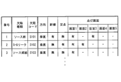
- FIG. 7 is an example of a defect classification table as described above, and includes a defect type, a defect code, a direction of a line defect, a determination result of whether there is a disconnection, a determination result of whether there is an intersection, and each display mode. It consists of presence or absence of detection information on the lighting screen.
- the conditions for determining the type of defect shown in FIG. 7, that is, the relationship between the specific defect and the lighting screen at that time can be determined based on previous experience in repair work. It can also be determined by preparing a liquid crystal panel having various defects, driving the liquid crystal panel in various display modes, and analyzing the lighting screen at that time.
- the matching process is performed from the first in the defect classification table. Is granted. If there is a matching defect type in this process, the classification of the line defect data is terminated, and the next line defect data matching process is started. If a matching defect type does not exist even after performing the matching process to the end of the defect classification table, the defect type and the defect code are not assigned.
- the inspection result includes information on the type of line defect and the position of the defect. Therefore, on the CIM side, based on the received information, a liquid crystal panel having a repairable defect can be sent to an optimal repair process for repair. In the repair process, it is possible to move the microscope field of view immediately after receiving the position information of the defect, and extremely efficient repair work is possible.
- FIG. 8 is a diagram for explaining an example of a method for obtaining the type and position of disconnection in the display panel lighting inspection apparatus according to the present invention.
- the line defect shown in FIGS. 5A and 5B will be described as an example.
- the line defect shown in FIGS. 5A and 5B are line defects in the vertical direction
- the line defect is compared with a normal position separated by a certain distance in the horizontal direction, and a contrast value with the position is calculated.
- a contrast value with the position is calculated.
- Yxy indicates the coordinate position of the target pixel
- Y (x ⁇ a) y and Y (x + a) y indicate the coordinate positions of the pixels separated by a certain distance a in the horizontal direction.
- Average (*) indicates a function for obtaining an average value.
- FIG. 8A and 5B when there is a line defect in the vertical direction, the calculation is performed over a predetermined pixel size in the horizontal direction including the line defect portion, and the results are integrated to obtain FIG. (A) and (b) are obtained.
- the vertical axis represents the magnitude of contrast
- the horizontal axis represents the position in the vertical direction on the display screen.
- 8A and 8B corresponds to the upper end of the display screen, and the right end corresponds to the lower end of the display screen.
- FIG. 8A shows a state in which the vertical line defect is based on disconnection
- FIG. 8B shows that the vertical line defect is disconnected. The state showing that it is not based is shown.
- the profiles shown in FIGS. 8A and 8B are compared with normal positions separated by a certain distance in the vertical direction, and the difference between them is calculated.
- the profiles shown in FIGS. 8C and 8D are obtained. Is obtained.
- the vertical axis represents the magnitude of the difference
- the horizontal axis represents the vertical position on the display screen as in FIGS. 8A and 8B. ing.
- FIG. 8C shows a state in which the vertical line defect is “disconnected”, and FIG. 8D shows that the vertical line defect is “not disconnected”. This is a state that shows that. If there is a change greater than or equal to the threshold value (or less) in the finally obtained profile, it is regarded as a disconnection and the coordinate position is registered as a disconnection position.
- a threshold is provided for the magnitude of the profile change in FIGS. 8A and 8C, and when the change is larger than the threshold, it is determined as “disconnected”. Further, the position where the change occurs (position in the vertical direction) is determined as the position of the disconnection.
- the horizontal position is known from the beginning. In the case of a horizontal line defect, conversely, the vertical position is known from the beginning.
- the present invention is not limited to the line defect but can be applied to other defects.
- the defect classification table described in FIG. 7 can be created based on the experience of repairing various defects so far, but a display panel having a specific defect is prepared in advance, and the display is made. It can also be created by lighting the panel in various display modes and analyzing the display screen at that time.
- the present invention can be applied to point defects.
- the disconnection of a defect classification table and the information of an intersection are unnecessary. Instead, it integrates the detection status for each lighting screen and further classifies the point defect.
- the display panel to be inspected is driven to light in the same display mode as when the defect classification table was created (corresponding to S1 in FIG. 3), and the display image at that time is displayed by the area sensor 1.
- An image is taken (corresponding to S2 in FIG. 3), and the type, position, etc. of the defect are determined using all the acquired images. That is, the type of defect and the position of the defect are determined by comparing the status of all acquired images with a defect classification table prepared in advance (corresponding to S7). In this case, if it is difficult to analyze the image itself captured by the area sensor, the obtained captured image can be subjected to processing such as differentiation.
- the present invention is not limited to the inspection of liquid crystal panels, but can also be used for inspection of EL panels, plasma panels, and the like.
- the signal generator for driving the display panel to be lit in one or more display modes, and the imaging device for capturing the display image of the lighting-driven display panel.
- an inspection processing unit for inspecting and analyzing a lighting screen of the display panel imaged by the imaging device to obtain data on the defect, and a defect on the display panel using the data on the defect from the inspection processing unit.
- Display panel lighting inspection device comprising a defect classification processing unit for classifying by type, wherein the defect classification processing unit includes a defect classification table prepared in advance and data relating to the defect obtained from the inspection processing unit; The defect is classified by type, and the type of defect and the position of the defect are output.
- the type and position of the defect of the display panel can be easily known, and in the case of a defect that can be repaired, the display panel can be sent to a repair process optimal for the repair.
- the model information and the inspection recipe of the display panel to be inspected are received, and the display panel to be inspected corresponds to the model of the display panel and the inspection recipe. It is characterized by having a control unit that automatically performs inspection.
- the defect is a line defect
- the inspection processing unit detects a line defect in each lighting screen from at least one type of captured image of the lighting screen.
- a line defect detection unit to detect, a line defect integration unit that integrates the plurality of detected line defects into one line defect, and detects whether each of the integrated line defects is a defect due to disconnection,
- a disconnection position detection unit for detecting a disconnection position on the display panel in the case of a disconnection, and an intersection position detection unit for detecting an intersection position of the horizontal and vertical line defects for each of the integrated line defects; It is characterized by having.
- the line defect integration unit that integrates the plurality of line defects into one line defect has at least a line defect detected on one or more types of lighting screens.
- the display panel is a liquid crystal panel.
- the display panel to be inspected is driven to be lit in one or more types of display modes, and the display panel display image of the display panel that has been lit is used to determine the type of defect and the defect
- Display panel lighting inspection method for detecting the position of the display panel an image acquisition step of acquiring a display image of the lighting-driven display panel, and a display image obtained by the image acquisition step is inspected and analyzed
- the inspection step for acquiring data, the defect classification table prepared in advance, and the data related to the defect obtained in the inspection step are compared, the defect is classified by type, and the type of defect and the position of the defect are output. And a step.
- the defect of the display panel is a line defect
- the inspection step detects a line defect of the display image acquired in the image acquisition step.
- it has a break position detection step for detecting a break position, and an intersection position detection step for detecting the intersection position of the line defect in the horizontal direction and the vertical direction for each of the integrated line defects. Yes.
Landscapes
- Physics & Mathematics (AREA)
- Nonlinear Science (AREA)
- General Physics & Mathematics (AREA)
- Engineering & Computer Science (AREA)
- Liquid Crystal (AREA)
- Chemical & Material Sciences (AREA)
- Crystallography & Structural Chemistry (AREA)
- Optics & Photonics (AREA)
- Computer Hardware Design (AREA)
- Theoretical Computer Science (AREA)
- Testing Of Optical Devices Or Fibers (AREA)
- Devices For Indicating Variable Information By Combining Individual Elements (AREA)
Abstract
本発明に係る表示パネル点灯検査装置は、検査対象の表示パネル(4)を駆動する信号発生部(8)と、該信号発生部(8)からの信号によって駆動された表示パネル(4)の表示画像を撮像するエリアセンサ(1)と、エリアセンサ(1)からの画像を検査および分析して欠陥の種別と欠陥位置を決定する検査処理部(7)と、検査装置全体の制御をつかさどる主制御部(6)とを有する。本発明に係る表示パネル点灯検査装置によれば、表示パネルの欠陥の有無を検査して、欠陥があった場合、欠陥の種別と欠陥の場所を判定できる。
Description
本発明は、液晶パネル、ELパネル等に代表されるマトリックス駆動型の表示パネルに対して駆動信号を与えて点灯状態にし、該表示パネルの欠陥状況を検査するための表示パネル点灯検査装置に関する。
ハイビジョン放送の開始および普及に併せ、高品質な画像表示装置を備えたテレビが広く普及している。この高品質な画像表示装置には、液晶パネルに代表される大画面、高精細、薄型の所謂フラットパネルディスプレイ(FPD)が用いられているが、表示画面中に輝点等の欠陥があると著しく表示品質を損なうこととなり、そのような欠陥のないフラットパネルディスプレイが望まれている。
従来、液晶パネル等のフラットパネルディスプレイ(FPD)は、品質確保のために、表示装置内の微小な点欠陥、異物欠陥、シミ、ムラ等を、実際の点灯状態にして目視により検査を行っている。然しながら、FPDのサイズの大型化が進み、大画面の中に存在する微小な点欠陥や異物欠陥を目視により検出することは多くの時間を要し、さらには目視検査員の疲労により微小欠陥を見逃す等の問題が発生している。また、目視によって見つけた欠陥位置、欠陥種別を正確に記録し、修正やプロセス改善のためのフィードバック情報とすることは困難であった。
このような課題に対して、被検査表示パネルに駆動信号を与えて点灯状態とし、エリアセンサを用いて被検査表示パネルの表示画面を撮像し、画像処理により検査を自動化するものが提案されている。このような自動検査では、画像処理により欠陥の強度を計測し、予め設定された検出閾値以上のものを欠陥と判定することが求められ、目視検査員が被検査表示パネルを見た時の印象、判断に近似した判定となることが必要であった。
特許文献1には、上記のような要請に応えるものとして、検査画面の画質を定量的に評価する方法が記載されている。例えば、検出対象の欠陥には、被検査表示パネルの水平方向、又は垂直方向に現れる線欠陥があるが、この線欠陥を含む画像を、エリアセンサによって撮像し、この撮像画像を所定のアルゴリズムによって処理することにより線欠陥の自動検出が行われる。線欠陥が検出された場合には、その長さ、太さ、コントラスト等の要素が総合的に判断されて、被検査表示パネルの良/不良の判定、さらには、A~D等のランク判定が行われる。
このような判定を目視検査員の判断に近似した判定とするために、例えば、線欠陥のコントラストが低くても長さが長ければ目立つために不良判定とし、線欠陥のコントラストが高くても長さが短ければ目立たないため良品と判定している。
特許文献2には、欠陥を定量的に評価することが可能な指標を導入した表示パネル検査方法が記載されている。即ち、検査員の目視による判定では、個々人の官能やスキルに依存することから、バラツキが生じやすいが、これを回避するために、画像をエリアセンサによって取り込み、この取り込んだ画像を、特定のアルゴリズムによって処理し、画質指数を求める。例えば、取り込んだ画像を微分処理し、同じ微分値の領域の面積を乗じて総和を求めて画質指数としている。そして、この指数に従って表示パネルの評価を行っている。
自動検査により欠陥が検出された表示パネルの中には、欠陥の種類により、リペア工程で修復可能なものがある。工場生産管理システム(CIM)及び搬送ラインは、自動検査による判定、又は詳細な検査結果を利用して、被検査表示パネルを各々のリペア工程へ仕向ける。例えば、レーザーリペア工程では、作業員が、自動検査の結果を利用して、欠陥画素へと顕微鏡視野を移動させ、欠陥画素を確認しながら欠陥の原因となっている配線を切断し、正常な画素へと修正する。
先行技術文献である特許文献1や特許文献2に記載の技術では、目視検査員の判断に近似した判定や官能的な判定を安定的に行うことは可能であるが、その欠陥が修復可能か否かを判定し、出力することができず、又、仮に修復可能であったとしてもその修復箇所を特定して出力することはできない。また、どのような欠陥であるかを判定できないため、修復の必要な表示パネルを、最適なリペア工程に仕向けることが出来ない。また、修復すべき箇所の位置が明確でないために、例えば、線欠陥を修復するために顕微鏡視野位置を移動させるのに時間を要することになる。
本発明は、上述の従来技術の課題に鑑みて成されたものであり、表示パネルの欠陥を発見できると共に、前記欠陥が発見された被検査表示パネルを、欠陥の種類ごとに分類可能であり、且つ、前記欠陥の位置情報をも出力できる表示パネル検査装置を提供することを目的としている。
上述の課題を解決するために、本発明に係る表示パネル点灯検査装置では、表示パネルを1種類以上の表示モードで点灯駆動するための信号発生器と、点灯駆動された表示パネルの表示画像を撮像する撮像装置と、前記撮像装置によって撮像された表示パネルの点灯画面を検査および分析して欠陥に関するデータを取得する検査処理部と、前記検査処理部からの欠陥に関するデータを用いて前記表示パネルの欠陥を欠陥の種類別に分類する欠陥分類処理部とを備えた表示パネル点灯検査装置であって、前記欠陥分類処理部は、予め準備された欠陥分類表と前記検査処理部から得られた前記欠陥に関するデータとを対比して、欠陥を種類別に分類し、欠陥の種別及び欠陥の位置を出力することを特徴としている。
これによれば、表示パネルの欠陥の種別とその位置を容易に知ることが出来、リペア可能な欠陥の場合には、表示パネルをそのリペアに最適なリペア工程に送ることが出来る。
また、上記の課題を解決するために、本願の別発明に係る表示パネル点灯検査方法では、検査対象の表示パネルを1種類以上の表示モードで点灯駆動して、点灯駆動された表示パネルの表示画像から、表示パネルの欠陥の種別と欠陥の位置を検出する表示パネル点灯検査方法であって、前記点灯駆動された表示パネルの表示画像を取得する画像取得ステップと、前記画像取得ステップによって得られた表示画像を検査および分析して欠陥に関するデータを取得する検査ステップと、予め準備された欠陥分類表と、前記検査ステップで得られた欠陥に関するデータとを比較して、欠陥を種類別に分類し、欠陥の種別及び欠陥の位置を出力するステップと、を有することを特徴としている。
これによれば、精度の高い表示パネルの点灯検査を効率よく行うことが可能となる。
以上に述べたとおり、本発明に係る表示パネル点灯検査装置では、表示パネルを1種類以上の表示モードで点灯駆動するための信号発生器と、点灯駆動された表示パネルの表示画像を撮像する撮像装置と、前記撮像装置によって撮像された表示パネルの点灯画面を検査および分析して欠陥に関するデータを取得する検査処理部と、前記検査処理部からの欠陥に関するデータを用いて前記表示パネルの欠陥を欠陥の種類別に分類する欠陥分類処理部とを備えた表示パネル点灯検査装置であって、前記欠陥分類処理部は、予め準備された欠陥分類表と前記検査処理部から得られた前記欠陥に関するデータとを対比して、欠陥を種類別に分類し、且つ、欠陥の種別及び欠陥の位置を出力することを特徴としている。
また、本願の別発明に係る表示パネル点灯検査方法では、検査対象の表示パネルを1種類以上の表示モードで点灯駆動して、点灯駆動された表示パネルの表示画像から、表示パネルの欠陥の種別と欠陥の位置を検出する表示パネル点灯検査方法であって、前記点灯駆動された表示パネルの表示画像を取得する画像取得ステップと、前記画像取得ステップによって得られた表示画像を検査および分析して欠陥に関するデータを取得する検査ステップと、予め準備された欠陥分類表と、前記検査ステップで得られた欠陥に関するデータとを比較して、欠陥を種類別に分類し、欠陥の種別及び欠陥の位置を出力するステップと、を有することを特徴としている。
これにより、液晶パネルに代表されるFPD等の表示パネルの欠陥を容易に発見できると共に、前記欠陥が発見された被検査表示パネルを、欠陥の種類ごとに分類可能であり、且つ、前記欠陥の位置情報をも出力できる表示パネル検査装置及びその検査方法を提供することが出来る。
以下に、本願発明の実施例を説明する。なお、以下の説明では、本願発明を実施するために好ましい種々の限定が付されているが、本願発明の技術的範囲は以下の実施例及び図面に限定されるものではない。
図1は、本願発明の実施例を示す図であり、検査される表示パネルとして液晶パネルがセットされた場合の表示パネル点灯検査装置の全体構成を模式的に示している。
点灯検査装置は、検査対象の液晶パネル4に表示された画像を撮影するためのエリアセンサ1(撮像装置)、点灯検査装置全体の制御をつかさどる主制御部6(制御部)、被検査液晶パネルを点灯駆動するための信号発生器8、エリアセンサ1による撮影画像を分析して、欠陥の位置、種類等を求める検査処理部7(欠陥分類処理部、交点位置検出部、線欠陥検出部、線欠陥統合部、断線位置検出部、抽出部、統合部)を有している。その外、図示されていないエリアセンサ架台とエリアセンサの姿勢調整治具、主制御部6に接続された工場生産管理システム(CIM)、及び前記工場生産管理システム(CIM)によって制御される、被検査液晶パネルを搬送するための搬送ライン等が含まれる。なお、CIMは主制御部6に一般的にLAN(ローカルエリアネットワーク)を通じて接続され、さらに、工程内の各装置制御コンピュータと接続される。
検査される表示パネルが液晶パネル4である場合には、表示パネル点灯検査装置は、さらに、バックライト2、裏面偏光板3、表面偏光板5を備えている。そして検査対象の液晶パネル4は、裏面偏光板3、表面偏光板5に挟まれた位置にセットされることになる。
上記の表示パネル検査装置を用いた液晶パネル4の検査工程の概略は以下のとおりである。
まず、液晶の封入等が終了した状態の液晶パネル4が、図示しない搬送ラインによって検査ステーションに搬送され、図1に示す位置に位置決めされ、さらに、点灯駆動に必要な信号発生器8とのコンタクトがとられる。検査されることになる液晶パネル4には、液晶パネル4を個別に識別するためのIDが付与されており、CIM側には、夫々のIDに対応した特定の液晶パネル4に関する各種情報、例えば、パネルサイズ、検査レシピ等の情報が保有されている。
検査レシピとは、IDによって特定された液晶パネル4に対してどのような検査をどのように行うかを示した情報であり、主制御部6では、前記CIMから入手したこの検査レシピに従って、信号発生器8、バックライト2、エリアセンサ1を制御し、被検査液晶パネル4の特定表示領域あるいは全領域を撮像する。基本的には、画面全領域を撮像し、画面全領域を検査する。また、画面全領域を検査後(大まかな検査)、欠陥がある特定領域を解像度の高い光学条件で撮像および検査する場合もあり得る。この時、数々の欠陥を検査するために複数の点灯画面を撮像する。詳細については後述する。
検査処理部7では、検査レシピ、エリアセンサ1が撮影した撮像画像を取得後、後で詳細を述べる検査処理を行い、その結果をCIMに出力することになる。検査処理部7からCIMへの出力には、少なくとも、欠陥の種類、欠陥の位置が含まれている。CIMへの出力として、これら以外にパネル全体に関する情報がある。当該情報の具体例は、パネルID、パネル判定(良品、不良品、リペア品等)、判定理由(ある程度パネルの検査状態が半別できるように)などである。
CIMでは、検査処理部7からの出力を受け、特定IDの液晶パネル4に対する検査結果を記憶保持する。そして、特定IDの被検査液晶パネル4にリペア可能な欠陥があった場合には、当該被検査液晶パネル4を、その欠陥の種類に応じて、その欠陥を修理することが出来るリペア工程に送ることになる。この場合、CIM側では、補修すべき被検査液晶パネル4の欠陥の種類と位置に関する情報を保有しており、例えば、線欠陥を修正するための顕微鏡の視野位置決定も極めて短時間で行うことが可能となる。
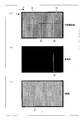
図2は、液晶パネル4を特定の駆動信号で点灯表示した際の表示状況の例を示す図面であり、エリアセンサ1はこのような表示画面を撮像することになる。検査対象の液晶パネル4の表示階調が8ビットであるとして、図2の(a)は、その中間の階調を表示させた場合(中間調画面表示モード)を表しており、図2の(b)は、「0」の状態、即ち黒画面を表示するモードの場合(黒画面表示モード)を示している。また、図2の(c)は、R画素のみを表示させているモードの場合(R画面表示モード)を示している。この外、G画面のみを表示させるG画面表示モード、B画素のみを表示させるB画面表示モード等がある。
被検査液晶パネル4の特定位置は、表示領域の左上を原点として、図に示すようなx方向(水平方向)、y方向(垂直方向)で示され、絵素数が1920(RGB)×1080の場合には、(0、0)-(5759、1079)となる。
図2に示した例の場合、欠陥は水平方向及び垂直方向の両方向の線欠陥があることを示しており、図2の(a)に示すように夫々周りの画素よりも明るいソース輝線23、24、周りの画素よりも暗いソース黒線21、ゲート黒線22がある場合を示している。なお、黒画面表示モードの図2の(b)において、中間調画面表示モードの図2の(a)中に現れていたソース輝線23が消えているが、欠陥の種類によっては、表示モードを変えることによってこのように特定の輝線が表示されなくなる場合があることを示している。同様、R画面表示モードの図2の(c)においてゲート黒線22が現れていないが、これも欠陥の種類によってこのような状況が起き得ることを示している。
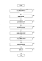
図3は、本発明に従った表示パネル点灯検査装置における線欠陥検査の手順の一例を示すフロー図である。なお、以下に説明する各処理(S1~S8)は、本発明に従った表示パネル点灯検査装置の主制御部6、及び、主制御部6の指示に基づいて検査処理部7が行うことになるが、以下の記載では、この点を省略して記載する場合がある。
図3において、検査情報取得処理(S1)では、本発明に従った表示パネル点灯検査装置の主制御部6は、CIMからパネルID、基板サイズ、画素サイズ(RGBの各1ドットを画素、RGB3ドットを1絵素と定義する)、表示領域の画素数や画素の種類等が設定されている機種情報、及び、検査レシピを取得する。但し、検査レシピは、予め検査処理部に保持しておき、パネルIDに応じて対応する検査レシピを選択し、読み込むようにしても良い。この処理は、主制御部6の指令に基づいて検査処理部7が行う。
検査レシピとしては、点灯画面切り換えデータ、バックライト出力設定値、露光時間、ゲイン設定等が含まれる撮像情報、欠陥検出用の各種設定値と検出閾値、後述する欠陥分類表等が含まれる。
画像取得処理(S2)では、主制御部6は、前記検査レシピに従って撮像された画像を取得する。即ち、点灯画面切り替えデータ等の撮像情報に基づき、エリアセンサ1によって撮像された、少なくとも1種類以上の点灯画面の画像を取得する。
線欠陥検出処理(S3)では、画像取得処理において取得した全画像を用いて線欠陥を検出する。この処理は、主制御部6の指令に基づいて検査処理部7が行う。具体的な検出処理としては、例えば、以下に図4を参照して説明する検出処理があるが、本発明は、以下に述べる検出処理に限定されるものではない。
垂直方向に発生している線欠陥の場合、図4の(a)に示すように、画像を垂直方向が一定のサイズとなるように表示領域を分割し、その分割された領域ごとに垂直方向に積算した輝度プロファイルを算出する(図4の(b)参照)。次いで、図4の(b)に示された輝度プロファイルの中で、検出閾値aを越えている部分を欠陥部とする。
この処理を被検査液晶パネルの表示部全域で行い、図4の(c)に示すように連続する欠陥部を一つの線欠陥とすることにより線欠陥を検出する。図4に示した例では、領域Aから領域Cまでは積算値が閾値を越えているので、欠陥部と判定し、領域Dは閾値を越えていないので欠陥部ではないと判定する。従って、この時の線欠陥の領域は図4の(c)に示した矩形部分となり、この矩形部分を表す情報としては、例えば、矩形の左上座標、右下座標となる。
実際の処理において、領域A、領域B等の区切りは、例えば、絵素数が1920(RGB)×1080の場合には、垂直方向に10等分(この場合には108絵素分になる)あるいは20等分程度であるがこの値に限定されるものではない。区切りが狭くなれば、線分の位置がより正確に求められるが、その分、そのための計算処理が重くなる。
線欠陥総合処理(S4)では、最初に、複数の表示モードによる複数の点灯画面で検出された線欠陥のうち、同一方向の線欠陥に注目して、これらの線欠陥を統合候補として抽出する。次いで、総合候補として抽出された線欠陥の中から、図4の(c)に示した線欠陥の座標が完全に一致、又は、一部一致する線欠陥を統合し、これを新たな一つの線欠陥とする。この段階において、表示モードに応じた欠陥分類が必要になる。
この処理が必要な理由は、以下のとおりである。即ち、被検査液晶パネルの点灯検査では、多くの種類の欠陥を検査し詳細に分類するために、複数の点灯画面を撮像し検査することから、同一の原因で発生している線欠陥でも複数の点灯場面で発生する可能性がある。従って、同一の原因で発生している線欠陥を統合し、単なる黒線や輝線という分類を行うのではなく、詳細に欠陥分類を行う必要があるためである。
断線位置検出処理(S5)では、上記の線欠陥統合処理によって統合された線欠陥の夫々について、断線により生じたものか否かを判定し、断線によるものである場合には、断線箇所の座標位置を検出する。なお、線欠陥の夫々のうち一つでも断線があれば、統合された線欠陥に断線があると判定する。この処理は、主制御部6の指令に基づいて検査処理部7が行う。なお、主制御部6の指令に基づくことなく検査処理部7が行っても良い。
この処理が必要な理由は、断線によって線欠陥の不良が発生する場合と、断線以外によって不良が発生する場合とが存在することである。
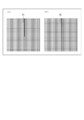
即ち、線欠陥の中には、図5の(a)に示すように線欠陥の端部が明確に存在するものと、図5の(b)のように線欠陥の端部が明確でなく、徐々に薄く消失するものがあるが、断線が存在する場合には、図5の(a)に示すように線欠陥の端部が明確に存在することが分かっている。
そして、断線がある場合には、断線部分を後のリペア工程で修復することにより、線欠陥を修復することが出来る。
従って、本発明では、前記S3の線欠陥検出処理において線欠陥として検出された「線欠陥」が、S5の断線位置検出処理において、断線に基づく線欠陥であるか否かを検出し、さらに、断線に基づく線欠陥である場合には、その断線位置を検出する。この線欠陥が断線によるものであるか否かを判定する方法、及び、断線によるものである場合に、断線位置を検出する具体的な方法は、図8を参照して後で説明する。
交点位置検出処理(S6)では、上記の線欠陥統合処理によって統合された線欠陥の夫々について、図4の(c)に示した矩形のサイズを参照して、垂直方向の線欠陥か水平方向の線欠陥かを区別する。即ち、矩形が垂直方向に長い矩形であるときは、垂直方向の線欠陥と判断し、矩形が水平方向に長い矩形であるときは、水平方向の線欠陥と判断する。さらに、方向が決定された線欠陥について、方向の異なる線欠陥の全てと順次比較し、それらの交点位置を検出する。
この線欠陥の比較は、同じモードの点灯画面、例えば図2の(c)に示すR画面表示モードで検出された線欠陥のみに限っても良いし、複数の表示モードで検出された線欠陥同士を比較しても良い。また、線欠陥の比較の結果、交点が複数存在する場合は、全ての交点を登録しても良い。複数の交点を登録することは、検査装置が複数の線欠陥を完全に分類できない場合に有効である。例えば、ソース線として種類A、ゲート線として種類Bおよび種類Cがあり、AとBとに交点が存在し、さらにAとCとに交点が存在し、なおかつパネルの特性上AおよびBの欠陥の場合には交点にリークが発生すると仮定する。この場合、「線欠陥検出処理」および「線欠陥統合処理」によって、ソース線=A、ゲート線=Bと判定されていれば、AとBとの交点1点のみを登録すればよい。しかし、BとCとの判定が付きにくい場合等には、後の工程において、両方の位置を素早く確認できるように交点2点を登録する必要がある。なお、複数登録されている場合は、後工程において優先順位を付けて確認する必要が生ずる。
この交点を求める処理(交点位置検出処理)が有効であるのは、線欠陥の中にはソースバスライン(垂直方向)とゲートバスライン(垂直方向)間のリークにより発生するものがあり、そのリーク箇所が、その交点座標部分であるためである。即ち、線欠陥の交点においては、ソースバスラインとゲートバスライン間のリークが発生している可能性が高いことになり、この交点を検出することは、前記リークを発見することにつながる。しかも、このリークは後のリペア工程で修復可能であることから、この情報は、極めて有用な情報となる。
ここまでの処理により、線欠陥データには、点灯画面情報、断線情報、交点情報が付与されていることとなる。
線欠陥分類処理(S7)では、以上に述べた各ステップでの処理で得られた線欠陥データと検査レシピとして入力された欠陥分類表を元に欠陥分類を行う。まず、図6を用いて線欠陥データの構造を説明し、次いで、図7を用いて欠陥分類について、具体例を上げて説明する。なお、図7は、欠陥分類表の一例である。
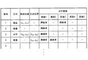
図6は、一枚の被検査液晶パネルに対する線欠陥データの構造の一例を示している。この図には、液晶パネルから実際に検出され、統合、断線検出、および交点検出を行った線欠陥についての情報を示している。図中、「点灯画面」の欄には、欠陥の有無および欠陥があった場合にはその種類(輝線または黒線)を示す情報が記載されている。
線欠陥データは、各々の線欠陥ごとに欠陥方向(垂直方向、水平方向)、断線位置、交点位置、各表示モードにおける点灯画面での検出情報の有無とから構成されている。即ち、例えば、画面1は、図2の(a)に示した中間調画面表示モードでの点灯画面であり、画面2は、図2の(b)に示した黒画面表示モードでの点灯画面であり、以下、画面3、画面4、画面5は、夫々、R画面表示モードでの点灯画面、G画面表示モードでの点灯画面、B画面表示モードでの点灯画面である。断線位置、交点位置は、画像座標、パネル座標のどちらで標記してもかまわない。図6では、交点位置を記入する場所が一箇所しか設けられていないが、これに限定されることはなく、複数の交点位置を記入できるようにしてもかまわない。
図7は、既に述べたとおり、欠陥分類表の一例であり、欠陥種類、欠陥コード、線欠陥の方向、断線があるかどうかの判定結果、交点があるかどうかの判定結果、各表示モードにおける点灯画面での検出情報の有無によって構成されている。
図7に示すとおり、例えば、「ソース断」という欠陥がある場合には、線欠陥として、垂直方向の線欠陥があり、断線の有無の判定結果は「有」であり、交点は「無」であり、線欠陥のある点灯画面は画面1と画面3であるという条件が満たされた場合であることを示している。同様、「ソースとゲート間のリーク」という欠陥がある場合には、垂直方向の線欠陥があり、断線の有無の判定結果は「無」であり、交点は「有」であり、線欠陥のある点灯画面は画面1と画面2であるという条件が満たされた場合であることを示している。
図7に示した欠陥の種類を判定するための条件、即ち、特定の欠陥とそのときの点灯画面の関係は、リペア作業におけるこれまでの経験を踏まえて決定することができるが、さらに、予め各種の欠陥を有する液晶パネルを作成しておき、この液晶パネルを各種の表示モードで実際に点灯駆動して、その際の点灯画面を分析することによって決定することもできる。
線欠陥分類処理(S7)では、図6に示す線欠陥データの1つ1つについて、欠陥分類表の1番目から付き合わせ処理を行い、合致したものにその欠陥の種類、及び、欠陥のコードを付与する。この処理において合致する欠陥の種類が存在した場合には、その線欠陥データの分類を終了し、次の線欠陥データの付き合わせ処理を開始する。欠陥分類表の最後まで付き合わせ処理を行っても合致する欠陥種類が存在しない場合には、欠陥種類、及び欠陥コードの付与を行わない。
例えば、図6における線欠陥データの番号1の欠陥の場合、「線欠陥の方向が垂直」、「断線位置が存在する」、「交点位置が存在しない」、「画面1で検出有」、「画面2で検出無し」、「画面3で検出有」、「画面4で検出無し」、「画面5で検出無し」となっていて、欠陥分類表の番号1と合致する。これにより、この欠陥を「ソース断」、「欠陥コード:S101」として分類する。
また、図6における線欠陥データの番号4の欠陥の場合、「線欠陥の方向が垂直」、「断線位置が存在しない」、「交点位置が存在する」、「画面1で検出有」、「画面2で検出有」、「画面3で検出無し」、「画面4で検出無し」、「画面5で検出無し」となっていて、欠陥分類表の番号2と合致する。これにより、この欠陥を「S-Gリーク(ソース-ゲートリーク)」、「欠陥コード:S102」として分類する。
上記の処理を全ての線欠陥データについて行い、線欠陥を分類する。この時、より正確に欠陥分類を行うために、例えば、線欠陥データ、及び、欠陥分類表にRGB画素の種類があっても良い。また、ブロック状に発生する欠陥と区別するために、欠陥方向と垂直な方向のサイズを加えても良い。また、図6、図7では点灯画面の数が5つであるがその数が制限されるものでもない。
検査対象の液晶パネルの全ての線欠陥データについて、上記線欠陥分類処理(S7)が終了すると、その結果がCIM側に出力される(S8)。既に述べたとおり、検査結果には、線欠陥の種類と欠陥の位置に関する情報が含まれている。従って、CIM側では、受け取った情報を基に、リペア可能な欠陥があった液晶パネルを、リペアのために最適なリペア工程に送ることができる。また、リペア工程では、欠陥の位置情報を受けて直ちにその場所へ顕微鏡視野を移動することも可能となり、極めて効率的な修復作業が可能となる。
次に、断線位置検出処理(S4)における、断線位置の検出について、図8を用いてその詳細を説明する。図8は、本願発明に係る表示パネル点灯検査装置における、断線の種類とその位置を求める方法の一例を説明するための図である。以下、図5の(a)、(b)に示された線欠陥を例として説明する。
図5の(a)、(b)に示された線欠陥は、垂直方向の線欠陥であるため、水平方向に一定距離はなれた正常な位置と比較し、その位置とのコントラスト値を算出する。このコントラスト値の算出は、例えば、数式(1)のような方法がある。

図5の(a)、(b)に示す垂直方向の線欠陥があった場合に、線欠陥部分を含んで水平方向に所定の画素サイズ分に渡って計算し、その結果を積算すると図8の(a)、(b)に示すようなプロファイルが得られる。なお、図8の(a)、(b)に示すグラフにおいて、縦軸はコントラストの大きさを表しており、横軸は表示画面における垂直方向の位置を表している。即ち、図8の(a)、(b)の左端部が表示画面の上端に該当し、右端部が表示画面の下端部に該当している。
ここで、図8の(a)は、垂直方向の線欠陥が断線に基づくものであることを表している状態を示しており、図8の(b)は、垂直方向の線欠陥が断線に基づくものではないことを表している状態を示している。
次いで、この図8の(a)、(b)に示すプロファイルについて、垂直方向に一定距離、離れた正常な位置と比較し、その差分を算出すると図8の(c)、(d)のプロファイルが得られる。図8の(c)、(d)に示すグラフにおいて、縦軸は差分の大きさを表し、横軸は図8の(a)、(b)と同様、表示画面における垂直方向の位置を表している。
ここで、図8の(c)は、垂直方向の線欠陥が「断線である」ことを示している状態であり、図8の(d)は、垂直方向の線欠陥が「断線ではない」ことを示している状態である。最終的に得られたプロファイルについて閾値以上(以下)の変化が存在する場合に、断線とみなし、その座標位置を断線位置であるとして登録する。
図8の例では、図8の(a)、(c)におけるプロファイルの変化の大きさに閾値を設けておき、その閾値より変化が大きいときに「断線である」と判定する。また、変化が起きている位置(垂直方向の位置)を、断線の位置と判定する。なお、上記の例の場合、表示画面の水平方向の特定位置にある垂直方向の線欠陥を問題にしているため、水平方向の位置は初めから分かっている事になる。水平方向の線欠陥の場合には、逆に、垂直方向の位置が初めから分かっていることになる。
以上の説明では、線欠陥を取り上げて説明したが、本発明は、線欠陥に限らずその他の欠陥についても適用できる。その場合、図7に記載した欠陥分類表は、これまでの種々の欠陥をリペアした経験を踏まえて作成することもできるが、予め、特定の欠陥を有する表示パネルを用意しておき、その表示パネルを種々の表示モードで点灯駆動してそのときの表示画面を分析することでも作成できる。
例えば本発明は、点欠陥にも適用できる。なお、点欠陥に適用する場合、欠陥分類表の断線および交点の情報は不要である。その代わりに、点灯画面ごとの検出状態を統合し、さらに点欠陥独自の分類を行う。
実際の表示パネルの点灯検査では、検査対象の表示パネルを、欠陥分類表を作成した時と同じ表示モードで点灯駆動し(図3のS1に相当)、その際の表示画像をエリアセンサ1で撮像し(図3のS2に相当)、取得した全画像を用いて欠陥の種類、位置等を判定する。即ち、取得した全画像の状況と、予め用意しておいた欠陥分類表と対比させることによって、欠陥の種類、欠陥の位置を判定する(S7に相当)。この場合、エリアセンサが撮像した画像そのもので分析することが困難な場合は、得られた撮像画像を微分処理等の処理を施すことも出来る。
また、既に述べたとおり、本願発明は、液晶パネルの検査に限られることなく、ELパネル、プラズマパネル等の検査にも用いることが出来る。
以上のように、本発明に係る表示パネル点灯検査装置では、表示パネルを1種類以上の表示モードで点灯駆動するための信号発生器と、点灯駆動された表示パネルの表示画像を撮像する撮像装置と、前記撮像装置によって撮像された表示パネルの点灯画面を検査および分析して欠陥に関するデータを取得する検査処理部と、前記検査処理部からの欠陥に関するデータを用いて前記表示パネルの欠陥を欠陥の種類別に分類する欠陥分類処理部とを備えた表示パネル点灯検査装置であって、前記欠陥分類処理部は、予め準備された欠陥分類表と前記検査処理部から得られた前記欠陥に関するデータとを対比して、欠陥を種類別に分類し、欠陥の種別及び欠陥の位置を出力することを特徴としている。
これによれば、表示パネルの欠陥の種別とその位置を容易に知ることが出来、リペア可能な欠陥の場合には、表示パネルをそのリペアに最適なリペア工程に送ることが出来る。
また、本発明に係る別の表示パネル点灯検査装置では、検査対象の表示パネルの機種情報及び検査レシピを受信すると共に、検査対象の表示パネルに対して前記表示パネルの機種及び検査レシピに応じた検査を自動的に行わせる制御部を備えたことを特徴としている。
これによれば、表示パネルの点灯検査を全自動化して行うことが可能になる。
また、本発明に係る別の表示パネル点灯検査装置では、前記欠陥が線欠陥であって、前記検査処理部は、少なくとも一種類以上の前記点灯画面の撮像画像から各々の点灯画面における線欠陥を検出する線欠陥検出部と、前記検出された複数の線欠陥を一つの線欠陥に統合する線欠陥統合部と、前記統合された線欠陥の夫々について、断線による欠陥か否かを検出し、断線である場合に表示パネル上における断線位置を検出する断線位置検出部と、前記統合された線欠陥の夫々について、水平方向、及び垂直方向の線欠陥の交点位置を検出する交点位置検出部と、を有することを特徴としている。
これによれば、線欠陥の種別と欠陥位置を容易に検出することが出来、リペア可能な断線欠陥あるいはリーク欠陥を有する表示パネルを最適のリペア工程に移送することが出来る。
また、本発明に係る別の表示パネル点灯検査装置では、前記複数の線欠陥を一つの線欠陥に統合する線欠陥統合部は、少なくとも、一種類以上の点灯画面で検出された線欠陥に対して、同一方向の線欠陥の中から異なる点灯画面で検出された線欠陥を統合候補として抽出する抽出部と、前記抽出された線欠陥の統合候補の中から欠陥方向に関する位置が完全、又は前記の位置が一部含有する候補を統合する統合部と、を有することを特徴としている。
これによれば、本来1つの欠陥から生じている欠陥を統合することが出来、検査をより効率的に行うことが可能となる。
また、本発明に係る別の表示パネル点灯検査装置では、前記表示パネルが液晶パネルであることを特徴としている。
これによれば、最も普及しているフラットパネルディスプレイ(FPD)である液晶パネルの欠陥を効率よく検査できる。
本願の別発明に係る表示パネル点灯検査方法では、検査対象の表示パネルを1種類以上の表示モードで点灯駆動して、点灯駆動された表示パネルの表示画像から、表示パネルの欠陥の種別と欠陥の位置を検出する表示パネル点灯検査方法であって、前記点灯駆動された表示パネルの表示画像を取得する画像取得ステップと、前記画像取得ステップによって得られた表示画像を検査および分析して欠陥に関するデータを取得する検査ステップと、予め準備された欠陥分類表と、前記検査ステップで得られた欠陥に関するデータとを比較して、欠陥を種類別に分類し、欠陥の種別及び欠陥の位置を出力するステップと、を有することを特徴としている。
これによれば、精度の高い表示パネルの点灯検査を効率よく行うことが可能となる。
また、本発明に係る別の表示パネル点灯検査方法では、前記表示パネルの欠陥は線欠陥であって、前記検査ステップは、前記画像取得ステップで取得した表示画像の線欠陥を検出する線欠陥検出ステップと、前記検出された複数の線欠陥を一つの線欠陥に統合する線欠陥統合ステップと、前記統合された線欠陥の夫々について、断線による欠陥か否かを検出し、断線による欠陥であるときには、断線位置を検出する断線位置検出ステップと、前記統合された線欠陥の夫々について、水平方向、及び垂直方向の線欠陥の交点位置を検出する交点位置検出ステップと、を有することを特徴としている。
これによれば、表示パネルの線欠陥の欠陥種別とその位置を効率よく検出することが可能となる。
本発明は上述した実施形態に限定されるものではなく、請求項に示した範囲で種々の変更が可能である。すなわち、請求項に示した範囲で適宜変更した技術的手段を組み合わせて得られる実施形態についても、本発明の技術的範囲に含まれる。
発明の詳細な説明の項においてなされた具体的な実施態様または実施例は、あくまでも、本発明の技術内容を明らかにするものであって、そのような具体例にのみ限定して狭義に解釈されるべきものではなく、本発明の精神と次に記載する特許請求事項との範囲内で、種々変更して実施することができるものである。
本発明によれば、液晶表示パネル等のFPDの製造に際して、欠陥の効率的な修復が可能となり、FPD製造における歩留まり向上に寄与することが大であって、産業上の利用可能性は極めて高い。
1 エリアセンサ(撮像装置)
2 バックライト
3 裏面偏光板
4 検査対象の液晶パネル
5 表面偏光板
6 主制御部(制御部)
7 検査処理部(欠陥分類処理部、交点位置検出部、線欠陥検出部、線欠陥統合部、断線位置検出部、抽出部、統合部)
8 信号発生器
21 ソース黒線
22 ゲート黒線
23 ソース輝線
24 ソース輝線
2 バックライト
3 裏面偏光板
4 検査対象の液晶パネル
5 表面偏光板
6 主制御部(制御部)
7 検査処理部(欠陥分類処理部、交点位置検出部、線欠陥検出部、線欠陥統合部、断線位置検出部、抽出部、統合部)
8 信号発生器
21 ソース黒線
22 ゲート黒線
23 ソース輝線
24 ソース輝線
Claims (7)
- 表示パネルを1種類以上の表示モードで点灯駆動するための信号発生器と、点灯駆動された表示パネルの表示画像を撮像する撮像装置と、前記撮像装置によって撮像された表示パネルの点灯画面を検査および分析して欠陥に関するデータを取得する検査処理部と、前記検査処理部からの欠陥に関するデータを用いて前記表示パネルの欠陥を欠陥の種類別に分類する欠陥分類処理部とを備えた表示パネル点灯検査装置であって、
前記欠陥分類処理部は、予め準備された欠陥分類表と前記検査処理部から得られた前記欠陥に関するデータとを対比して、欠陥を種類別に分類し、欠陥の種別及び欠陥の位置を出力することを特徴とする表示パネル点灯検査装置。 - 検査対象の表示パネルの機種情報及び検査レシピを受信すると共に、検査対象の表示パネルに対して前記表示パネルの機種及び検査レシピに応じた検査を自動的に行わせる制御部を備えたことを特徴とする請求項1に記載の表示パネル点灯検査装置。
- 前記欠陥が線欠陥であって、
前記検査処理部は、少なくとも一種類以上の前記点灯画面の撮像画像から各々の点灯画面における線欠陥を検出する線欠陥検出部と、
前記検出された複数の線欠陥を一つの線欠陥に統合する線欠陥統合部と、
前記統合された線欠陥の夫々について、断線による欠陥か否かを検出し、断線である場合に表示パネル上における断線位置を検出する断線位置検出部と、
前記統合された線欠陥の夫々について、水平方向、及び垂直方向の線欠陥の交点位置を検出する交点位置検出部と、有することを特徴とする請求項1又は2に記載の表示パネル点灯検査装置。 - 前記複数の線欠陥を一つの線欠陥に統合する線欠陥統合部は、
少なくとも、一種類以上の点灯画面で検出された線欠陥に対して、同一方向の線欠陥の中から異なる点灯画面で検出された線欠陥を統合候補として抽出する抽出部と、
前記抽出された線欠陥の統合候補の中から欠陥方向に関する位置が完全、又は前記の位置が一部含有する候補を統合する統合部と、
を有することを特徴とする請求項3に記載の表示パネル点灯検査装置。 - 前記表示パネルが液晶パネルであることを特徴とする請求項1から4の何れか一項に記載の表示パネル点灯検査装置。
- 検査対象の表示パネルを1種類以上の表示モードで点灯駆動して、点灯駆動された表示パネルの表示画像から、表示パネルの欠陥の種別と欠陥の位置を検出する表示パネル点灯検査方法であって、
前記点灯駆動された表示パネルの表示画像を取得する画像取得ステップと、
前記画像取得ステップによって得られた表示画像を検査および分析して欠陥に関するデータを取得する検査ステップと、
予め準備された欠陥分類表と、前記検査ステップで得られた欠陥に関するデータとを比較して、欠陥を種類別に分類し、欠陥の種別及び欠陥の位置を出力するステップと、
を有する表示パネル点灯検査方法。 - 前記表示パネルの欠陥は線欠陥であって、前記検査ステップは、
前記画像取得ステップで取得した表示画像の線欠陥を検出する線欠陥検出ステップと、
前記検出された複数の線欠陥を一つの線欠陥に統合する線欠陥統合ステップと、
前記統合された線欠陥の夫々について、断線による欠陥か否かを検出し、断線による欠陥であるときには、断線位置を検出する断線位置検出ステップと、
前記統合された線欠陥の夫々について、水平方向、及び垂直方向の線欠陥の交点位置を検出する交点位置検出ステップと、を有することを特徴とする請求項6に記載の表示パネル点灯検査方法。
Applications Claiming Priority (2)
| Application Number | Priority Date | Filing Date | Title |
|---|---|---|---|
| JP2009077284A JP4664417B2 (ja) | 2009-03-26 | 2009-03-26 | 表示パネル点灯検査装置、及び表示パネル点灯検査方法。 |
| JP2009-077284 | 2009-03-26 |
Publications (1)
| Publication Number | Publication Date |
|---|---|
| WO2010109856A1 true WO2010109856A1 (ja) | 2010-09-30 |
Family
ID=42780553
Family Applications (1)
| Application Number | Title | Priority Date | Filing Date |
|---|---|---|---|
| PCT/JP2010/002075 Ceased WO2010109856A1 (ja) | 2009-03-26 | 2010-03-24 | 表示パネル点灯検査装置、及び表示パネル点灯検査方法 |
Country Status (2)
| Country | Link |
|---|---|
| JP (1) | JP4664417B2 (ja) |
| WO (1) | WO2010109856A1 (ja) |
Cited By (2)
| Publication number | Priority date | Publication date | Assignee | Title |
|---|---|---|---|---|
| CN112213327A (zh) * | 2019-07-09 | 2021-01-12 | 陕西坤同半导体科技有限公司 | 一种显示面板人员检测辅助方法及系统 |
| WO2022246643A1 (zh) * | 2021-05-25 | 2022-12-01 | 京东方科技集团股份有限公司 | 图像获取方法及装置、存储介质 |
Families Citing this family (2)
| Publication number | Priority date | Publication date | Assignee | Title |
|---|---|---|---|---|
| CN107065247A (zh) * | 2017-06-07 | 2017-08-18 | 惠科股份有限公司 | 一种显示面板检测方法、装置及系统 |
| CN111613160A (zh) * | 2020-04-02 | 2020-09-01 | 深圳益实科技有限公司 | 一种lcd显示屏显示故障判断方法及系统 |
Citations (8)
| Publication number | Priority date | Publication date | Assignee | Title |
|---|---|---|---|---|
| JPH10197399A (ja) * | 1997-01-14 | 1998-07-31 | Sharp Corp | 薄型表示機器の欠陥箇所位置決め装置 |
| JP2006251561A (ja) * | 2005-03-11 | 2006-09-21 | Sony Corp | 欠陥画素リペア方法 |
| JP2007086056A (ja) * | 2005-08-26 | 2007-04-05 | Seiko Epson Corp | 欠陥検出方法および欠陥検出装置 |
| JP2007156338A (ja) * | 2005-12-08 | 2007-06-21 | Sharp Corp | ディスプレイパネルの修理方法 |
| JP2007315967A (ja) * | 2006-05-26 | 2007-12-06 | Sharp Corp | 欠陥検出装置、欠陥検出方法、欠陥検出プログラム、および、それを記録したコンピュータ読み取り可能な記録媒体 |
| JP2008089306A (ja) * | 2006-09-29 | 2008-04-17 | Olympus Corp | 基板検査システム、基板検査装置 |
| JP2008164336A (ja) * | 2006-12-27 | 2008-07-17 | Olympus Corp | 欠陥検査システムおよび方法 |
| JP2009031332A (ja) * | 2007-07-24 | 2009-02-12 | Sharp Corp | 透過型表示パネルの検査装置、透過型表示パネルの検査方法、透過型表示パネルの製造方法、プログラム及び記録媒体 |
-
2009
- 2009-03-26 JP JP2009077284A patent/JP4664417B2/ja active Active
-
2010
- 2010-03-24 WO PCT/JP2010/002075 patent/WO2010109856A1/ja not_active Ceased
Patent Citations (8)
| Publication number | Priority date | Publication date | Assignee | Title |
|---|---|---|---|---|
| JPH10197399A (ja) * | 1997-01-14 | 1998-07-31 | Sharp Corp | 薄型表示機器の欠陥箇所位置決め装置 |
| JP2006251561A (ja) * | 2005-03-11 | 2006-09-21 | Sony Corp | 欠陥画素リペア方法 |
| JP2007086056A (ja) * | 2005-08-26 | 2007-04-05 | Seiko Epson Corp | 欠陥検出方法および欠陥検出装置 |
| JP2007156338A (ja) * | 2005-12-08 | 2007-06-21 | Sharp Corp | ディスプレイパネルの修理方法 |
| JP2007315967A (ja) * | 2006-05-26 | 2007-12-06 | Sharp Corp | 欠陥検出装置、欠陥検出方法、欠陥検出プログラム、および、それを記録したコンピュータ読み取り可能な記録媒体 |
| JP2008089306A (ja) * | 2006-09-29 | 2008-04-17 | Olympus Corp | 基板検査システム、基板検査装置 |
| JP2008164336A (ja) * | 2006-12-27 | 2008-07-17 | Olympus Corp | 欠陥検査システムおよび方法 |
| JP2009031332A (ja) * | 2007-07-24 | 2009-02-12 | Sharp Corp | 透過型表示パネルの検査装置、透過型表示パネルの検査方法、透過型表示パネルの製造方法、プログラム及び記録媒体 |
Cited By (4)
| Publication number | Priority date | Publication date | Assignee | Title |
|---|---|---|---|---|
| CN112213327A (zh) * | 2019-07-09 | 2021-01-12 | 陕西坤同半导体科技有限公司 | 一种显示面板人员检测辅助方法及系统 |
| WO2022246643A1 (zh) * | 2021-05-25 | 2022-12-01 | 京东方科技集团股份有限公司 | 图像获取方法及装置、存储介质 |
| CN115803610A (zh) * | 2021-05-25 | 2023-03-14 | 京东方科技集团股份有限公司 | 图像获取方法及装置、存储介质 |
| US12229943B2 (en) | 2021-05-25 | 2025-02-18 | Chengdu Boe Optoelectronics Technology Co., Ltd. | Method and apparatus for acquiring images, and storage medium thereof |
Also Published As
| Publication number | Publication date |
|---|---|
| JP2010230435A (ja) | 2010-10-14 |
| JP4664417B2 (ja) | 2011-04-06 |
Similar Documents
| Publication | Publication Date | Title |
|---|---|---|
| KR101958634B1 (ko) | 디스플레이 장치의 무라 검출 장치 및 방법 | |
| KR0150689B1 (ko) | 평면형 표시패널 검사장치 | |
| JP5176014B2 (ja) | ディスプレーの多角度計測システム及び方法 | |
| KR20140091916A (ko) | 디스플레이 패널 검사방법 | |
| WO2014132506A1 (ja) | 表示パネルの欠陥検出方法及び表示パネルの欠陥検出装置 | |
| JP2007172397A (ja) | エッジ勾配検出方法、シミ欠陥検出方法、エッジ勾配検出装置、シミ欠陥検出装置 | |
| JP4664417B2 (ja) | 表示パネル点灯検査装置、及び表示パネル点灯検査方法。 | |
| JP2004212311A (ja) | ムラ欠陥の検出方法及び装置 | |
| JP3907874B2 (ja) | 欠陥検査方法 | |
| AU2022417357B2 (en) | Method of detecting defective pixels in electronic displays | |
| CN115546140A (zh) | 一种显示面板检测方法、系统及电子装置 | |
| JP3695120B2 (ja) | 欠陥検査方法 | |
| JP4804779B2 (ja) | フィルム、テープ形態の印刷回路基板外観検査における過検出防止用システム及びその処理方法 | |
| JPH04238592A (ja) | 結束棒鋼自動検数装置 | |
| KR101286548B1 (ko) | 액정표시장치의 검사 시스템 및 방법 | |
| JPH06236162A (ja) | カラー液晶パネル欠陥検査方法および装置 | |
| JP2005147911A (ja) | 表示パネルの画素評価方法及びその装置 | |
| JP2006251561A (ja) | 欠陥画素リペア方法 | |
| JP3311628B2 (ja) | 薄型表示機器の欠陥箇所位置決め装置 | |
| JP2020003219A (ja) | 表示装置の欠陥検査装置 | |
| JP2006145228A (ja) | ムラ欠陥検出方法及び装置 | |
| JP2001083474A (ja) | 液晶表示パネルの検査方法 | |
| JP2001074600A (ja) | 液晶基板の配向状態評価方法とその装置、並びに液晶基板製造モニタリング装置および液晶基板 | |
| JP3189966B2 (ja) | 液晶ディスプレイ検査装置 | |
| JPH05219535A (ja) | 液晶表示パネル検査方法 |
Legal Events
| Date | Code | Title | Description |
|---|---|---|---|
| 121 | Ep: the epo has been informed by wipo that ep was designated in this application |
Ref document number: 10755658 Country of ref document: EP Kind code of ref document: A1 |
|
| NENP | Non-entry into the national phase |
Ref country code: DE |
|
| 122 | Ep: pct application non-entry in european phase |
Ref document number: 10755658 Country of ref document: EP Kind code of ref document: A1 |