WO2010125728A1 - Cellule solaire et son procédé de fabrication - Google Patents
Cellule solaire et son procédé de fabrication Download PDFInfo
- Publication number
- WO2010125728A1 WO2010125728A1 PCT/JP2010/001394 JP2010001394W WO2010125728A1 WO 2010125728 A1 WO2010125728 A1 WO 2010125728A1 JP 2010001394 W JP2010001394 W JP 2010001394W WO 2010125728 A1 WO2010125728 A1 WO 2010125728A1
- Authority
- WO
- WIPO (PCT)
- Prior art keywords
- electrode
- passivation film
- aluminum
- back surface
- back electrode
- Prior art date
- Legal status (The legal status is an assumption and is not a legal conclusion. Google has not performed a legal analysis and makes no representation as to the accuracy of the status listed.)
- Ceased
Links
Images






Classifications
-
- H—ELECTRICITY
- H10—SEMICONDUCTOR DEVICES; ELECTRIC SOLID-STATE DEVICES NOT OTHERWISE PROVIDED FOR
- H10F—INORGANIC SEMICONDUCTOR DEVICES SENSITIVE TO INFRARED RADIATION, LIGHT, ELECTROMAGNETIC RADIATION OF SHORTER WAVELENGTH OR CORPUSCULAR RADIATION
- H10F77/00—Constructional details of devices covered by this subclass
- H10F77/20—Electrodes
- H10F77/206—Electrodes for devices having potential barriers
- H10F77/211—Electrodes for devices having potential barriers for photovoltaic cells
-
- H—ELECTRICITY
- H10—SEMICONDUCTOR DEVICES; ELECTRIC SOLID-STATE DEVICES NOT OTHERWISE PROVIDED FOR
- H10F—INORGANIC SEMICONDUCTOR DEVICES SENSITIVE TO INFRARED RADIATION, LIGHT, ELECTROMAGNETIC RADIATION OF SHORTER WAVELENGTH OR CORPUSCULAR RADIATION
- H10F10/00—Individual photovoltaic cells, e.g. solar cells
- H10F10/10—Individual photovoltaic cells, e.g. solar cells having potential barriers
- H10F10/14—Photovoltaic cells having only PN homojunction potential barriers
-
- H—ELECTRICITY
- H10—SEMICONDUCTOR DEVICES; ELECTRIC SOLID-STATE DEVICES NOT OTHERWISE PROVIDED FOR
- H10F—INORGANIC SEMICONDUCTOR DEVICES SENSITIVE TO INFRARED RADIATION, LIGHT, ELECTROMAGNETIC RADIATION OF SHORTER WAVELENGTH OR CORPUSCULAR RADIATION
- H10F71/00—Manufacture or treatment of devices covered by this subclass
- H10F71/121—The active layers comprising only Group IV materials
-
- H—ELECTRICITY
- H10—SEMICONDUCTOR DEVICES; ELECTRIC SOLID-STATE DEVICES NOT OTHERWISE PROVIDED FOR
- H10F—INORGANIC SEMICONDUCTOR DEVICES SENSITIVE TO INFRARED RADIATION, LIGHT, ELECTROMAGNETIC RADIATION OF SHORTER WAVELENGTH OR CORPUSCULAR RADIATION
- H10F77/00—Constructional details of devices covered by this subclass
- H10F77/70—Surface textures, e.g. pyramid structures
-
- H—ELECTRICITY
- H10—SEMICONDUCTOR DEVICES; ELECTRIC SOLID-STATE DEVICES NOT OTHERWISE PROVIDED FOR
- H10F—INORGANIC SEMICONDUCTOR DEVICES SENSITIVE TO INFRARED RADIATION, LIGHT, ELECTROMAGNETIC RADIATION OF SHORTER WAVELENGTH OR CORPUSCULAR RADIATION
- H10F77/00—Constructional details of devices covered by this subclass
- H10F77/70—Surface textures, e.g. pyramid structures
- H10F77/703—Surface textures, e.g. pyramid structures of the semiconductor bodies, e.g. textured active layers
-
- H—ELECTRICITY
- H10—SEMICONDUCTOR DEVICES; ELECTRIC SOLID-STATE DEVICES NOT OTHERWISE PROVIDED FOR
- H10F—INORGANIC SEMICONDUCTOR DEVICES SENSITIVE TO INFRARED RADIATION, LIGHT, ELECTROMAGNETIC RADIATION OF SHORTER WAVELENGTH OR CORPUSCULAR RADIATION
- H10F71/00—Manufacture or treatment of devices covered by this subclass
- H10F71/129—Passivating
-
- H—ELECTRICITY
- H10—SEMICONDUCTOR DEVICES; ELECTRIC SOLID-STATE DEVICES NOT OTHERWISE PROVIDED FOR
- H10F—INORGANIC SEMICONDUCTOR DEVICES SENSITIVE TO INFRARED RADIATION, LIGHT, ELECTROMAGNETIC RADIATION OF SHORTER WAVELENGTH OR CORPUSCULAR RADIATION
- H10F77/00—Constructional details of devices covered by this subclass
- H10F77/10—Semiconductor bodies
- H10F77/12—Active materials
- H10F77/122—Active materials comprising only Group IV materials
-
- H—ELECTRICITY
- H10—SEMICONDUCTOR DEVICES; ELECTRIC SOLID-STATE DEVICES NOT OTHERWISE PROVIDED FOR
- H10F—INORGANIC SEMICONDUCTOR DEVICES SENSITIVE TO INFRARED RADIATION, LIGHT, ELECTROMAGNETIC RADIATION OF SHORTER WAVELENGTH OR CORPUSCULAR RADIATION
- H10F77/00—Constructional details of devices covered by this subclass
- H10F77/10—Semiconductor bodies
- H10F77/16—Material structures, e.g. crystalline structures, film structures or crystal plane orientations
- H10F77/162—Non-monocrystalline materials, e.g. semiconductor particles embedded in insulating materials
- H10F77/164—Polycrystalline semiconductors
- H10F77/1642—Polycrystalline semiconductors including only Group IV materials
-
- Y—GENERAL TAGGING OF NEW TECHNOLOGICAL DEVELOPMENTS; GENERAL TAGGING OF CROSS-SECTIONAL TECHNOLOGIES SPANNING OVER SEVERAL SECTIONS OF THE IPC; TECHNICAL SUBJECTS COVERED BY FORMER USPC CROSS-REFERENCE ART COLLECTIONS [XRACs] AND DIGESTS
- Y02—TECHNOLOGIES OR APPLICATIONS FOR MITIGATION OR ADAPTATION AGAINST CLIMATE CHANGE
- Y02E—REDUCTION OF GREENHOUSE GAS [GHG] EMISSIONS, RELATED TO ENERGY GENERATION, TRANSMISSION OR DISTRIBUTION
- Y02E10/00—Energy generation through renewable energy sources
- Y02E10/50—Photovoltaic [PV] energy
- Y02E10/547—Monocrystalline silicon PV cells
-
- Y—GENERAL TAGGING OF NEW TECHNOLOGICAL DEVELOPMENTS; GENERAL TAGGING OF CROSS-SECTIONAL TECHNOLOGIES SPANNING OVER SEVERAL SECTIONS OF THE IPC; TECHNICAL SUBJECTS COVERED BY FORMER USPC CROSS-REFERENCE ART COLLECTIONS [XRACs] AND DIGESTS
- Y02—TECHNOLOGIES OR APPLICATIONS FOR MITIGATION OR ADAPTATION AGAINST CLIMATE CHANGE
- Y02P—CLIMATE CHANGE MITIGATION TECHNOLOGIES IN THE PRODUCTION OR PROCESSING OF GOODS
- Y02P70/00—Climate change mitigation technologies in the production process for final industrial or consumer products
- Y02P70/50—Manufacturing or production processes characterised by the final manufactured product
Definitions
- the present invention relates to a solar battery cell and a manufacturing method thereof.
- BSF Back Surface Field, hereinafter only referred to as BSF
- BSR Back Surface Reflection
- a BSF layer is formed by printing and baking an Al paste material on the entire surface of a thin, large-area substrate
- the Al paste material is printed in dots to prevent the substrate from warping or cracking.
- a planar back surface electric field layer is formed on the substrate, and a dot-like back surface electric field layer deeper than the planar back surface electrode is provided at a predetermined position on the back surface of the substrate (for example, see Patent Document 2).
- the opening of the passivation film which is the surface protection film, is formed in a dot shape, and the back reflection film is formed after the electrode is fired, or the solar cell as it is
- a plurality of cells are arranged side by side with a film or tempered glass to form an integrated solar cell module, which is placed on the back of the solar cell of the solar cell module to protect the solar cell module from ultraviolet rays, water vapor, salt, etc. It can also be configured such that the light utilization factor of a long wavelength can be increased by reflection of a back sheet which is a weather-resistant film.
- dots are formed by a printing method using a paste in which aluminum powder having a particle size of several ⁇ m, a resin, and an organic solvent are mixed. Shape and weak in structural strength. For this reason, the dot-like back electrode peels off during the surface electrode printing process up to the firing process or during transportation, and the BSF of the aluminum alloy layer or the P + layer is not sufficiently formed, increasing the contact resistance, There was a problem that the characteristics deteriorated.
- the electrode containing aluminum particles has low particle adhesion even after an electrode baking process at 700 to 800 ° C., and the series resistance component of the entire back electrode increases as the resistance component increases due to surface oxidation or the like. There was a problem that the characteristics of the cell deteriorated.
- the present invention has been made to solve such problems, and it is possible to obtain a sufficient effect of back surface protection and back surface reflection, and to obtain a back surface electrode having a large structural strength and a small resistance component. It aims at obtaining the photovoltaic cell excellent in the characteristic.
- a solar battery cell includes a semiconductor substrate, a surface uneven portion formed on a main surface on the light receiving surface side of the semiconductor substrate, and a polycrystalline semiconductor having a conductivity type formed along the surface uneven portion
- a passivation film is formed on the main surface on the back surface side of the semiconductor substrate, and at least 1 is formed on the passivation film.
- a first back electrode that overlaps with all the area occupied by the opening on the passivation film and covers the opening; and the first back electrode on the passivation film.
- a second back electrode that overlaps with all the area occupied by and covers the first back electrode.
- the present invention further includes a back electrode containing aluminum and silicon to be laminated with the aluminum back electrode, thereby increasing the structural strength, preventing electrode peeling during manufacture, and obtaining a back electrode excellent in conductivity. It is possible to obtain a solar cell that is durable and has high conversion efficiency and has both an excellent back surface protection effect and a back surface reflection effect.
- FIG. 2 is a cross-sectional view taken along the line AB shown in FIG. It is the figure which showed one form of the manufacturing process of the photovoltaic cell in Embodiment 1 of this invention. It is the figure which showed one form of the manufacturing process of the photovoltaic cell in Embodiment 1 of this invention. It is the figure which showed one form of the manufacturing process of the photovoltaic cell in Embodiment 1 of this invention. It is the figure which showed one form of the manufacturing process of the photovoltaic cell in Embodiment 1 of this invention. It is the figure which showed one form of the manufacturing process of the photovoltaic cell in Embodiment 1 of this invention.
- FIG. 1 is a perspective view (displaying a back side lower layer electrode) of a part of the solar battery cell according to Embodiment 1 of the present invention as seen from the back side.
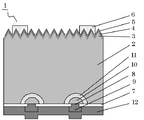
- 2 is a cross-sectional view taken along the line AB shown in FIG.
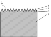
- a solar cell 1 includes a silicon substrate 2 made of p-type single crystal or polycrystal which is a semiconductor substrate, and a surface uneven portion 3 for confining light on a main surface on the light receiving surface side of the silicon substrate 2. Is formed with a depth of about 10 ⁇ m.
- an antireflection film 5 for reducing reflection and improving the light utilization rate is formed, and a photoelectric conversion unit is configured from these.
- a surface electrode 6 made of a plurality of bus electrodes orthogonal to the plurality of grid electrodes is formed on the upper surface of the antireflection film 5.
- the silicon substrate 2 is not limited to a p-type single crystal or polycrystal, and may be an n-type single crystal or polycrystal.
- a passivation film 7 that terminates silicon defects with hydrogen and suppresses recombination of minority carriers is formed.
- An opening 8 is provided in the passivation film 7.
- a dot-shaped aluminum electrode 9 as a first back electrode is formed so as to cover the opening 8 from the back surface side, and an alloy layer of aluminum and silicon by firing is formed in the silicon substrate 2 on the light receiving surface side of the aluminum electrode 9. 10 is formed.
- a BSF layer 11 which is a P + layer by aluminum diffusion is formed so as to cover the light receiving surface side of the alloy layer 10.
- an Al—Si electrode 12 which is a second back electrode, is formed so as to cover the aluminum electrode 9 and to make a line connection between the aluminum electrodes 9. Further, the BSR which is the back surface reflecting film 13 is formed so as to cover the passivation film 7, the aluminum electrode 9 and the Al—Si electrode 12 and to cover the entire main surface on the back surface side of the silicon substrate 2.
- FIGS. 3 to 12 are views showing the form of each manufacturing process of the solar battery cell of the present invention
- FIG. 13 is a flow chart showing the manufacturing process of the solar battery cell.
- S1 is start, S2 is substrate cleaning, S3 is surface etching, S4 is n-type diffusion layer formation, S5 is antireflection film formation, S6 is back surface etching, S7 is passivation film formation, S8 is opening formation, S9 is a first back electrode formation, S10 is a second back electrode formation, S11 is a surface electrode formation, S12 is a heat treatment firing, S13 is a back reflection film formation, and S14 is a completion step.
- the steps of FIGS. 3 to 12 will be described along the flow of FIG.
- a p-type polycrystalline silicon substrate is used as the silicon substrate 2, and the silicon substrate 2 is washed with hydrogen fluoride and pure water.
- the silicon substrate 2 is immersed in a mixed solution of an alkaline solution NaOH and isopropyl alcohol, and wet etching is performed so that the surface unevenness is about 10 ⁇ m, thereby forming the surface unevenness portion 3.
- a dry etching process such as RIE (reactive ion etching) is used to form irregularities of about 1 to 3 ⁇ m on the surface, or an etching mask is formed on the surface using plasma CVD, and a plurality of openings are formed there.
- hemispherical minute irregularities may be formed by etching with hydrofluoric acid. In the latter method for forming irregularities, irregularities with a regular arrangement can be formed regardless of the plane orientation of the silicon substrate 2, and the light confinement efficiency is increased.
- the n-type diffusion layer 4 is formed by thermally diffusing the silicon substrate 2 having the surface irregularities 3 on the surface in a phosphorus oxychloride (POCl 3 ) gas at a high temperature by a vapor phase diffusion method.
- concentration of phosphorus diffused can be controlled by the concentration of POCl 3 gas, the ambient temperature, the heating time, and the like.
- the sheet resistance of the substrate after diffusion is 40 to 80 ⁇ / cm 2 .
- the antireflection film 5 is formed.
- a silicon nitride film was formed to 80 nm by plasma CVD using a mixed gas of silane and ammonia.
- the process proceeds to the back electrode printing process.
- an n-type diffusion layer is also formed on the back surface in the diffusion step, so that the passivation film 7 is formed after removal by alkali etching.
- the passivation film 7 is, for example, a silicon oxide film or a vaginalized silicon film.
- the same vaginalized silicon film as the antireflection film 5 is formed with a thickness of 200 nm by the plasma CVD method.
- a plurality of openings 10 are formed in the formed passivation film 7.
- a method for forming the opening 8 there are a photoengraving method and a mechanical opening method by resist coating, exposure, and etching.
- an opening using a YAG laser (wavelength: 532 nm) that can be processed in a short time is used. I do.
- the silicon substrate 2 is adsorbed and fixed to the operating stage, the stage is moved in the X direction and the laser is moved in the Y direction, and a pattern with an opening diameter of 0.2 mm is opened at a pitch of 0.7 mm by laser irradiation.
- the pitch of the laser pattern and the opening diameter vary depending on the relationship between the electrode area and the area of the passivation film 7, a sufficient BSF layer 11 can be formed if the opening diameter is increased, and the resistance between the aluminum electrode 9 and the silicon substrate 2 is reduced. Become. On the contrary, if the opening diameter is reduced, the formation of the BSF layer 11 becomes shallower, so that the resistance between the aluminum electrode 9 and the silicon substrate 2 is increased. From the viewpoint of the passivation effect, the area of the passivation film 7 is reduced and the effect is reduced as the opening diameter is increased. On the other hand, if the opening diameter is reduced, the area of the passivation film 7 is increased and a sufficient effect can be obtained, and the values of the open circuit voltage Voc and the short circuit current Isc can be increased.
- the aluminum electrode 9 which is a 1st back surface electrode is formed in a dot shape according to the opening part 8 by the printing method.
- the aluminum electrode 9 is formed by printing a paste containing aluminum using a printing mask designed at the same position as the laser aperture pattern with a printing apparatus. At this time, the aluminum electrode 9 is formed with a diameter of about 0.3 to 0.4 mm larger than the laser aperture diameter in consideration of printing position accuracy and mask accuracy.
- the thickness of the electrode is about 20 ⁇ m.
- the printed aluminum electrode is dried at about 200 ° C.
- an Al—Si paste containing aluminum particles and silicon particles is printed on the dot-like aluminum electrode 9 so as to form an Al—Si electrode 12 as a second back electrode. Since the aluminum electrode 9 is printed so as to overlap the passivation film 7, the aluminum electrode 9 extends from the printed pattern by about 0.03 to 0.05 mm. Therefore, the size of the Al—Si electrode 12 is larger than the printing mask of the aluminum electrode 9 and has a diameter of about 0.35 to 0.45 mm, and is designed to cover the lower layer. If the Al-Si electrode 12 print mask uses the same 250 mesh specification as the aluminum electrode 9 print mask, the electrode thickness will be about 10 to 20 ⁇ m.
- the compounding ratio of aluminum particles and silicon particles in the Al—Si paste used here increases the adhesion with the aluminum electrode 9 as the mixing ratio of silicon particles increases, but the conductor resistance tends to increase.
- the composition ratio of silicon with respect to 100 parts by weight of aluminum is 5 to 20 parts by weight, but this mixing ratio is a desirable value that maintains an electrode strength that does not cause peeling and has a sufficient conductor resistance value.
- the composition ratio of silicon is 5 parts by weight or less, the electrode strength is weak, and when it is 20 parts by weight or more, the conductor resistance tends to decrease.
- the printed Al—Si electrode 12 is dried at about 200 ° C.
- front and back electrode firing is performed.
- the baking is performed at 800 ° C. using an infrared heating furnace.
- the surface electrode 6 previously formed is brought into contact with silicon by fire-through in the firing step, and the aluminum of the aluminum electrode 9 is melted with silicon as shown in FIG. Form.
- a BSF layer 11 which is a P + layer by Al diffusion is formed so as to cover the alloy layer 10.
- the film thickness of the electrode is about 20 to 25 ⁇ m, and the alloy layer 10 is formed to about 10 to 20 ⁇ m. As a result, a sufficient BSF layer 11 of about 4 to 8 ⁇ m is obtained.
- the substrate is heated in a hydrogen atmosphere at 400 ° C., and then the back reflecting film 13 is formed.
- the back reflecting film 13 was formed by sputtering to a thickness of about 500 to 1000 nm using a sputtering method.
- FIG. FIG. 14 is a perspective view (displaying the back surface side lower layer electrode) of a part of the photovoltaic cell according to Embodiment 2 of the present invention as viewed from the back surface side.
- the case where the aluminum electrode 9 has a dot shape has been described.
- the solar cell having the back surface passivation structure according to the present invention when the opening area is small in the polycrystalline silicon, However, the contact state is not stable and sufficient characteristics may not be obtained.
- the opening shape of the passivation film 7 and the electrode shape of the aluminum electrode 9 as the first back electrode are striped so as to pass through each grain boundary of the polycrystal.
- the stripe electrode 14 is used to increase the contact area.
- a dot shape may be used to increase the area occupied by the dot.
- the diameter is considerably increased. It must be large and inefficient.
- the processing pattern of the YAG laser and the pattern shape of the printing mask shown in the first embodiment are extremely changed. It can be easily handled.
- the case where the back electrode is formed in a stripe shape has been described.
- a cross shape in which lines intersect vertically and horizontally, or a circular shape or a square shape, which is slightly inferior in terms of efficiency. May be.
- a p-type polycrystalline silicon substrate having a 150 ⁇ 150 mm square and a plate thickness of 0.18 mm is used as the silicon substrate 2.
- the passivation film 7 is formed in the same manner as the first embodiment up to the step of forming the same vaginalized silicon film as the antireflection film 5 with a thickness of 200 nm by the plasma CVD method, the description is omitted.
- the surface is n-type diffused to have a sheet resistance of 50 to 60 ⁇ / cm 2 .
- a YAG laser is used for the formed passivation film 7 to remove the passivation film 7 in a stripe shape with a width of 60 ⁇ m and a pitch of 1.5 mm to form a plurality of stripe-shaped openings.
- a stripe electrode 14 having a width of 60 ⁇ m is formed by a printing method so as to cover the plurality of stripe-shaped openings.
- a silicon mixed paste in which the composition ratio of silicon is 12 parts by weight with respect to aluminum and 100 parts by weight of aluminum, a grid shape having a width of 100 ⁇ m and a pitch of 1.5 mm so as to overlap the stripe electrode 14
- an Al—Si electrode 12 is formed by a printing method.
- the surface electrode 6 is patterned by a printing method so that a plurality of thick bus electrodes having an electrode width of 2.0 mm intersect with a plurality of thin grid electrodes having an electrode width of 0.1 mm. Then, it dries at 200 ° C. and fires at 800 ° C. using an infrared heating furnace. Finally, the back reflecting film 13 is formed.
- the back reflecting film 13 was formed by sputtering to a thickness of about 800 nm using a sputtering method. In solar cell 1 formed in this way, no electrode peeling on the back surface was observed.
- the cell characteristic was measured using the sunlight simulator.
- a conventional solar battery cell was used in which the back surface was entirely coated and baked with a paste containing aluminum without the passivation film 7.
- the conventional solar cell with the entire surface aluminum electrode has the open circuit voltage Voc 620 mV, the short circuit current density Jsc 32.5 A / cm 2, the conversion efficiency E ff 16.5%, whereas the solar cell according to the second embodiment.
- the cell was confirmed to have improved photo-electron conversion efficiency with Voc 625 mV, Jsc 34.5 A / cm 2 , and conversion efficiency E ff 17.0%.
- Embodiment 3 In the first embodiment, the Al—Si paste containing aluminum particles and silicon particles is printed on the aluminum electrode, and the Al—Si electrode as the second back electrode is formed.
- An Al—Si alloy obtained by melting aluminum and silicon may be used, and a paste made of a powder obtained by granulating the alloy or a paste containing the powder may be used.
- composition ratio of aluminum and silicon in this Al—Si alloy is 5 to 20 parts by weight of silicon with respect to 100 parts by weight of aluminum as in the mixing ratio when aluminum particles and silicon particles are used.
- the reactivity to the silicon substrate is slightly lower than when using a paste made of a mixed powder of aluminum particles and silicon particles. Can do.
- 1 solar cell 2 silicon substrate, 3 surface irregularities, 4 n-type diffusion layer, 5 antireflection film, 6 surface electrode, 7 passivation film, 8 opening, 9 aluminum electrode, 10 alloy layer, 11 BSF layer, 12 Al-Si electrode, 13 back reflective film, 14 stripe electrodes
Landscapes
- Photovoltaic Devices (AREA)
Abstract
Priority Applications (4)
| Application Number | Priority Date | Filing Date | Title |
|---|---|---|---|
| CN201080018699.4A CN102414833B (zh) | 2009-04-29 | 2010-03-02 | 太阳能电池单元及其制造方法 |
| US13/266,513 US20120037224A1 (en) | 2009-04-29 | 2010-03-02 | Solar battery cell and method of manufacturing the same |
| DE112010001822T DE112010001822T8 (de) | 2009-04-29 | 2010-03-02 | Solarbatteriezelle und verfahren zu deren herstellung |
| JP2011511270A JP5152407B2 (ja) | 2009-04-29 | 2010-03-02 | 太陽電池セルおよびその製造方法 |
Applications Claiming Priority (2)
| Application Number | Priority Date | Filing Date | Title |
|---|---|---|---|
| JP2009110206 | 2009-04-29 | ||
| JP2009-110206 | 2009-04-29 |
Publications (1)
| Publication Number | Publication Date |
|---|---|
| WO2010125728A1 true WO2010125728A1 (fr) | 2010-11-04 |
Family
ID=43031888
Family Applications (1)
| Application Number | Title | Priority Date | Filing Date |
|---|---|---|---|
| PCT/JP2010/001394 Ceased WO2010125728A1 (fr) | 2009-04-29 | 2010-03-02 | Cellule solaire et son procédé de fabrication |
Country Status (5)
| Country | Link |
|---|---|
| US (1) | US20120037224A1 (fr) |
| JP (1) | JP5152407B2 (fr) |
| CN (1) | CN102414833B (fr) |
| DE (1) | DE112010001822T8 (fr) |
| WO (1) | WO2010125728A1 (fr) |
Cited By (9)
| Publication number | Priority date | Publication date | Assignee | Title |
|---|---|---|---|---|
| WO2012046306A1 (fr) * | 2010-10-05 | 2012-04-12 | 三菱電機株式会社 | Dispositif photovoltaïque et son procédé de fabrication |
| CN102610669A (zh) * | 2011-12-28 | 2012-07-25 | 友达光电股份有限公司 | 太阳能电池 |
| JP2013143499A (ja) * | 2012-01-11 | 2013-07-22 | Toyo Aluminium Kk | ペースト組成物 |
| WO2013115076A1 (fr) * | 2012-02-02 | 2013-08-08 | 東洋アルミニウム株式会社 | Composition de pâte |
| US20140158192A1 (en) * | 2012-12-06 | 2014-06-12 | Michael Cudzinovic | Seed layer for solar cell conductive contact |
| JP2016026397A (ja) * | 2011-02-15 | 2016-02-12 | サンパワー コーポレイション | 太陽電池の製造方法及び構造 |
| JP2016533635A (ja) * | 2013-09-25 | 2016-10-27 | 常州天合光能有限公司 | 結晶シリコン太陽電池の背面ブリッジ式コンタクト電極及びその製造方法 |
| JP2017028238A (ja) * | 2015-07-16 | 2017-02-02 | 有成精密股▲ふん▼有限公司 | ハイパワー太陽電池モジュール |
| CN112909105A (zh) * | 2021-02-09 | 2021-06-04 | 通威太阳能(金堂)有限公司 | 一种双面电池背面电极及其制备方法和应用 |
Families Citing this family (7)
| Publication number | Priority date | Publication date | Assignee | Title |
|---|---|---|---|---|
| TW201349255A (zh) * | 2012-02-24 | 2013-12-01 | Applied Nanotech Holdings Inc | 用於太陽能電池之金屬化糊劑 |
| KR20160034250A (ko) * | 2013-05-10 | 2016-03-29 | 에르체테 솔루션즈 게엠베하 | 태양 전지 및 그 제조 방법 |
| KR20140135881A (ko) | 2013-05-16 | 2014-11-27 | 엘지전자 주식회사 | 태양 전지 및 이의 제조 방법 |
| CN104465798A (zh) * | 2013-09-24 | 2015-03-25 | 李岱殷 | 太阳能电池结构及其形成方法 |
| JP6502651B2 (ja) | 2014-11-13 | 2019-04-17 | 信越化学工業株式会社 | 太陽電池の製造方法及び太陽電池モジュールの製造方法 |
| NL2015844B1 (en) * | 2015-11-23 | 2017-06-07 | Stichting Energieonderzoek Centrum Nederland | Enhanced metallization of silicon solar cells. |
| CN111969071B (zh) * | 2020-08-25 | 2022-03-15 | 常州时创能源股份有限公司 | 一种金属化方法和太阳能电池 |
Citations (3)
| Publication number | Priority date | Publication date | Assignee | Title |
|---|---|---|---|---|
| JP2002246625A (ja) * | 2001-02-21 | 2002-08-30 | Sharp Corp | 太陽電池の製造方法 |
| JP2007214372A (ja) * | 2006-02-09 | 2007-08-23 | Sharp Corp | 太陽電池およびその製造方法 |
| JP2008294209A (ja) * | 2007-05-24 | 2008-12-04 | Mitsubishi Electric Corp | 太陽電池基板の製造方法 |
Family Cites Families (6)
| Publication number | Priority date | Publication date | Assignee | Title |
|---|---|---|---|---|
| JPS6444277A (en) | 1987-08-11 | 1989-02-16 | Nippon Kokan Kk | Temperature control method |
| JPH01179373A (ja) | 1988-01-06 | 1989-07-17 | Hitachi Ltd | 太陽電池素子 |
| JP2007096040A (ja) * | 2005-09-29 | 2007-04-12 | Sharp Corp | 太陽電池の製造方法および太陽電池 |
| CN101840962A (zh) * | 2005-11-08 | 2010-09-22 | Lg电子株式会社 | 高效太阳能电池及其制备方法 |
| US20070169808A1 (en) * | 2006-01-26 | 2007-07-26 | Kherani Nazir P | Solar cell |
| ATE486370T1 (de) * | 2007-05-07 | 2010-11-15 | Georgia Tech Res Inst | Herstellung eines hochwertigen rückseitigen kontakts mit lokaler rückseitiger siebdruckfläche |
-
2010
- 2010-03-02 US US13/266,513 patent/US20120037224A1/en not_active Abandoned
- 2010-03-02 DE DE112010001822T patent/DE112010001822T8/de not_active Withdrawn - After Issue
- 2010-03-02 WO PCT/JP2010/001394 patent/WO2010125728A1/fr not_active Ceased
- 2010-03-02 CN CN201080018699.4A patent/CN102414833B/zh not_active Expired - Fee Related
- 2010-03-02 JP JP2011511270A patent/JP5152407B2/ja not_active Expired - Fee Related
Patent Citations (3)
| Publication number | Priority date | Publication date | Assignee | Title |
|---|---|---|---|---|
| JP2002246625A (ja) * | 2001-02-21 | 2002-08-30 | Sharp Corp | 太陽電池の製造方法 |
| JP2007214372A (ja) * | 2006-02-09 | 2007-08-23 | Sharp Corp | 太陽電池およびその製造方法 |
| JP2008294209A (ja) * | 2007-05-24 | 2008-12-04 | Mitsubishi Electric Corp | 太陽電池基板の製造方法 |
Cited By (12)
| Publication number | Priority date | Publication date | Assignee | Title |
|---|---|---|---|---|
| WO2012046306A1 (fr) * | 2010-10-05 | 2012-04-12 | 三菱電機株式会社 | Dispositif photovoltaïque et son procédé de fabrication |
| JPWO2012046306A1 (ja) * | 2010-10-05 | 2014-02-24 | 三菱電機株式会社 | 光起電力装置およびその製造方法 |
| JP2016026397A (ja) * | 2011-02-15 | 2016-02-12 | サンパワー コーポレイション | 太陽電池の製造方法及び構造 |
| CN102610669A (zh) * | 2011-12-28 | 2012-07-25 | 友达光电股份有限公司 | 太阳能电池 |
| JP2013143499A (ja) * | 2012-01-11 | 2013-07-22 | Toyo Aluminium Kk | ペースト組成物 |
| WO2013115076A1 (fr) * | 2012-02-02 | 2013-08-08 | 東洋アルミニウム株式会社 | Composition de pâte |
| JPWO2013115076A1 (ja) * | 2012-02-02 | 2015-05-11 | 東洋アルミニウム株式会社 | ペースト組成物 |
| TWI578334B (zh) * | 2012-02-02 | 2017-04-11 | 東洋鋁股份有限公司 | 糊膏狀組成物 |
| US20140158192A1 (en) * | 2012-12-06 | 2014-06-12 | Michael Cudzinovic | Seed layer for solar cell conductive contact |
| JP2016533635A (ja) * | 2013-09-25 | 2016-10-27 | 常州天合光能有限公司 | 結晶シリコン太陽電池の背面ブリッジ式コンタクト電極及びその製造方法 |
| JP2017028238A (ja) * | 2015-07-16 | 2017-02-02 | 有成精密股▲ふん▼有限公司 | ハイパワー太陽電池モジュール |
| CN112909105A (zh) * | 2021-02-09 | 2021-06-04 | 通威太阳能(金堂)有限公司 | 一种双面电池背面电极及其制备方法和应用 |
Also Published As
| Publication number | Publication date |
|---|---|
| CN102414833B (zh) | 2014-07-09 |
| CN102414833A (zh) | 2012-04-11 |
| US20120037224A1 (en) | 2012-02-16 |
| JP5152407B2 (ja) | 2013-02-27 |
| JPWO2010125728A1 (ja) | 2012-10-25 |
| DE112010001822T5 (de) | 2012-06-14 |
| DE112010001822T8 (de) | 2012-09-13 |
Similar Documents
| Publication | Publication Date | Title |
|---|---|---|
| JP5152407B2 (ja) | 太陽電池セルおよびその製造方法 | |
| JP4287473B2 (ja) | 太陽電池素子の製造方法 | |
| US20120222734A1 (en) | Solar battery cell and method of manufacturing the same | |
| CN102484148B (zh) | 太阳能电池单元及其制造方法 | |
| JP7126909B2 (ja) | バックコンタクト型太陽電池セルの製造方法 | |
| JP2016006869A (ja) | 太陽電池素子および太陽電池モジュール | |
| JP6282635B2 (ja) | 太陽電池の製造方法 | |
| WO2011074280A1 (fr) | Dispositif photovoltaïque et son procédé de préparation | |
| US20200176623A1 (en) | Solar cell element and solar cell module | |
| JP5323827B2 (ja) | 光起電力装置およびその製造方法 | |
| TWI459572B (zh) | Light power device and its manufacturing method | |
| JP5496354B2 (ja) | 光起電力装置およびその製造方法 | |
| CN103222064A (zh) | 背面电极型太阳能电池 | |
| JP2007266327A (ja) | 太陽電池素子 | |
| WO2010150358A1 (fr) | Dispositif à force photoélectromotrice, et son procédé de fabrication | |
| EP2634816A1 (fr) | Cellule de batterie solaire et son procédé de fabrication | |
| JP5452755B2 (ja) | 光起電力装置の製造方法 | |
| WO2014054605A1 (fr) | Dispositif de conversion photoélectrique, procédé de fabrication d'un dispositif de conversion photoélectrique, et module de conversion photoélectrique | |
| JP2015106585A (ja) | 太陽電池素子の製造方法および太陽電池モジュール | |
| CN103296103A (zh) | 太阳能电池单元及其制造方法 | |
| TWI753179B (zh) | 高效率內面電極型太陽電池及其製造方法 | |
| JP5501549B2 (ja) | 光電変換素子、およびそれから構成される光電変換モジュール | |
| JP6868957B2 (ja) | 光電変換素子 | |
| JP6125042B2 (ja) | 太陽電池セルの製造方法 | |
| JP4903531B2 (ja) | 太陽電池素子 |
Legal Events
| Date | Code | Title | Description |
|---|---|---|---|
| WWE | Wipo information: entry into national phase |
Ref document number: 201080018699.4 Country of ref document: CN |
|
| 121 | Ep: the epo has been informed by wipo that ep was designated in this application |
Ref document number: 10769430 Country of ref document: EP Kind code of ref document: A1 |
|
| ENP | Entry into the national phase |
Ref document number: 2011511270 Country of ref document: JP Kind code of ref document: A |
|
| WWE | Wipo information: entry into national phase |
Ref document number: 13266513 Country of ref document: US |
|
| WWE | Wipo information: entry into national phase |
Ref document number: 1120100018227 Country of ref document: DE Ref document number: 112010001822 Country of ref document: DE |
|
| 122 | Ep: pct application non-entry in european phase |
Ref document number: 10769430 Country of ref document: EP Kind code of ref document: A1 |