WO2010137217A1 - 液晶パネルおよび液晶表示装置 - Google Patents
液晶パネルおよび液晶表示装置 Download PDFInfo
- Publication number
- WO2010137217A1 WO2010137217A1 PCT/JP2010/001756 JP2010001756W WO2010137217A1 WO 2010137217 A1 WO2010137217 A1 WO 2010137217A1 JP 2010001756 W JP2010001756 W JP 2010001756W WO 2010137217 A1 WO2010137217 A1 WO 2010137217A1
- Authority
- WO
- WIPO (PCT)
- Prior art keywords
- liquid crystal
- electrode
- crystal panel
- substrate
- electric field
- Prior art date
- Legal status (The legal status is an assumption and is not a legal conclusion. Google has not performed a legal analysis and makes no representation as to the accuracy of the status listed.)
- Ceased
Links
Images


Classifications
-
- G—PHYSICS
- G02—OPTICS
- G02F—OPTICAL DEVICES OR ARRANGEMENTS FOR THE CONTROL OF LIGHT BY MODIFICATION OF THE OPTICAL PROPERTIES OF THE MEDIA OF THE ELEMENTS INVOLVED THEREIN; NON-LINEAR OPTICS; FREQUENCY-CHANGING OF LIGHT; OPTICAL LOGIC ELEMENTS; OPTICAL ANALOGUE/DIGITAL CONVERTERS
- G02F1/00—Devices or arrangements for the control of the intensity, colour, phase, polarisation or direction of light arriving from an independent light source, e.g. switching, gating or modulating; Non-linear optics
- G02F1/01—Devices or arrangements for the control of the intensity, colour, phase, polarisation or direction of light arriving from an independent light source, e.g. switching, gating or modulating; Non-linear optics for the control of the intensity, phase, polarisation or colour
- G02F1/13—Devices or arrangements for the control of the intensity, colour, phase, polarisation or direction of light arriving from an independent light source, e.g. switching, gating or modulating; Non-linear optics for the control of the intensity, phase, polarisation or colour based on liquid crystals, e.g. single liquid crystal display cells
- G02F1/133—Constructional arrangements; Operation of liquid crystal cells; Circuit arrangements
- G02F1/1333—Constructional arrangements; Manufacturing methods
- G02F1/1343—Electrodes
- G02F1/134309—Electrodes characterised by their geometrical arrangement
- G02F1/134363—Electrodes characterised by their geometrical arrangement for applying an electric field parallel to the substrate, i.e. in-plane switching [IPS]
-
- G—PHYSICS
- G09—EDUCATION; CRYPTOGRAPHY; DISPLAY; ADVERTISING; SEALS
- G09G—ARRANGEMENTS OR CIRCUITS FOR CONTROL OF INDICATING DEVICES USING STATIC MEANS TO PRESENT VARIABLE INFORMATION
- G09G3/00—Control arrangements or circuits, of interest only in connection with visual indicators other than cathode-ray tubes
- G09G3/20—Control arrangements or circuits, of interest only in connection with visual indicators other than cathode-ray tubes for presentation of an assembly of a number of characters, e.g. a page, by composing the assembly by combination of individual elements arranged in a matrix no fixed position being assigned to or needed to be assigned to the individual characters or partial characters
- G09G3/34—Control arrangements or circuits, of interest only in connection with visual indicators other than cathode-ray tubes for presentation of an assembly of a number of characters, e.g. a page, by composing the assembly by combination of individual elements arranged in a matrix no fixed position being assigned to or needed to be assigned to the individual characters or partial characters by control of light from an independent source
- G09G3/36—Control arrangements or circuits, of interest only in connection with visual indicators other than cathode-ray tubes for presentation of an assembly of a number of characters, e.g. a page, by composing the assembly by combination of individual elements arranged in a matrix no fixed position being assigned to or needed to be assigned to the individual characters or partial characters by control of light from an independent source using liquid crystals
- G09G3/3611—Control of matrices with row and column drivers
- G09G3/3648—Control of matrices with row and column drivers using an active matrix
- G09G3/3659—Control of matrices with row and column drivers using an active matrix the addressing of the pixel involving the control of two or more scan electrodes or two or more data electrodes, e.g. pixel voltage dependant on signal of two data electrodes
-
- G—PHYSICS
- G02—OPTICS
- G02F—OPTICAL DEVICES OR ARRANGEMENTS FOR THE CONTROL OF LIGHT BY MODIFICATION OF THE OPTICAL PROPERTIES OF THE MEDIA OF THE ELEMENTS INVOLVED THEREIN; NON-LINEAR OPTICS; FREQUENCY-CHANGING OF LIGHT; OPTICAL LOGIC ELEMENTS; OPTICAL ANALOGUE/DIGITAL CONVERTERS
- G02F1/00—Devices or arrangements for the control of the intensity, colour, phase, polarisation or direction of light arriving from an independent light source, e.g. switching, gating or modulating; Non-linear optics
- G02F1/01—Devices or arrangements for the control of the intensity, colour, phase, polarisation or direction of light arriving from an independent light source, e.g. switching, gating or modulating; Non-linear optics for the control of the intensity, phase, polarisation or colour
- G02F1/13—Devices or arrangements for the control of the intensity, colour, phase, polarisation or direction of light arriving from an independent light source, e.g. switching, gating or modulating; Non-linear optics for the control of the intensity, phase, polarisation or colour based on liquid crystals, e.g. single liquid crystal display cells
- G02F1/133—Constructional arrangements; Operation of liquid crystal cells; Circuit arrangements
- G02F1/1333—Constructional arrangements; Manufacturing methods
- G02F1/1337—Surface-induced orientation of the liquid crystal molecules, e.g. by alignment layers
- G02F1/133742—Surface-induced orientation of the liquid crystal molecules, e.g. by alignment layers for homeotropic alignment
-
- G—PHYSICS
- G02—OPTICS
- G02F—OPTICAL DEVICES OR ARRANGEMENTS FOR THE CONTROL OF LIGHT BY MODIFICATION OF THE OPTICAL PROPERTIES OF THE MEDIA OF THE ELEMENTS INVOLVED THEREIN; NON-LINEAR OPTICS; FREQUENCY-CHANGING OF LIGHT; OPTICAL LOGIC ELEMENTS; OPTICAL ANALOGUE/DIGITAL CONVERTERS
- G02F1/00—Devices or arrangements for the control of the intensity, colour, phase, polarisation or direction of light arriving from an independent light source, e.g. switching, gating or modulating; Non-linear optics
- G02F1/01—Devices or arrangements for the control of the intensity, colour, phase, polarisation or direction of light arriving from an independent light source, e.g. switching, gating or modulating; Non-linear optics for the control of the intensity, phase, polarisation or colour
- G02F1/13—Devices or arrangements for the control of the intensity, colour, phase, polarisation or direction of light arriving from an independent light source, e.g. switching, gating or modulating; Non-linear optics for the control of the intensity, phase, polarisation or colour based on liquid crystals, e.g. single liquid crystal display cells
- G02F1/133—Constructional arrangements; Operation of liquid crystal cells; Circuit arrangements
- G02F1/1333—Constructional arrangements; Manufacturing methods
- G02F1/1343—Electrodes
- G02F1/134309—Electrodes characterised by their geometrical arrangement
- G02F1/134372—Electrodes characterised by their geometrical arrangement for fringe field switching [FFS] where the common electrode is not patterned
-
- G—PHYSICS
- G02—OPTICS
- G02F—OPTICAL DEVICES OR ARRANGEMENTS FOR THE CONTROL OF LIGHT BY MODIFICATION OF THE OPTICAL PROPERTIES OF THE MEDIA OF THE ELEMENTS INVOLVED THEREIN; NON-LINEAR OPTICS; FREQUENCY-CHANGING OF LIGHT; OPTICAL LOGIC ELEMENTS; OPTICAL ANALOGUE/DIGITAL CONVERTERS
- G02F1/00—Devices or arrangements for the control of the intensity, colour, phase, polarisation or direction of light arriving from an independent light source, e.g. switching, gating or modulating; Non-linear optics
- G02F1/01—Devices or arrangements for the control of the intensity, colour, phase, polarisation or direction of light arriving from an independent light source, e.g. switching, gating or modulating; Non-linear optics for the control of the intensity, phase, polarisation or colour
- G02F1/13—Devices or arrangements for the control of the intensity, colour, phase, polarisation or direction of light arriving from an independent light source, e.g. switching, gating or modulating; Non-linear optics for the control of the intensity, phase, polarisation or colour based on liquid crystals, e.g. single liquid crystal display cells
- G02F1/133—Constructional arrangements; Operation of liquid crystal cells; Circuit arrangements
- G02F1/1333—Constructional arrangements; Manufacturing methods
- G02F1/1343—Electrodes
- G02F1/134309—Electrodes characterised by their geometrical arrangement
- G02F1/134381—Hybrid switching mode, i.e. for applying an electric field with components parallel and orthogonal to the substrates
-
- G—PHYSICS
- G02—OPTICS
- G02F—OPTICAL DEVICES OR ARRANGEMENTS FOR THE CONTROL OF LIGHT BY MODIFICATION OF THE OPTICAL PROPERTIES OF THE MEDIA OF THE ELEMENTS INVOLVED THEREIN; NON-LINEAR OPTICS; FREQUENCY-CHANGING OF LIGHT; OPTICAL LOGIC ELEMENTS; OPTICAL ANALOGUE/DIGITAL CONVERTERS
- G02F1/00—Devices or arrangements for the control of the intensity, colour, phase, polarisation or direction of light arriving from an independent light source, e.g. switching, gating or modulating; Non-linear optics
- G02F1/01—Devices or arrangements for the control of the intensity, colour, phase, polarisation or direction of light arriving from an independent light source, e.g. switching, gating or modulating; Non-linear optics for the control of the intensity, phase, polarisation or colour
- G02F1/13—Devices or arrangements for the control of the intensity, colour, phase, polarisation or direction of light arriving from an independent light source, e.g. switching, gating or modulating; Non-linear optics for the control of the intensity, phase, polarisation or colour based on liquid crystals, e.g. single liquid crystal display cells
- G02F1/133—Constructional arrangements; Operation of liquid crystal cells; Circuit arrangements
- G02F1/136—Liquid crystal cells structurally associated with a semi-conducting layer or substrate, e.g. cells forming part of an integrated circuit
- G02F1/1362—Active matrix addressed cells
- G02F1/13624—Active matrix addressed cells having more than one switching element per pixel
-
- G—PHYSICS
- G02—OPTICS
- G02F—OPTICAL DEVICES OR ARRANGEMENTS FOR THE CONTROL OF LIGHT BY MODIFICATION OF THE OPTICAL PROPERTIES OF THE MEDIA OF THE ELEMENTS INVOLVED THEREIN; NON-LINEAR OPTICS; FREQUENCY-CHANGING OF LIGHT; OPTICAL LOGIC ELEMENTS; OPTICAL ANALOGUE/DIGITAL CONVERTERS
- G02F1/00—Devices or arrangements for the control of the intensity, colour, phase, polarisation or direction of light arriving from an independent light source, e.g. switching, gating or modulating; Non-linear optics
- G02F1/01—Devices or arrangements for the control of the intensity, colour, phase, polarisation or direction of light arriving from an independent light source, e.g. switching, gating or modulating; Non-linear optics for the control of the intensity, phase, polarisation or colour
- G02F1/13—Devices or arrangements for the control of the intensity, colour, phase, polarisation or direction of light arriving from an independent light source, e.g. switching, gating or modulating; Non-linear optics for the control of the intensity, phase, polarisation or colour based on liquid crystals, e.g. single liquid crystal display cells
- G02F1/137—Devices or arrangements for the control of the intensity, colour, phase, polarisation or direction of light arriving from an independent light source, e.g. switching, gating or modulating; Non-linear optics for the control of the intensity, phase, polarisation or colour based on liquid crystals, e.g. single liquid crystal display cells characterised by the electro-optical or magneto-optical effect, e.g. field-induced phase transition, orientation effect, guest-host interaction or dynamic scattering
- G02F1/13706—Devices or arrangements for the control of the intensity, colour, phase, polarisation or direction of light arriving from an independent light source, e.g. switching, gating or modulating; Non-linear optics for the control of the intensity, phase, polarisation or colour based on liquid crystals, e.g. single liquid crystal display cells characterised by the electro-optical or magneto-optical effect, e.g. field-induced phase transition, orientation effect, guest-host interaction or dynamic scattering the liquid crystal having positive dielectric anisotropy
-
- G—PHYSICS
- G02—OPTICS
- G02F—OPTICAL DEVICES OR ARRANGEMENTS FOR THE CONTROL OF LIGHT BY MODIFICATION OF THE OPTICAL PROPERTIES OF THE MEDIA OF THE ELEMENTS INVOLVED THEREIN; NON-LINEAR OPTICS; FREQUENCY-CHANGING OF LIGHT; OPTICAL LOGIC ELEMENTS; OPTICAL ANALOGUE/DIGITAL CONVERTERS
- G02F1/00—Devices or arrangements for the control of the intensity, colour, phase, polarisation or direction of light arriving from an independent light source, e.g. switching, gating or modulating; Non-linear optics
- G02F1/01—Devices or arrangements for the control of the intensity, colour, phase, polarisation or direction of light arriving from an independent light source, e.g. switching, gating or modulating; Non-linear optics for the control of the intensity, phase, polarisation or colour
- G02F1/13—Devices or arrangements for the control of the intensity, colour, phase, polarisation or direction of light arriving from an independent light source, e.g. switching, gating or modulating; Non-linear optics for the control of the intensity, phase, polarisation or colour based on liquid crystals, e.g. single liquid crystal display cells
- G02F1/137—Devices or arrangements for the control of the intensity, colour, phase, polarisation or direction of light arriving from an independent light source, e.g. switching, gating or modulating; Non-linear optics for the control of the intensity, phase, polarisation or colour based on liquid crystals, e.g. single liquid crystal display cells characterised by the electro-optical or magneto-optical effect, e.g. field-induced phase transition, orientation effect, guest-host interaction or dynamic scattering
- G02F1/139—Devices or arrangements for the control of the intensity, colour, phase, polarisation or direction of light arriving from an independent light source, e.g. switching, gating or modulating; Non-linear optics for the control of the intensity, phase, polarisation or colour based on liquid crystals, e.g. single liquid crystal display cells characterised by the electro-optical or magneto-optical effect, e.g. field-induced phase transition, orientation effect, guest-host interaction or dynamic scattering based on orientation effects in which the liquid crystal remains transparent
- G02F1/1393—Devices or arrangements for the control of the intensity, colour, phase, polarisation or direction of light arriving from an independent light source, e.g. switching, gating or modulating; Non-linear optics for the control of the intensity, phase, polarisation or colour based on liquid crystals, e.g. single liquid crystal display cells characterised by the electro-optical or magneto-optical effect, e.g. field-induced phase transition, orientation effect, guest-host interaction or dynamic scattering based on orientation effects in which the liquid crystal remains transparent the birefringence of the liquid crystal being electrically controlled, e.g. ECB-, DAP-, HAN-, PI-LC cells
- G02F1/1395—Optically compensated birefringence [OCB]- cells or PI- cells
-
- G—PHYSICS
- G02—OPTICS
- G02F—OPTICAL DEVICES OR ARRANGEMENTS FOR THE CONTROL OF LIGHT BY MODIFICATION OF THE OPTICAL PROPERTIES OF THE MEDIA OF THE ELEMENTS INVOLVED THEREIN; NON-LINEAR OPTICS; FREQUENCY-CHANGING OF LIGHT; OPTICAL LOGIC ELEMENTS; OPTICAL ANALOGUE/DIGITAL CONVERTERS
- G02F2201/00—Constructional arrangements not provided for in groups G02F1/00 - G02F7/00
- G02F2201/12—Constructional arrangements not provided for in groups G02F1/00 - G02F7/00 electrode
- G02F2201/124—Constructional arrangements not provided for in groups G02F1/00 - G02F7/00 electrode interdigital
-
- G—PHYSICS
- G09—EDUCATION; CRYPTOGRAPHY; DISPLAY; ADVERTISING; SEALS
- G09G—ARRANGEMENTS OR CIRCUITS FOR CONTROL OF INDICATING DEVICES USING STATIC MEANS TO PRESENT VARIABLE INFORMATION
- G09G2300/00—Aspects of the constitution of display devices
- G09G2300/04—Structural and physical details of display devices
- G09G2300/0421—Structural details of the set of electrodes
- G09G2300/0426—Layout of electrodes and connections
-
- G—PHYSICS
- G09—EDUCATION; CRYPTOGRAPHY; DISPLAY; ADVERTISING; SEALS
- G09G—ARRANGEMENTS OR CIRCUITS FOR CONTROL OF INDICATING DEVICES USING STATIC MEANS TO PRESENT VARIABLE INFORMATION
- G09G2300/00—Aspects of the constitution of display devices
- G09G2300/04—Structural and physical details of display devices
- G09G2300/0421—Structural details of the set of electrodes
- G09G2300/0434—Flat panel display in which a field is applied parallel to the display plane
-
- G—PHYSICS
- G09—EDUCATION; CRYPTOGRAPHY; DISPLAY; ADVERTISING; SEALS
- G09G—ARRANGEMENTS OR CIRCUITS FOR CONTROL OF INDICATING DEVICES USING STATIC MEANS TO PRESENT VARIABLE INFORMATION
- G09G2300/00—Aspects of the constitution of display devices
- G09G2300/04—Structural and physical details of display devices
- G09G2300/0469—Details of the physics of pixel operation
- G09G2300/0478—Details of the physics of pixel operation related to liquid crystal pixels
- G09G2300/0491—Use of a bi-refringent liquid crystal, optically controlled bi-refringence [OCB] with bend and splay states, or electrically controlled bi-refringence [ECB] for controlling the color
-
- G—PHYSICS
- G09—EDUCATION; CRYPTOGRAPHY; DISPLAY; ADVERTISING; SEALS
- G09G—ARRANGEMENTS OR CIRCUITS FOR CONTROL OF INDICATING DEVICES USING STATIC MEANS TO PRESENT VARIABLE INFORMATION
- G09G2300/00—Aspects of the constitution of display devices
- G09G2300/08—Active matrix structure, i.e. with use of active elements, inclusive of non-linear two terminal elements, in the pixels together with light emitting or modulating elements
- G09G2300/0809—Several active elements per pixel in active matrix panels
- G09G2300/0814—Several active elements per pixel in active matrix panels used for selection purposes, e.g. logical AND for partial update
-
- G—PHYSICS
- G09—EDUCATION; CRYPTOGRAPHY; DISPLAY; ADVERTISING; SEALS
- G09G—ARRANGEMENTS OR CIRCUITS FOR CONTROL OF INDICATING DEVICES USING STATIC MEANS TO PRESENT VARIABLE INFORMATION
- G09G2300/00—Aspects of the constitution of display devices
- G09G2300/08—Active matrix structure, i.e. with use of active elements, inclusive of non-linear two terminal elements, in the pixels together with light emitting or modulating elements
- G09G2300/0809—Several active elements per pixel in active matrix panels
- G09G2300/0842—Several active elements per pixel in active matrix panels forming a memory circuit, e.g. a dynamic memory with one capacitor
Definitions
- the present invention relates to a liquid crystal panel and a liquid crystal display device, and more particularly to a liquid crystal panel and a liquid crystal display device which control light transmission by bending a liquid crystal layer by applying a voltage.
- Liquid crystal display devices are characterized by thinness, light weight, and low power consumption, and are widely used in various fields.
- the display performance of the liquid crystal display device has been remarkably improved with the passage of time, and has now surpassed that of a CRT (cathode ray tube).
- the display method of the liquid crystal display device is determined by how the liquid crystals are arranged in the liquid crystal cell.
- Various display systems are known as display systems for liquid crystal display devices. One of them is a display method in which an electric field parallel to the substrate surface (so-called lateral electric field) is applied to a vertical alignment cell in which liquid crystal molecules are aligned vertically to the substrate when no voltage is applied. There is.
- the orientation direction of liquid crystal molecules is defined by being driven by a horizontal electric field while maintaining high contrast by vertical alignment. For this reason, the said display system has the outstanding viewing angle characteristic.
- Non-Patent Document 1 discloses a display method called a VA-IPS mode.
- Non-Patent Document 1 discloses that the VA-IPS mode has little color shift depending on the viewing angle.
- FIG. 17A is a cross-sectional view schematically showing a schematic configuration of a main part of a liquid crystal cell using the VA-IPS mode described in Non-Patent Document 1, and FIG. It is a timing chart of the applied voltage in each electrode shown to (a).
- the liquid crystal cell described in Non-Patent Document 1 has a solid common electrode on a substrate 311 facing a substrate 301 provided with pixel electrodes 302 and 303 as comb-like electrodes. 312 is provided.
- a lateral electric field is applied to the liquid crystal cell by applying voltages having opposite phases to the pixel electrode 302 and the pixel electrode 303.
- the display method in which a lateral electric field is applied to the vertically aligned cells has a problem that the light transmittance is low while having high contrast and excellent viewing angle characteristics due to the vertical alignment as described above.
- the present situation is that the liquid crystal panel and the liquid crystal display device using the display method have not been put into practical use.
- the present invention has been made in view of the above-mentioned problems, and the object thereof is a liquid crystal panel capable of obtaining a practical light transmittance in a display method in which a lateral electric field is applied to a vertically aligned cell as described above. Another object is to provide a liquid crystal display device.
- the inventors of the present application arbitrarily control the degree of bend alignment (the degree of bending of bend-aligned p-type liquid crystal molecules) by changing the panel configuration and the physical properties of the liquid crystal material used. It has been found that practical light transmittance can be obtained by controlling the degree of bend alignment.
- the liquid crystal panel according to the present invention includes a liquid crystal material sandwiched between a pair of substrates and a comb-like electrode, and applies an electric field parallel to the substrate surface to the liquid crystal material.
- the electrode spacing is 15 ⁇ m or less, and a voltage of 7 V or more is applied between the electrodes for applying an electric field parallel to the substrate surface to the liquid crystal material during driving, and the dielectric anisotropy of the p-type liquid crystal material
- the product ( ⁇ ⁇ ⁇ n) of ⁇ and refractive index anisotropy ⁇ n is 0.9 or more and 2.5 or less.
- applying an electric field parallel to the substrate surface means “applying an electric field having at least a component parallel to the substrate surface”.
- the p-type liquid crystal material is aligned perpendicularly to the substrate surface means “the p-type liquid crystal material has at least an alignment component perpendicular to the substrate surface”. That is, “parallel” and “vertical” include “substantially parallel” and “substantially vertical”.
- the liquid crystal panel according to the present invention uses a display method in which a horizontal electric field is applied to a vertically aligned cell in which liquid crystal molecules are vertically aligned when driven (when a voltage is applied). For this reason, it has the advantages of being able to obtain high-speed response based on bend alignment, a wide viewing angle due to a self-compensating arrangement, and high contrast due to vertical alignment, simple structure, easy manufacturing, and low cost. It has the advantage that it can be manufactured.
- a liquid crystal panel using such a display method has the above-mentioned advantages, but has a problem that the transmittance is low in principle.
- the display method in which a lateral electric field is applied to the vertical alignment cell as described above is practically more than 60%. It is possible to obtain a transmittance and use a liquid crystal material having a large dielectric anisotropy ⁇ .
- the liquid crystal viscosity can be reduced, so that a high-speed response can be realized with certainty.
- the panel phase difference ⁇ nd is increased, the viewing angle characteristic is deteriorated. Therefore, practically, it is desirable to increase ⁇ within a range in which reliability is not lowered, rather than increasing ⁇ n. Therefore, according to the present invention, it is possible to improve transmittance and response speed while maintaining viewing angle characteristics and reliability.
- the transmittance is higher than the conventional one, and the wide viewing angle characteristic equivalent to that of the MVA mode or the IPS mode, the high speed response equivalent to or higher than the OCB mode, and the high contrast characteristic. It is possible to provide a practical liquid crystal panel that can realize the above simultaneously.
- the liquid crystal display device according to the present invention is characterized by including the liquid crystal panel according to the present invention in order to solve the above-described problems.
- the liquid crystal panel and the liquid crystal display device according to the present invention are driven by a so-called lateral electric field parallel to the substrate surface while maintaining high contrast due to vertical alignment, thereby achieving a wide field of view with a simple pixel configuration.
- Angular characteristics as well as high contrast characteristics can be realized.
- an initial bend transition operation is unnecessary, and a practical bend alignment can be realized.
- the electrode that applies an electric field parallel to the substrate surface to the liquid crystal material includes the comb-like electrode as described above, the electrode width of the comb-like electrode is 5 ⁇ m or less, and the electrode interval is 15 ⁇ m or less.
- a voltage of 7 V or more is applied between electrodes that apply an electric field parallel to the substrate surface to the liquid crystal material, and the dielectric anisotropy ⁇ and refractive index anisotropy ⁇ n of the p-type liquid crystal material.
- the product ( ⁇ ⁇ ⁇ n) is 0.9 or more and 2.5 or less, a practical transmittance exceeding 60% can be obtained, and a liquid crystal material having a large dielectric anisotropy ⁇ is used. It becomes possible to do.
- the viscosity of the liquid crystal can be reduced, a high-speed response can be realized reliably.
- the liquid crystal material having a large dielectric anisotropy ⁇ can be used as described above, the transmittance and the response speed can be improved while maintaining the viewing angle characteristics and the reliability.
- FIG. 1 is an exploded sectional view schematically showing an example of a schematic configuration of a liquid crystal display device according to the present invention. It is a disassembled perspective view which shows typically the basic composition of the liquid crystal panel driven by the display system of this invention. It is sectional drawing which shows typically the basic composition of the liquid crystal panel driven with the display system of this invention. It is a figure which shows the relationship between the transmission axis direction of the polarizing plate of the liquid crystal panel shown in FIG. 4, and an electric field application direction.
- FIG. 4 (a) is a perspective view of the principal part of the said liquid crystal panel at the time of no electric field application.
- FIG. 6B is a perspective view of the main part of the liquid crystal panel when an electric field is applied. It is a figure which shows an example of the director distribution of the p-type liquid crystal molecule in this liquid crystal cell when the voltage of 3.5V is applied to the liquid crystal cell using the display system of this invention. It is a graph which shows an example of the relationship between the transmittance
- FIG. 8 is a graph showing a transmittance distribution and a phase difference distribution in a liquid crystal cell having different electrode intervals.
- A is sectional drawing which shows typically schematic structure of the principal part of the liquid crystal panel concerning other embodiment of this invention
- (b) is a timing chart of the applied voltage in each electrode shown to (a) It is.
- FIG. 11 is a diagram showing a director distribution and equipotential curves of p-type liquid crystal molecules in a liquid crystal cell when a voltage of +6 V or ⁇ 6 V is applied to the pixel electrodes shown in FIGS. It is sectional drawing which shows typically schematic structure of the principal part of the liquid crystal panel concerning further another embodiment of this invention.
- FIG. 15 is a timing chart of applied voltages applied to the pixel electrode, the gate line, and the common electrode shown in FIG. 14.
- A is sectional drawing which shows typically schematic structure of the principal part of the liquid crystal cell using the VA-IPS mode of a nonpatent literature 1
- b is each electrode shown to (a). It is a timing chart of an applied voltage.
- an electric field (lateral electric field) parallel to the substrate surface is applied to a vertically aligned cell using a comb-like electrode having a comb-like structure, thereby forming a bow-like shape (bend shape) in the cell.
- Liquid crystal alignment distribution hereinafter referred to as “main mode”.
- FIG. 2 is an exploded sectional view schematically showing an example of a schematic configuration of the liquid crystal display device according to the present invention.
- FIG. 3 is an exploded perspective view schematically showing the basic configuration of the liquid crystal panel driven in this mode.
- FIG. 4 is a cross-sectional view schematically showing a basic configuration of a liquid crystal panel driven in this mode.
- the display surface side (observer side substrate) is described as the upper substrate, and the other substrate is described as the lower substrate.
- the liquid crystal display device 1 includes a liquid crystal panel 2, a drive circuit 3, and a backlight 4 (illumination device).
- the configuration of the drive circuit 3 and the backlight 4 is the same as the conventional one. Therefore, the description of these configurations is omitted.
- the liquid crystal panel 2 includes an electrode substrate (array substrate, element substrate) and a pair of substrates 10 and 20 provided to face each other as an opposing substrate.
- a liquid crystal layer 30 containing a p-type liquid crystal material is sandwiched between the pair of substrates 10 and 20 as a display medium layer.
- Each of the pair of substrates 10 and 20 includes an insulating substrate having an insulating property. At least one of the pair of substrates 10 and 20 includes a transparent substrate such as a glass substrate as the insulating substrate.
- the pair of substrates 10 and 20 will be described as including the glass substrates 11 and 21 as insulating substrates, but the present invention is not limited to this.
- alignment films 12 and 22 are respectively provided on the surfaces of the pair of substrates 10 and 20 facing the other substrate.
- the vertical alignment film is an alignment film that aligns the liquid crystal molecules of the liquid crystal layer perpendicularly to the substrate surface when no electric field is applied.
- the “vertical” includes “substantially vertical”.
- the p-type liquid crystal molecules 31 in the liquid crystal layer 30 exhibit homeotropic alignment as shown in FIG. 3 when no voltage is applied. Note that the p-type liquid crystal molecules 31 continuously change from homeotropic alignment to bend alignment by voltage application. That is, in normal driving, the liquid crystal layer 30 always exhibits a bend alignment, and a high-speed response is possible with an inter-tone response.
- one of the substrates 10 and 20 includes an electric field applying unit for applying an electric field parallel to the substrate surface, which is referred to as a so-called lateral electric field, to the liquid crystal layer 30. Yes.
- the “parallel” includes “substantially parallel”.
- the substrates 10 and 20 include the glass substrates 11 and 21, respectively, as described above.
- a pixel electrode 13 and a common electrode 14 are provided on the glass substrate 11 of the substrate 10 as an electric field applying means for applying a lateral electric field to the liquid crystal layer 30.
- At least one of the pixel electrode 13 and the common electrode 14 has a comb-like structure as described above.
- the pixel electrode 13 and the common electrode 14 may be made of a transparent electrode material such as ITO (indium tin oxide), or may be made of a metal such as aluminum.
- the material of the pixel electrode 13 and the common electrode 14 is not particularly limited.
- the alignment film 12 is provided so as to cover the pixel electrode 13 and the common electrode 14.
- the material and formation method of the alignment films 12 and 22 are not particularly limited.
- the alignment films 12 and 22 can be formed, for example, by applying a known alignment film material having a vertical alignment regulating force on the pixel electrode 13 and the common electrode 14.
- an array substrate such as a TFT array substrate, a color filter substrate, or the like can be used, but the present invention is not limited to this.
- polarizing plates 35 and 36 are provided on the surfaces of the pair of substrates 10 and 20 opposite to the surfaces facing the liquid crystal layer 30, respectively.
- retardation plates 37 and 38 are provided between the substrates 10 and 20 and the polarizing plates 35 and 36, respectively, as necessary.
- the retardation plates 37 and 38 may be provided only on one surface of the liquid crystal panel 2.
- the phase difference plates 37 and 38 are not necessarily essential.
- the liquid crystal cell 5 in the liquid crystal panel 2 includes, for example, as shown in FIG. 4, the substrate 10 and the substrate 20 are bonded together with a sealant 34 via a spacer 33, and a gap between the substrates 10 and 20 is formed. It is formed by enclosing a medium containing a p-type liquid crystal material as the liquid crystal material.
- the p-type liquid crystal material include a p-type nematic liquid crystal material.
- the liquid crystal panel 2 is formed by bonding the phase difference plates 37 and 38 and the polarizing plates 35 and 36 to the liquid crystal cell 5 as described above.
- FIG. 5 shows the relationship between the transmission axis direction of the polarizing plates 35 and 36 and the electric field application direction.
- the polarizing plates 35 and 36 are arranged such that the transmission axis directions of the polarizing plates 35 and 36 are orthogonal to each other and form 45 degrees with the electric field application direction.
- 6 (a) and 6 (b) show how the p-type liquid crystal molecules 31 are rotated by applying an electric field in this mode, depending on the direction of the liquid crystal director.
- 6A is a perspective view of the main part of the liquid crystal panel 2 when no electric field is applied
- FIG. 6B is a perspective view of the main part of the liquid crystal panel 2 when the electric field is applied. .
- an electric field parallel to the substrate surface is applied by using a comb-like electrode.
- the p-type liquid crystal molecules 31 are arranged according to the electric field strength distribution in the liquid crystal cell 5 and the binding force from the interface.
- the orientation orientation of the p-type liquid crystal molecules 31 is defined by driving the horizontal electric field while maintaining high contrast due to the vertical orientation. For this reason, alignment control by protrusions like the MVA mode is unnecessary, and the viewing angle characteristic is excellent with a simple pixel configuration.
- a p-type liquid crystal material is used in the vertical alignment mode and lateral electric field driving is performed, whereby a bend-shaped (bow-shaped) electric field is formed by applying an electric field, and the director orientations differ from each other by 180 degrees. Along with this, a wide viewing angle characteristic can be obtained.
- this mode has the advantages that high-speed response based on bend alignment, a wide viewing angle due to a self-compensating arrangement, and high contrast due to vertical alignment can be obtained, and the structure is simple and manufactured. However, it has the advantage that it can be manufactured inexpensively.
- FIG. 7 shows an example of the director distribution of the p-type liquid crystal molecules 31 in the liquid crystal cell 5 when a voltage of 3.5 V is applied to the liquid crystal cell 5 using this mode.
- this mode is different from other display modes such as IPS mode and OCB mode in which an electric field parallel to the substrate surface is applied.
- the p-type liquid crystal molecules 31 at the center of the electrode and between the comb-like electrodes are always vertically aligned.
- this mode light does not pass through the center of the comb-like electrodes and the center between the comb-like electrodes.
- measurement light having a wavelength of 550 nm was used, and a voltage of 12 V was applied between the pixel electrode 13 and the common electrode 14. 8 and 9, the positions of the pixel electrode 13 and the common electrode 14 with respect to the measurement position are indicated by a two-dot chain line.
- the phase difference ( ⁇ nd) increases and the transmittance increases due to the application of voltage.
- the transmittance decreases at a portion where the phase difference exceeds ⁇ / 2 (corresponding to 275 nm in this measurement).
- the liquid crystal molecules do not rotate uniformly within the display surface.
- a number of dark lines formed in the display area form a kind of wall, and the rotation of liquid crystal molecules is restricted. For this reason, a sufficient phase difference is not expressed with a normal drive voltage.
- phase difference is manifested by the rotation of liquid crystal molecules upon application of voltage.
- the existence of the optimum range for the phase difference as described above means that the optimum range also exists for the liquid crystal property values (specifically, ⁇ , ⁇ n).
- the light transmittance is improved by increasing the electrode spacing S.
- the electric field strength is small, the response characteristics are degraded. Since this mode itself is a high-speed display mode, it is practically necessary to determine the electrode width L and the electrode interval S in consideration of the balance between response characteristics and transmittance.
- the inventors of the present application can arbitrarily control the degree of bend alignment and change the degree of bend alignment by changing the physical properties of the panel configuration and the liquid crystal material used. Thus, it was found that a practical light transmittance can be obtained.
- the degree of bend alignment depends on the physical properties (product of dielectric anisotropy ⁇ and refractive index anisotropy ⁇ n) of the liquid crystal material.
- the degree of the bend arrangement also changes depending on the electrode width L and the electrode spacing S of the comb-like electrodes. That is, the degree of bend alignment can be arbitrarily controlled by the distribution of the electric field intensity in the liquid crystal cell 5.
- the electrode width of the comb-like electrodes is 5 ⁇ m or less and the electrode interval is 15 ⁇ m or less.
- a voltage of 7 V or more is applied between electrodes for applying an electric field parallel to the substrate surface to the liquid crystal material, and the product of the dielectric anisotropy ⁇ and the refractive index anisotropy ⁇ n of the p-type liquid crystal material ( By setting ⁇ ⁇ ⁇ n) within the range of 0.9 or more and 2.5 or less, a practical transmittance exceeding 60% can be obtained.
- the “degree of bend alignment” indicates the degree of bending (hereinafter referred to as “curvature”) of the p-type liquid crystal molecules 31 that are bend-aligned as shown in FIG. 6B.
- a method using a high withstand voltage driver for example, (1) a method using a high withstand voltage driver, and (2) applying a voltage having an opposite phase to the pixel electrode and the common electrode, the signal voltage is effectively obtained.
- a method of applying a voltage twice as high between these electrodes for example, a method of applying a voltage twice as high between these electrodes.
- the degree of bend alignment can be increased and high light transmittance can be obtained. Further, according to the present invention, since the degree of bend arrangement can be arbitrarily controlled as described above, high-speed response characteristics can be achieved using the flow effect in the same manner as in the OCB mode.
- the flow in the liquid crystal layer 30 does not hinder each other's movement as in the TN mode and the MVA mode.
- the flow of the liquid crystal molecules works in the direction to assist the movement, so that a high-speed response is possible.
- the splay alignment is changed to the bend alignment at a voltage slightly higher than the critical drive voltage, and the bend alignment at this time shows the maximum curvature. For this reason, in the OCB mode, gradation display is performed between the bend orientation showing the maximum curvature and the gentle bend orientation when a high voltage is applied.
- gradation display is performed between a bend orientation having a large curvature when a high voltage is applied and a vertical orientation when no voltage is applied.
- the maximum curvature at this time depends on the applied voltage, and increases as the electric field strength increases. Therefore, in this mode, the maximum curvature higher than that of the OCB mode can be obtained by increasing the applied voltage level and performing high voltage driving as described above, and a high-speed response higher than that of the OCB mode can be achieved. Further, by increasing the applied voltage level and performing high voltage driving as described above, the ⁇ ⁇ ⁇ n value can be lowered, and as a result, a low-viscosity liquid crystal material can be used. Therefore, as described above, increasing the applied voltage level and performing high voltage driving is suitable for high-speed response.
- liquid crystal property values and panel configurations suitable for such high-voltage driving will be described more specifically together with various embodiments of the present invention.
- the transmittance is 100 (%) when no voltage is applied to the element obtained by bonding so that the transmission axes of the two polarizing plates are parallel to each other.
- the light transmittance when defined is shown.
- FIG. 1 is a cross-sectional view schematically showing a schematic configuration of a main part of a liquid crystal panel 2 according to the present embodiment.
- the liquid crystal panel 2 according to the present embodiment is the same as the liquid crystal panel 2 shown in FIGS. 3 and 4 except that the substrate 40 shown in FIG. 1 is provided instead of the substrate 10 shown in FIGS. It has a configuration.
- the substrate 40 has a configuration in which the common electrode 14, the dielectric layer 41, the pixel electrode 13, and the alignment film 12 are provided on the glass substrate 11 in this order.
- the material similar to the liquid crystal panel 2 shown in FIG. 3 and FIG. 4 can be used for these each component.
- the common electrode 14 is a solid electrode, and is opposed to the substrate 20 in the glass substrate 11 so as to cover the display region (that is, the region surrounded by the sealing agent 34) in the substrate 40 on the glass substrate 11. It is formed over almost the entire surface.
- the dielectric layer 41 is formed on the common electrode 14 so as to cover the common electrode 14.
- the thickness of the dielectric layer 41 is preferably about 1 ⁇ m to 3 ⁇ m from the viewpoint of processability.
- the range of dielectric constant ⁇ is 3 to 7 in order to efficiently rotate the liquid crystal near the substrate interface by electric field control.
- the dielectric layer 41 may be an organic dielectric layer such as an acrylic resin or an inorganic dielectric layer such as silicon nitride (SiNx).
- the pixel electrode 13 is a comb-like electrode.
- the pixel electrode 13 and the common electrode 14 are used as an electric field applying unit for applying a lateral electric field to the liquid crystal layer 30.
- the alignment film 12 is provided on the dielectric layer 41 so as to cover the pixel electrode 13.
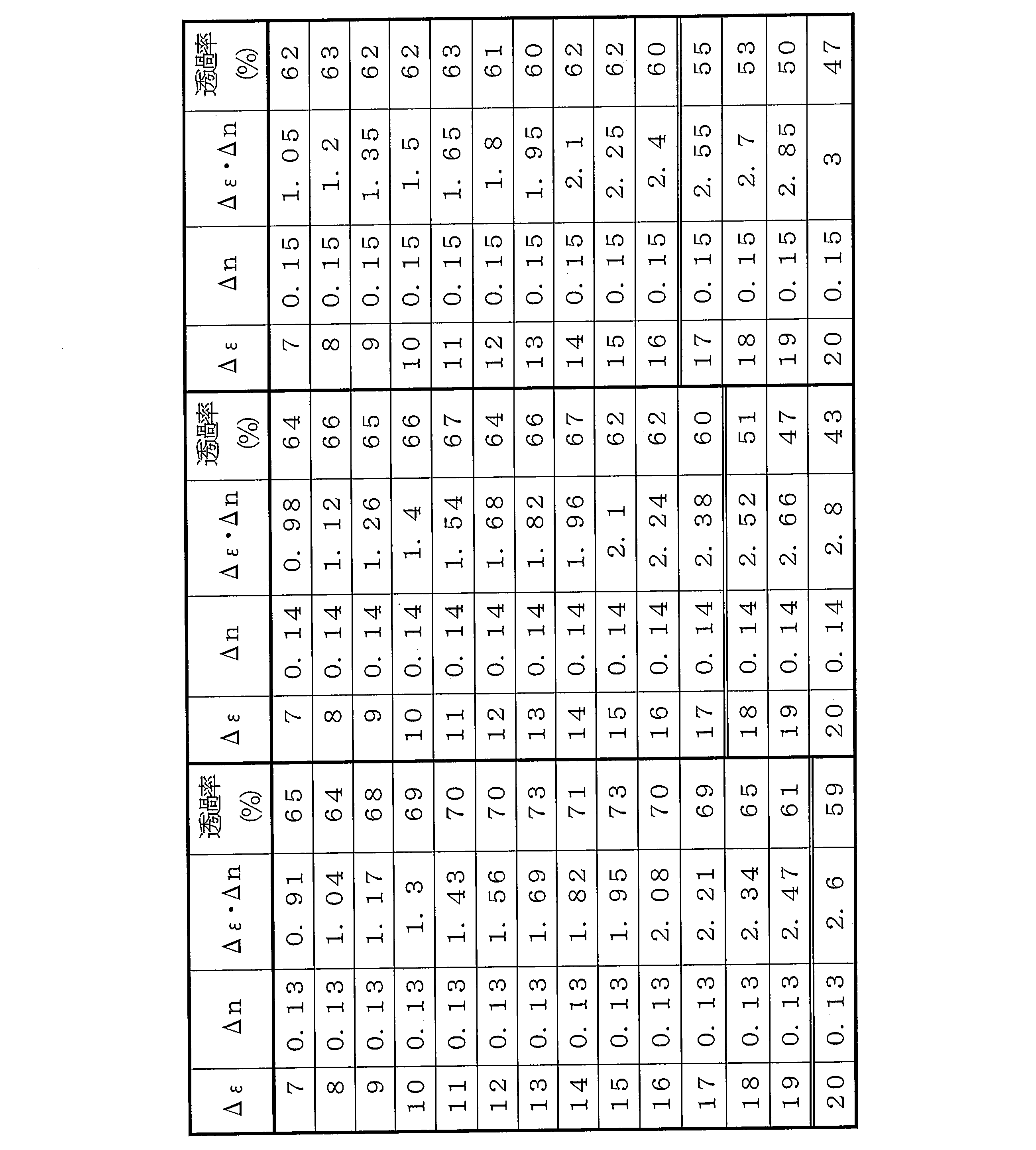
- Example 1 First, a solid electrode made of ITO was formed on the entire surface of the glass substrate 11 as a common electrode 14 on the glass substrate 11 by sputtering.
- a silicon nitride (SiNx) film having a relative dielectric constant ⁇ of 6.9 was formed as a dielectric layer 41 with a film thickness of 0.1 ⁇ m on the common electrode 14 by a sputtering method.
- the pixel electrode 13 and the common electrode 14 were both 100 nm in thickness.
- an orientation film coating material “JALS-204” (trade name, solid content 5 wt.%, ⁇ -butyrolactone solution) manufactured by JSR Co., Ltd. is spin-coated on the dielectric layer 41 so as to cover the pixel electrode 13. It was applied by the method. Then, the board
- the alignment film 22 was formed on the glass substrate 21 by the same process as the alignment film 12. Thereby, the substrate 20 was formed.
- resin beads “Micropearl SP2035” (trade name, manufactured by Sekisui Chemical Co., Ltd.) having a diameter of 3.5 ⁇ m were dispersed as spacers 33 on the substrate 40.
- a sealing resin “Struct Bond XN-21S” (trade name, manufactured by Mitsui Toatsu Chemical Co., Ltd.) was printed on the substrate 20 as the sealing agent 34.
- the substrates 10 and 20 were bonded to each other and baked at 135 ° C. for 1 hour, whereby a liquid crystal cell 5 was produced.
- liquid crystal layer 30 a p-type liquid crystal material having different dielectric anisotropy ⁇ and refractive index anisotropy ⁇ n as a liquid crystal material was sealed in the liquid crystal cell 5 by a vacuum injection method to form a liquid crystal layer 30.
- the polarizing plates 35 and 36 are placed on the front and back surfaces of the liquid crystal cell 5, the transmission axes of the polarizing plates 35 and 36 are orthogonal to each other, and the direction in which the pixel electrode 13 is extended and the transmission axes of the polarizing plates 35 and 36. Were pasted to form an angle of 45 °.
- 98 liquid crystal panels 2 liquid crystal display elements having the configuration shown in FIG. 1 were produced.
- each liquid crystal panel 2 when a voltage (rectangular wave) of 0 V to 20 V is applied between the common electrode 14 and each pixel electrode 13 at room temperature (25 ° C.).
- Tables 1 and 2 show the maximum transmittance.
- this mode has high speed, wide viewing angle, and high contrast, but has a problem of low transmittance.
- the transmittance is 60% or more as described above, it is not necessary to separately provide a brightness enhancement film, and the liquid crystal panel 2 in the above mode can be manufactured at low cost. Further, when the transmittance exceeds 70%, it becomes possible to suppress the power consumption of the backlight as compared with the current liquid crystal panel, and its practical value is extremely large.
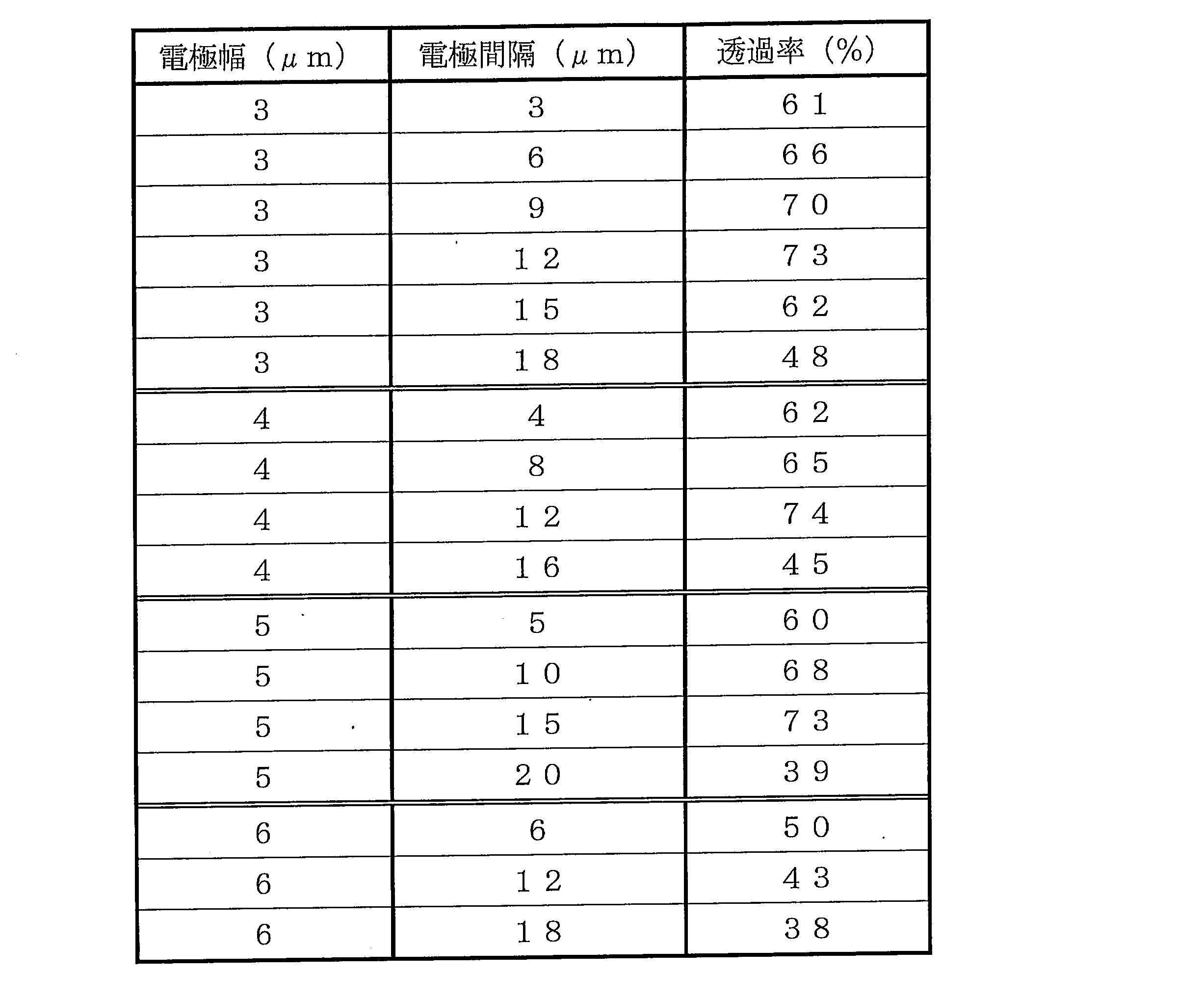
- Example 2 As described above, the degree of bend alignment depends on the physical properties of the liquid crystal material (product of dielectric anisotropy ⁇ and refractive index anisotropy ⁇ n), but the electrode width L and the electrode spacing S of the comb-like electrodes. It also changes depending on. Therefore, next, the electrode width L and the electrode interval S of the comb-like electrode suitable for this mode will be verified.
- each liquid crystal panel 2 when a voltage (rectangular wave) of 0 V to 20 V is applied between the common electrode 14 and each pixel electrode 13 at room temperature (25 ° C.).
- Table 3 shows the maximum transmittance.
- the transmitted light is modulated more greatly between the comb-shaped electrodes than on the comb-shaped electrodes. For this reason, in principle, it is preferable that the electrode interval S> the electrode width L.
- the transmittance gradually increases by widening the electrode interval S of the pixel electrode 13 which is a comb-like electrode, and when the electrode interval S exceeds 15 ⁇ m, the transmittance decreases rapidly. I understand. This is because the electric field strength becomes weaker as the electrode spacing S becomes larger, and thus the drive voltage becomes substantially higher.
- the results shown in Table 2 indicate that the electrode width L of the comb-like electrode is preferably 5 ⁇ m or less, and the electrode interval S is preferably 15 ⁇ m or less.
- this tendency is not limited to the liquid crystal panel 2 described above, but the liquid crystal panel 2 having the basic configuration shown in FIGS. It was found that it can be seen in common.
- liquid crystal panel 2 according to the present embodiment has a very simple configuration, and can be manufactured without major design changes. For this reason, the liquid crystal panel 2 can be manufactured at low cost.
- FIG. 10A is a cross-sectional view schematically showing a schematic configuration of the main part of the liquid crystal panel 2 according to the present embodiment, and FIG. 10B shows each electrode shown in FIG. It is a timing chart of the applied voltage in.
- the liquid crystal panel 2 includes a substrate 50 instead of the substrate 10 shown in FIGS. 3 and 4, and the substrate 20 shown in FIGS.
- the liquid crystal panel 2 has the same configuration as that of the liquid crystal panel 2 shown in FIGS. 3 and 4 except that a substrate 60 is provided instead.
- the liquid crystal cell 5 in the liquid crystal panel 2 has a configuration in which the substrate 50 and the substrate 60 are arranged to face each other with the liquid crystal layer 30 containing a p-type liquid crystal material interposed therebetween.
- the substrate 50 has a structure in which the pixel electrode 13 and the alignment film 12 are provided in this order on the glass substrate 11.
- the substrate 60 has a structure in which the common electrode 14 and the alignment film 22 are provided in this order on the glass substrate 21.
- the pixel electrode 13 is a comb-like electrode
- the common electrode 14 is a solid electrode.
- the common electrode 14 is formed on the glass substrate 21 over almost the entire surface of the glass substrate 21 so as to cover the display region (the region surrounded by the sealant 34) of the substrate 60.
- the alignment films 12 and 22 are provided so as to cover the pixel electrode 13 and the common electrode 14, respectively.
- the material of the pixel electrode 13 and the common electrode 14 is not particularly limited, and the same electrode material as the above exemplified electrode material can be used.
- the common electrode 14 is a transparent electrode material film such as ITO.
- the liquid crystal panel 2 shown in FIG. 10A has a configuration in which the common electrode 14 is provided on the substrate 60 facing the substrate 50 on which the pixel electrode 13 made of a comb-like electrode is provided. ing.
- the pixel electrode 13 formed of a comb-like electrode functions as an electric field applying unit that applies a lateral electric field to the liquid crystal layer 30.
- pixel electrode 13A and 13B two pixel electrodes 13 are arranged independently of each other. It is provided so that it can be driven.
- the pixel electrodes 13A and 13B provided so as to be driven independently from each other are provided with branch electrodes (branches) extending from the respective trunk electrodes (trunk lines). Lines) are alternately arranged so as to mesh with each other.
- the common electrode 14 so that the pixel electrode 13A (first pixel electrode) and the pixel electrode 13B (second pixel electrode) are always in opposite phases.
- a voltage is applied between the pixel electrodes 13A and 13B. Thereby, a lateral electric field can be applied to the liquid crystal layer 30.
- FIG. 11 shows the p-type liquid crystal molecules 31 in the liquid crystal cell 5 when a voltage (rectangular wave) of +6 V or ⁇ 6 V is applied to the pixel electrodes 13A and 13B shown in FIGS. A director distribution and an equipotential curve are shown. In addition, the equipotential curve was described at intervals of 0.5V.
- the lines of electric force work in the direction perpendicular to the equipotential curve.
- the electric lines of force at this time are shown in FIG. From FIG. 11, also in the present embodiment, a horizontal electric field is applied to the liquid crystal layer 30, and the electric field lines between the pixel electrode 13 and the common electrode 14 are curved in a semicircular shape due to the application of the electric field. It can be seen that the bend is arranged like a bow in the thickness direction of the substrate.
- liquid crystal panel 2 is used to further verify the optimum liquid crystal property values.
- JALS-204 trade name, solid content 5 wt.%, ⁇ -butyrolactone solution
- substrate 50 with which the alignment film 12 which is a vertical alignment film was provided on the glass substrate 11 so that the pixel electrode 13A and the pixel electrode 13B might be covered was formed by baking at 200 degreeC for 2 hours.
- the resulting alignment film 12 had a dry film thickness of 60 nm.
- an alignment film 22 having a dry film thickness of 60 nm is formed on a glass substrate 21 provided with a transparent electrode made of ITO having a thickness of 100 nm as a common electrode 14 on one main surface in the same process as the alignment film 12. Was deposited. Thereby, the substrate 60 was formed.
- resin beads “Micropearl SP2035” (trade name, manufactured by Sekisui Chemical Co., Ltd.) having a diameter of 3.5 ⁇ m were dispersed as spacers 33 on the substrate 50.
- a sealing resin “Struct Bond XN-21S” (trade name, manufactured by Mitsui Toatsu Chemical Co., Ltd.) was printed on the substrate 60 as the sealing agent 34.
- the substrates 50 and 60 were bonded together and baked at 135 ° C. for 1 hour, whereby a liquid crystal cell 5 was produced.
- liquid crystal panel 2 liquid crystal display elements
- Non-Patent Document 1 has a configuration similar to that of the liquid crystal panel 2 according to the present embodiment.
- Non-Patent Document 1 is not intended to improve the transmittance as in the present invention. Further, no attention is paid to the product of the dielectric anisotropy ⁇ and the refractive index anisotropy ⁇ n.
- the transmittance is also smaller than the current MVA mode.
- FIG. 12 is a cross-sectional view schematically showing a schematic configuration of a main part of the liquid crystal panel 2 according to the present embodiment.
- the liquid crystal panel 2 has the liquid crystal shown in FIGS. 3 and 4 except that it includes a substrate 70 instead of the substrate 20 shown in FIGS. It has the same configuration as the panel 2.
- the liquid crystal panel 2 shown in FIG. 12 includes a common electrode on each of a pair of opposing substrates 10 and 70.
- the substrate 10 is provided with a pair of comb-like electrodes as a pixel electrode 13 and a common electrode 14 (first common electrode) on a glass substrate 11.
- An alignment film 12 is provided so as to cover the electrode 14.
- the pixel electrode 13 and the common electrode 14 function as an electric field applying unit that applies a lateral electric field to the liquid crystal layer 30.
- the substrate 70 has a structure in which the common electrode 71 (second common electrode), the dielectric layer 72, and the alignment film 22 are provided in this order on the glass substrate 21.
- the common electrode 71 is a solid electrode, and is formed on the glass substrate 21 over almost the entire surface of the glass substrate 21 so as to cover the display region (the region surrounded by the sealant 34) of the substrate 70. ing.
- the dielectric layer 72 is provided so as to cover the common electrode 71.
- the alignment film 22 is provided so as to cover the dielectric layer 72.
- the thickness of the dielectric layer 72 is preferably about 1 ⁇ m to 3 ⁇ m from the viewpoint of processability.
- the range of dielectric constant ⁇ is 3 to 7 in order to efficiently rotate the liquid crystal near the substrate interface by electric field control.
- the dielectric layer 72 may be an organic dielectric layer such as an acrylic resin or an inorganic dielectric layer such as silicon nitride (SiNx).
- the material of the pixel electrode 13 and the common electrodes 14 and 71 is not particularly limited, and the same electrode material as the above exemplified electrode material can be used. As shown in FIG. 12, when the substrate 70 is used as the upper substrate, a transparent electrode material film such as ITO is used as the common electrode 71.
- liquid crystal panel 2 is used to verify the relationship between applied voltage, transmittance, and response time.
- an alignment film paint “JALS-204” (trade name, solid content 5 wt.%, ⁇ -butyrolactone solution) manufactured by JSR Co. was applied on the dielectric layer 72 by a spin coating method. Then, the board
- the same alignment film 12 as the alignment film 22 was formed in the same manner as the alignment film 22.
- the substrate 10 was formed.
- the thickness of the pixel electrode 13 and the common electrodes 14 and 71 was 100 nm.
- the potential of the common electrodes 14 and 71 is set to 0 V, and the potential of the pixel electrode 13 is changed between 0 to 8 V.
- the electro-optical characteristics at room temperature (25 ° C.) were measured. The results are shown in Table 5.
- the response time was defined as the time required for the transmittance to change by 90% when a predetermined voltage was applied from the state where no voltage was applied.
- the response time shown in Table 5 represents the sum of the rise response time and the fall response time.
- the response time of 16 ms means that a sufficient liquid crystal response can be realized within one frame, and its practical value is great.
- the common electrode 71, the dielectric layer 72, and the alignment film 22 are provided in this order on the glass substrate 21.
- the present embodiment is not limited to this.
- FIG. 13 shows the electric field distribution in the liquid crystal cell 5 when the voltage of 8 V is applied to the liquid crystal panel 2 produced in this Example 4 based on the material property values and the cell configuration used in this Example 4. The calculation result of the liquid crystal director distribution in the liquid crystal cell 5 is shown.
- the pixel electrode 13, the common electrodes 14 and 71, and the alignment films 12 and 22 are not shown.
- the common electrode 71 is formed on the substrate 70 opposite to the substrate 10 on which the comb-like electrodes are provided so that the electric lines of force can be deformed near the surface of the substrate 70 as described above. It is only necessary to be provided, and it is only necessary to be provided on at least one surface of the glass substrate 21 in the substrate 70.
- the substrate 70 is provided with the dielectric layer 41 and the alignment film 22 in this order on the surface of the glass substrate 21 facing the liquid crystal layer 30, and is opposite to the surface of the glass substrate 21 facing the liquid crystal layer 30.
- the present embodiment the case where comb-like electrodes (that is, the pixel electrode 13 and the common electrode 14) are provided in the same layer on the glass substrate 11 of one substrate 10 has been described as an example. .
- the present embodiment is not limited to this.
- the pixel electrode 13 and the common electrode 14 may be provided in different layers with a dielectric layer interposed therebetween. That is, for example, the substrate 10 is provided with a comb-like electrode as the common electrode 14 on the glass substrate 11, and the dielectric layer 41 is provided on the glass substrate 11 so as to cover the comb-like electrode. Further, a comb-like electrode may be provided as the pixel electrode 13, and the alignment film 12 may be provided on the dielectric layer 41 so as to cover the comb-like electrode.
- the pixel electrode 13 and the common electrode 14 are connected to each other through the dielectric layer 41 in a plan view (that is, when the substrate 10 is viewed from a direction perpendicular to the substrate). Are alternately arranged so that the branch electrodes are parallel to each other.
- a fringe electric field is generated between the pixel electrode 13 and the common electrode 14 by setting the electrode interval S between the pixel electrode 13 and the common electrode 14 to be shorter than the cell gap d.
- the pixel electrode 13 and the common electrode 14 provided on the same substrate are formed in different layers with a dielectric layer therebetween, thereby improving the yield compared to the case of providing the same layer. Can be made. Therefore, according to the present embodiment, the liquid crystal panel 2 that can simultaneously realize high-speed response, wide viewing angle characteristics, and high contrast characteristics, and the liquid crystal display device 1 including the liquid crystal panel 2 are inexpensive and stable. Can be produced.
- FIG. 14 is a plan view schematically showing a schematic configuration of one pixel of the electrode substrate used in the liquid crystal panel 2 according to the present embodiment
- FIG. 15 is an equivalent circuit of each electrode shown in the electrode substrate.
- one of the pixel electrodes 13 adjacent to each other is referred to as a “pixel electrode 13A” and the other is referred to as a “pixel electrode 13B”.
- the case where the pixel electrode 13 and the common electrode 14 are arranged in the layer direction similarly to the cross-sectional view shown in FIG. 1 will be described as an example.
- this embodiment refer to FIG. 1 for the cross-sectional configuration.
- this embodiment is not limited to this, and may have the configuration shown in FIG.
- the liquid crystal panel 2 includes a plurality of gate lines GL (gate lines GL (n) ⁇ GL (n + 1)... GL (n + m), m is an integer of 1 or more) And a plurality of data lines SLA (data lines SLA (n) .SLA (n + 1)... SLA (n + m), m represents an integer of 1 or more) and data lines SLB (data lines SLB (n) .SLB (n + 1) )... SLB (n + m), m represents an integer of 1 or more), respectively, are provided so as to intersect (orthogonally).
- the data lines SLA and the data lines SLB are alternately provided so as to be adjacent to each other in the column direction, for example.
- the column direction and the row direction can be interchanged.
- data line SLA and the data line SLB are collectively referred to, they are simply referred to as “data line SL”.
- the substrate 10 that is an electrode substrate is an active matrix type element substrate, and as shown in FIG. It has a configuration in which double the number of data lines SL are provided.
- the display unit is configured in units of pixels including the gate line GL and the data lines SLA / SLB.
- the liquid crystal panel 2 applies signal voltages generated from the signal electrodes in the data lines SLA and SLB to the pixel electrodes 13A and 13B that are comb-like electrode pairs, and the pixel electrodes 13A and 13B, the common electrode 14, and the like.
- the liquid crystal layer 30 is driven by an electric field formed between the two. As described above, in the liquid crystal panel 2, a potential difference is formed by providing two data lines SL in one pixel.
- two TFTs 81 and 82 are provided in one pixel of the liquid crystal panel 2, and two pixel electrodes 13 ⁇ / b> A provided as the pixel electrodes 13 so as to be driven independently of each other. -13B is provided.
- the TFT 81 is provided at the intersection of the gate line GL (n) and the data line SLA (n) and functions as a switching element for the pixel electrode 13A.
- the TFT 82 is provided at the intersection of the gate line GL (n) and the data line SLB (n) and functions as a switching element for the pixel electrode 13B.
- the pixel electrode 13 A is connected to the drain electrode of the TFT 81, and the pixel electrode 13 B is connected to the drain electrode of the TFT 82.
- different data lines SLA (n) and SLB (n) are connected to the source electrodes of the two TFTs 81 and 82, respectively. That is, the data line SLA (n) is connected to the source electrode of the TFT 81, and the data line SLB (n) is connected to the source electrode of the TFT 82.
- the gate electrodes of the TFTs 81 and 82 are connected to a common gate line GL (n). Accordingly, the TFTs 81 and 82 can drive the pixel electrodes 13A and 13B at the same timing.
- a capacitance line CL is formed between the gate line GL (n) and the adjacent gate line GL (n + 1) in parallel with the gate lines GL (n) ⁇ GL (n + 1).
- the pixel electrodes 13A and the pixel electrodes 13B each have a comb-like structure, and are arranged to alternately face each other so that branch electrodes extending from the trunk electrodes mesh with each other.
- a part of the branch electrode of the pixel electrode 13A is formed wider than the line width of the other branch electrode so as to shield the data line SLB (n) provided in the lower layer.
- the liquid crystal capacitors Clc1 and Clc2 and the storage capacitor Cst1 -Cst2 is formed respectively.
- the switching operation of the TFT 81 forms the liquid crystal capacitor Clc1 and the storage capacitor Cst2 that store charges by the voltage applied to the data line SLA (n).
- the liquid crystal capacitor Clc2 and the storage capacitor Cst2 that are applied to the data line SLB (n) and store charges by the voltage are formed.
- FIG. 16 is a timing chart of applied voltages applied to the pixel electrodes 13A and 13B, the gate lines GL (n) connected to the gate electrodes of the TFTs 81 and 82, and the common electrode 14.
- the substrate 10 (electrode substrate) having the above configuration can be suitably used for the liquid crystal panel 2 that requires a high applied voltage.
- a liquid crystal material having a relatively small dielectric anisotropy ⁇ can be used.
- a liquid crystal material having a relatively low viscosity can be used, and the response time can be reduced.
- a voltage twice as high as the signal voltage can be applied to the liquid crystal layer 30.
- a voltage twice the applied voltage can be applied between the pixel electrode 13A and the pixel electrode 13B. Therefore, since the driving voltage can be suppressed, it is not necessary to use a highly durable driver. For this reason, the liquid crystal panel 2 can be manufactured at low cost.
- the voltage actually applied to the pixel electrodes 13A and 13B can be reduced to 1 ⁇ 2 of the voltage applied to the liquid crystal layer 30, thereby reducing power consumption. You can also. Below, it demonstrates concretely using an Example.
- Example 5 the liquid crystal panel 2 shown in FIG. 14 was used to measure its electro-optical characteristics.
- the electrode interval S of the pixel electrode 13 (that is, the electrode interval between the pixel electrode 13A and the pixel electrode 13B) was 7.5 ⁇ m.
- the electrode width L of the pixel electrode 13 (that is, the electrode width of the pixel electrode 13A and the pixel electrode 13B) was 2.5 ⁇ m.
- ITO was used for the pixel electrode 13 and the common electrode 14, respectively, and the thickness thereof was 100 nm. Further, a color filter substrate having a color filter layer was used for the opposite substrate 20.
- the cell gap d liquid crystal layer thickness
- the polarizing plates 35 and 36 were bonded to the front and back surfaces of the liquid crystal cell 5 so that the respective transmission axes were orthogonal to each other.
- a voltage was applied to the pixel electrode 13A and the pixel electrode 13B through the TFTs 81 and 82 so that the amplitude was the same and the phase was always opposite.
- the transmittance at room temperature 25 ° C.
- the response time was 3.3 ms rise, 4.0 ms fall, and the contrast ratio was 3500: 1.
- the case where two data lines SL and two TFTs are provided in one pixel has been described as an example.
- the present embodiment is not limited to this.
- three data lines SL and three TFTs may be provided.
- the pixel electrodes 13A and 13B can be driven by independent signal voltages. High voltage driving can be performed without using a driver with high withstand voltage.
- the dielectric anisotropy ⁇ of the p-type liquid crystal material is obtained as described above.
- the refractive index anisotropy ⁇ n are preferably in the range of 0.9 to 2.5 as described above.
- the panel phase difference ⁇ nd is increased, the viewing angle characteristics are deteriorated. Therefore, practically, it is desirable to increase ⁇ within a range in which reliability is not lowered, rather than increasing ⁇ n. Therefore, according to the present invention, it is possible to improve transmittance and response speed while maintaining viewing angle characteristics and reliability.
- the voltage applied to the common electrodes 14 and 71 has been described as 0 V, but the present invention is not limited to this.
- the voltage applied to the pixel electrode and the common electrode is not particularly limited, and any voltage applied between the electrodes for applying a lateral electric field to the liquid crystal layer 30 is 7 V or higher. Combinations may be used.
- the comb-like electrode may be formed in a V shape or a zigzag shape regardless of the pixel electrode and the common electrode.
- the p-type liquid crystal material for example, a p-type nematic liquid crystal material can be used, but the present invention is not limited to this.
- the liquid crystal panel 2 and the liquid crystal display device 1 form a distribution of electric field strength in the liquid crystal cell 5 by applying an electric field, thereby realizing a bend alignment of the liquid crystal material.
- a liquid crystal material having a large refractive index anisotropy ⁇ n or a liquid crystal material having a large dielectric anisotropy ⁇ is preferably used.
- p-type liquid crystal materials include CN (cyano) liquid crystal materials (chiral nematic liquid crystal materials) and F (fluorine) liquid crystal materials.
- a liquid crystal panel includes a liquid crystal material sandwiched between a pair of substrates, and a plurality of electrodes including comb-like electrodes and applying an electric field parallel to the substrate surface to the liquid crystal material.
- the liquid crystal material includes a p-type liquid crystal material, and the p-type liquid crystal material is aligned perpendicular to the substrate surface when no electric field is applied.
- the liquid crystal panel has an electrode width of 5 ⁇ m or less and an electrode interval of 15 ⁇ m or less, and a voltage of 7 V or more is applied between electrodes for applying an electric field parallel to the substrate surface to the liquid crystal material during driving.
- the product ( ⁇ ⁇ ⁇ n) of the dielectric anisotropy ⁇ and the refractive index anisotropy ⁇ n of the p-type liquid crystal material is 0.9 or more and 2.5 or less.
- a liquid crystal panel for example, (I) a plurality of electrodes for applying an electric field parallel to the substrate surface to the liquid crystal material, a pixel electrode and a common electrode provided on one of the pair of substrates
- a liquid crystal panel in which at least the pixel electrode of the pixel electrode and the common electrode is a comb-like electrode.
- the liquid crystal panel described in (I) above has a very simple configuration and can be manufactured without major design changes. For this reason, the liquid crystal panel can be manufactured at low cost.
- a common electrode that covers the entire display region is further provided on the other of the pair of substrates.
- the lines of electric force near the other substrate are deformed by the common electrode provided on the other substrate.
- the p-type liquid crystal molecules in the vicinity of the other substrate are greatly inclined in the horizontal direction.
- the p-type liquid crystal molecules can be rotated even in the vicinity of the surface of the other substrate. For this reason, when the drive voltage is the same, the transmittance can be further improved as compared with the case where the common electrode is not provided on the other substrate.
- a plurality of electrodes for applying an electric field parallel to the substrate surface to the liquid crystal material includes the pair of electrodes. At least two pixel electrodes provided on one of the substrates, the pixel electrodes are composed of comb-like electrodes, and voltages having phases opposite to each other are applied between adjacent pixel electrodes during driving. In addition, there is a liquid crystal panel in which a common electrode is provided on at least one of the pair of substrates.
- the one substrate includes a plurality of data lines that are multiple times the gate line, and a switching element at each intersection of each data line and the gate line.
- the pixel electrodes adjacent to each other are connected to switching elements adjacent to each other along the gate line, and each pixel includes at least two switching elements adjacent to each other along the gate line and the switching It is preferable to include at least two pixel electrodes respectively connected to the element.
- the liquid crystal panel and the liquid crystal display device according to the present invention do not require an initial bend transition operation, have a high transmittance at a practical driving voltage, have a wide viewing angle characteristic equivalent to the MVA mode and the IPS mode, and the OCB. High-speed response comparable to or higher than the mode and high contrast characteristics can be realized at the same time. Therefore, it can be particularly suitably used for public bulletin boards for outdoor use, mobile devices such as mobile phones and PDAs.
Landscapes
- Physics & Mathematics (AREA)
- Chemical & Material Sciences (AREA)
- Crystallography & Structural Chemistry (AREA)
- Engineering & Computer Science (AREA)
- General Physics & Mathematics (AREA)
- Nonlinear Science (AREA)
- Computer Hardware Design (AREA)
- Theoretical Computer Science (AREA)
- Geometry (AREA)
- Mathematical Physics (AREA)
- Optics & Photonics (AREA)
- Liquid Crystal (AREA)
Abstract
Description
本発明の一実施形態について図1に基づいて説明すれば以下の通りである。
まず、ガラス基板11上に、共通電極14として、ITOからなるベタ状の電極を、スパッタ法にて上記ガラス基板11の表面全面に形成した。

前記したように、ベンド配列の程度は、液晶材料の物性(誘電率異方性Δεと屈折率異方性Δnとの積)に依存するが、櫛歯状電極の電極幅L、電極間隔Sによっても変化する。そこで、次に、本モードに適した櫛歯状電極の電極幅Lおよび電極間隔Sについて検証する。
本発明の他の実施形態について図10の(a)・(b)および図11に基づいて説明すれば以下の通りである。
まず、画素電極13として、電極幅L=3.0μm、電極間隔S=8.0μm、厚み=100nmのITO製の櫛歯状電極(互いに隣り合う画素電極13の一方を「画素電極13A」、他方を「画素電極13B」とする)が設けられたガラス基板11上に、JSR社製の配向膜塗料「JALS-204」(商品名、固形分5wt.%、γ-ブチロラクトン溶液)を、スピンコート法にて塗布した。その後、200℃にて2時間焼成することにより、ガラス基板11上に、画素電極13Aおよび画素電極13Bを覆うように垂直配向膜である配向膜12が設けられた基板50を形成した。得られた配向膜12の乾燥膜厚は60nmであった。
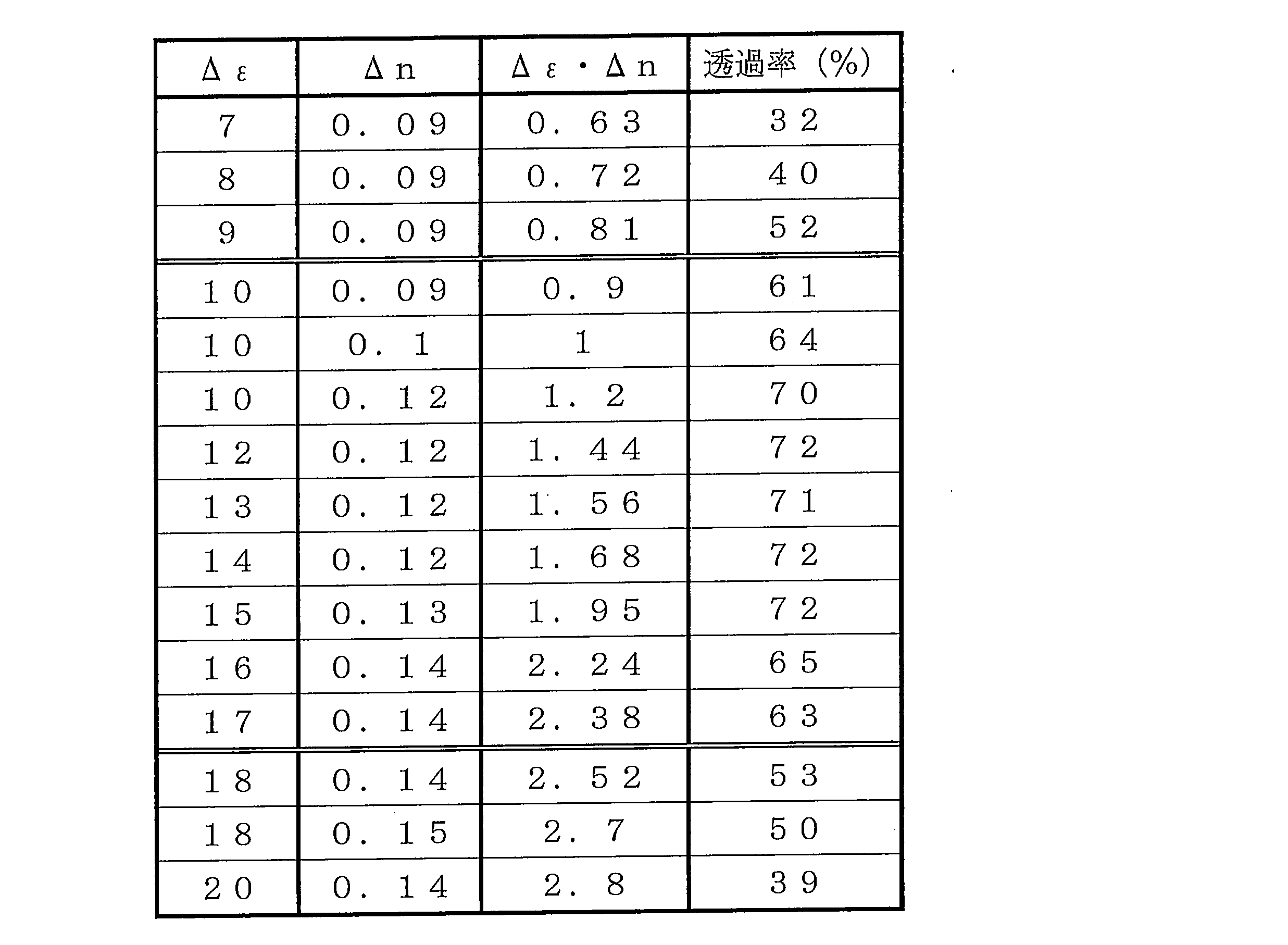
図12は、本実施の形態にかかる液晶パネル2の要部の概略構成を模式的に示す断面図である。
まず、一方の主面全体に、共通電極71としてITO製の透明な電極が設けられたガラス基板21上に、誘電率ε=3.7、膜厚3.2μmのアクリルレジストを成膜して、共通電極71を覆う誘電体層72を形成した。

本実施形態では、本発明のように高電圧駆動を行う場合に特に適した液晶パネル2について説明する。
本実施例では、図14に示す液晶パネル2を使用して、その電気光学特性を測定した。
2 液晶パネル
3 駆動回路
4 バックライト
5 液晶セル
10 基板
11 ガラス基板
12 配向膜
13 画素電極(電極)
13A 画素電極(電極)
13B 画素電極(電極)
14 共通電極(電極)
20 基板
21 ガラス基板
22 配向膜
30 液晶層
31 p型液晶分子
33 スペーサ
34 シール剤
35 偏光板
36 偏光板
37 位相差板
38 位相差板
40 基板
41 誘電体層
50 基板
60 基板
70 基板
71 共通電極(電極)
72 誘電体層
81 TFT(スイッチング素子)
82 TFT(スイッチング素子)
GL ゲートライン
SL データライン
SLA データライン
SLB データライン
CL 容量線
Claims (6)
- 一対の基板間に挟持された液晶材料と、櫛歯状電極を含み、基板面に平行な電界を上記液晶材料に印加する複数の電極とを備え、上記液晶材料はp型液晶材料を含み、電界無印加時に上記p型液晶材料が基板面に垂直に配向する液晶パネルにおいて、
上記櫛歯状電極の電極幅が5μm以下、電極間隔が15μm以下であり、
駆動時に、上記基板面に平行な電界を上記液晶材料に印加する電極間に7V以上の電圧が印加されるとともに、
上記p型液晶材料の誘電率異方性Δεと屈折率異方性Δnとの積が、0.9以上、2.5以下であることを特徴とする液晶パネル。 - 上記基板面に平行な電界を上記液晶材料に印加する複数の電極が、上記一対の基板のうち一方の基板に設けられた画素電極および共通電極であり、
上記画素電極および共通電極のうち少なくとも画素電極が櫛歯状電極からなることを特徴とする請求項1記載の液晶パネル。 - 上記一対の基板のうち他方の基板に、表示領域全域を覆う共通電極がさらに設けられていることを特徴とする請求項2記載の液晶パネル。
- 上記基板面に平行な電界を上記液晶材料に印加する複数の電極が、上記一対の基板のうち一方の基板に設けられた少なくとも2つの画素電極であり、
上記画素電極は櫛歯状電極からなり、互いに隣り合う画素電極間には、駆動時に互いに逆位相の電圧が印加されるとともに、
上記一対の基板のうち少なくとも一方の基板に共通電極が設けられていることを特徴とする請求項1記載の液晶パネル。 - 上記一方の基板は、ゲートライン1本に対し複数倍の本数のデータラインを備えるとともに、各データラインとゲートラインとの交差部毎にスイッチング素子が設けられており、
互いに隣り合う上記画素電極は、ゲートラインに沿って互いに隣り合うスイッチング素子に接続されており、
1画素に、ゲートラインに沿って互いに隣り合う少なくとも2つのスイッチング素子および該スイッチング素子にそれぞれ接続された少なくとも2つの画素電極を備えていることを特徴とする請求項4記載の液晶パネル。 - 請求項1~5の何れか1項に記載の液晶パネルを備えていることを特徴とする液晶表示装置。
Priority Applications (6)
| Application Number | Priority Date | Filing Date | Title |
|---|---|---|---|
| RU2011143858/28A RU2011143858A (ru) | 2009-05-29 | 2010-03-11 | Жидкокристаллическая панель и жидкокристаллическое дисплейное устройство |
| US13/257,414 US20120013594A1 (en) | 2009-05-29 | 2010-03-11 | Liquid crystal panel and liquid crystal display device |
| BRPI1011063A BRPI1011063A2 (pt) | 2009-05-29 | 2010-03-11 | painel de cristal líquido e dispositivo de exibição de cristal líquido |
| EP10780179.7A EP2437110A4 (en) | 2009-05-29 | 2010-03-11 | LIQUID CRYSTAL PANEL AND LIQUID CRYSTAL DISPLAY DEVICE |
| CN2010800191494A CN102414608A (zh) | 2009-05-29 | 2010-03-11 | 液晶面板和液晶显示装置 |
| JP2011515847A JPWO2010137217A1 (ja) | 2009-05-29 | 2010-03-11 | 液晶パネルおよび液晶表示装置 |
Applications Claiming Priority (2)
| Application Number | Priority Date | Filing Date | Title |
|---|---|---|---|
| JP2009131557 | 2009-05-29 | ||
| JP2009-131557 | 2009-05-29 |
Publications (1)
| Publication Number | Publication Date |
|---|---|
| WO2010137217A1 true WO2010137217A1 (ja) | 2010-12-02 |
Family
ID=43222350
Family Applications (1)
| Application Number | Title | Priority Date | Filing Date |
|---|---|---|---|
| PCT/JP2010/001756 Ceased WO2010137217A1 (ja) | 2009-05-29 | 2010-03-11 | 液晶パネルおよび液晶表示装置 |
Country Status (7)
| Country | Link |
|---|---|
| US (1) | US20120013594A1 (ja) |
| EP (1) | EP2437110A4 (ja) |
| JP (1) | JPWO2010137217A1 (ja) |
| CN (1) | CN102414608A (ja) |
| BR (1) | BRPI1011063A2 (ja) |
| RU (1) | RU2011143858A (ja) |
| WO (1) | WO2010137217A1 (ja) |
Cited By (5)
| Publication number | Priority date | Publication date | Assignee | Title |
|---|---|---|---|---|
| CN102629017A (zh) * | 2011-08-16 | 2012-08-08 | 京东方科技集团股份有限公司 | 一种液晶显示装置及其驱动方法 |
| CN102654694A (zh) * | 2011-09-06 | 2012-09-05 | 京东方科技集团股份有限公司 | 一种液晶显示面板及液晶显示器 |
| KR101413943B1 (ko) * | 2011-08-26 | 2014-07-01 | 보에 테크놀로지 그룹 컴퍼니 리미티드 | 호메오트로픽 배향 액정 디스플레이 및 그 제조방법 |
| US9454047B2 (en) | 2014-10-10 | 2016-09-27 | Shanghai Avic Optoelectronics Co., Ltd. | Liquid crystal display panel, method of driving the same and display device |
| US9964790B2 (en) | 2014-05-04 | 2018-05-08 | Boe Technology Group Co., Ltd. | Liquid crystal display panel and liquid crystal display device |
Families Citing this family (16)
| Publication number | Priority date | Publication date | Assignee | Title |
|---|---|---|---|---|
| TWI457875B (zh) * | 2009-02-19 | 2014-10-21 | Prime View Int Co Ltd | 顯示裝置及其製造方法 |
| KR20130049194A (ko) * | 2010-07-29 | 2013-05-13 | 도판 인사츠 가부시키가이샤 | 액정 표시 장치용 컬러 필터 기판 및 액정 표시 장치 |
| CN102866553B (zh) * | 2012-09-26 | 2016-01-20 | 南京中电熊猫液晶显示科技有限公司 | 一种金属氧化物平面开关型液晶显示面板的制造方法 |
| JP2014145992A (ja) * | 2013-01-30 | 2014-08-14 | Japan Display Inc | 液晶表示装置 |
| CN103676355A (zh) * | 2013-12-09 | 2014-03-26 | 京东方科技集团股份有限公司 | 阵列基板及其驱动方法、液晶显示面板、液晶显示装置 |
| KR20160050155A (ko) * | 2014-10-28 | 2016-05-11 | 삼성디스플레이 주식회사 | 액정 표시 장치 및 그 제조 방법 |
| CN104730783A (zh) * | 2015-04-10 | 2015-06-24 | 合肥京东方光电科技有限公司 | 一种阵列基板及其驱动方法和显示装置 |
| RU2625121C2 (ru) * | 2015-04-27 | 2017-07-11 | Государственное образовательное учреждение высшего образования Московской области Московский государственный областной университет | Способ получения гомеотропно ориентированного слоя жидкого кристалла жидкокристаллического устройства |
| CN105204232B (zh) * | 2015-10-14 | 2018-01-30 | 深圳市华星光电技术有限公司 | 液晶显示面板 |
| CN106154639B (zh) | 2016-09-29 | 2020-01-10 | 厦门天马微电子有限公司 | 一种液晶显示面板及液晶显示装置 |
| US10809529B2 (en) * | 2017-06-15 | 2020-10-20 | Microsoft Technology Licensing, Llc | Optical device having multiplexed electrodes |
| CN107272252A (zh) * | 2017-08-11 | 2017-10-20 | 京东方科技集团股份有限公司 | 显示面板及其制备方法、显示装置 |
| KR102803081B1 (ko) * | 2018-01-17 | 2025-05-07 | 세키스이가가쿠 고교가부시키가이샤 | 조광 적층체 및 조광 적층체용 수지 스페이서 |
| CN111081604A (zh) * | 2019-12-02 | 2020-04-28 | 深圳市华星光电半导体显示技术有限公司 | 微发光二极管转移装置及微发光二极管转移方法 |
| CN114185206B (zh) * | 2021-11-29 | 2022-08-26 | 绵阳惠科光电科技有限公司 | 防窥功能结构、显示面板及显示设备 |
| KR102907469B1 (ko) * | 2022-03-31 | 2026-01-05 | 삼성디스플레이 주식회사 | 표시 장치의 제조 장치 및 제조 방법 |
Citations (2)
| Publication number | Priority date | Publication date | Assignee | Title |
|---|---|---|---|---|
| JP2000081641A (ja) * | 1998-06-23 | 2000-03-21 | Fujitsu Ltd | 液晶表示装置 |
| JP2002139736A (ja) * | 2000-10-31 | 2002-05-17 | Sanyo Electric Co Ltd | 液晶表示装置 |
Family Cites Families (13)
| Publication number | Priority date | Publication date | Assignee | Title |
|---|---|---|---|---|
| US6704083B1 (en) * | 1997-05-30 | 2004-03-09 | Samsung Electronics, Co., Ltd. | Liquid crystal display including polarizing plate having polarizing directions neither parallel nor perpendicular to average alignment direction of molecules |
| TW434443B (en) * | 1997-05-30 | 2001-05-16 | Samsung Electronics Co Ltd | Liquid crystal display |
| WO1999032924A1 (fr) * | 1997-12-19 | 1999-07-01 | Hitachi, Ltd. | Afficheur a cristaux liquides |
| TW587191B (en) * | 1998-12-08 | 2004-05-11 | Fujitsu Display Tech | Liquid crystal display apparatus and liquid crystal display panel having wide transparent electrode and stripe electrodes |
| JP3634249B2 (ja) * | 1999-09-24 | 2005-03-30 | シャープ株式会社 | 液晶表示装置およびその表示方法 |
| JP4241238B2 (ja) * | 2003-08-29 | 2009-03-18 | 株式会社 日立ディスプレイズ | 液晶表示装置 |
| WO2005059637A1 (ja) * | 2003-12-18 | 2005-06-30 | Sharp Kabushiki Kaisha | 表示装置 |
| JP4477421B2 (ja) * | 2004-05-28 | 2010-06-09 | 富士通株式会社 | 液晶表示装置及びその製造方法 |
| JP4387276B2 (ja) * | 2004-09-24 | 2009-12-16 | シャープ株式会社 | 液晶表示装置 |
| KR101003623B1 (ko) * | 2004-12-31 | 2010-12-23 | 엘지디스플레이 주식회사 | 횡전계 모드 액정표시장치 |
| CN101055394B (zh) * | 2005-12-22 | 2010-10-13 | 日本电气液晶显示技术株式会社 | 液晶显示器件及使用其的终端器件 |
| JP2009047811A (ja) * | 2007-08-16 | 2009-03-05 | Epson Imaging Devices Corp | 液晶表示装置の製造方法及び液晶表示装置 |
| US8178173B1 (en) * | 2010-12-06 | 2012-05-15 | Sharp Kabushiki Kaisha | Liquid crystal display panel |
-
2010
- 2010-03-11 RU RU2011143858/28A patent/RU2011143858A/ru not_active Application Discontinuation
- 2010-03-11 JP JP2011515847A patent/JPWO2010137217A1/ja active Pending
- 2010-03-11 EP EP10780179.7A patent/EP2437110A4/en not_active Withdrawn
- 2010-03-11 WO PCT/JP2010/001756 patent/WO2010137217A1/ja not_active Ceased
- 2010-03-11 US US13/257,414 patent/US20120013594A1/en not_active Abandoned
- 2010-03-11 BR BRPI1011063A patent/BRPI1011063A2/pt not_active IP Right Cessation
- 2010-03-11 CN CN2010800191494A patent/CN102414608A/zh active Pending
Patent Citations (2)
| Publication number | Priority date | Publication date | Assignee | Title |
|---|---|---|---|---|
| JP2000081641A (ja) * | 1998-06-23 | 2000-03-21 | Fujitsu Ltd | 液晶表示装置 |
| JP2002139736A (ja) * | 2000-10-31 | 2002-05-17 | Sanyo Electric Co Ltd | 液晶表示装置 |
Non-Patent Citations (2)
| Title |
|---|
| See also references of EP2437110A4 |
| YOUNG CHO, SUNG MIN KIM, SEONG JIN HWANG, WOO II KIM, MI YOUNG KIM, JONG HO SON, JAE JIN RYU, KYEONG HYEON KIM, SEUNG HEE LEE: "New Vertical Alignment Liquid Crystal Device with Fast response Time and Small Color Shift", IDRC, no. 11.2, 2008, pages 246 - 248 |
Cited By (18)
| Publication number | Priority date | Publication date | Assignee | Title |
|---|---|---|---|---|
| CN102629017A (zh) * | 2011-08-16 | 2012-08-08 | 京东方科技集团股份有限公司 | 一种液晶显示装置及其驱动方法 |
| US9575342B2 (en) | 2011-08-16 | 2017-02-21 | Boe Technology Group Co., Ltd. | Liquid crystal display device comprising two different pixel electrodes connected to different TFTS in a pixel |
| WO2013023579A1 (zh) * | 2011-08-16 | 2013-02-21 | 京东方科技集团股份有限公司 | 液晶显示装置及液晶显示装置驱动方法 |
| JP2014529095A (ja) * | 2011-08-16 | 2014-10-30 | 京東方科技集團股▲ふん▼有限公司 | 液晶表示装置及び液晶表示装置駆動方法 |
| US20130148047A1 (en) * | 2011-08-16 | 2013-06-13 | Boe Technology Group Co., Ltd. | Liquid crystal display device and method for driving a liquid crystal display device |
| JP2014527201A (ja) * | 2011-08-26 | 2014-10-09 | 京東方科技集團股▲ふん▼有限公司 | 垂直配向型液晶ディスプレイ及びその製造方法 |
| KR101413943B1 (ko) * | 2011-08-26 | 2014-07-01 | 보에 테크놀로지 그룹 컴퍼니 리미티드 | 호메오트로픽 배향 액정 디스플레이 및 그 제조방법 |
| KR101431676B1 (ko) * | 2011-09-06 | 2014-08-20 | 보에 테크놀로지 그룹 컴퍼니 리미티드 | 액정 디스플레이 패널 및 액정 디스플레이 |
| KR101431164B1 (ko) * | 2011-09-06 | 2014-08-18 | 보에 테크놀로지 그룹 컴퍼니 리미티드 | 액정 디스플레이 패널 및 액정 디스플레이 |
| CN102654694B (zh) * | 2011-09-06 | 2014-03-26 | 京东方科技集团股份有限公司 | 一种液晶显示面板及液晶显示器 |
| JP2014528094A (ja) * | 2011-09-06 | 2014-10-23 | 京東方科技集團股▲ふん▼有限公司 | 液晶表示パネル及び液晶ディスプレイ |
| WO2013034077A1 (zh) * | 2011-09-06 | 2013-03-14 | 京东方科技集团股份有限公司 | 液晶显示面板及液晶显示器 |
| US8902387B2 (en) | 2011-09-06 | 2014-12-02 | Boe Technology Group Co., Ltd. | Liquid crystal display panel and liquid crystal display |
| EP2755081A4 (en) * | 2011-09-06 | 2015-05-06 | Boe Technology Group Co Ltd | Liquid crystal display panel and liquid crystal display device |
| US9097937B2 (en) | 2011-09-06 | 2015-08-04 | Boe Technology Group Co., Ltd. | Liquid crystal display panel and liquid crystal display |
| CN102654694A (zh) * | 2011-09-06 | 2012-09-05 | 京东方科技集团股份有限公司 | 一种液晶显示面板及液晶显示器 |
| US9964790B2 (en) | 2014-05-04 | 2018-05-08 | Boe Technology Group Co., Ltd. | Liquid crystal display panel and liquid crystal display device |
| US9454047B2 (en) | 2014-10-10 | 2016-09-27 | Shanghai Avic Optoelectronics Co., Ltd. | Liquid crystal display panel, method of driving the same and display device |
Also Published As
| Publication number | Publication date |
|---|---|
| EP2437110A1 (en) | 2012-04-04 |
| RU2011143858A (ru) | 2013-07-10 |
| US20120013594A1 (en) | 2012-01-19 |
| CN102414608A (zh) | 2012-04-11 |
| JPWO2010137217A1 (ja) | 2012-11-12 |
| EP2437110A4 (en) | 2014-01-01 |
| BRPI1011063A2 (pt) | 2016-04-05 |
Similar Documents
| Publication | Publication Date | Title |
|---|---|---|
| JPWO2010137217A1 (ja) | 液晶パネルおよび液晶表示装置 | |
| JP5068886B2 (ja) | 液晶パネルおよび液晶表示装置 | |
| CN102317849B (zh) | 液晶显示装置 | |
| CN101726953B (zh) | 液晶显示装置 | |
| TWI390291B (zh) | 液晶顯示裝置 | |
| US9494832B2 (en) | Liquid crystal display device | |
| EP2312385B1 (en) | Liquid crystal panel and liquid crystal display device | |
| JPH086025A (ja) | 液晶電気光学装置、それを用いた投射型表示システムおよび液晶電気光学装置の駆動方法 | |
| US9791746B2 (en) | Liquid crystal display panel | |
| JP4621788B2 (ja) | 液晶パネルおよび液晶表示装置 | |
| JP5335907B2 (ja) | 液晶パネルおよびその製造方法並びに液晶表示装置 | |
| WO2012017931A1 (ja) | 液晶パネルおよび液晶表示装置 | |
| US8199299B2 (en) | Liquid crystal panel, liquid crystal display device, and display method of liquid crystal panel | |
| WO2012086666A1 (ja) | 液晶パネルおよび液晶表示装置 | |
| CN113631997B (zh) | 液晶面板及显示装置 | |
| JP5273368B2 (ja) | 液晶表示装置 | |
| EP2461207B1 (en) | Liquid crystal panel and liquid crystal display device | |
| WO2010137213A1 (ja) | 液晶表示素子、及び、液晶表示装置 | |
| US20130148066A1 (en) | Liquid crystal panel and liquid crystal display device | |
| WO2009154258A1 (ja) | 液晶パネルおよび液晶表示装置 | |
| US20130329177A1 (en) | Liquid-crystal display | |
| KR20130084623A (ko) | 액정소자 및 그 구동방법 | |
| CN101592825A (zh) | 一种液晶显示器及实现液晶显示器高路数显示的方法 |
Legal Events
| Date | Code | Title | Description |
|---|---|---|---|
| WWE | Wipo information: entry into national phase |
Ref document number: 201080019149.4 Country of ref document: CN |
|
| 121 | Ep: the epo has been informed by wipo that ep was designated in this application |
Ref document number: 10780179 Country of ref document: EP Kind code of ref document: A1 |
|
| ENP | Entry into the national phase |
Ref document number: 2011515847 Country of ref document: JP Kind code of ref document: A |
|
| WWE | Wipo information: entry into national phase |
Ref document number: 13257414 Country of ref document: US |
|
| WWE | Wipo information: entry into national phase |
Ref document number: 8047/CHENP/2011 Country of ref document: IN |
|
| WWE | Wipo information: entry into national phase |
Ref document number: 2010780179 Country of ref document: EP |
|
| NENP | Non-entry into the national phase |
Ref country code: DE |
|
| ENP | Entry into the national phase |
Ref document number: 2011143858 Country of ref document: RU Kind code of ref document: A |
|
| REG | Reference to national code |
Ref country code: BR Ref legal event code: B01A Ref document number: PI1011063 Country of ref document: BR |
|
| ENP | Entry into the national phase |
Ref document number: PI1011063 Country of ref document: BR Kind code of ref document: A2 Effective date: 20111121 |