WO2010137427A1 - 液晶表示装置 - Google Patents
液晶表示装置 Download PDFInfo
- Publication number
- WO2010137427A1 WO2010137427A1 PCT/JP2010/057006 JP2010057006W WO2010137427A1 WO 2010137427 A1 WO2010137427 A1 WO 2010137427A1 JP 2010057006 W JP2010057006 W JP 2010057006W WO 2010137427 A1 WO2010137427 A1 WO 2010137427A1
- Authority
- WO
- WIPO (PCT)
- Prior art keywords
- liquid crystal
- display device
- crystal display
- electrode
- pair
- Prior art date
- Legal status (The legal status is an assumption and is not a legal conclusion. Google has not performed a legal analysis and makes no representation as to the accuracy of the status listed.)
- Ceased
Links
Images













Classifications
-
- G—PHYSICS
- G02—OPTICS
- G02F—OPTICAL DEVICES OR ARRANGEMENTS FOR THE CONTROL OF LIGHT BY MODIFICATION OF THE OPTICAL PROPERTIES OF THE MEDIA OF THE ELEMENTS INVOLVED THEREIN; NON-LINEAR OPTICS; FREQUENCY-CHANGING OF LIGHT; OPTICAL LOGIC ELEMENTS; OPTICAL ANALOGUE/DIGITAL CONVERTERS
- G02F1/00—Devices or arrangements for the control of the intensity, colour, phase, polarisation or direction of light arriving from an independent light source, e.g. switching, gating or modulating; Non-linear optics
- G02F1/01—Devices or arrangements for the control of the intensity, colour, phase, polarisation or direction of light arriving from an independent light source, e.g. switching, gating or modulating; Non-linear optics for the control of the intensity, phase, polarisation or colour
- G02F1/13—Devices or arrangements for the control of the intensity, colour, phase, polarisation or direction of light arriving from an independent light source, e.g. switching, gating or modulating; Non-linear optics for the control of the intensity, phase, polarisation or colour based on liquid crystals, e.g. single liquid crystal display cells
- G02F1/133—Constructional arrangements; Operation of liquid crystal cells; Circuit arrangements
- G02F1/1333—Constructional arrangements; Manufacturing methods
- G02F1/1343—Electrodes
- G02F1/134309—Electrodes characterised by their geometrical arrangement
- G02F1/134363—Electrodes characterised by their geometrical arrangement for applying an electric field parallel to the substrate, i.e. in-plane switching [IPS]
-
- G—PHYSICS
- G02—OPTICS
- G02F—OPTICAL DEVICES OR ARRANGEMENTS FOR THE CONTROL OF LIGHT BY MODIFICATION OF THE OPTICAL PROPERTIES OF THE MEDIA OF THE ELEMENTS INVOLVED THEREIN; NON-LINEAR OPTICS; FREQUENCY-CHANGING OF LIGHT; OPTICAL LOGIC ELEMENTS; OPTICAL ANALOGUE/DIGITAL CONVERTERS
- G02F1/00—Devices or arrangements for the control of the intensity, colour, phase, polarisation or direction of light arriving from an independent light source, e.g. switching, gating or modulating; Non-linear optics
- G02F1/01—Devices or arrangements for the control of the intensity, colour, phase, polarisation or direction of light arriving from an independent light source, e.g. switching, gating or modulating; Non-linear optics for the control of the intensity, phase, polarisation or colour
- G02F1/13—Devices or arrangements for the control of the intensity, colour, phase, polarisation or direction of light arriving from an independent light source, e.g. switching, gating or modulating; Non-linear optics for the control of the intensity, phase, polarisation or colour based on liquid crystals, e.g. single liquid crystal display cells
- G02F1/133—Constructional arrangements; Operation of liquid crystal cells; Circuit arrangements
- G02F1/1333—Constructional arrangements; Manufacturing methods
- G02F1/1343—Electrodes
- G02F1/134309—Electrodes characterised by their geometrical arrangement
- G02F1/134318—Electrodes characterised by their geometrical arrangement having a patterned common electrode
Definitions
- the present invention relates to a liquid crystal display device. More specifically, the present invention relates to a liquid crystal display device suitable for a vertical alignment mode having at least a pair of comb-like electrodes, such as a transverse bend alignment (TBA) mode.
- TSA transverse bend alignment
- a liquid crystal display device is a display device with low power consumption, and can be reduced in weight and thickness. Therefore, the liquid crystal display device is widely used for monitors for televisions, personal computers, and the like.
- VA mode vertical alignment
- the liquid crystal molecules are aligned substantially perpendicular to the substrate.
- the voltage between the substrates is sufficiently higher than the threshold voltage, the liquid crystal molecules are relative to the substrate. Oriented almost horizontally.
- an alignment division technique for dividing the tilt direction of liquid crystal molecules into two or more regions in a pixel has been developed. According to this, when a voltage is applied to the liquid crystal layer, the liquid crystal molecules are inclined in different directions within the pixel, so that the viewing angle characteristics of the liquid crystal display device can be improved.
- region from which the inclination direction of a liquid crystal molecule differs is also called a domain, and orientation division
- segmentation is also called a multi domain.
- the slit is opened in ITO (Indium Tin Oxide) which is a transparent electrode.
- ITO Indium Tin Oxide
- Such a liquid crystal display device is generally known as an MVA (Multi-Domain Vertical Alignment), ASV (Advanced Super View), or PVA (Patterned Vertical Alignment) mode and is in practical use.
- MVA Multi-Domain Vertical Alignment
- ASV Advanced Super View
- PVA Powerned Vertical Alignment
- the manufacturing process is complicated and there is room for improvement in that the response is slow as in the TN (Twisted Nematic) mode.
- the pixel electrode is divided into a plurality of subpixel electrodes, and at least some of the subpixel electrodes are connected to the switching element.
- a liquid crystal display device that is capacitively coupled to each other for example, see Patent Document 1.
- a matrix is formed on the substrate.
- a plurality of pixels each having a plurality of subpixel electrodes, a plurality of switching elements respectively connected to the plurality of subpixel electrodes, a plurality of data bus lines connected to the switching elements, and connected to the switching elements
- a plurality of gate bus lines for controlling the switching element; a data bus driving circuit for supplying a driving signal to the data bus line and applying the driving signal to the sub-pixel electrode through the switching element;
- an alignment regulating means for regulating the alignment direction of the liquid crystal molecules in a plurality of directions.
- the sub-pixel electrode is provided, and the data bus driving circuit generates a first driving signal for changing from a low luminance to a high luminance in accordance with an increase in gradation with respect to an input gradation of the image signal.
- the second drive signal applied to the electrode is changed from low luminance to high luminance in accordance with an increase in gradation with respect to the input gradation of the image signal, and a second drive signal having a lower brightness than the first drive signal is applied to the second
- a liquid crystal display device that is applied to a sub-pixel electrode is disclosed (see, for example, Patent Document 2).
- a liquid crystal layer is sealed between a pair of substrates, and a drive voltage is applied to two electrodes formed on the same substrate or both substrates, so that the substrate interface is almost
- a method of driving a liquid crystal layer with an electric field in a parallel direction and modulating and displaying light incident on the liquid crystal layer through a gap between two electrodes (hereinafter also referred to as a horizontal electric field method) is known.
- IPS In-plane Switching
- TBA Transverse Bend Alignment
- the liquid crystal layer is driven by a lateral electric field generated by a pixel electrode connected to an active element such as a TFT and a common electrode that is an electrode common to each pixel.
- an IPS mode liquid crystal display device for example, a pair of substrates, at least two display electrodes formed on one substrate of the pair of substrates so as to be insulated from each other, and so that the display electrodes are on the inside
- the liquid crystal material includes liquid crystal molecules having a twist direction opposite to the twist direction of the liquid crystal molecules when a potential difference is provided between the display electrodes.
- a liquid crystal display device is disclosed (for example, see Patent Document 3).
- the TBA mode is a display method in which p-type nematic liquid crystal is used as a liquid crystal material, and the liquid crystal molecules are driven by a horizontal electric field while maintaining high contrast by vertical alignment, thereby defining the orientation direction of liquid crystal molecules. Since this method does not require alignment control by protrusions, the pixel configuration is simple and it has excellent viewing angle characteristics.
- JP-A-2005-292397 JP 2005-316211 A Japanese Unexamined Patent Publication No. 7-92504
- Display modes such as the MVA mode, the PVA mode, and the TBA mode are normally normally black modes in which nematic liquid crystals are vertically aligned when no voltage is applied under the crossed Nicols setting.
- these modes have a so-called multi-domain (in-cell self-compensation) structure in which liquid crystal molecules are symmetrically tilted about the front direction when a voltage is applied in order to widen a viewing angle when a voltage is applied.
- the shape of the voltage-transmittance characteristic differs between the front direction and the oblique direction.
- This problem is particularly noticeable in gradations close to black display (low gradations), and the VT characteristics greatly depend on changes in polar angles at low gradations.
- a phenomenon occurs in which the dark display on the low gradation side floats white (becomes white). This phenomenon is also called whitening.
- this white floating phenomenon is not visually recognized in black and white display.
- the black and white display means that black and white display is performed by adjusting the brightness of a plurality of color picture elements (usually R (red), G (green), and B (blue) picture elements). To do.
- the mode of white floating will be described in more detail.
- the mode in which the nematic liquid crystal is vertically aligned when no voltage is applied including the TBA mode
- the liquid crystal molecules are tilted by applying a voltage
- the liquid crystal molecules are separated in the front direction and the diagonal direction.
- the liquid crystal molecules 4 appear circular from the front direction as shown in FIG. 11B.
- the polar angle in the observation direction is increased, the liquid crystal molecules 4 are observed in an elliptical shape (rod shape) as shown in FIG.
- the observation of the liquid crystal molecules 4 in a circular shape corresponds to the image being displayed in black, and the observation of the liquid crystal molecules 4 in an elliptical shape corresponds to the image becoming brighter. That is, even when the low gradation display is performed, if the polar angle in the observation direction is increased, light leaks (floats white).
- Patent Documents 1 and 2 describe techniques related to improvement of whitening in the MVA mode, but there is no description about the TBA mode.
- Patent Document 3 describes a technique for improving coloring in the IPS mode, but there is no description regarding improvement of whitening in the TBA mode.
- the subpixel electrode that exhibits a high threshold VT characteristic is controlled by a floating potential. For this reason, the charge once written to the electrode is difficult to escape, and the potential change of the pixel is slowed down. As a result, the display may be burned.
- the present invention has been made in view of the above situation, and an object of the present invention is to provide a liquid crystal display device capable of improving the white floating phenomenon in the vertical alignment mode having at least a pair of comb-like electrodes. is there.
- the present inventors have made various studies on a liquid crystal display device capable of improving the white floating phenomenon in the vertical alignment mode having at least a pair of comb-like electrodes such as the TBA mode.
- the distance between the pair of comb-like electrodes Attention was paid to the electrode spacing S.
- the thresholds of the VT characteristics in the two regions are made different, and the slope of the VT characteristics particularly in the low gradation is made smooth.
- the change in the VT characteristics depending on the polar angle in the observation direction can be reduced particularly on the low gradation side, and the inventors have conceived that the above problems can be solved brilliantly, thereby reaching the present invention. It is a thing.
- the present invention is a liquid crystal display device including a pair of substrates disposed to face each other and a liquid crystal layer sandwiched between the pair of substrates, wherein one of the pair of substrates is a pair of comb teeth.
- the pair of electrodes are arranged to face each other in a plane in the pixel, and the liquid crystal layer includes p-type nematic liquid crystal and is driven by an electric field generated between the pair of electrodes.
- the type nematic liquid crystal is aligned perpendicularly to the pair of substrate surfaces when no voltage is applied, and the liquid crystal display device includes a liquid crystal display having two or more regions in the pixel in which the distance between the pair of electrodes is different from each other. Device.
- the p-type nematic liquid crystal may exhibit an orientation sufficient to allow the liquid crystal display device of the present invention to function as a TBA mode liquid crystal display device when no voltage is applied.
- the configuration of the liquid crystal display device of the present invention is not particularly limited by other components as long as such components are essential. A preferred embodiment of the liquid crystal display device of the present invention will be described in detail below.
- the liquid crystal display device has the two different regions interval, the area towards the gap is narrow among the two regions as A n, towards the wider the interval of the two areas
- the liquid crystal display device preferably satisfies the a n ⁇ a w.
- the liquid crystal display device of the present invention may be a color liquid crystal display device, and the pixels may be picture elements (sub-pixels).
- liquid crystal display device of the present invention it is possible to improve the whitening phenomenon in the vertical alignment mode having at least a pair of comb-like electrodes.
- FIG. 3 is a schematic diagram showing VT characteristics of the liquid crystal display device of Embodiment 1.
- 3 is a schematic diagram showing VT characteristics of the liquid crystal display device of Embodiment 1.
- 3 shows an equivalent circuit in a picture element portion of the liquid crystal display device of Embodiment 1.
- It is a schematic diagram which shows the liquid crystal display device of the comparative form 1, (a) is sectional drawing, (b) is a top view. It is a figure which shows the electric lines of force and a liquid crystal director when it sees from the cross-sectional direction of the liquid crystal display device of the comparative form 1 calculated
- It is a plane schematic diagram which shows the structure of the pixel used for simulation (3D simulation). 6 is a graph showing VT characteristics of the liquid crystal display device of Embodiment 1.
- the white floating characteristic of a commercially available MVA mode television is shown.
- the white floating characteristic of the liquid crystal display device of the comparative form 1 is shown.
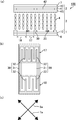
- 1 is a schematic plan view showing a liquid crystal display device of Embodiment 1.
- FIG. 1 is a schematic plan view showing a liquid crystal display device of Embodiment 1.
- FIG. 1 is a schematic plan view showing a liquid crystal display device of Embodiment 1.
- FIG. 1 is a schematic plan view showing a liquid crystal display device of Embodiment 1.
- FIG. 1 is a schematic plan view showing a liquid crystal display device of Embodiment 1.
- FIG. 1 is a schematic plan view showing a liquid crystal display device of Embodiment 1.
- FIG. 1 is a schematic plan view showing a liquid crystal display device of Embodiment 1.
- FIG. 1 is a schematic plan view showing a liquid crystal display device of Embodiment 1.
- FIG. It is a plane schematic diagram which shows the liquid crystal display device of the comparative form 2.
- It is a plane schematic diagram which shows the liquid crystal display device of the comparative form 2.
- It is a plane schematic diagram which shows the liquid crystal display device of the comparative form 2.
- FIG. 6 is a schematic cross-sectional view illustrating a configuration of a liquid crystal display device of Embodiment 2.
- FIG. 3 is a schematic plan view illustrating a configuration of a liquid crystal display device according to Embodiment 1 or 2.
- the 3 o'clock direction, the 12 o'clock direction, the 9 o'clock direction, and the 6 o'clock direction when the liquid crystal display panel (a pair of substrate surfaces) is viewed from the front is the 0 ° direction (azimuth), respectively.
- the 90 ° direction (azimuth), 180 ° direction (azimuth), and 270 ° direction (azimuth) are defined as the direction passing through 3 o'clock and 9 o'clock as the left-right direction, and the direction passing through 12 o'clock and 6 o'clock as the up-down direction.
- the front direction means a normal direction with respect to the display surface of the liquid crystal display panel.
- the polar angle means an angle formed with the normal direction to the display surface of the liquid crystal display panel.
- the oblique direction means a direction in which the polar angle exceeds 0 °.
- the liquid crystal display device applies an electric field (lateral electric field) in the substrate surface direction (direction parallel to the substrate surface) to the liquid crystal layer, and controls the orientation of the liquid crystal to perform image display.
- This is a transmissive liquid crystal display device adopting a method called a TBA method (TBA mode) among electric field methods.
- one picture element is mainly shown. However, in the display area (image display area) of the liquid crystal display device of this embodiment, a plurality of picture elements (sub-pixels) are arranged in a matrix. Is provided.
- the liquid crystal display device includes a liquid crystal display panel 100.
- the liquid crystal display panel 100 includes an active matrix substrate (array substrate) 1 and a pair of substrates arranged to face each other. It has a counter substrate 2 and a liquid crystal layer 3 sandwiched between them.
- a pair of linearly polarizing plates 6 and 7 are provided on the outer main surface of the array substrate 1 and the counter substrate 2 (on the side opposite to the liquid crystal layer 3).
- the absorption axis 6a of the linearly polarizing plate 6 on the array substrate 1 side is arranged in the 45 ° direction
- the absorption axis 7a of the linearly polarizing plate 7 on the counter substrate 2 side is in the 135 ° direction. Is arranged.
- the linearly polarizing plates 6 and 7 are arranged in crossed Nicols.
- both absorption axes 6 a and 7 a have an angle of 45 ° with respect to the extending direction of a branch portion 22 of the pixel electrode 20 and a branch portion 32 of the common electrode 30 described later.
- the array substrate 1 and the counter substrate 2 are bonded to each other with a sealant provided so as to surround the display area via a spacer such as plastic beads.
- a liquid crystal layer 3 is formed in the gap between the array substrate 1 and the counter substrate 2 by sealing a liquid crystal material as a display medium constituting the optical modulation layer.
- the liquid crystal layer 3 includes a nematic liquid crystal material (p-type nematic liquid crystal material) having positive dielectric anisotropy.
- the liquid crystal molecules 4 of the p-type nematic liquid crystal material are applied when no voltage is applied (the pixel electrode 20 and the common electrode described later) due to the alignment regulating force of the vertical alignment film provided on the surfaces of the array substrate 1 and the counter substrate 2 on the liquid crystal layer 3 side. Homeotropic alignment is exhibited when no electric field is generated between the electrodes 30). More specifically, the major axis of the liquid crystal molecules 4 has an angle of 88 ° or more (more preferably 89 ° or more) with respect to each of the array substrate 1 and the counter substrate 2 when no voltage is applied.
- the panel retardation d ⁇ n (product of the cell gap d and the birefringence ⁇ n of the liquid crystal material) is preferably 275 to 460 nm, and more preferably 280 to 400 nm.
- the lower limit of d ⁇ n is preferably at least a half wavelength of green 550 nm in terms of modes
- the upper limit of d ⁇ n is within a range that can be compensated by the retardation Rth in the normal direction of the negative C plate (single layer). It is preferable that The negative C plate is provided to compensate for whitening that occurs when observed from an oblique direction during black display. It is conceivable to accumulate Rth by laminating a negative C plate, but this is not preferable because of high cost.
- the dielectric constant ⁇ of the liquid crystal material is preferably 10 to 25, and more preferably 15 to 25.
- the lower limit of ⁇ is preferably about 10 (more preferably 15) or more because the white voltage (the voltage during white display) becomes high. The larger the ⁇ , the lower the applied voltage. This is preferable because it is possible.
- the upper limit of ⁇ is preferably 25 or less as described above.
- the counter substrate 2 has a black matrix (BM) layer 41 that shields light between the pixels on one main surface (on the liquid crystal layer 3 side) of the colorless and transparent insulating substrate 40, and a plurality of pixels provided in each pixel.
- Color layer (color filter) 42 an overcoat layer 43 covering the BM layer 41 and the color layer 42, and a vertical alignment film provided on the surface on the liquid crystal layer 3 side so as to cover these components.
- the BM layer 41 is formed of an opaque metal such as Cr, an opaque organic film such as an acrylic resin containing carbon, or the like, and is formed at the boundary between adjacent picture elements.
- the color layer 42 is used for performing color display, and is formed from a transparent organic film such as an acrylic resin containing a pigment, and is mainly formed in the pixel region.
- the overcoat layer 43 is formed from a thermosetting acrylic resin, a photocurable acrylic resin, or the like. Even if the overcoat layer 43 is not provided, the effect of the present invention is not affected, but from the viewpoint of preventing the impurities from eluting from the BM layer 41 and the color layer 42 and making the dielectric constant of the counter substrate 2 uniform. It is preferable to provide.
- the liquid crystal display device is a color liquid crystal display device (active matrix liquid crystal display device for color display) having the color layer 42 on the counter substrate 2, and R (red), G (green). ), B (blue), one pixel is composed of three picture elements that output each color light.
- the kind and number of the color of the picture element which comprises each pixel are not specifically limited, It can set suitably. That is, in the liquid crystal display device according to the present embodiment, each pixel may be composed of, for example, three color pixels of cyan, magenta, and yellow, or may be composed of four or more color pixels.
- an array substrate (TFT array substrate) 1 includes a gate bus line, a Cs bus line, a source bus line, a switching element on one main surface (on the liquid crystal layer 3 side) of a colorless and transparent insulating substrate 10. And one TFT provided for each picture element, drain wiring (drain) connected to each TFT, pixel electrode 20 provided separately for each picture element, and common to each picture element.
- the common electrode 30 provided and a vertical alignment film provided on the surface on the liquid crystal layer 3 side so as to cover these components are provided.
- the vertical alignment film provided on the array substrate 1 and the counter substrate 2 is formed by coating from a known alignment film material such as polyimide.
- the vertical alignment film is not usually rubbed, but can align liquid crystal molecules substantially perpendicular to the film surface when no voltage is applied.
- pixel electrodes 20 are provided corresponding to the respective picture elements, and are formed continuously for all adjacent picture elements.
- the common electrode 30 is provided.
- An image signal (video signal) is supplied to the pixel electrode 20 from a source bus line (width, for example, 5 ⁇ m) via a thin film transistor (TFT) that is a switching element.
- the source bus line extends vertically between adjacent picture elements.
- TFT thin film transistor
- Each pixel electrode 20 is electrically connected to the drain wiring of the TFT through a contact hole provided in the interlayer insulating film.
- the common electrode 30 is supplied with a common signal common to the picture elements. Furthermore, the common electrode 30 is connected to a common voltage generation circuit via a Cs bus line, and is set to a predetermined potential (typically 0 V).
- the source bus line is connected to a source driver (data line driving circuit).
- a gate bus line (width, for example, 5 ⁇ m) extends in the left-right direction between adjacent picture elements.
- the gate bus line is connected to a gate driver (scanning line driving circuit) outside the display area, and is connected to the gate of the TFT within the display area.
- a scanning signal is supplied to the gate bus line in a pulsed manner from the gate driver at a predetermined timing, and the scanning signal is applied to each TFT in a line sequential manner. Then, an image signal supplied from the source bus line is applied to the pixel electrode 20 connected to the TFT which has been turned on for a certain period by the input of the scanning signal at a predetermined timing. As a result, an image signal is written in the liquid crystal layer 3.
- the image signal of a predetermined level written in the liquid crystal layer 3 is held for a certain period between the pixel electrode 20 to which the image signal is applied and the common electrode 30 facing the pixel electrode 20. That is, a capacitance (liquid crystal capacitance) is formed between these electrodes 20 and 30 for a certain period.
- a holding capacitor is formed in parallel with the liquid crystal capacitor.
- the storage capacitor is formed between a drain wiring of the TFT and a Cs bus line (capacity storage wiring, width, for example, 5 ⁇ m) provided in parallel with the gate bus line.
- the pixel electrode (an electrode corresponding to one of the pair of comb-like electrodes) 20 is formed of a transparent conductive film such as ITO, a metal film such as aluminum or chromium, or the like.
- the shape of the pixel electrode 20 when the liquid crystal display panel 100 is viewed from above is a comb shape. More specifically, the pixel electrode 20 is connected to the trunk portion 21 having a rectangular shape in plan view provided at the center of the pixel region so as to bisect the pixel region, and is connected to the trunk portion 21. And a plurality of branch portions (comb teeth) 22 in a planar view line shape provided in the direction of ° or 270 °.
- the common electrode (an electrode corresponding to the other of the pair of comb-like electrodes) 30 is also formed of a transparent conductive film such as ITO, a metal film such as aluminum, and the like, and in each pixel, a comb in plan view It has a tooth shape. More specifically, the common electrode 30 is connected to the trunk portion 31 arranged in the vertical and horizontal directions so as to overlap the gate bus line and the source bus line in a plane, and is connected to the trunk portion 31 and is 270 ° or 90 °. And a plurality of branch portions (comb teeth) 32 that are provided in the direction of the line and viewed in a plan view.
- the width of the trunk portion 31 of the common electrode 30 is set wider than the width of the gate bus line and the source bus line, specifically, for example, about 2 ⁇ m wider than the width of the gate bus line and the source bus line.
- the branch portions 22 of the pixel electrodes 20 and the branch portions 32 of the common electrode 30 have mutually complementary planar shapes, and are alternately arranged with a certain interval.
- the branch portion 22 of the pixel electrode 20 and the branch portion 32 of the common electrode 30 are arranged to face each other in parallel in the same plane.
- the comb-like pixel electrode 20 and the comb-like common electrode 30 are arranged to face each other in a direction in which the comb teeth mesh with each other.
- a horizontal electric field can be formed with high density between the pixel electrode 20 and the common electrode 30, and the liquid crystal layer 3 can be controlled with higher accuracy.
- the pixel electrode 20 and the common electrode 30 have a symmetrical shape with respect to the center line in the left-right direction passing through the center of the picture element.
- the width of the branch portion 22 of the pixel electrode 20 (length in the short direction) and the width of the branch portion 32 of the common electrode 30 (length in the short direction) are all substantially the same. From the viewpoint of increasing the transmittance, the width of the pixel electrode 20 and the common electrode 30 (the width of the branch portion 22 of the pixel electrode 20 and the branch portion 32 of the common electrode 30) is preferably as narrow as possible.
- the thickness is preferably set to about 1 to 5 ⁇ m (more preferably 1.5 to 4 ⁇ m).
- the width of the branch portions 22 and 32 is also simply referred to as an electrode width L.
- the interval between the pixel electrode 20 and the common electrode 30 (more specifically, the pixel electrode 20 and the common electrode 30 in the direction perpendicular to the extending direction of the branch portions 22 and 32 (usually, the branch portions 22 and the branch portions).
- the distance of 32) is also simply referred to as “electrode distance” hereinafter.)
- S is not particularly limited, but is preferably 1 to 20 ⁇ m (more preferably 2 to 12 ⁇ m). If it exceeds 20 ⁇ m, the response speed becomes extremely slow, and the VT characteristic may be significantly shifted to the high voltage side to exceed the driver voltage range. On the other hand, if the thickness is less than 1 ⁇ m, the electrode may not be formed by photolithography.
- the liquid crystal display device of this embodiment has two or more area
- the electrode spacing S in the narrow spacing region 17 is preferably 1 to 6 ⁇ m (more preferably 2 to 5 ⁇ m). If it exceeds 6 ⁇ m, as will be described later, the gradient of the VT characteristic (VT total ) at a low gradation may not be gentle. On the other hand, if the thickness is less than 1 ⁇ m, leakage defects frequently occur between the pixel electrode 20 and the common electrode 30 and the yield may be reduced.
- the electrode spacing S in the wide spacing region 18 is preferably 6 to 14 ⁇ m (more preferably 8 to 12 ⁇ m). If it exceeds 14 ⁇ m, the response speed using a liquid crystal material having a low viscosity is greatly delayed, and the display performance may be deteriorated. On the other hand, when the thickness is less than 6 ⁇ m, the area where the liquid crystal molecules operate is reduced, so that the transmittance is remarkably lowered, and as a result, the display performance may be deteriorated.
- the ratio between the area A w of the area of the narrow-interval area 17 A n and the wide-interval area 18 approximately 1: illustrates the case of setting to 1.
- the liquid crystal display device applies an image signal (voltage) to the pixel electrode 20 via the TFT, thereby providing a substrate (array substrate) between the pixel electrode 20 and the common electrode 30. 1 and the counter substrate 2)
- An electric field (lateral electric field 5) in the plane direction is generated, and the liquid crystal layer 3 is driven by the electric field 5, and image display is performed by changing the transmittance of each picture element.
- the liquid crystal display device uses the distortion of the alignment of the liquid crystal molecules 4 generated by forming an electric field intensity distribution in the liquid crystal layer 3 by applying an electric field, thereby retardation of the liquid crystal layer 3.
- the initial alignment state of the liquid crystal layer 3 is homeotropic alignment
- a voltage is applied to the comb-like pixel electrode 20 and the common electrode 30 to generate a lateral electric field 5 in the liquid crystal layer 3.
- a bend-shaped electric field is formed.
- two domains whose director directions differ from each other by 180 ° are formed between the electrodes 20 and 30.
- the liquid crystal molecules 4 of the nematic liquid crystal material exhibit a bend-like liquid crystal alignment (bend alignment).
- the liquid crystal molecules 4 are always aligned vertically regardless of the applied voltage value. Therefore, a dark line (dark line) is always generated in this region (boundary) regardless of the applied voltage value.
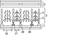
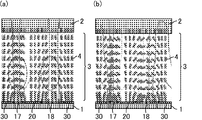
- the inclination size (inclination angle) of the liquid crystal molecules 4 can be made different between the narrow spacing region 17 and the wide spacing region 18. More specifically, as shown in FIG. 4A, the tilt angle of the liquid crystal molecules 4b in the narrowly spaced region 17 is large, and the tilt angle of the liquid crystal molecules 4a in the widely spaced region 18 is small. That is, in the TBA mode liquid crystal display device of this embodiment, the threshold value of the VT characteristic can be changed by changing the electrode interval S, and more specifically, the threshold value can be increased by increasing the electrode interval S. The threshold can be lowered by increasing the value and conversely decreasing the value.
- the threshold value of the VT characteristic is high in the wide space region 18, the liquid crystal molecules 4a in the wide space region 18 are not inclined so much as shown in FIG. As shown, it is circular. That is, in the wide space area 18, almost black is displayed.
- the threshold value of the VT characteristic is low in the narrowly spaced region 17, the liquid crystal molecules 4b in the narrowly spaced region 17 are relatively largely inclined and become elliptical as shown in FIG. That is, gray is displayed in the narrow space region 17.
- the gray of the narrow space 17 is interlaced with the gray of the narrow space 17, and the display (brightness) of the narrow space 17 and the wide space 18 is averaged. As a result, it is visually recognized as gray as a whole.
- the liquid crystal molecules 4a in the wide interval region 18 are elliptical as shown in FIG. 4C, and the liquid crystal molecules 4b in the narrow interval region 17 are rod-like. It becomes a nearly oval shape. That is, gray is displayed in both areas 17 and 18.
- a plurality of regions having different tilt angles of liquid crystal molecules can be formed by making a picture element multi-domain and giving each domain VT characteristics having different threshold values.
- the difference between the threshold value of the VT characteristic of the wide interval region 18 and the threshold value of the VT characteristic of the narrow interval region 17 is preferably about 1.0 V or more. Thereby, whitening can be suppressed more effectively.
- the VT characteristic (VT total ) of the entire picture element obtained by combining the VT characteristics (VT 18 ) of the wide interval region 18 can be changed gently, particularly at a low gradation close to black.
- the gradient of the VT characteristic (VT total ) can be made gentle especially at low gradations.
- the curve of the VT characteristic (VT front ) when observed from the front direction and the curve of the VT characteristic (VT oblique ) when observed from the oblique direction You can also gently bring them closer together. That is, the polar angle dependency of the VT characteristic (change in the VT characteristic when the polar angle is changed) can be reduced. This also shows that according to this embodiment, whitening can be suppressed.
- An equivalent circuit in the picture element portion of the liquid crystal display device of the present embodiment is as shown in FIG. 7, and the liquid crystal capacitance C17 in the narrow spacing region 17 and the liquid crystal capacitance C18 in the wide spacing region 18 are connected in parallel.
- an image signal is input to both capacitors C17 and C18 via the TFT 14 connected to the gate bus line 11 and the source bus line 13.
- the image signals are directly input to the capacitors C17 and C18 from the source bus line 13 via the TFT. Therefore, it is possible to effectively suppress display burn-in as in the technique described in Patent Document 1.
- the picture element configuration of the present embodiment is very simple, and furthermore, whitening can be suppressed only by adjusting the electrode spacing S. Therefore, compared with the technique described in Patent Document 2, the process can be simplified and the cost can be reduced.
- the liquid crystal display device of this comparative embodiment is not provided with the narrowly spaced region 17 and only the widely spaced region 18 is formed in each picture element. It has the same configuration as the device.
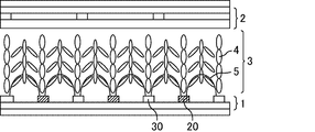
- the liquid crystal layer 3 when no voltage is applied, the liquid crystal layer 3 exhibits homeotropic alignment as shown in FIG.
- FIG. 10 is a diagram schematically showing the behavior of the liquid crystal when a voltage is applied in this comparative embodiment.
- the inclination angle of the liquid crystal molecules 4 is similarly small in all the regions of the picture element.
- a circular shape is obtained as shown in FIG. 11B. That is, when viewed from the front direction during low gradation display, it is visually recognized as almost black.
- the liquid crystal molecules 4 are observed from an oblique direction, the liquid crystal molecules 4 become elliptical as shown in FIG. Therefore, light is leaked when observed from an oblique direction during low gradation display. That is, whitening is confirmed.
- the tilt angle of the liquid crystal molecules when a voltage is applied is also uniform within the picture element. For this reason, as shown in FIG. 12, the VT characteristic of this comparative embodiment changes sharply at a low gradation close to black.
- the curve of the VT characteristic (VT front ) when observed from the front direction and the curve of the VT characteristic (VT oblique ) when observed from the oblique direction are both. It is steep and the two are greatly different. That is, the polar angle dependence of the VT characteristic is large. This also indicates that whitening occurs in this comparative embodiment.
- FIG. 14 is a schematic plan view showing the configuration of the picture elements used in the simulation (three-dimensional simulation).
- the pixel electrode 20 and the common electrode 30 are arranged along the vertical direction.
- the absorption axis directions 6 a and 7 a of the linear polarizing plate are arranged in a direction formed by 45 ° with respect to the extending direction of the pixel electrode 20 and the common electrode 30.
- FIG. 15 shows VT characteristics of the entire picture element of the liquid crystal display device of Embodiment 1 when the ratio to w is 1: 1.
- the VT characteristics of the entire picture element are obtained by calculating the VT characteristics of the narrow spacing region 17 and the VT characteristics of the wide spacing region 18 using the model shown in FIG. Sought by.
- the vertical axis of the VT characteristic graph indicates the transmittance (relative transmittance) when the transmittance at white display (at 256 gradation display) is 1.
- the VT characteristic when observed from the front direction and the VT characteristic when observed from the oblique direction were confirmed to change slowly.
- the oblique direction (azimuth 45 °, polar angle 60 °) is a direction inclined by 45 ° and 60 ° from the front direction.
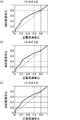
- FIG. 17 shows the whitening characteristics ( ⁇ shift) of the liquid crystal display device of Embodiment 1 calculated based on the results of FIG.
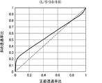
- FIG. 18 shows the whitening characteristics ( ⁇ shift) of the liquid crystal display device of Comparative Example 1 calculated based on the result of FIG.
- the relative transmittance (frontal transmittance ratio) when observed from the front direction is taken on the horizontal axis, and observed from an oblique direction (azimuth 45 °, polar angle 60 °).
- the relative transmittance (oblique transmittance ratio) is plotted on the vertical axis.
- the oblique transmittance ratio when the front transmittance ratio is 0.1 is 0.36.
- the front transmittance ratio is 0.2 (corresponding to 128 gradations out of 256 gradations)
- the oblique transmittance ratio is 0.43. That is, in Comparative Example 1, it was found that the oblique transmittance ratio became larger with respect to the front transmittance ratio, particularly from the low gradation to the halftone, and whitening occurred remarkably.
- the oblique transmittance ratio when the front transmittance ratio is 0.1 is 0.26, and the front transmittance ratio is 0.2.
- the oblique transmittance ratio was 0.36. That is, it was found that the oblique transmittance ratio can be made closer to the front transmittance ratio, particularly from low gradation to halftone, and whitening can be suppressed.
- human vision is particularly sensitive to changes in transmittance from low gradation to halftone display. That is, in the first embodiment, since the difference between the front transmittance ratio and the oblique transmittance ratio is small, particularly from the low gradation to the halftone, it is possible to more effectively suppress the whitening. .
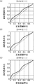
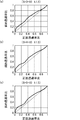
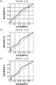
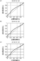
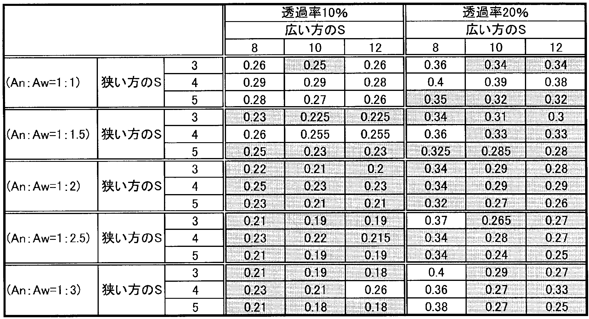
- the ratio A n between the area A w of the area A n and the wide-interval area 18 of the narrow-interval area 17 The A w while varying showing the results of examining the whitening characteristics of the first embodiment by.
- the electrode spacing S of the narrow spacing region 17 was set to 3, 4 or 5 ⁇ m, and the electrode spacing S of the wide spacing region 18 was set to 8, 10 or 12 ⁇ m.
- the electrode width L was fixed at 2.5 ⁇ m for both the narrow spacing region 17 and the wide spacing region 18. Then, A n: an A w, 1: 1,1: 1.5,1 : 2,1: 2.5 or 1: set to 3.
- the size of the A n below the size of the A w, it can be generated trough in the graph of whitening properties (recessed portion) on the low gradation side.
- the difference between the front transmittance ratio and the oblique transmittance ratio can be reduced on the low gradation side, it is possible to effectively suppress whitening.
- a n may be greater than the A w, but in this case, the valley of the graph of whitish characteristic is shifted to the high gradation side. That is, the difference between the front transmittance ratio and the oblique transmittance ratio on the high gradation side is reduced, but the difference between the front transmittance ratio and the oblique transmittance ratio on the low gradation side is not so reduced.
- the effect of suppressing excess brightness becomes smaller.
- human vision is sensitive to changes in transmittance from low gradation to halftone display, so the difference between the front transmittance ratio and the oblique transmittance ratio is reduced on the high gradation side. Even so, the effect of improving the display quality is small.
- the A n is larger than A w, becomes many number of branch portions 22 and 32 provided in the picture element. Since the branches 22 and 32 are regions where light is not transmitted, in this case, the transmittance is reduced.
- FIG. 34 shows the result of examining the white floating characteristics of a commercially available MVA mode television.
- This television employs a driving method using multiple pixels. That is, similarly to the technique described in Patent Document 2, a high-luminance sub-picture element and a low-luminance sub-picture element are driven using two TFTs, and the luminance of the picture elements is averaged and displayed. This is a method that is excellent in suppressing whitening.
- the relative luminance (corresponding to the oblique transmittance ratio) at 96 gradations is 0.25, and 128 gradations (frontal ratio).
- the liquid crystal display device of the first embodiment in the TBA mode as shown in Table 1, the whitening suppression superior to that of the MVA mode television can be achieved without adopting a driving method using multiple pixels. It turned out that an effect can be demonstrated.
- the oblique transmittance ratio superior to that of the MVA mode television is painted in gray.
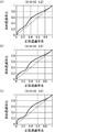
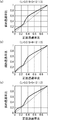
- the electrode width L is fixed to 3.0 ⁇ m for both the narrow spacing region 17 and the wide spacing region 18, the electrode spacing S of the narrow spacing region 17 is set to 3, 4 or 5 ⁇ m, and the electrode spacing S of the wide spacing region 18 is set.
- region 18 was set to 1: 1, 1: 2 or 1: 3.
- FIG. 44 shows the result of examining the white floating characteristics in the comparative example 1 by changing the electrode width L from 2.5 ⁇ m to 3.0 ⁇ m.
- the electrode width L 3.0 ⁇ m
- the oblique transmittance ratio when the front transmittance ratio is 0.1 is 0.28
- the front transmittance ratio is 0.2.
- the oblique transmittance ratio at that time was 0.36.
- the ratio between the area A w is 1 of the area of the narrow-interval area 17 A n and the wide-interval areas 18: the most whitening is when 2 It turned out that it can suppress.
- FIG. 45 shows the liquid crystal display device according to the first embodiment in which the ratio of the area of the narrow spacing region 17 to the area of the wide spacing region 18 is set to 1: 2.
- a n : A w is adjusted by changing the lengths of the branch portions 22 of the pixel electrodes 20 and the branch portions 32 of the common electrode 30 in the narrow interval region 17 and the wide interval region 18, respectively. be able to.
- a n A w can be easily adjusted by changing the layout of the electrodes. Below, the modification of the pixel pattern in the liquid crystal display device of Embodiment 1 is shown.
- the branch part 22 and the branch part 32 may be bent. Thereby, the electrode interval S is changed stepwise along the extending direction of the branch portion 22 and the branch portion 32.
- a n A w is designed to be 1: 1
- a n A w is designed to be 1: 2.
- 11 indicates a gate bus line
- 12 indicates a Cs bus line
- 13 indicates a source bus line
- 14 indicates a TFT
- 15 indicates a drain wiring
- Reference numeral 19 denotes a contact hole for connecting the drain wiring 15 and the pixel electrode 20.
- L / S of the narrow spacing region 17 is 2.5 ⁇ m / 3.0 ⁇ m
- L / S of the wide spacing region 18 is 2.5 ⁇ m / 8.0 ⁇ m
- d ⁇ n 350 nm
- ⁇ 20.
- a vertical alignment film made of polyimide was formed.
- a negative C plate (retardation in the in-plane direction: 0 nm, normal line) composed of a TAC and a retardation plate between the array substrate 1 and the linear polarizing plate 4 and between the counter substrate 2 and the linear polarizing plate 5, respectively.
- Direction retardation Rth 270 nm).
- An AC voltage (amplitude 0 to 6.5 V, frequency 30 Hz) was applied to the pixel electrode.
- the AC voltage Vc (amplitude center) applied to the pixel electrode was set to the same potential as that of the common electrode.
- a DC voltage having a relative potential of 0 V with respect to Vc of the AC voltage applied to the pixel electrode was applied to the common electrode.
- the oblique transmittance ratio when the front transmittance ratio is 0.1 is 0.30
- the oblique transmittance ratio when the front transmittance ratio is 0.2 is It was 0.37.
- a n: A w 1 : even one actual prototype, whitening is suppressed, was able to exert a whitening characteristics equivalent to TV commercial MVA mode.
- the branch portion 22 and the branch portion 32 may be arranged in an oblique direction when the liquid crystal display panel is viewed from the front.
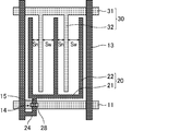
- the trunk portion 21 of the pixel electrode 20 is formed in a T-shape in plan view in the vertical direction and 180 ° direction so as to bisect a rectangular pixel region in plan view. Further, the branch portion 22 of the pixel electrode 20 extends from the trunk portion 21 toward the 135 ° or 225 ° direction. Further, the branch part 32 of the common electrode 30 extends from the trunk part 31 in the 45 ° or 315 ° direction.
- the absorption axis 6a of the linearly polarizing plate 6 is disposed along the vertical direction
- the absorption axis 7a of the linearly polarizing plate 7 is disposed along the left and right direction.
- an excellent contrast ratio can be exhibited in the horizontal and vertical directions. This is particularly preferable when the present embodiment is used for a large-sized liquid crystal display device (in particular, a television).
- the pixel electrode 20 and the common electrode 30 each have two types of branch portions 22 and branch portions 32 whose extending directions are orthogonal to each other. Therefore, two types of bend-shaped electric fields whose electric field directions are orthogonal to each other are formed in one picture element. That is, since two domains are formed in each of the various branches 22 and 32, a total of four domains are formed in one picture element. This makes it possible to compensate for viewing angles without deviation in all directions in the vertical and horizontal directions.
- FIG. 48 the design is such that A n : A w is 1: 2.
- 11 indicates a gate bus line
- 12 indicates a Cs bus line
- 13 indicates a source bus line
- 14 indicates a TFT
- 15 indicates a drain wiring
- 16 indicates , Shows the gate of the TFT 14 and is connected to the gate bus line 11.
- L / S of the narrow spacing region 17 is 2.5 ⁇ m / 3.0 ⁇ m
- L / S of the wide spacing region 18 is 2.5 ⁇ m / 10.0 ⁇ m
- d ⁇ n 350 nm
- ⁇ 20.
- a vertical alignment film made of polyimide was formed.
- a negative C plate (retardation in the in-plane direction: 0 nm, normal line) composed of a TAC and a retardation plate between the array substrate 1 and the linear polarizing plate 4 and between the counter substrate 2 and the linear polarizing plate 5, respectively.
- Direction retardation Rth 270 nm).
- An AC voltage (amplitude 0 to 6.5 V, frequency 30 Hz) was applied to the pixel electrode.
- the AC voltage Vc (amplitude center) applied to the pixel electrode was set to the same potential as that of the common electrode.
- a DC voltage having a relative potential of 0 V with respect to Vc of the AC voltage applied to the pixel electrode was applied to the common electrode.
- the oblique transmittance ratio when the front transmittance ratio is 0.1 is 0.28
- the oblique transmittance ratio when the front transmittance ratio is 0.2 is It was 0.37.
- a n: A w 1 : even in 2 of the actual prototype, whitening is suppressed, was able to exert a whitening characteristics equivalent to TV commercial MVA mode.
- each of the branch part 22 and the branch part 32 may be bent as shown in FIG.
- the design is such that A n : A w is 1: 2.
- the form shown in FIGS. 51 and 52 is preferable.
- the source bus line 13 is bent in a zigzag shape in a V shape, and the portion of the common electrode 30 on the source bus line 13 is also bent in a zigzag shape in a V shape.
- the source bus line 13 has a planar shape in which a portion extending in the 225 ° direction and a portion extending in the 315 ° direction are connected.
- the gate bus line 11 and the Cs bus line 12 are linearly formed in the left-right direction.
- the portion of the trunk 31 that overlaps the source bus line 13 in a plan view is bent zigzag in the 225 ° direction and the 315 ° direction, similarly to the source bus line 13.
- branch portion 32 of the common electrode 30 is connected to a portion overlapping the gate bus line 11 of the trunk portion 31 in a plan view. Further, the branch portion 32 is extended from the upper and lower sides of the picture element toward the center of the picture element, more specifically, from the portion of the trunk portion 31 located above and below the picture element in the direction of 135 ° or 225 °. Yes.
- the trunk 21 is provided in an island shape in the center of the picture element. Further, the branch part 22 of the pixel electrode 20 extends from the center of the picture element to the top and bottom of the picture element, more specifically, from the trunk part 21 toward the 45 ° or 315 ° direction.
- the direction of the electric field generated by the portion overlapping the source bus line 13 of the trunk portion 31 and the branch portion 22 is approximately 45 ° with respect to the absorption axis direction of the pair of linearly polarizing plates.
- the liquid crystal molecules are aligned obliquely with respect to the absorption axis direction of the pair of linearly polarizing plates also in the region sandwiched between the portion of the trunk portion 31 that overlaps the source bus line 13 and the branch portion 22. It becomes. Therefore, light can be transmitted also in this region, and the transmittance can be improved.
- the gate bus line 11 and the Cs bus line 12 may be bent instead of the source bus line 13.
- the gate bus line 11 and the Cs bus line 12 may be bent in a zigzag shape in a V shape, and the portion of the common electrode 30 on the gate bus line 11 may be similarly bent in a zigzag shape in a V shape.
- each of the gate bus line 11 and the Cs bus line 12 has a planar shape in which a portion extending in the 45 ° direction and a portion extending in the 315 ° direction are connected.
- the source bus line 13 is linearly formed in the vertical direction.
- the portion of the trunk portion 31 that overlaps the gate bus line 11 in a plan view is bent zigzag in the 45 ° direction and the 315 ° direction in the same manner as the gate bus line 11.
- the branch portion 32 is connected to a portion of the trunk portion 31 that overlaps the source bus line 13 in plan view. Further, the branch part 32 is extended from the left and right sides of the picture element toward the center of the picture element, more specifically, from the part located on the left and right of the picture element of the trunk part 31 toward the 45 ° or 135 ° direction. Yes.
- the trunk 21 is provided in an island shape in the center of the picture element. Further, the branch portion 22 extends from the center of the picture element to the left and right of the picture element, more specifically, from the trunk portion 21 toward the 225 ° or 315 ° direction.
- the direction of the electric field generated by the portion overlapping the gate bus line 11 of the trunk portion 31 and the branch portion 22 is approximately 45 ° with respect to the absorption axis direction of the pair of linearly polarizing plates.
- the liquid crystal molecules are aligned obliquely with respect to the absorption axis direction of the pair of linearly polarizing plates also in the region sandwiched between the branch portion 22 and the portion that overlaps the gate bus line 11 of the trunk portion 31. It becomes. Therefore, light can be transmitted also in this region.
- a narrow space region 17 and a wide space region 18 are provided in the picture element.
- the electrode spacing S changes stepwise along the extending direction of the branch part 22 and the branch part 32.
- the branch portion 22 or the branch portion from the tip region of the branch portion 22 or the branch portion 32 is maintained while keeping the sum of the electrode interval S in the narrow interval region 17 and the electrode interval S in the wide interval region 18 constant.
- the size of both spaces, that is, both regions 17 and 18 are alternately switched.
- interval differs mutually is not specifically limited to two, Three or more may be sufficient.
- the electrode spacing in each color picture element may be the same or different.
- the electrode spacing in each color picture element can be optimized in accordance with the characteristics of light of a specific color (specific wavelength) that passes through each color picture element.
- FIGS. 53 to 55 are schematic plan views of the liquid crystal display device of Comparative Example 2.
- Embodiment 2 The liquid crystal display device of this embodiment is different from that of Embodiment 1 in the following points. That is, the liquid crystal display device of this embodiment has a counter electrode on the counter substrate 2 side. Specifically, as shown in FIG. 57, the counter electrode 61, the dielectric layer (insulating layer) 62, and the vertical alignment film 51 are stacked in this order on the main surface of the insulating substrate 40 on the liquid crystal layer side. . Note that the color layer 42 and / or the BM layer 41 may be provided between the counter electrode 61 and the insulating substrate 40.
- the counter electrode 61 is formed from a transparent conductive film such as ITO or IZO. Each of the counter electrode 61 and the dielectric layer 62 is formed without a break so as to cover at least the entire display region. A predetermined potential common to each pixel (picture element) is applied to the counter electrode 61.
- the dielectric layer 62 is formed from a transparent insulating material. Specifically, it is formed from an inorganic insulating film such as silicon nitride, an organic insulating film such as acrylic resin, or the like.
- a pair of comb-like electrodes including the pixel electrode 20 and the common electrode 30 are provided on the insulating substrate 10 as in the first embodiment, and a vertical alignment film 52 is further provided. Further, linearly polarizing plates 6 and 7 are disposed on the outer main surfaces of the two insulating substrates 10 and 40.
- the common electrode group 30 and the counter electrode 61 may be grounded, or voltages having the same magnitude and polarity may be applied to the common electrode 30 and the counter electrode 61, or voltages having different magnitudes and polarities from each other. May be applied.
- the whitening phenomenon can be improved as in the first embodiment. Further, the response speed can be improved by forming the counter electrode 61.
- FIG. 58 shows another specific example of the pixel configuration in the first and second embodiments.
- the pixels shown in FIG. 58 may be composed of picture elements (sub-pixels) of a plurality of colors. In this case, the following structure shows the picture elements.
- a source bus line 13 On the main surface of the insulating substrate 10 on the liquid crystal layer 3 side, there are a source bus line 13, a gate bus line 11, a switching element (active element), and a thin film transistor (TFT) provided for each pixel. 14, a pixel electrode 20 provided separately for each pixel, and a common electrode 30 provided in common to a plurality of pixels (for example, all pixels).
- the gate bus line 11 and the common electrode 30 are provided on the insulating substrate 10, a gate insulating film (not shown) is provided on the gate bus line 11 and the common electrode 30, and the source bus line 13 and the pixel electrode 20 are gates.
- a vertical alignment film 52 is provided on the insulating film and on the source bus line 13 and the pixel electrode 20.
- the common electrode 30 and the pixel electrode 20 may be patterned using the same film in the same process by the photolithography method and may be disposed on the same layer (the same insulating film).
- the source bus lines 13 are provided in a straight line parallel to each other, and extend vertically between adjacent pixels.
- the gate bus lines 11 are provided in a straight line parallel to each other, and extend between adjacent pixels in the left-right direction.
- the source bus line 13 and the gate bus line 11 are orthogonal to each other, and a region defined by the source bus line 13 and the gate bus line 11 is approximately one pixel region.
- the gate bus line 11 also functions as the gate of the TFT 14 in the display area.
- the TFT 14 includes a semiconductor layer 28 provided in the vicinity of the intersection of the source bus line 13 and the gate bus line 11 and formed in an island shape on the gate bus line 11.
- the TFT 14 includes a source electrode 24 that functions as a source and a drain wiring 15 that functions as a drain.
- the source electrode 24 connects the TFT 14 and the source bus line 13, and the drain wiring 15 connects the TFT 14 and the pixel electrode 20.
- the source electrode 24 and the source bus line 13 are connected by patterning from the same film.
- the drain wiring 15 and the pixel electrode 20 are connected by patterning from the same film.
- An image signal is supplied from the source bus line 13 to the pixel electrode 20 at a predetermined timing while the TFT 14 is on. On the other hand, a predetermined potential common to each pixel is applied to the common electrode 30.
- the planar shape of the pixel electrode 20 is a comb-teeth shape, and the pixel electrode 20 has a linear trunk (pixel trunk) 21 and a plurality of linear combs (branches 22).
- the trunk portion 21 is provided along the short side (lower side) of the pixel.
- the branch portions 22 are connected to each other by being connected to the trunk portion 21.
- the branch part 22 is extended
- the planar shape of the common electrode 30 is a comb-teeth shape, and includes a linear trunk portion (common trunk portion) 31 and a plurality of linear comb teeth (branch portions 32).
- the branch part 32 and the trunk part 31 are connected by being patterned from the same film.
- the trunk portion 31 is provided in a straight line parallel to the gate bus line 11 and extends between adjacent pixels in the left-right direction.
- the branch portion 32 extends from the trunk portion 31 toward the lower side of the opposing pixel, that is, in a direction of approximately 270 °.
- the pixel electrode 20 and the common electrode 30 are arranged to face each other so that the comb teeth (branches 22 and 32) are engaged with each other. Further, the branch portions 22 and the branch portions 32 are arranged in parallel with each other, and are alternately arranged with an interval.
- two domains in which the tilt directions of liquid crystal molecules are opposite are formed in one pixel.
- the number of domains is not particularly limited and can be set as appropriate. From the viewpoint of obtaining good viewing angle characteristics, four domains may be formed in one pixel.
- the example shown in FIG. 58 has two or more regions having different electrode intervals in one pixel. More specifically, a region with a relatively narrow electrode interval (region of Sn) and a region with a relatively wide electrode interval (region of Sw) are formed in each pixel. As a result, as in the first embodiment, the whitening phenomenon can be improved.
- Liquid crystal display panel 1 Active matrix substrate (TFT array substrate) 2: counter substrate 3: liquid crystal layer 4, 4a, 4b: liquid crystal molecule 5: transverse electric field 6, 7: linearly polarizing plate 6a, 7a: absorption axis 10: insulating substrate 11: gate bus line 12: Cs bus line 13: source Bus line 14: TFT 15: drain wiring 16: gate 17: narrow spacing region 18: wide spacing region 19: contact hole 20: pixel electrode 21: trunk (pixel trunk) 22: Branch (pixel branch) 24: source electrode 28: semiconductor layer 30: common electrode 31: trunk (common trunk) 32: Branch (pixel branch) 40: Insulating substrate 41: BM layer 42: Color layer 43: Overcoat layer 51, 52: Vertical alignment film 61: Counter electrode 62: Dielectric layer
Landscapes
- Physics & Mathematics (AREA)
- Nonlinear Science (AREA)
- Geometry (AREA)
- Mathematical Physics (AREA)
- Chemical & Material Sciences (AREA)
- Crystallography & Structural Chemistry (AREA)
- General Physics & Mathematics (AREA)
- Optics & Photonics (AREA)
- Liquid Crystal (AREA)
Abstract
Description
MVAモード、PVAモード、TBAモード等の表示モードは、通常、クロスニコル設定下で電圧無印加時にネマチック液晶を垂直配向するノーマリーブラックモードである。また、これらのモードは、電圧印加時の視野角を広くするために、電圧印加により液晶分子が正面方向を中心に対称的に傾斜する、いわゆるマルチドメイン(セル内自己補償)構造を有する。ただし、これらのモードにおいては、正面方向と斜め方向とでの電圧-透過率特性(VT特性)の形状が異なるという課題がある。この課題は、黒表示に近い階調(低階調)において特に顕著であり、低階調ではVT特性が極角の変化に大きく依存する。具体的には、観察方向を正面方向から倒した時に、低階調側の暗い表示が白く浮いてくる(白っぽくなる)現象が発生する。なお、この現象は白浮きとも呼ばれる。また、この白浮き現象は、白黒表示では視認されない。なお、ここでの白黒表示とは、複数色の絵素(通常、R(赤)、G(緑)、B(青)の絵素)の明るさを調整して白黒表示を行うことを意味する。
本発明の液晶表示装置における好ましい形態について以下に詳しく説明する。
本実施形態の液晶表示装置は、液晶層に対して基板面方向(基板面に対して平行な方向)の電界(横電界)を作用させ、液晶の配向を制御することにより画像表示を行う横電界方式のうち、TBA方式(TBAモード)と呼ばれる方式を採用した透過型の液晶表示装置である。
・狭間隔領域17のL/S=2.5μm/3.0μm(すなわちL=2.5μm、S=3.0μm)
・広間隔領域18のL/S=2.5μm/8.0μm(すなわちL=2.5μm、S=8.0μm)
・dΔn:350nm
・Δε:20
・γ1(液晶の回転粘度):200
・アレイ基板1及び直線偏光板6の間と、対向基板2及び直線偏光板7の間とにそれぞれ、光学補償板としてネガティブCプレート単層(面内方向のリタデーションRe:0nm、法線方向のリタデーションRth:270nm)を配置
・画素電極:AC印加(振幅0~6.5V、周波数30Hz)
ただし、Vc(振幅センター)は、共通電極と同電位に設定
・共通電極:画素電極のVcに対する相対電位が0VのDC印加
本比較形態の液晶表示装置は、図8に示すように、狭間隔領域17が設けられず、各絵素内に広間隔領域18のみが形成されていること以外は、実施形態1の液晶表示装置と同様の構成を有する。
・dΔn:350nm
・Δε:20
・γ1:200
・アレイ基板1及び直線偏光板6の間と、対向基板2及び直線偏光板7の間とにそれぞれ、光学補償板としてネガティブCプレート単層(面内方向のリタデーションRe:0nm、法線方向のリタデーションRth:270nm)を配置
・画素電極:AC印加(振幅0~6.5V、周波数30Hz)
ただし、Vc(振幅センター)は、共通電極と同電位に設定
・共通電極:画素電極のVcに対する相対電位が0VのDC印加
なお、以下に示すシミュレーションについても、特に断りがない限り、この条件を用いた。

枝部22及び枝部32は、図48に示すように、液晶表示パネルを正面視したときに、斜め方向に配置されてもよい。
図48に示した絵素パターンにおいて、枝部22及び枝部32はそれぞれ、図50に示すように折れ曲がっていてもよい。なお、図50では、An:Awが1:2になるように設計されている。
図53~55に比較形態2の液晶表示装置の平面模式図を示す。本比較形態の液晶表示装置は、図53~55に示すように、実施形態1と同様に櫛歯状の画素電極20及び共通電極30を有するが、電極間隔が絵素内で統一されているため、白浮きが顕著に視認されてしまう。
本実施形態の液晶表示装置は、以下の点で実施形態1と異なる。
すなわち、本実施形態の液晶表示装置は、対向基板2側に対向電極を有する。具体的には、図57に示すように、絶縁基板40の液晶層側の主面上には、対向電極61、誘電体層(絶縁層)62及び垂直配向膜51がこの順に積層されている。なお、対向電極61と絶縁基板40の間には、色層42及び/又はBM層41等が設けられてもよい。
1:アクティブマトリクス基板(TFTアレイ基板)
2:対向基板
3:液晶層
4、4a、4b:液晶分子
5:横電界
6、7:直線偏光板
6a、7a:吸収軸
10:絶縁基板
11:ゲートバスライン
12:Csバスライン
13:ソースバスライン
14:TFT
15:ドレイン配線
16:ゲート
17:狭間隔領域
18:広間隔領域
19:コンタクトホール
20:画素電極
21:幹部(画素幹部)
22:枝部(画素枝部)
24:ソース電極
28:半導体層
30:共通電極
31:幹部(共通幹部)
32:枝部(画素枝部)
40:絶縁基板
41:BM層
42:色層
43:オーバーコート層
51、52:垂直配向膜
61:対向電極
62:誘電体層
Claims (5)
- 互いに対向配置された一対の基板と、前記一対の基板間に挟持された液晶層とを備える液晶表示装置であって、
前記一対の基板の一方は、櫛歯状の一対の電極を有し、
前記一対の電極は、画素内において互いに平面的に対向配置され、
前記液晶層は、p型ネマチック液晶を含むとともに、前記一対の電極間に生じる電界によって駆動され、
前記p型ネマチック液晶は、電圧無印加時に、前記一対の基板面に対して垂直に配向し、
前記液晶表示装置は、画素内に前記一対の電極の間隔が互いに異なる2つ以上の領域を有することを特徴とする液晶表示装置。 - 前記液晶表示装置は、前記間隔が互いに異なる2つの領域を有し、
前記2つの領域の内の前記間隔が狭い方の面積をAnとし、前記2つの領域の内の前記間隔が広い方の面積Awをとすると、前記液晶表示装置は、An≦Awを満たすことを特徴とする請求項1記載の液晶表示装置。 - 前記液晶表示装置は、An:Aw=1:1~1:3を満たすことを特徴とする請求項2記載の液晶表示装置。
- 前記液晶表示装置は、An:Aw=1:1.5~1:3を満たすことを特徴とする請求項3記載の液晶表示装置。
- 前記液晶表示装置は、実質的にAn:Aw=1:2を満たすことを特徴とする請求項4記載の液晶表示装置。
Priority Applications (4)
| Application Number | Priority Date | Filing Date | Title |
|---|---|---|---|
| US13/322,206 US20120069282A1 (en) | 2009-05-28 | 2010-04-20 | Liquid crystal display device |
| JP2011515954A JPWO2010137427A1 (ja) | 2009-05-28 | 2010-04-20 | 液晶表示装置 |
| EP10780384A EP2437112A4 (en) | 2009-05-28 | 2010-04-20 | LIQUID CRYSTAL DISPLAY DEVICE |
| CN201080022935XA CN102449545A (zh) | 2009-05-28 | 2010-04-20 | 液晶显示装置 |
Applications Claiming Priority (4)
| Application Number | Priority Date | Filing Date | Title |
|---|---|---|---|
| JP2009-129521 | 2009-05-28 | ||
| JP2009129521 | 2009-05-28 | ||
| JP2010-006693 | 2010-01-15 | ||
| JP2010006693 | 2010-01-15 |
Publications (1)
| Publication Number | Publication Date |
|---|---|
| WO2010137427A1 true WO2010137427A1 (ja) | 2010-12-02 |
Family
ID=43222544
Family Applications (1)
| Application Number | Title | Priority Date | Filing Date |
|---|---|---|---|
| PCT/JP2010/057006 Ceased WO2010137427A1 (ja) | 2009-05-28 | 2010-04-20 | 液晶表示装置 |
Country Status (5)
| Country | Link |
|---|---|
| US (1) | US20120069282A1 (ja) |
| EP (1) | EP2437112A4 (ja) |
| JP (1) | JPWO2010137427A1 (ja) |
| CN (1) | CN102449545A (ja) |
| WO (1) | WO2010137427A1 (ja) |
Cited By (6)
| Publication number | Priority date | Publication date | Assignee | Title |
|---|---|---|---|---|
| CN102854675A (zh) * | 2012-01-10 | 2013-01-02 | 友达光电股份有限公司 | 液晶显示装置 |
| JP2013142900A (ja) * | 2012-01-10 | 2013-07-22 | Au Optronics Corp | 液晶表示装置 |
| WO2014050672A1 (ja) * | 2012-09-26 | 2014-04-03 | シャープ株式会社 | 液晶表示装置 |
| WO2014171202A1 (ja) * | 2013-04-19 | 2014-10-23 | シャープ株式会社 | 液晶表示装置 |
| KR20160115816A (ko) * | 2015-03-26 | 2016-10-06 | 가부시키가이샤 한도오따이 에네루기 켄큐쇼 | 표시 장치, 해당 표시 장치를 갖는 표시 모듈 및 해당 표시 장치 또는 해당 표시 모듈을 갖는 전자 기기 |
| JP2018106074A (ja) * | 2016-12-27 | 2018-07-05 | 株式会社 オルタステクノロジー | 液晶表示装置 |
Families Citing this family (7)
| Publication number | Priority date | Publication date | Assignee | Title |
|---|---|---|---|---|
| CN104024933B (zh) * | 2011-10-31 | 2016-05-25 | 夏普株式会社 | 薄膜晶体管阵列基板和液晶显示装置 |
| CN104267549B (zh) * | 2014-10-14 | 2017-04-12 | 深圳市华星光电技术有限公司 | 液晶显示面板及其阵列基板 |
| CN104808401B (zh) * | 2015-04-15 | 2018-01-26 | 深圳市华星光电技术有限公司 | 一种液晶显示面板 |
| GB2566673B (en) * | 2017-07-21 | 2022-10-26 | Flexenable Ltd | Thin-Film Transistor (TFT) Architecture for Liquid Crystal Displays |
| CN107315288B (zh) * | 2017-08-17 | 2021-01-26 | 京东方科技集团股份有限公司 | 一种阵列基板、液晶面板及其制作工艺 |
| CN108388052B (zh) * | 2018-03-01 | 2022-07-26 | 上海天马微电子有限公司 | 一种显示面板及显示装置 |
| CN111522164A (zh) * | 2019-02-01 | 2020-08-11 | 群创光电股份有限公司 | 电子装置 |
Citations (9)
| Publication number | Priority date | Publication date | Assignee | Title |
|---|---|---|---|---|
| JPH0792504A (ja) | 1993-09-20 | 1995-04-07 | Toshiba Corp | 液晶表示装置 |
| JPH10186351A (ja) * | 1996-12-24 | 1998-07-14 | Hitachi Ltd | 液晶表示装置 |
| JP2005292397A (ja) | 2004-03-31 | 2005-10-20 | Fujitsu Display Technologies Corp | 液晶表示装置 |
| JP2005316211A (ja) | 2004-04-30 | 2005-11-10 | Fujitsu Display Technologies Corp | 視角特性を改善した液晶表示装置 |
| WO2008001507A1 (en) * | 2006-06-26 | 2008-01-03 | Sharp Kabushiki Kaisha | Display |
| JP2008112021A (ja) * | 2006-10-31 | 2008-05-15 | Seiko Epson Corp | 液晶装置及び電子機器 |
| JP2009129521A (ja) | 2007-11-27 | 2009-06-11 | Panasonic Corp | 楽曲再生装置 |
| WO2009139198A1 (ja) * | 2008-05-12 | 2009-11-19 | シャープ株式会社 | 液晶表示装置 |
| JP2010006693A (ja) | 2008-06-20 | 2010-01-14 | Soc Europeenne De Systemes Optiques | 非球面光学素子の形成方法 |
Family Cites Families (13)
| Publication number | Priority date | Publication date | Assignee | Title |
|---|---|---|---|---|
| KR100258435B1 (ko) * | 1996-10-22 | 2000-06-01 | 윤종용 | 평면 구동 방식의 액정 표시 장치용 기판 |
| JP4201942B2 (ja) * | 1999-12-02 | 2008-12-24 | シャープ株式会社 | 液晶表示装置 |
| JP2000275682A (ja) * | 1999-03-26 | 2000-10-06 | Seiko Epson Corp | 液晶装置およびそれを用いた電子機器 |
| KR100607741B1 (ko) * | 2000-05-24 | 2006-08-01 | 엘지.필립스 엘시디 주식회사 | 칼라 액정표시장치 |
| SE0303041D0 (sv) * | 2003-06-23 | 2003-11-18 | Ecsibeo Ab | A liquid crystal device and a method for manufacturing thereof |
| KR101112584B1 (ko) * | 2004-12-27 | 2012-02-15 | 엘지디스플레이 주식회사 | 횡전계형 액정표시장치 |
| JP4138759B2 (ja) * | 2005-02-03 | 2008-08-27 | セイコーエプソン株式会社 | 液晶表示装置および電子機器 |
| JP4476137B2 (ja) * | 2005-02-28 | 2010-06-09 | セイコーエプソン株式会社 | 液晶装置および電子機器 |
| JP2007004126A (ja) * | 2005-05-25 | 2007-01-11 | Sanyo Epson Imaging Devices Corp | 液晶装置及び電子機器 |
| JP4762682B2 (ja) * | 2005-11-07 | 2011-08-31 | 株式会社 日立ディスプレイズ | 半透過型液晶表示装置 |
| KR101382481B1 (ko) * | 2007-09-03 | 2014-04-09 | 삼성디스플레이 주식회사 | 표시 장치 |
| JP5429584B2 (ja) * | 2007-09-26 | 2014-02-26 | Nltテクノロジー株式会社 | 表示装置及びそれらを用いた携帯機器、端末装置 |
| US8169559B2 (en) * | 2009-01-16 | 2012-05-01 | Samsung Electronics Co., Ltd. | Array substrate and method of manufacturing the same |
-
2010
- 2010-04-20 JP JP2011515954A patent/JPWO2010137427A1/ja active Pending
- 2010-04-20 WO PCT/JP2010/057006 patent/WO2010137427A1/ja not_active Ceased
- 2010-04-20 EP EP10780384A patent/EP2437112A4/en not_active Withdrawn
- 2010-04-20 US US13/322,206 patent/US20120069282A1/en not_active Abandoned
- 2010-04-20 CN CN201080022935XA patent/CN102449545A/zh active Pending
Patent Citations (9)
| Publication number | Priority date | Publication date | Assignee | Title |
|---|---|---|---|---|
| JPH0792504A (ja) | 1993-09-20 | 1995-04-07 | Toshiba Corp | 液晶表示装置 |
| JPH10186351A (ja) * | 1996-12-24 | 1998-07-14 | Hitachi Ltd | 液晶表示装置 |
| JP2005292397A (ja) | 2004-03-31 | 2005-10-20 | Fujitsu Display Technologies Corp | 液晶表示装置 |
| JP2005316211A (ja) | 2004-04-30 | 2005-11-10 | Fujitsu Display Technologies Corp | 視角特性を改善した液晶表示装置 |
| WO2008001507A1 (en) * | 2006-06-26 | 2008-01-03 | Sharp Kabushiki Kaisha | Display |
| JP2008112021A (ja) * | 2006-10-31 | 2008-05-15 | Seiko Epson Corp | 液晶装置及び電子機器 |
| JP2009129521A (ja) | 2007-11-27 | 2009-06-11 | Panasonic Corp | 楽曲再生装置 |
| WO2009139198A1 (ja) * | 2008-05-12 | 2009-11-19 | シャープ株式会社 | 液晶表示装置 |
| JP2010006693A (ja) | 2008-06-20 | 2010-01-14 | Soc Europeenne De Systemes Optiques | 非球面光学素子の形成方法 |
Non-Patent Citations (1)
| Title |
|---|
| See also references of EP2437112A4 |
Cited By (11)
| Publication number | Priority date | Publication date | Assignee | Title |
|---|---|---|---|---|
| CN102854675A (zh) * | 2012-01-10 | 2013-01-02 | 友达光电股份有限公司 | 液晶显示装置 |
| JP2013142900A (ja) * | 2012-01-10 | 2013-07-22 | Au Optronics Corp | 液晶表示装置 |
| CN102854675B (zh) * | 2012-01-10 | 2015-06-10 | 友达光电股份有限公司 | 液晶显示装置 |
| WO2014050672A1 (ja) * | 2012-09-26 | 2014-04-03 | シャープ株式会社 | 液晶表示装置 |
| WO2014171202A1 (ja) * | 2013-04-19 | 2014-10-23 | シャープ株式会社 | 液晶表示装置 |
| JPWO2014171202A1 (ja) * | 2013-04-19 | 2017-02-16 | シャープ株式会社 | 液晶表示装置 |
| KR20160115816A (ko) * | 2015-03-26 | 2016-10-06 | 가부시키가이샤 한도오따이 에네루기 켄큐쇼 | 표시 장치, 해당 표시 장치를 갖는 표시 모듈 및 해당 표시 장치 또는 해당 표시 모듈을 갖는 전자 기기 |
| JP2016184163A (ja) * | 2015-03-26 | 2016-10-20 | 株式会社半導体エネルギー研究所 | 表示装置、該表示装置を有する表示モジュール、及び該表示装置または該表示モジュールを有する電子機器 |
| US10996524B2 (en) | 2015-03-26 | 2021-05-04 | Semiconductor Energy Laboratory Co., Ltd. | Display device, display module including the display device, and electronic device including the display device or the display module |
| KR102436307B1 (ko) | 2015-03-26 | 2022-08-25 | 가부시키가이샤 한도오따이 에네루기 켄큐쇼 | 표시 장치, 해당 표시 장치를 갖는 표시 모듈 및 해당 표시 장치 또는 해당 표시 모듈을 갖는 전자 기기 |
| JP2018106074A (ja) * | 2016-12-27 | 2018-07-05 | 株式会社 オルタステクノロジー | 液晶表示装置 |
Also Published As
| Publication number | Publication date |
|---|---|
| CN102449545A (zh) | 2012-05-09 |
| EP2437112A4 (en) | 2012-12-26 |
| JPWO2010137427A1 (ja) | 2012-11-12 |
| EP2437112A1 (en) | 2012-04-04 |
| US20120069282A1 (en) | 2012-03-22 |
Similar Documents
| Publication | Publication Date | Title |
|---|---|---|
| US8421975B2 (en) | Liquid crystal display device | |
| WO2010137427A1 (ja) | 液晶表示装置 | |
| JP5253585B2 (ja) | 液晶表示装置 | |
| WO2011040080A1 (ja) | 液晶表示装置 | |
| KR101147090B1 (ko) | 액정표시소자 | |
| CN102472933A (zh) | 液晶显示装置 | |
| RU2509326C1 (ru) | Жидкокристаллическое устройство отображения | |
| CN102449546B (zh) | 液晶显示装置 | |
| CN106444172A (zh) | 液晶显示设备 | |
| US20110317118A1 (en) | Liquid crystal display device | |
| JP3519573B2 (ja) | 液晶表示装置 | |
| US8860916B2 (en) | Liquid crystal display device | |
| WO2011086742A1 (ja) | 液晶表示パネル及び液晶表示装置 | |
| WO2011001742A1 (ja) | 液晶表示装置 | |
| US8907938B2 (en) | Liquid crystal display device | |
| JP5507233B2 (ja) | 液晶表示装置 | |
| WO2009101734A1 (ja) | 液晶表示素子およびそれを備えた表示装置 | |
| JP2008076978A (ja) | 液晶表示装置 | |
| KR20040019141A (ko) | 흑백 박막트랜지스터 액정 디스플레이 장치 | |
| KR20070016952A (ko) | 액정 표시 장치 |
Legal Events
| Date | Code | Title | Description |
|---|---|---|---|
| WWE | Wipo information: entry into national phase |
Ref document number: 201080022935.X Country of ref document: CN |
|
| 121 | Ep: the epo has been informed by wipo that ep was designated in this application |
Ref document number: 10780384 Country of ref document: EP Kind code of ref document: A1 |
|
| WWE | Wipo information: entry into national phase |
Ref document number: 2011515954 Country of ref document: JP |
|
| WWE | Wipo information: entry into national phase |
Ref document number: 13322206 Country of ref document: US |
|
| NENP | Non-entry into the national phase |
Ref country code: DE |
|
| WWE | Wipo information: entry into national phase |
Ref document number: 2010780384 Country of ref document: EP |