WO2010143342A1 - Cellule solaire à semi-conducteur au nitrure - Google Patents
Cellule solaire à semi-conducteur au nitrure Download PDFInfo
- Publication number
- WO2010143342A1 WO2010143342A1 PCT/JP2010/001884 JP2010001884W WO2010143342A1 WO 2010143342 A1 WO2010143342 A1 WO 2010143342A1 JP 2010001884 W JP2010001884 W JP 2010001884W WO 2010143342 A1 WO2010143342 A1 WO 2010143342A1
- Authority
- WO
- WIPO (PCT)
- Prior art keywords
- layer
- semiconductor layer
- semiconductor
- solar cell
- nitride semiconductor
- Prior art date
- Legal status (The legal status is an assumption and is not a legal conclusion. Google has not performed a legal analysis and makes no representation as to the accuracy of the status listed.)
- Ceased
Links
Images


Classifications
-
- H—ELECTRICITY
- H10—SEMICONDUCTOR DEVICES; ELECTRIC SOLID-STATE DEVICES NOT OTHERWISE PROVIDED FOR
- H10F—INORGANIC SEMICONDUCTOR DEVICES SENSITIVE TO INFRARED RADIATION, LIGHT, ELECTROMAGNETIC RADIATION OF SHORTER WAVELENGTH OR CORPUSCULAR RADIATION
- H10F77/00—Constructional details of devices covered by this subclass
- H10F77/70—Surface textures, e.g. pyramid structures
-
- H—ELECTRICITY
- H10—SEMICONDUCTOR DEVICES; ELECTRIC SOLID-STATE DEVICES NOT OTHERWISE PROVIDED FOR
- H10F—INORGANIC SEMICONDUCTOR DEVICES SENSITIVE TO INFRARED RADIATION, LIGHT, ELECTROMAGNETIC RADIATION OF SHORTER WAVELENGTH OR CORPUSCULAR RADIATION
- H10F10/00—Individual photovoltaic cells, e.g. solar cells
- H10F10/10—Individual photovoltaic cells, e.g. solar cells having potential barriers
- H10F10/14—Photovoltaic cells having only PN homojunction potential barriers
- H10F10/142—Photovoltaic cells having only PN homojunction potential barriers comprising multiple PN homojunctions, e.g. tandem cells
-
- H—ELECTRICITY
- H10—SEMICONDUCTOR DEVICES; ELECTRIC SOLID-STATE DEVICES NOT OTHERWISE PROVIDED FOR
- H10F—INORGANIC SEMICONDUCTOR DEVICES SENSITIVE TO INFRARED RADIATION, LIGHT, ELECTROMAGNETIC RADIATION OF SHORTER WAVELENGTH OR CORPUSCULAR RADIATION
- H10F10/00—Individual photovoltaic cells, e.g. solar cells
- H10F10/10—Individual photovoltaic cells, e.g. solar cells having potential barriers
- H10F10/14—Photovoltaic cells having only PN homojunction potential barriers
- H10F10/144—Photovoltaic cells having only PN homojunction potential barriers comprising only Group III-V materials, e.g. GaAs,AlGaAs, or InP photovoltaic cells
-
- H—ELECTRICITY
- H10—SEMICONDUCTOR DEVICES; ELECTRIC SOLID-STATE DEVICES NOT OTHERWISE PROVIDED FOR
- H10F—INORGANIC SEMICONDUCTOR DEVICES SENSITIVE TO INFRARED RADIATION, LIGHT, ELECTROMAGNETIC RADIATION OF SHORTER WAVELENGTH OR CORPUSCULAR RADIATION
- H10F77/00—Constructional details of devices covered by this subclass
- H10F77/70—Surface textures, e.g. pyramid structures
- H10F77/703—Surface textures, e.g. pyramid structures of the semiconductor bodies, e.g. textured active layers
-
- Y—GENERAL TAGGING OF NEW TECHNOLOGICAL DEVELOPMENTS; GENERAL TAGGING OF CROSS-SECTIONAL TECHNOLOGIES SPANNING OVER SEVERAL SECTIONS OF THE IPC; TECHNICAL SUBJECTS COVERED BY FORMER USPC CROSS-REFERENCE ART COLLECTIONS [XRACs] AND DIGESTS
- Y02—TECHNOLOGIES OR APPLICATIONS FOR MITIGATION OR ADAPTATION AGAINST CLIMATE CHANGE
- Y02E—REDUCTION OF GREENHOUSE GAS [GHG] EMISSIONS, RELATED TO ENERGY GENERATION, TRANSMISSION OR DISTRIBUTION
- Y02E10/00—Energy generation through renewable energy sources
- Y02E10/50—Photovoltaic [PV] energy
- Y02E10/544—Solar cells from Group III-V materials
Definitions
- the present invention relates to a thin-film nitride semiconductor solar cell that can be used for photovoltaic power generation.
- a device for realizing this is a solar cell, and electric power can be obtained by taking out an electron-hole pair generated when a semiconductor pn junction is irradiated with light as a photocurrent.
- GaN-based semiconductor Group III-V nitride compound semiconductor represented by gallium nitride (GaN) (general formula In x Al y Ga 1-xy N (where 0 ⁇ x ⁇ 1, 0 ⁇ y ⁇ 1, 0 ⁇ x + y ⁇ (Hereinafter referred to as GaN-based semiconductor) is a material that can cover a wide wavelength band from the ultraviolet region to the infrared region by changing its composition. Therefore, if a GaN-based semiconductor can be stacked as a tandem structure, a more efficient solar cell can be expected.
- GaN-based semiconductor general formula In x Al y Ga 1-xy N (where 0 ⁇ x ⁇ 1, 0 ⁇ y ⁇ 1, 0 ⁇ x + y ⁇ (Hereinafter referred to as GaN-based semiconductor) is a material that can cover a wide wavelength band from the ultraviolet region to the infrared region by changing its composition. Therefore, if a GaN-based semiconductor can be
- the GaN-based semiconductor cannot sufficiently increase the carrier concentration value of the p-type layer in particular, it is difficult to realize a p + n + junction that can obtain a necessary tunnel current by the GaN-based semiconductor. That is, a solar cell using a GaN-based semiconductor has a problem that a good tandem structure cannot be realized and high-efficiency operation cannot be performed.
- the present invention has been made in view of the above-described conventional problems, and an object thereof is to realize a good tandem structure in a solar cell made of a GaN-based semiconductor.
- a nitride semiconductor solar cell is provided with an oxide layer containing zinc between a plurality of nitride semiconductor layers including a pn junction.
- a nitride semiconductor solar cell includes a first semiconductor layer made of a III-V nitride semiconductor and including a first pn junction, and a first semiconductor layer made of a III-V nitride semiconductor.
- the semiconductor layer is formed in ohmic contact with each of a second semiconductor layer including a second pn junction having a different forbidden band width, and between the first semiconductor layer and the second semiconductor layer, and zinc is used.
- an oxide layer including the oxide layer is
- each of the group III-V nitride semiconductors is formed in ohmic contact with each of the first semiconductor layer and the second semiconductor layer including the pn junction,
- the oxide layer including zinc is provided, good ohmic contact can be realized between the first semiconductor layer and the second semiconductor layer.
- the oxide layer containing zinc may contain at least one of magnesium and cadmium.
- the forbidden band width of the oxide layer containing zinc can be designed to an appropriate value, and light absorption by the oxide layer can be suppressed, so that a solar cell with higher conversion efficiency can be obtained.
- the forbidden band width of the second pn junction is larger than the forbidden band width of the first pn junction, and the oxide layer
- the forbidden width is preferably larger than the forbidden band width of the first pn junction.
- each forbidden bandwidth is designed to be large on the incident side between the first pn junction and the second pn junction and between the oxide layer containing zinc and the second pn junction.
- light absorption at the second pn junction is increased, while light absorption in the oxide layer is suppressed, so that a thin-film solar cell with higher conversion efficiency can be realized.
- a periodic uneven shape may be formed in the first semiconductor layer, the oxide layer, and the second semiconductor layer.
- the crystallinity of the first semiconductor layer and the like is improved and the light absorption can be increased, so that a more efficient thin-film solar cell can be obtained.
- the nitride semiconductor solar cell of the present invention may further include a substrate that holds the first semiconductor layer, the oxide layer, and the second semiconductor layer.
- graphite can be used for the substrate. By doing so, it is possible to realize a solar cell with lower cost and higher efficiency than when sapphire or the like is used for the growth substrate of each semiconductor layer.
- the substrate may have a periodic uneven shape on the main surface thereof.
- the crystallinity of the first semiconductor layer and the like can be improved and light absorption can be increased, so that a more efficient thin film solar cell can be obtained.
- the nitride semiconductor solar cell of the present invention may further include an aluminum nitride layer formed between the substrate and the first semiconductor layer and in contact with the substrate.
- the crystallinity of the first semiconductor layer and the like can be further improved.
- the nitride semiconductor solar cell of the present invention includes a first semiconductor layer and a second semiconductor between at least one of the first semiconductor layer and the oxide layer and between the second semiconductor layer and the oxide layer.
- a third semiconductor layer made of a group III-V nitride semiconductor formed at a lower temperature than the layer may be further provided.
- nitride semiconductor solar cell since a good tandem structure can be realized, a more efficient solar cell can be obtained.
- FIG. 1 is a sectional view showing a nitride semiconductor solar cell according to the first embodiment of the present invention.
- FIG. 2 shows an X-ray diffraction rocking curve in GaN growth on the graphite sheet according to the first embodiment of the present invention, and is a graph comparing the case where AlN is used for the initial layer and the case where GaN is used.
- FIG. 3 is a sectional view showing a nitride semiconductor solar cell according to the second embodiment of the present invention.
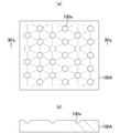
- 4 (a) and 4 (b) show the uneven shape formed on the surface of the graphite sheet according to the second embodiment of the present invention, FIG. 4 (a) is a plan view, and FIG. 4 (b).
- FIG. 1 is a sectional view showing a nitride semiconductor solar cell according to the first embodiment of the present invention.
- FIG. 2 shows an X-ray diffraction rocking curve in GaN growth on the graphite sheet according to the first embodiment of the present invention, and is
- FIG. 4 is a sectional view taken along line IVb-IVb in FIG.
- FIG. 5 is a cross-sectional view showing a nitride semiconductor solar cell according to a modification of the second embodiment of the present invention.
- 6 (a) to 6 (d) are cross-sectional views in order of steps showing a method for manufacturing a nitride semiconductor solar cell according to a modification of the second embodiment of the present invention.
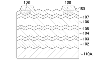
- the nitride semiconductor solar cell according to the first embodiment has an initial layer 101 made of, for example, aluminum nitride (AlN) having a thickness of about 20 nm on a graphite sheet 100 that is a flexible substrate.
- First semiconductor layer 102 including a pn junction made of indium gallium nitride (In 0.4 Ga 0.6 N), second contact layer 105 made of zinc oxide (ZnO), aluminum gallium nitride (Al 0.2)
- a third semiconductor layer 106 including a pn junction made of Ga 0.8 N) and a third contact layer 107 made of zinc oxide (ZnO) are sequentially formed by epitaxial growth.
- a back electrode 110 made of gold (Au) is formed on the surface of the graphite sheet 100 opposite to the initial layer 101.
- the third semiconductor layer 106 that receives the incident light mainly absorbs the incident light in the ultraviolet region and converts it into a photocurrent
- the second semiconductor layer 104 thereunder mainly receives the incident light in the blue-violet region. It absorbs and converts it into a photovoltaic current
- the first semiconductor layer 102 below it absorbs incident light mainly in the visible region and converts it into a photovoltaic current.
- the initial layer 101 made of AlN is formed on the main surface of the graphite sheet 100, for example, by metal organic chemical vapor deposition (Metal-Organic-Chemical-Vapor-Deposition). : MOCVD) method or pulsed laser deposition (PLD) method.
- MOCVD metal organic chemical vapor deposition
- PLD pulsed laser deposition
- FIG. 2 shows a rocking curve by X-ray diffraction when a GaN layer is formed on each initial layer 101 when AlN is used as the initial layer 101 on the graphite sheet 100 and when GaN is used. The result of having measured GaN (0002) peak is shown. Both layers use MOCVD for crystal growth. As can be seen from FIG. 2, the crystallinity of the GaN layer formed on the initial layer made of AlN is improved by using AlN as the initial layer.
- a first semiconductor layer made of In 0.4 Ga 0.6 N and including a pn junction is formed on the initial layer 101 made of AlN by MOCVD. 102 is formed. Subsequently, a low-resistance first contact layer 103 made of ZnO is formed by a PLD method. Thereafter, similarly, the second semiconductor layer 104 made of GaN and including a pn junction, the second contact layer 105 made of ZnO, and Al 0.2 Ga 0.8 N are formed on the first contact layer 103. A third semiconductor layer 106 including a pn junction and a third contact layer 107 made of ZnO are sequentially formed.
- magnesium (Mg) can be used as the p-type dopant for forming the p-type layer in the pn junction
- silicon (Si) is used as the n-type dopant for forming the n-type layer.
- Can do can do.
- the thickness of the first contact layer 103 and the second contact layer 105 needs to have sufficient transparency with respect to the wavelength absorbed by the pn junction located on the lower side. Therefore, the thickness of the contact layers 103 and 105 is preferably about 10 nm or less. In addition, the thickness of the third contact layer 107 formed on the top may be about 100 nm.
- the thicknesses of the first semiconductor layer 102, the second semiconductor layer 104, and the third semiconductor layer 106 may be about 0.5 ⁇ m, 0.3 ⁇ m, and 0.3 ⁇ m, respectively.
- each of the semiconductor layers 102, 104, and 106 is desirably a so-called pin-type junction in which an undoped layer is formed between the pn junctions. By increasing the amount of light absorbed by the undoped layer in the pin-type junction, the conversion efficiency of the solar cell can be improved.
- the thickness of each undoped layer that absorbs light at the pn junction constituting each of the semiconductor layers 102, 104, and 106 is preferably sufficiently thick so as not to increase the series resistance, for example, about 500 nm. .
- the contact layers 103, 105, and 107 made of ZnO have a larger forbidden band width than the semiconductor layers 102, 104, and 106 formed on the lower side, and thus absorb light. It is desirable to function as a transparent conductive film that is suppressed.
- magnesium (Mg), cadmium (Cd), or both of which can adjust the forbidden band width of ZnO may be added to ZnO constituting each contact layer 103, 105, 107.
- the first contact layer 103 is preferably made of Zn 0.8 Cd 0.2 O having a larger forbidden band width than In 0.4 Ga 0.6 N of the first semiconductor layer 102.
- the second contact layer 105 is preferably made of Zn 0.9 Mg 0.1 O having a larger forbidden band width than GaN, and the third contact layer 107 is made of Al 0.2 Ga 0.8 N. Zn 0.5 Mg 0.5 O having a larger forbidden band than that is desirable.
- the initial layer 101 and the semiconductor layers 102, 104, and 106 are provided above and below the first contact layer 103, above and below the second contact layer 105, and below the third contact layer 107.
- a diffusion suppression layer made of InAlGaN grown at a temperature lower than the growth temperature, and suppressing the diffusion of zinc (Zn) into each of the semiconductor layers 102, 104, and 106.
- the diffusion suppression layer provided on the upper and lower sides of the first contact layer 103 may have a thickness of 5 nm and a composition of AlN.
- the MOCVD method is used for the growth method of each semiconductor layer 102, 104, 106, and the PLD method is used for the growth method of each contact layer 103, 105, 107. Any one of them may be used.
- the growth method is limited to one type, a semiconductor layer or the like in the middle of growth is continuously grown without being exposed to the atmosphere, so that a natural oxide film or the like may be formed at the interface of the semiconductor layer or the like in the middle of the growth. Absent. Therefore, the nitride semiconductor solar cell according to the first embodiment can be formed without increasing the value of the series resistance.
- the first contact layer 103 made of a conductive oxide containing zinc (Zn) is replaced with the first semiconductor layer 102 made of a nitride semiconductor containing a pn junction.
- a second contact layer 105 is formed between the second semiconductor layer 104 and the second semiconductor layer 104, and a second contact layer 105 is formed between the second semiconductor layer 104 and the third semiconductor layer 106 each including a pn junction.
- the graphite sheet 100 ⁇ / b> A according to the second embodiment has a periodic uneven shape formed on its main surface.
- the initial layer 101 made of AlN and the first In 0.4 Ga 0.6 N made thereon are formed.
- Periodicity occurs in the formation of initial growth nuclei such as the semiconductor layer 102 of the semiconductor layer 102. This periodicity suppresses in-plane rotation of the crystal structure, and as a result, the crystallinity of each semiconductor layer 102, 104, etc. is further improved. For this reason, the highly efficient operation
- the first semiconductor layer 102 and the like including the pn junction includes so-called nonpolar surfaces including many surfaces other than the (0001) plane in the crystal plane. Become. For this reason, each of the semiconductor layers 102, 104, and 106 is not affected by the intrinsic polarization generated in the GaN-based semiconductor, so that the solar cell can operate with high efficiency. Further, since this uneven shape is also formed on the surface of the third contact layer 107 made of ZnO, the amount of incident light absorbed is increased, so that a more efficient solar cell can be realized.
- FIG. 4 (a) and FIG. 4 (b) show an example of a periodic uneven shape formed on the main surface of the graphite sheet 100A.
- a plurality of planar hexagonal recesses 100a are arranged to form hexagonal vertices.
- the length of one side of each recess 100a may be, for example, about 0.5 ⁇ m, and the interval between the placement of the recesses 100a may be about 20 ⁇ m.
- a resist pattern having the periodic recess 100a opened is formed on the main surface of the graphite sheet 100A by, for example, lithography, and the formed resist pattern is masked. Then, etching, for example, ashing in an oxidizing atmosphere may be performed.
- the graphite sheet 100 ⁇ / b> A and the initial layer 101 with the irregular shape formed on the main surface are removed, and the back electrode 110 ⁇ / b> A is the first semiconductor layer 102.
- the structure formed on the surface opposite to the first contact layer 102 in FIG. Note that gold (Au) can be used for the back electrode 110A.
- a periodic uneven shape is formed on the main surface of the graphite sheet 101a by the method described above.
- the initial layer 101 made of AlN, the first semiconductor layer 102 made of In 0.4 Ga 0.6 N, and ZnO A first contact layer 103 made of GaN, a second semiconductor layer 104 made of GaN, a second contact layer 105 made of ZnO, a third semiconductor layer 102 made of Al 0.2 Ga 0.8 N, and a second semiconductor layer made of ZnO.
- Three contact layers 107 are sequentially formed.
- the graphite sheet 101A is peeled from the formed GaN-based semiconductor layer. Since the graphite sheet 101A is flexible, it can be easily peeled off using an adhesive sheet or the like. Subsequently, the initial layer 101 exposed by peeling off the graphite sheet 101A is removed by dry etching using, for example, chlorine gas. Thereafter, a back electrode 110A made of Au is formed on the back surface of the first semiconductor layer 102 exposed by removing the initial layer 101 by vacuum vapor deposition or plating.
- the surface electrode 108 and the antireflection film 109 are formed on the third contact layer 107, thereby obtaining the nitride semiconductor solar cell shown in FIG.
- the number of stacked pn junctions is three, but the forbidden band width is gradually reduced from the upper layer toward the substrate side.
- Four or more semiconductor layers formed as described above may be stacked.
- the MOCVD method or the PLD method is used for the growth of the GaN-based semiconductor.
- the present invention is not limited to this, and other crystal growth methods such as a molecular beam epitaxy (MBE) method are used. May be.
- MBE molecular beam epitaxy
- the semiconductor layers and the contact layers may be continuously grown so that the interface between the layers does not deteriorate.
- a graphite sheet is used as a growth substrate for a GaN-based semiconductor
- the growth substrate is not limited to a graphite sheet, and for example, inexpensive silicon (Si) may be used.
- the nitride semiconductor solar cell includes a semiconductor layer 102 including a pn junction made of nitride semiconductors having different forbidden band widths on a low-cost and flexible graphite sheet 100.
- 104 and 106 are laminated, and contact layers 103, 105, and 107 made of, for example, ZnO are formed between the respective semiconductor layers.
- This pn junction is composed of, for example, In 0.4 Ga 0.6 N, GaN, and Al 0.2 Ga 0.8 N from the graphite sheet 100 side, and absorbs sunlight in the visible region, the blue-violet region, and the ultraviolet region, respectively. Thus, an electron hole pair is formed.
- the contact layer made of ZnO formed between the nitride semiconductor layers realizes a good ohmic contact with the semiconductor layers including pn junctions formed above and below and transmits incident light, the nitride semiconductor solar cell Enables high-efficiency operation.
- the nitride semiconductor solar cell according to the present invention can realize a good tandem structure and is useful for a thin-film nitride semiconductor solar cell that can be used for photovoltaic power generation.
Landscapes
- Photovoltaic Devices (AREA)
Abstract
L'invention porte sur une cellule solaire à semi-conducteur au nitrure comprenant une première couche semi-conductrice (102), qui comprend un semi-conducteur au nitrure d'éléments du groupe III et du groupe V et comprend une première jonction pn, et une seconde couche semi-conductrice (104), qui comprend un semi-conducteur au nitrure d'éléments du groupe III et du groupe V, diffère de la première couche semi-conductrice (102) en termes de bande interdite, et comprend une seconde jonction pn. Entre la première couche semi-conductrice (102) et la seconde couche semi-conductrice (104), une première couche de contact (103) a été formée en contact ohmique avec chacune de la première couche semi-conductrice (102) et de la seconde couche semi-conductrice (104), la première couche de contact (103) étant une couche d'oxyde contenant du zinc.
Applications Claiming Priority (2)
| Application Number | Priority Date | Filing Date | Title |
|---|---|---|---|
| JP2009-136984 | 2009-06-08 | ||
| JP2009136984A JP2010283255A (ja) | 2009-06-08 | 2009-06-08 | 窒化物半導体太陽電池 |
Publications (1)
| Publication Number | Publication Date |
|---|---|
| WO2010143342A1 true WO2010143342A1 (fr) | 2010-12-16 |
Family
ID=43308605
Family Applications (1)
| Application Number | Title | Priority Date | Filing Date |
|---|---|---|---|
| PCT/JP2010/001884 Ceased WO2010143342A1 (fr) | 2009-06-08 | 2010-03-16 | Cellule solaire à semi-conducteur au nitrure |
Country Status (2)
| Country | Link |
|---|---|
| JP (1) | JP2010283255A (fr) |
| WO (1) | WO2010143342A1 (fr) |
Cited By (1)
| Publication number | Priority date | Publication date | Assignee | Title |
|---|---|---|---|---|
| WO2013042525A1 (fr) * | 2011-09-21 | 2013-03-28 | ソニー株式会社 | Pile solaire multijonction, dispositif à semi-conducteurs composés, élément de conversion photoélectrique et structure stratifiée de couches à semi-conducteurs composés |
Citations (7)
| Publication number | Priority date | Publication date | Assignee | Title |
|---|---|---|---|---|
| JPS636882A (ja) * | 1986-06-26 | 1988-01-12 | ザ スタンダ−ド オイル カンパニ− | タンデム構成の光電池装置 |
| JPH02237172A (ja) * | 1989-03-10 | 1990-09-19 | Mitsubishi Electric Corp | 多層構造太陽電池 |
| JP2003152205A (ja) * | 2001-11-12 | 2003-05-23 | Sharp Corp | 光電変換素子及びその製造方法 |
| US20040118451A1 (en) * | 2002-05-24 | 2004-06-24 | Wladyslaw Walukiewicz | Broad spectrum solar cell |
| JP2004281938A (ja) * | 2003-03-18 | 2004-10-07 | Matsushita Electric Ind Co Ltd | 太陽電池およびその製造方法 |
| JP2005057251A (ja) * | 2003-07-24 | 2005-03-03 | Kyocera Corp | 多接合型半導体素子及びこれを用いた太陽電池素子 |
| JP2008235877A (ja) * | 2007-02-19 | 2008-10-02 | Showa Denko Kk | 太陽電池及びその製造方法 |
-
2009
- 2009-06-08 JP JP2009136984A patent/JP2010283255A/ja active Pending
-
2010
- 2010-03-16 WO PCT/JP2010/001884 patent/WO2010143342A1/fr not_active Ceased
Patent Citations (7)
| Publication number | Priority date | Publication date | Assignee | Title |
|---|---|---|---|---|
| JPS636882A (ja) * | 1986-06-26 | 1988-01-12 | ザ スタンダ−ド オイル カンパニ− | タンデム構成の光電池装置 |
| JPH02237172A (ja) * | 1989-03-10 | 1990-09-19 | Mitsubishi Electric Corp | 多層構造太陽電池 |
| JP2003152205A (ja) * | 2001-11-12 | 2003-05-23 | Sharp Corp | 光電変換素子及びその製造方法 |
| US20040118451A1 (en) * | 2002-05-24 | 2004-06-24 | Wladyslaw Walukiewicz | Broad spectrum solar cell |
| JP2004281938A (ja) * | 2003-03-18 | 2004-10-07 | Matsushita Electric Ind Co Ltd | 太陽電池およびその製造方法 |
| JP2005057251A (ja) * | 2003-07-24 | 2005-03-03 | Kyocera Corp | 多接合型半導体素子及びこれを用いた太陽電池素子 |
| JP2008235877A (ja) * | 2007-02-19 | 2008-10-02 | Showa Denko Kk | 太陽電池及びその製造方法 |
Cited By (1)
| Publication number | Priority date | Publication date | Assignee | Title |
|---|---|---|---|---|
| WO2013042525A1 (fr) * | 2011-09-21 | 2013-03-28 | ソニー株式会社 | Pile solaire multijonction, dispositif à semi-conducteurs composés, élément de conversion photoélectrique et structure stratifiée de couches à semi-conducteurs composés |
Also Published As
| Publication number | Publication date |
|---|---|
| JP2010283255A (ja) | 2010-12-16 |
Similar Documents
| Publication | Publication Date | Title |
|---|---|---|
| EP3611767B1 (fr) | Dispositifs optoélectroniques incluant une hétérojonction | |
| JP3657143B2 (ja) | 太陽電池及びその製造方法 | |
| US8367925B2 (en) | Light-electricity conversion device | |
| JP5538360B2 (ja) | 太陽電池の製造方法及び太陽電池 | |
| JP2020155778A (ja) | エピタキシャルリフトオフ後のウエハーの再利用のための犠牲エッチング保護層 | |
| CN102299158B (zh) | 单片集成太阳能模块和制造方法 | |
| US20120305059A1 (en) | Photon recycling in an optoelectronic device | |
| JP2008211217A (ja) | 薄膜型太陽電池及びその製造方法 | |
| US10388814B2 (en) | III-V solar cell structure with multi-layer back surface field | |
| Pouladi et al. | High‐efficiency flexible III‐V photovoltaic solar cells based on single‐crystal‐like thin films directly grown on metallic tapes | |
| JP2010267934A (ja) | 太陽電池およびその製造方法 | |
| US8431815B2 (en) | Photovoltaic device comprising compositionally graded intrinsic photoactive layer | |
| JP2010186915A (ja) | 太陽電池 | |
| KR101136882B1 (ko) | 질화물 반도체 기반의 태양전지 및 그 제조방법 | |
| JP5548878B2 (ja) | 多接合型光学素子 | |
| KR20120034964A (ko) | 기판, 상기 기판을 포함하는 태양 전지 및 이들의 제조 방법 | |
| KR101349484B1 (ko) | 태양전지 모듈 및 이의 제조방법 | |
| JP2010283408A (ja) | 太陽電池 | |
| WO2010143342A1 (fr) | Cellule solaire à semi-conducteur au nitrure | |
| KR101294770B1 (ko) | 양자점 태양전지 | |
| EP3300122A1 (fr) | Structure de materiau pour cellule solaire et cellule solaire la comprenant | |
| Lee et al. | High performance ultrathin GaAs solar cells | |
| JP5931653B2 (ja) | 光電変換素子 | |
| US20130160853A1 (en) | Solar cell having a pn hetero-junction | |
| US20120318337A1 (en) | Solar Cell |
Legal Events
| Date | Code | Title | Description |
|---|---|---|---|
| 121 | Ep: the epo has been informed by wipo that ep was designated in this application |
Ref document number: 10785874 Country of ref document: EP Kind code of ref document: A1 |
|
| NENP | Non-entry into the national phase |
Ref country code: DE |
|
| 122 | Ep: pct application non-entry in european phase |
Ref document number: 10785874 Country of ref document: EP Kind code of ref document: A1 |