WO2010143434A1 - Élément électroluminescent organique - Google Patents
Élément électroluminescent organique Download PDFInfo
- Publication number
- WO2010143434A1 WO2010143434A1 PCT/JP2010/003869 JP2010003869W WO2010143434A1 WO 2010143434 A1 WO2010143434 A1 WO 2010143434A1 JP 2010003869 W JP2010003869 W JP 2010003869W WO 2010143434 A1 WO2010143434 A1 WO 2010143434A1
- Authority
- WO
- WIPO (PCT)
- Prior art keywords
- emitting layer
- light emitting
- host
- electron transport
- layer
- Prior art date
- Legal status (The legal status is an assumption and is not a legal conclusion. Google has not performed a legal analysis and makes no representation as to the accuracy of the status listed.)
- Ceased
Links
Images


Classifications
-
- H—ELECTRICITY
- H10—SEMICONDUCTOR DEVICES; ELECTRIC SOLID-STATE DEVICES NOT OTHERWISE PROVIDED FOR
- H10K—ORGANIC ELECTRIC SOLID-STATE DEVICES
- H10K50/00—Organic light-emitting devices
- H10K50/10—OLEDs or polymer light-emitting diodes [PLED]
- H10K50/14—Carrier transporting layers
-
- H—ELECTRICITY
- H10—SEMICONDUCTOR DEVICES; ELECTRIC SOLID-STATE DEVICES NOT OTHERWISE PROVIDED FOR
- H10K—ORGANIC ELECTRIC SOLID-STATE DEVICES
- H10K50/00—Organic light-emitting devices
- H10K50/10—OLEDs or polymer light-emitting diodes [PLED]
- H10K50/11—OLEDs or polymer light-emitting diodes [PLED] characterised by the electroluminescent [EL] layers
-
- H—ELECTRICITY
- H10—SEMICONDUCTOR DEVICES; ELECTRIC SOLID-STATE DEVICES NOT OTHERWISE PROVIDED FOR
- H10K—ORGANIC ELECTRIC SOLID-STATE DEVICES
- H10K50/00—Organic light-emitting devices
- H10K50/10—OLEDs or polymer light-emitting diodes [PLED]
- H10K50/11—OLEDs or polymer light-emitting diodes [PLED] characterised by the electroluminescent [EL] layers
- H10K50/125—OLEDs or polymer light-emitting diodes [PLED] characterised by the electroluminescent [EL] layers specially adapted for multicolour light emission, e.g. for emitting white light
-
- H—ELECTRICITY
- H10—SEMICONDUCTOR DEVICES; ELECTRIC SOLID-STATE DEVICES NOT OTHERWISE PROVIDED FOR
- H10K—ORGANIC ELECTRIC SOLID-STATE DEVICES
- H10K50/00—Organic light-emitting devices
- H10K50/10—OLEDs or polymer light-emitting diodes [PLED]
- H10K50/14—Carrier transporting layers
- H10K50/16—Electron transporting layers
-
- H—ELECTRICITY
- H10—SEMICONDUCTOR DEVICES; ELECTRIC SOLID-STATE DEVICES NOT OTHERWISE PROVIDED FOR
- H10K—ORGANIC ELECTRIC SOLID-STATE DEVICES
- H10K59/00—Integrated devices, or assemblies of multiple devices, comprising at least one organic light-emitting element covered by group H10K50/00
- H10K59/30—Devices specially adapted for multicolour light emission
- H10K59/35—Devices specially adapted for multicolour light emission comprising red-green-blue [RGB] subpixels
-
- H—ELECTRICITY
- H10—SEMICONDUCTOR DEVICES; ELECTRIC SOLID-STATE DEVICES NOT OTHERWISE PROVIDED FOR
- H10K—ORGANIC ELECTRIC SOLID-STATE DEVICES
- H10K85/00—Organic materials used in the body or electrodes of devices covered by this subclass
- H10K85/30—Coordination compounds
- H10K85/321—Metal complexes comprising a group IIIA element, e.g. Tris (8-hydroxyquinoline) gallium [Gaq3]
- H10K85/324—Metal complexes comprising a group IIIA element, e.g. Tris (8-hydroxyquinoline) gallium [Gaq3] comprising aluminium, e.g. Alq3
-
- H—ELECTRICITY
- H10—SEMICONDUCTOR DEVICES; ELECTRIC SOLID-STATE DEVICES NOT OTHERWISE PROVIDED FOR
- H10K—ORGANIC ELECTRIC SOLID-STATE DEVICES
- H10K85/00—Organic materials used in the body or electrodes of devices covered by this subclass
- H10K85/30—Coordination compounds
- H10K85/341—Transition metal complexes, e.g. Ru(II)polypyridine complexes
- H10K85/342—Transition metal complexes, e.g. Ru(II)polypyridine complexes comprising iridium
-
- H—ELECTRICITY
- H10—SEMICONDUCTOR DEVICES; ELECTRIC SOLID-STATE DEVICES NOT OTHERWISE PROVIDED FOR
- H10K—ORGANIC ELECTRIC SOLID-STATE DEVICES
- H10K85/00—Organic materials used in the body or electrodes of devices covered by this subclass
- H10K85/60—Organic compounds having low molecular weight
- H10K85/615—Polycyclic condensed aromatic hydrocarbons, e.g. anthracene
- H10K85/626—Polycyclic condensed aromatic hydrocarbons, e.g. anthracene containing more than one polycyclic condensed aromatic rings, e.g. bis-anthracene
-
- H—ELECTRICITY
- H10—SEMICONDUCTOR DEVICES; ELECTRIC SOLID-STATE DEVICES NOT OTHERWISE PROVIDED FOR
- H10K—ORGANIC ELECTRIC SOLID-STATE DEVICES
- H10K85/00—Organic materials used in the body or electrodes of devices covered by this subclass
- H10K85/60—Organic compounds having low molecular weight
- H10K85/631—Amine compounds having at least two aryl rest on at least one amine-nitrogen atom, e.g. triphenylamine
- H10K85/633—Amine compounds having at least two aryl rest on at least one amine-nitrogen atom, e.g. triphenylamine comprising polycyclic condensed aromatic hydrocarbons as substituents on the nitrogen atom
-
- H—ELECTRICITY
- H10—SEMICONDUCTOR DEVICES; ELECTRIC SOLID-STATE DEVICES NOT OTHERWISE PROVIDED FOR
- H10K—ORGANIC ELECTRIC SOLID-STATE DEVICES
- H10K2101/00—Properties of the organic materials covered by group H10K85/00
- H10K2101/30—Highest occupied molecular orbital [HOMO], lowest unoccupied molecular orbital [LUMO] or Fermi energy values
Definitions
- the present invention relates to an organic electroluminescence (EL) element, particularly a highly efficient organic EL element.
- EL organic electroluminescence
- organic EL elements When organic EL elements are classified according to their light emission principles, they can be divided into two types: fluorescent and phosphorescent types.
- fluorescent and phosphorescent types When a voltage is applied to the organic EL element, holes are injected from the anode and electrons are injected from the cathode, and these recombine in the light emitting layer to form excitons.
- the formed excitons become singlet excitons and triplet excitons according to the statistical rule of electron spin, which are generated at a ratio of 25%: 75%. For this reason, it is said that the internal quantum efficiency of fluorescence emission by singlet excitons is limited to 25%.
- a fluorescent element using a fluorescent material has recently been developed with a long-life technology and is being applied to a full-color display such as a mobile phone or a television. However, high efficiency has been a problem.
- Non-Patent Document 1 a non-doped element using an anthracene compound as a host material is analyzed, and as a mechanism, singlet excitons are generated by collisional fusion of two triplet excitons. Fluorescence emission is increasing.
- Non-Patent Document 1 only discloses that an increase in fluorescence emission is confirmed by collisional fusion of triplet excitons in a non-doped element composed of only a host material. The increase was as low as 3-6%.
- Non-Patent Document 2 reports that the blue quantum element has an internal quantum efficiency of 28.5%, which exceeds the conventional theoretical limit of 25%. However, no technical means for exceeding 25% has been disclosed, and further higher efficiency has been demanded from the viewpoint of practical use of a full-color organic EL television.
- Patent Document 1 Another example using triplet excitons in a fluorescent element is disclosed in Patent Document 1.
- the lowest triplet excited state (T1) is lower than the lowest singlet excited state (S1), but the higher triplet excited state (T2) may be higher than S1.
- the external quantum efficiency is about 6% (when the light extraction efficiency is 25%, the internal quantum efficiency is 24%), which does not exceed the limit value of 25% that has been conventionally known.
- the mechanism here is due to intersystem crossing from a triplet excited state to a singlet excited state in one molecule, and the two triplet excitons disclosed in Non-Patent Document 1 The singlet generation phenomenon due to the collision has not occurred.
- phenanthroline derivatives such as BCP (Bathocuproin) and BPhen are used for the hole blocking layer in the fluorescent element, thereby increasing the density of holes at the interface between the hole blocking layer and the light emitting layer, and efficiently. Techniques for causing recombination are disclosed.
- phenanthroline derivatives such as BCP (basocuproin) and BPhen are vulnerable to holes, have poor oxidation durability, and have insufficient performance from the viewpoint of extending the lifetime of the device.
- Patent Documents 4 and 5 disclose examples in which an aromatic compound such as an anthracene derivative is used as a material for an electron transport layer in contact with a light emitting layer in a fluorescent element.
- an aromatic compound such as an anthracene derivative
- the triplet energy of the electron transport layer normally designed in so-called phosphorescent devices.
- the triplet energy of the electron transport layer is smaller than the triplet energy of the light-emitting layer, so that triplet excitons generated in the light-emitting layer are actually transported by electrons. It has been diffused to the layer and then undergoes a thermal deactivation process, and it has been difficult to exceed 25%, which is the theoretical limit value of conventional fluorescence.
- Patent Document 6 discloses a device using a fluoranthene dopant exhibiting long-life and high-efficiency blue light emission, but it is not necessarily high-efficiency.
- the phosphorescent type uses light emitted directly from triplet excitons. Since singlet excitons are also converted into triplet excitons by spin conversion inside the light emitting molecule, in principle, it is expected that an internal luminous efficiency of nearly 100% can be obtained. Therefore, since a phosphorescent light emitting device using an Ir complex was announced by Forrest et al. In 2000, a phosphorescent light emitting device has attracted attention as a technique for improving the efficiency of organic EL devices. However, although red phosphorescent devices have reached the practical application range, green and blue phosphorescent devices have a shorter lifetime than fluorescent-type devices, and in particular, blue phosphorescence has insufficient color purity and luminous efficiency. The current situation is that it has not been put into practical use.
- the light emitting layer is separately coated with a blue fluorescent light emitting layer, a green phosphorescent light emitting layer, and a red phosphorescent light emitting layer.
- the manufacturing process is reduced and mass production is facilitated.
- the blue fluorescent light-emitting layer, the green phosphorescent light-emitting layer, and the red phosphorescent light-emitting layer have greatly different physical property values such as affinity, ionization potential, and energy gap. Therefore, when the peripheral layer is a common layer, the green phosphorescent light emitting layer with the largest energy gap is designed to optimize the carrier injection property, and the performance of other light emitting layers (especially the blue fluorescent light emitting layer) The decline was happening.
- a light emitting layer is composed of a blue light emitting layer containing a fluorescent light emitting dopant, a green light emitting layer containing a phosphorescent light emitting dopant, and a red light emitting layer containing a phosphorescent light emitting dopant, and the hole suppressing layer is a common layer.
- the element provided as is described.
- the manufacturing process is reduced by using the hole suppression layer as a common layer, electron injection from the hole barrier layer to each light emitting layer has become a problem by using the hole suppression layer as a common layer.
- the difference in affinity between the blue light-emitting layer and the hole-inhibiting layer is as small as about 0.2 eV.
- the green light-emitting layer uses a material with low affinity such as CBP, the affinity with the hole-inhibiting layer. The difference is large, about 0.6 eV. For this reason, the electron injection property is lowered in the green light emitting layer, and the drive voltage is increased. Furthermore, since the coupling region is concentrated at the interface between the green phosphorescent light emitting layer and the hole suppressing layer, exciton diffusion is large and the light emitting efficiency of the green light emitting layer does not increase.
- Patent Document 10 discloses an organic EL element in which an affinity difference ⁇ Af between a light-emitting layer containing a phosphorescent dopant and an electron transport layer is 0.2 ⁇ Af ⁇ 0.65 eV. However, when the blue light emitting layer, the green light emitting layer, and the red light emitting layer are separately applied, no disclosure is made regarding the efficiency of the light emitting layer.
- Triplet-Triplet Fusion TTF phenomenon
- the triplet excitons are confined in the light emitting layer, and the TTF phenomenon occurs. As a result, the fluorescent element is realized with high efficiency and long life.
- the electron injection property is improved, and the blue fluorescent light-emitting layer, green phosphorescent light-emitting layer, and red
- the relationship between the materials used for the electron transport layer provided in common with the phosphorescent light-emitting layer has been found, and high efficiency of the full-color element has been realized.
- JP-T-2002-525808 discloses a technique for improving efficiency by providing a barrier layer made of BCP (basocuproin) which is a phenanthroline derivative so as to be adjacent to the light emitting layer, and confining holes and excitons. Yes.
- BCP basic polypeptide
- a specific aromatic ring compound is used for a hole blocking layer to achieve high efficiency and long life.
- TTA triplet-triplet annihilation
- An object of the present invention is to improve efficiency and lifetime without increasing the manufacturing cost in an organic EL device having a blue light emitting layer, a green light emitting layer, and a red light emitting layer.
- the following organic EL elements are provided. 1. Between the anode and cathode facing each other, from the anode side, a hole transport zone, a light emitting layer and an electron transport zone are provided in this order, The light emitting layer is formed of a red light emitting layer, a green light emitting layer and a blue light emitting layer, The blue light emitting layer includes a host BH and a fluorescent light emitting dopant FBD, The triplet energy E T fbd of the fluorescent luminescent dopant FBD is greater than the triplet energy E T bh of the host BH; The green light emitting layer includes a host GH and a phosphorescent dopant PGD, In said electron transporting zone, the red light emitting layer, a common electron transport layer adjacent to the green light emitting layer and the blue light emitting layer is provided, the triplet energy E T el of the material constituting the electron transport layer is E Greater than T bh , The difference in affinity between the host a host BH and
- the red light emitting layer includes a host RH and a phosphorescent dopant PRD, 2.
- the organic electroluminescence device according to any one of 1 to 4, wherein an electron injection layer is provided between the electron transport layer and the cathode in the electron transport zone. 6).
- the organic electroluminescence device according to any one of 1 to 5, wherein the host GH has an affinity Af gh of 2.6 eV or more. 7).
- the organic electroluminescence device according to any one of 1 to 6, wherein an ionization potential Ip gd of the dopant GD is 5.2 eV or more. 8).
- the organic electroluminescence device according to any one of 1 to 7, wherein a second dopant is included in at least one of the blue light emitting layer, the green light emitting layer, and the red light emitting layer. 9.
- the efficiency and life can be improved without increasing the manufacturing cost.
- FIG. 1 is a diagram showing a configuration of an organic EL element according to an embodiment of the present invention.
- the organic EL element 1 includes a hole transport zone 20, a light emitting layer 30, and an electron transport zone 40 in this order from the anode 10 side between the anode 10 and the cathode 50 facing each other on the substrate 60.
- the light emitting layer 30 is formed of a blue light emitting layer 32, a green light emitting layer 34 and a red light emitting layer 36.
- the light emitting layer 30 is provided with a red light emitting layer 36, a green light emitting layer 34, and a blue light emitting layer 32 juxtaposed in a direction perpendicular to the substrate surface.
- the blue light emitting layer 32 includes a host BH and a fluorescent light emitting dopant FBD
- the green light emitting layer 34 includes a host GH and a phosphorescent light emitting dopant PGD
- the red light emitting layer 36 includes a host RH and phosphorescent light emitting material.
- a dopant PRD a common electron transport layer 42 is provided in the electron transport zone 40 adjacent to the blue light emitting layer 32, the green light emitting layer 34 and the red light emitting layer 36.
- An electron injection layer 44 is preferably provided in the electron transport zone 40 and between the electron transport layer 42 and the cathode 50, more preferably adjacent to the electron transport layer 42.
- a hole transport layer or a hole transport layer and a hole injection layer can be provided.
- the anode 10 is laminated on the substrate 60 and patterned.
- the anode 10 uses a metal film which is a reflective film in the case of a front light emitting structure, and indium tin oxide (ITO) or indium zinc oxide which is a transparent electrode in the case of a back light emitting structure.
- ITO indium tin oxide
- ITO indium zinc oxide
- a hole transport zone 20 a hole injection layer is laminated over the entire surface of the substrate, and a hole transport layer is further laminated thereon. Each light emitting layer is formed so as to correspond to the position of the anode.
- the blue light emitting layer 32, the green light emitting layer 34, and the red light emitting layer 36 are finely patterned using a shadow mask.
- the electron transport zone 40 is laminated over the entire surface of the blue light emitting layer 32, the green light emitting layer 34 and the red light emitting layer 36.
- a cathode is laminated to complete an organic EL element.
- the substrate a glass substrate, a TFT substrate, or the like can be used.
- the hole transport zone 20 is provided in common using a common material as the hole injection layer and the hole transport layer, but the blue light emitting layer 32, the green light emitting layer 34, and the red light emitting layer are provided.
- different materials may be provided by micropatterning.
- the hole transporting zone may be a single hole transporting layer, or two or more layers may be laminated by a combination of a hole injection layer and a hole transporting layer.
- some layers are provided in common, and the other layers correspond to the blue light emitting layer 32, the green light emitting layer 34, and the red light emitting layer 36, and different materials are used. It may be provided by forming a fine pattern.
- the light emitting layer of the organic EL element of the present invention includes a blue pixel, a green pixel, and a red pixel.
- the blue pixel is from the blue light emitting layer
- the green pixel is from the green light emitting layer
- the red pixel is from the red light emitting layer. Composed.
- a voltage is applied to each pixel independently. Therefore, in the organic EL element 1 of FIG. 1, the blue light emitting layer 32, the green light emitting layer 34, and the red light emitting layer 36 do not always emit light at the same time, but the three light emitting layers 32, 34, 36 are selectively made to emit light, respectively. be able to.
- the organic EL element of the present embodiment includes one blue pixel, one green pixel, and one red pixel, but may be repeated with these as one unit. Also, there may be a plurality of each pixel. For example, the repetition may be a single unit composed of one blue pixel, two green pixels, and one red pixel.
- the organic EL element of the present invention has a phenomenon described in Non-Patent Document 1, that is, a phenomenon in which singlet excitons are generated by collisional fusion of two triplet excitons (hereinafter, referred to as “blue light emitting layer 32”).
- Triplet-Triplet-Fusion TTF phenomenon).
- the TTF phenomenon will be described below. Holes and electrons injected from the anode and cathode recombine in the light emitting layer to generate excitons.
- the spin state has a ratio of 25% for singlet excitons and 75% for triplet excitons, as is conventionally known.
- TTF ratio TTF-derived emission ratio
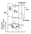
- FIG. 2 is a schematic diagram showing an example of the energy level of the blue light emitting layer of the organic EL element shown in FIG.
- the upper diagram of FIG. 2 shows the device configuration and the HOMO and LUMO energy levels of each layer (the LUMO energy level may be referred to as affinity (Af), and the HOMO energy level may be referred to as ionization potential (Ip)).
- the following diagram schematically shows the lowest excited singlet energy level and the lowest excited triplet energy level of each layer.
- the triplet energy is the difference between the energy in the lowest excited triplet state and the energy in the ground state
- the singlet energy (sometimes referred to as an energy gap) is the lowest excited singlet state. The difference between energy and ground state energy.
- Holes injected from the anode are injected into the light emitting layer through the hole transport zone, and electrons injected from the cathode are injected into the light emitting layer through the electron transport zone. Thereafter, holes and electrons are recombined in the light emitting layer, and singlet excitons and triplet excitons are generated. There are two ways in which recombination occurs on the host molecule and on the dopant molecule. As shown in the lower diagram of FIG. 2, when the triplet energies of the host and dopant of the blue light emitting layer are E T h and E T d , respectively, the relationship of E T h ⁇ E T d is satisfied.
- triplet excitons generated by recombination on the host do not move to a dopant having a higher triplet energy. Further, triplet excitons generated by recombination on the dopant molecule quickly transfer energy to the host molecule. That is, triplet excitons collide with each other on the host efficiently by the TTF phenomenon without the triplet excitons of the host moving to the dopant, so that singlet excitons are generated. Furthermore, since the singlet energy E S d of the dopant is smaller than the singlet energy E S h of the host, singlet excitons generated by the TTF phenomenon transfer energy from the host to the dopant, and the fluorescence of the dopant. Contributes to light emission.
- the electron transport layer prevents triplet excitons generated in the blue light-emitting layer from diffusing into the electron transport band, and confines the triplet excitons in the blue light-emitting layer. It has the function of increasing the child density and causing the TTF phenomenon efficiently.
- triplet energy E T el of the electron transport layer is greater than E T h, further preferably larger than E T d. Since the electron transport layer prevents the triplet excitons from diffusing into the electron transport band, the host triplet excitons efficiently become singlet excitons in the blue light-emitting layer, and the singlet excitons thereof. The child moves onto the dopant and optically deactivates.
- the hole transport layer in the hole transport zone, is adjacent to the blue light-emitting layer, and the triplet energy E T ho of the hole transport layer is expressed as the E T of the host of the blue light-emitting layer.
- E T ho of the hole transport layer is expressed as the E T of the host of the blue light-emitting layer.
- the difference in affinity between the host GH of the green light emitting layer and the material constituting the electron transport layer is within 0.4 eV.
- the triplet energy of the phosphorescent dopant PGD green emitting layer is greater than the triplet energy E T el of the material constituting the electron transport layer. Therefore, it is preferable that the triplet energy E T el of the material forming the electron-transporting layer larger than the triplet energy of the phosphorescent dopant PGD.
- an electron transport material having a large triplet energy has problems in electron injection from an electrode and hole durability. In order to obtain an optimum phosphorescent device, an electron transport material having a large triplet energy.
- triplet excitons on the phosphorescent dopant PGD are transferred to a material constituting an electron transport layer having a smaller triplet energy before phosphorescence emission, and the light emission efficiency of the green light emission layer is lowered. . Therefore, as in the present invention, when the difference in affinity between the host GH of the green light emitting layer and the material constituting the electron transporting layer is within 0.4 eV, the electron injection property from the electron transporting layer to the green light emitting layer is improved. Electrons and holes are recombined with bias toward the hole transport band side of the light emitting layer, that is, away from the electron transport band.
- the hole mobility ⁇ h and the electron mobility ⁇ e of the host of the light emitting layer are preferably ⁇ e / ⁇ h> 1. Particularly preferably, ⁇ e / ⁇ h> 5.
- the light emitting layers of three colors are formed in parallel, but mass productivity is improved by using a common material as the electron transport layer.
- the blue light emitting layer uses the TTF phenomenon to increase the light emitting efficiency of the blue light emitting layer, and the green light emitting layer adjusts the affinity to prevent the light emitting efficiency of the green light emitting layer from being lowered, so Both have achieved high efficiency.
- the red light emitting layer 36 can be configured to include the host RH and the phosphorescent dopant PRD.
- the difference in affinity between the host RH and the material constituting the electron transport layer is preferably within 0.4 eV. This is because, as described above, it is difficult to transfer triplet energy from the red light emitting layer to the electron transporting layer to prevent a decrease in light emission efficiency.
- the difference in affinity between the host BH of the blue light emitting layer and the material constituting the electron transport layer is within 0.4 eV. This is because the electron injection property to the light emitting layer is improved by setting the difference in affinity within 0.4 eV.
- the electron injecting property to the light emitting layer is lowered, the density of triplet excitons is reduced by reducing electron-hole recombination in the light emitting layer.
- the collision frequency of triplet excitons decreases and the TTF phenomenon does not occur efficiently.
- the voltage can be lowered by improving the electron injection.
- the host GH preferably has an affinity Af gh of 2.6 eV or more in order to increase the inflow of electrons and separate the recombination region from the electron transport band.
- the ionization potential Ip gd of the dopant GD of the green light emitting layer is preferably 5.2 eV or more in order to improve the recombination probability.
- the green light emitting layer preferably includes a second dopant GD2 having an affinity Af gd2 having a difference from the affinity Af gh of the host GH within 0.4 eV . Furthermore, it is desirable that the energy gap of the dopant PGD is smaller than the energy gap of the second dopant GD2.
- electrons typically move from the electron transport layer to the host GH of the green light emitting layer, and then from the host GH to the dopant PGD.
- the difference between the affinity Af gh of the host GH and the affinity Af gd of the dopant increases and the electron injectability into the dopant decreases, a part of the electrons flows in the anode direction as it is without moving from the host GH to the dopant PGD. There is a case.
- the electrons are transferred from the electron transport layer to the host GH of the green light emitting layer, then the second dopant GD2, and the dopant PGD. It is possible to prevent some of the electrons from flowing to the anode without moving to the dopant PGD. Therefore, more electrons reach the dopant PGD and the recombination probability is improved, resulting in an increase in luminous efficiency.
- the blue light-emitting layer and the red light-emitting layer may also contain the second dopant having an affinity Af gd2 having a difference from the host affinity Af gh of 0.4 eV or less as described above.
- the second dopant By including the second dopant, it is possible to prevent electrons from flowing in the anode direction without moving to the dopant.
- the blue light-emitting layer, the green light-emitting layer, the host of the red light-emitting layer, the dopant, and the material constituting the electron transport layer are selected from known compounds, and the compounds satisfying the above-described conditions necessary for the present invention or suitable conditions. It can manufacture by selecting.
- the material of each layer is not limited as long as the conditions necessary for the present invention are satisfied, but is preferably selected from the following compounds.
- the host of the blue light emitting layer is an anthracene derivative, a polycyclic aromatic skeleton-containing compound or the like, preferably an anthracene derivative.
- the dopant of the blue light emitting layer is fluoranthene derivative, pyrene derivative, arylacetylene derivative, fluorene derivative, boron complex, perylene derivative, oxadiazole derivative, anthracene derivative, etc., preferably fluoranthene derivative, pyrene derivative, boron complex, more preferably Fluoranthene derivatives and boron complex compounds.
- the host is an anthracene derivative and the dopant is a fluoranthene derivative or a boron complex.
- X 1 to X 12 are hydrogen or a substituent.
- X 1 to X 2 , X 4 to X 6 and X 8 to X 11 are hydrogen atoms
- X 3 , X 7 and X 12 are substituted or unsubstituted aryl groups having 5 to 50 ring atoms. It is a compound which is.
- X 1 to X 2 , X 4 to X 6 and X 8 to X 11 are hydrogen atoms, and X 7 and X 12 are substituted or unsubstituted aryl groups having 5 to 50 ring atoms, X A compound in which 3 is —Ar 1 —Ar 2 (Ar 1 is a substituted or unsubstituted arylene group having 5 to 50 ring atoms, Ar 2 is a substituted or unsubstituted aryl group having 5 to 50 ring atoms) It is.
- X 1 to X 2 , X 4 to X 6 and X 8 to X 11 are hydrogen atoms, and X 7 and X 12 are substituted or unsubstituted aryl groups having 5 to 50 ring atoms,
- X 3 is —Ar 1 —Ar 2 —Ar 3 (Ar 1 and Ar 2 are each a substituted or unsubstituted arylene group having 5 to 50 ring atoms; Ar 3 is a substituted or unsubstituted ring atom number 5; ⁇ 50 aryl groups).
- a and A ′ represent an independent azine ring system corresponding to a 6-membered aromatic ring system containing at least one nitrogen
- X a and X b are each independently a substituent
- a and Xb may be linked to ring A and ring A ′, respectively, to form a fused ring with ring A and ring A ′, wherein the fused ring contains an aryl or heteroaryl substituent
- m and n each independently represents 0-4
- Z a and Z b each independently represent a halide, and 1, 2, 3, 4, 1 ′, 2 ′, 3 ′ and 4 ′.
- the azine ring is such that 1, 2, 3, 4, 1 ′, 2 ′, 3 ′ and 4 ′ are all carbon atoms, m and n are 2 or more, and X a and X b are It is a quinolinyl or isoquinolinyl ring which represents a substituent having 2 or more carbon atoms that are linked to form an aromatic ring.
- Z a and Z b are preferably fluorine atoms.
- Ar 001 is a substituted or unsubstituted condensed aromatic group having 10 to 50 ring carbon atoms.
- Ar 002 is a substituted or unsubstituted aromatic group having 6 to 50 ring carbon atoms.
- X 001 to X 003 are each independently a substituted or unsubstituted aromatic group having 6 to 50 ring carbon atoms, a substituted or unsubstituted aromatic heterocyclic group having 5 to 50 ring atoms, substituted or unsubstituted An alkyl group having 1 to 50 carbon atoms, a substituted or unsubstituted alkoxy group having 1 to 50 carbon atoms, a substituted or unsubstituted aralkyl group having 6 to 50 carbon atoms, a substituted or unsubstituted ring atom having 5 to 50 ring atoms.
- a, b and c are each an integer of 0 to 4.
- n is an integer of 1 to 3. When n is 2 or more, the numbers in [] may be the same or different.
- n is 1.
- a, b and c are 0.
- the fluorescent light-emitting dopant of the blue light-emitting layer is preferably a compound represented by the following formula.
- Ar 1 to Ar 6 are each an aryl group having 6 to 30 carbon atoms
- Ar 7 is an arylene group having 6 to 30 carbon atoms.
- Ar 1 to Ar 7 may be substituted, and the substituent is preferably an alkoxy group, a dialkylamino group, an alkyl group, a fluoroalkyl group, or a silyl group.
- m is 0 or 1
- n is 0 or 1.
- L 1 and L 2 are each an alkenylene group or a divalent aromatic hydrocarbon group.
- a dibenzofuran compound described in WO05 / 113531, JP2005-314239, a fluorene compound described in WO02 / 14244, and a benzanthracene compound described in WO08 / 145239 can also be used.
- JP2004-204238, WO05 / 108348, WO04 / 83162, WO09 / 845122, KR10-2008-79958, KR10-2007-115588, KR10-2010-24894, pyrene compounds described in WO04 / 44088 And anthracene compounds described in WO07 / 21117 can also be used.
- the host is preferably a compound in which a cyclic structure or a single atom is bonded to each other (including a ring structure and a single atom bond), and the bond is a single bond.
- Unpreferable examples include compounds having a carbon-carbon double bond other than a cyclic structure. This is because the triplet exciton energy generated on the host is not used for the TTF phenomenon and is consumed for the structural change of the double bond.
- the host of the green light emitting layer is preferably a compound represented by the following formula (1) or (2).
- Ar 6 , Ar 7 and Ar 8 are each independently a substituted or unsubstituted aromatic hydrocarbon group having 6 to 24 ring carbon atoms, or a substituted or unsubstituted group. Represents an aromatic heterocyclic group having 3 to 24 ring atoms.
- Ar 6 , Ar 7 and Ar 8 may have one or a plurality of substituents Y, and when there are a plurality of them, they may be the same or different, and Y is an alkyl group having 1 to 20 carbon atoms.
- X 1 , X 2 , X 3 and X 4 each independently represent O, S, N—R 1 or CR 2 R 3 , and o, p and q are 0 Or 1, s represents 1, 2 or 3.
- R 1 , R 2 and R 3 are each independently an alkyl group having 1 to 20 carbon atoms, a substituted or unsubstituted cycloalkyl group having 3 to 20 ring carbon atoms, or an aralkyl having 7 to 24 carbon atoms.
- L 1 is a single bond, an alkylene group having 1 to 20 carbon atoms, a substituted or unsubstituted cycloalkylene group having 3 to 20 ring carbon atoms, or a divalent group having 2 to 20 carbon atoms.
- L 2 is a single bond, an alkylene group having 1 to 20 carbon atoms, a substituted or unsubstituted cycloalkylene group having 3 to 20 ring carbon atoms, a divalent silyl group having 2 to 20 carbon atoms, A substituted or unsubstituted divalent aromatic hydrocarbon group having 6 to 24 ring carbon atoms, or a substituted or unsubstituted divalent aromatic group having 3 to 24 ring atoms and linked to Ar 8 by a carbon-carbon bond Represents a heterocyclic group.
- n represents 2, 3 or 4, and each forms a dimer, trimer or tetramer with L 3 as a linking group.
- L 3 is a single bond, an alkylene group having 1 to 20 carbon atoms, a substituted or unsubstituted cycloalkylene group having 3 to 20 ring carbon atoms, or 2 to 20 carbon atoms.
- a 1 represents a hydrogen atom, a substituted or unsubstituted cycloalkyl group having 3 to 20 ring carbon atoms, a silyl group having 3 to 20 carbon atoms, a substituted or unsubstituted ring formation. It represents an aromatic hydrocarbon group having 6 to 24 carbon atoms, or a substituted or unsubstituted aromatic heterocyclic group having 3 to 24 ring atoms and linked to L 1 by a carbon-carbon bond.
- a 2 is a hydrogen atom, a substituted or unsubstituted cycloalkyl group having 3 to 20 ring carbon atoms, a silyl group having 3 to 20 carbon atoms, a substituted or unsubstituted ring carbon number 6 to 24 represents an aromatic hydrocarbon group, or a substituted or unsubstituted aromatic heterocyclic group having 3 to 24 ring-forming atoms and linked to L 2 by a carbon-carbon bond.
- the host of the green light emitting layer is preferably a compound represented by the following general formula (3) or (4).
- (Cz-) n A (3) Cz (-A) m (4) [Wherein, Cz is a substituted or unsubstituted arylcarbazoyl group or carbazoylalkylene group, and A is a group represented by the following general formula.
- n and m are each an integer of 1 to 3.
- M and M ′ are each independently a nitrogen-containing heteroaromatic ring having 2 to 40 carbon atoms that forms a substituted or unsubstituted ring, and may be the same or different.
- L is a single bond or a substituted ring.
- an unsubstituted arylene group having 6 to 30 carbon atoms a substituted or unsubstituted cycloalkylene group having 5 to 30 carbon atoms, and a substituted or unsubstituted heteroaromatic ring having 2 to 30 carbon atoms, p being 0 to 2
- q is an integer from 1 to 2
- r is an integer from 0 to 2, provided that p + r is 1 or more.
- the phosphorescent dopant of the green light-emitting layer preferably contains a metal complex composed of a metal selected from the group consisting of Ir, Pt, Os, Au, Cu, Re, and Ru and a ligand.
- a metal complex composed of a metal selected from the group consisting of Ir, Pt, Os, Au, Cu, Re, and Ru and a ligand.
- Specific examples of such a dopant material include, for example, PQIr (iridium (III) bis (2-phenylquinolyl-N, C 2 ′ ) acetylacetonate), Ir (ppy) 3 (fac-tris (2-phenylpyridine) iridium).
- PQIr iridium (III) bis (2-phenylquinolyl-N, C 2 ′ ) acetylacetonate
- Ir (ppy) 3 fac-tris (2-phenylpyridine) iridium
- the second dopant a material that can be used as a host material of the green light-emitting layer can be used. Therefore, the example of the 2nd dopant of a green light emitting layer is the same as the exemplary compound of the host of said green light emitting layer.
- the second dopant is preferably selected to have an affinity Af gd2 having a difference from the affinity Af gh of the host GH within 0.4 eV . Furthermore, it is desirable to select an energy gap of the dopant PGD that is smaller than the energy gap of the second dopant GD2.
- the host of the red light emitting layer is, for example, one or more compounds selected from the group consisting of polycyclic condensed aromatic compounds represented by the following formulas (A), (B), and (C).
- Ar 101 , Ar 102 , Ar 103 , Ra and Rb are each independently a substituted or unsubstituted benzene ring, a substituted or unsubstituted naphthalene ring, a substituted or unsubstituted chrysene ring, a substituted Or an unsubstituted fluoranthene ring, a substituted or unsubstituted phenanthrene ring, a substituted or unsubstituted benzophenanthrene ring, a substituted or unsubstitute
- Ra and Rb is preferably a ring selected from the group consisting of a substituted or unsubstituted phenanthrene ring, a substituted or unsubstituted benzo [c] phenanthrene ring and a substituted or unsubstituted fluoranthene ring.
- the polycyclic fused aromatic skeleton is contained in the chemical structural formula as a divalent or higher valent group.
- the polycyclic aromatic skeleton may have a substituent, and the substituent is, for example, a substituted or unsubstituted aryl group or a substituted or unsubstituted heteroaryl group.
- the substituent of the polycyclic fused aromatic compound is, for example, a group that does not have a carbazole skeleton.
- the phosphorescent dopant of the red light-emitting layer preferably contains a metal complex composed of a metal selected from the group consisting of Ir, Pt, Os, Au, Cu, Re, and Ru and a ligand.
- a metal complex composed of a metal selected from the group consisting of Ir, Pt, Os, Au, Cu, Re, and Ru and a ligand.
- the material used for the electron transport layer is preferably a material having excellent oxidation durability.
- a material excellent in oxidation durability a hydrocarbon aromatic compound, particularly a condensed polycyclic aromatic ring compound is preferable.
- An organic complex such as BAlq has polarity in the molecule and is inferior in oxidation resistance.
- the electron transport zone is composed of one or more electron transport layers, or a stack of one or more electron transport layers and one or more electron injection layers.
- the configuration between the light emitting layer and the cathode is as follows. Light emitting layer / electron transport layer / cathode light emitting layer / electron transport layer / electron injection layer / cathode light emitting layer / electron transport layer / electron transport layer / electron injection layer / cathode
- the electron transport region is provided in common for the green light emitting layer, the blue light emitting layer, and the red light emitting layer. Therefore, the triplet energy of the material composing the electron transport layer adjacent to the light emitting layer is larger than the triplet energy of the host of the blue light emitting layer, and the host transport layer adjacent to the light emitting layer constitutes the affinity of the host of the green light emitting layer.
- the difference in the affinity of the materials to be used may be within 0.4 eV.
- the difference between the affinity of the host of the red light emitting layer and the affinity of the material constituting the electron transport layer adjacent to the light emitting layer is preferably within 0.4 eV.
- the difference between the affinity of the host of the blue light emitting layer and the affinity of the material constituting the electron transport layer adjacent to the light emitting layer is preferably within 0.4 eV.
- the material constituting the electron transport layer are selected from the group consisting of the polycyclic fused aromatic compounds of (10), (20) and (30) below. One or more compounds may be mentioned.
- R 1 to R 21 represent a hydrogen atom, a substituted or unsubstituted alkyl group, a substituted or unsubstituted aryl group, a substituted or unsubstituted amino group, a halogen atom, a nitro group, a cyano group, or a hydroxyl group.
- X represents a substituted or unsubstituted alkylene group or a substituted or unsubstituted arylene group.
- HAr is a nitrogen-containing heterocycle having 3 to 40 carbon atoms which may have a substituent
- L 1 is a single bond or an arylene having 6 to 40 carbon atoms which may have a substituent.
- Ar 1 is a divalent aromatic hydrocarbon group having 6 to 40 carbon atoms which may have a substituent.
- Ar 2 is an aryl group having 6 to 40 carbon atoms which may have a substituent or a heteroaryl group having 3 to 40 carbon atoms which may have a substituent.
- Ar 1 is preferably an anthracenylene group in relation to the affinity of the light emitting layer host material.
- it is preferable that it is a compound represented by (12) from a heat resistant viewpoint.
- the electron transport layer and the electron injection layer that do not contact the light-emitting layer are preferably a metal complex of 8-hydroxyquinoline or a derivative thereof, an oxadiazole derivative, or a nitrogen-containing heterocyclic derivative.
- a metal complex of the above 8-hydroxyquinoline or a derivative thereof a metal chelate oxinoid compound containing a chelate of oxine (generally 8-quinolinol or 8-hydroxyquinoline), for example, tris (8-quinolinol) aluminum is used.
- a metal chelate oxinoid compound containing a chelate of oxine generally 8-quinolinol or 8-hydroxyquinoline
- tris (8-quinolinol) aluminum is used.
- nitrogen-containing heterocyclic derivative examples include the above compound (20).
- the mobility of the material constituting the electron transport layer is preferably 10 ⁇ 6 cm 2 / Vs or more in the range of electric field strength of 0.04 to 0.5 MV / cm. More desirably, it is 10 ⁇ 4 cm 2 / Vs or more.
- a method for measuring the electron mobility of an organic material several methods such as the Time of Flight method are known. In the present invention, the electron mobility is determined by impedance spectroscopy.
- the mobility measurement by impedance spectroscopy will be described.
- An electron transport layer material having a thickness of preferably about 100 nm to 200 nm is sandwiched between the anode and the cathode, and a minute AC voltage of 100 mV or less is applied while applying a bias DC voltage.
- the AC current value (absolute value and phase) flowing at this time is measured. This measurement is performed while changing the frequency of the AC voltage, and the complex impedance (Z) is calculated from the current value and the voltage value.
- Electron mobility (film thickness of electron transport layer material) 2 / (response time / voltage)
- a material having an electron mobility of 10 ⁇ 6 cm 2 / Vs or more in an electric field strength of 0.04 to 0.5 MV / cm a material having a fluoranthene derivative in a polycyclic aromatic skeleton is given. Can do.
- the electron transport zone a stack of the above-described electron transport material and an alkali metal compound, or a material in which an electron transport layer is formed and a donor typified by an alkali metal or the like is added can be used.
- the alkali metal compound include alkali metal halides and oxides. More preferred is an alkali metal fluoride. For example, LiF is preferably used.
- the affinity Ae of the electron injection layer ⁇ the affinity Ab of the electron transport layer ⁇ 0.2 eV. If this is not satisfied, electron injection from the electron injection layer to the electron transport layer is impaired, electrons are accumulated in the electron transport band, causing a high voltage, and the accumulated electrons collide with triplet excitons and energy. May be quenched.
- the electron transport layer is preferably made of a barrier material having an electron transport structure portion and a triplet barrier structure portion made of a condensed polycyclic aromatic hydrocarbon compound.
- the structural moiety is an individual cyclic structure (monocyclic or condensed polycyclic excluding substituents) contained in the compound.
- the triplet barrier structure site refers to a structure site having the lowest (smallest) triplet energy among the structure sites contained in the compound. That is, it is a structural site that mainly determines the triplet energy of the compound. There may be a plurality of triplet barrier structure sites.
- the triplet energy of the triplet barrier structure site refers to the triplet energy of an independent cyclic structure in which hydrogen is substituted at the bonding position of each structure site except for the substituent.
- the hole transport layer contains an aromatic amine derivative represented by any of the following formulas (1) to (5).
- Ar 1 to Ar 24 each independently represents a substituted or unsubstituted aryl group having 6 to 50 ring carbon atoms or a substituted or unsubstituted heteroaryl group having 5 to 50 ring atoms.
- L 1 to L 9 each independently represents a substituted or unsubstituted arylene group having 6 to 50 ring carbon atoms or a substituted or unsubstituted heteroarylene group having 5 to 50 ring atoms.
- the substituents that Ar 1 to Ar 24 and L 1 to L 9 may have include a linear or branched alkyl group having 1 to 15 carbon atoms, a cycloalkyl group having 3 to 15 ring carbon atoms, carbon
- An alkylarylsilyl group having an alkyl group and an aryl group having 6 to 14 ring carbon atoms, an aryl group having 6 to 50 ring carbon atoms, a heteroaryl group having 5 to 50 ring atoms, a halogen atom or a cyano group is there.
- a plurality of adjacent substituents may be bonded to each other to form a saturated or unsaturated divalent group forming a ring.
- At least one of Ar 1 to Ar 24 is a substituent represented by any of the following formulas (6) and (7).
- X represents an oxygen atom, a sulfur atom, or N—Ra
- Ra represents a linear or branched alkyl group having 1 to 15 carbon atoms, a cycloalkyl group having 3 to 15 ring carbon atoms, It represents an aryl group having 6 to 50 ring carbon atoms or a heteroaryl group having 5 to 50 ring atoms.
- L 10 represents a single bond, a substituted or unsubstituted arylene group having 6 to 50 ring carbon atoms, or a substituted or unsubstituted heteroarylene group having 5 to 50 ring atoms.
- L 11 represents a substituted or unsubstituted arylene group having 6 to 50 ring carbon atoms or a substituted or unsubstituted heteroarylene group having 5 to 50 ring atoms.
- R 1 to R 4 are each independently a linear or branched alkyl group having 1 to 15 carbon atoms, a cycloalkyl group having 3 to 15 ring carbon atoms, a straight chain having 1 to 15 carbon atoms, A trialkylsilyl group having a branched alkyl group, a triarylsilyl group having an aryl group having 6 to 14 ring carbon atoms, a linear or branched alkyl group having 1 to 15 carbon atoms, and a ring carbon number of 6 An alkylarylsilyl group having an aryl group of ⁇ 14, an aryl group having 6 to 14 ring carbon atoms, a heteroaryl group having 5 to 50 ring atoms, a halogen atom or a
- the compound represented by the formula (1) is a compound represented by the following formula (8).
- Cz represents a substituted or unsubstituted carbazolyl group.
- L 12 represents a substituted or unsubstituted arylene group having 6 to 50 ring carbon atoms or a substituted or unsubstituted heteroarylene group having 5 to 50 ring atoms.
- Ar 25 and Ar 26 each independently represents a substituted or unsubstituted aryl group having 6 to 50 ring carbon atoms or a substituted or unsubstituted heteroaryl group having 5 to 50 ring atoms.
- the compound represented by the formula (8) is preferably a compound represented by the following formula (9).
- R 5 and R 6 are each independently a linear or branched alkyl group having 1 to 15 carbon atoms, a cycloalkyl group having 3 to 15 ring carbon atoms, or a C 1 to 15 carbon atoms.
- a plurality of R 5 and R 6 may be bonded to each other to form a ring.
- e and f each represents an integer of 0 to 4.
- L 12, Ar 25 and Ar 26 are the same meaning as L 12, Ar 25 and Ar 26 in the formula (8). )
- the compound represented by the formula (9) is preferably a compound represented by the following formula (10).
- R 7 and R 8 are each independently a linear or branched alkyl group having 1 to 15 carbon atoms, a cycloalkyl group having 3 to 15 ring carbon atoms, or a C 1 to 15 carbon atoms.
- R 5 and R 6 may be bonded to each other to form a ring.
- g and h each represents an integer of 0 to 4.
- R 5, R 6, e, f, Ar 25 and Ar 26 are the same meaning as R 5, R 6, e, f, Ar 25 and Ar 26 in the formula (9). )
- the measuring method of physical properties is as follows.
- (1) Triplet energy (E T ) The measurement was performed using a commercially available apparatus F-4500 (manufactured by Hitachi).
- Conversion formula of E T is as follows.
- the ionization potential was measured using an atmospheric photoelectron spectrometer (manufactured by Riken Keiki Co., Ltd .: AC-1). Specifically, the measurement was performed by irradiating the material with light and measuring the amount of electrons generated by charge separation at that time.
- the measured value of the energy gap was subtracted from the ionization potential.
- the energy gap was measured from the absorption edge of the absorption spectrum in benzene. Specifically, the absorption spectrum was measured using a commercially available visible / ultraviolet spectrophotometer, and calculated from the wavelength at which the spectrum started to rise.
- Example 1 The material which comprises the following layer was vapor-deposited sequentially on the board
- Anode ITO (130 nm thickness)
- the blue light emitting layer, the green light emitting layer, and the red light emitting layer of the obtained device were made to emit light with a direct current of 1 mA / cm 2 , and the light emission efficiency (unit: cd / A) was measured. Further, initial luminance blue: 5,000 cd / m 2, green 20,000 cd / m 2, the half-life subjected to a DC continuous current test with red 10,000cd / m 2 (unit: hour) was measured. The results are shown in Table 1.
- Examples 2-5 Comparative Example 1 An organic EL device was obtained and evaluated in the same manner as in Example 1 except that the blue light-emitting layer, red light-emitting layer, green light-emitting layer host, dopant, and electron transport layer shown in Table 1 were used. The results are shown in Table 1.
- the green light emitting layer of Example 5 added the 2nd dopant as shown in Table 1.
- the concentration of the second dopant GH_10 was 20 wt%
- the concentration of the first dopant Ir (ppy) 3 was 10 wt%.
- Example 6 The material which comprises the following layer was vapor-deposited sequentially on the board
- the obtained organic EL device was evaluated in the same manner as in Example 1. The results are shown in Table 1.
- Anode ITO (130 nm thickness)
- Hole injection layer HI (film thickness 50 nm)
- Hole transport layer HT (film thickness 45 nm)
- Light emitting layer (film thickness blue 25nm, green 50nm, red 40nm)
- RH_1 Ir (piq) 3 (10 wt%)
- Electron transport layer ET2 (film thickness 5 nm)
- LiF (film thickness 1 nm)
- Cathode Al (film thickness 80 nm)
- Example 7 to 27, Comparative Example 2 An organic EL device was obtained and evaluated in the same manner as in Example 6 except that the blue light emitting layer, red light emitting layer, green light emitting layer host, dopant, electron transport layer, and electron injection layer shown in Table 1 were used. The results are shown in Table 1. As shown in Table 1, the second dopant was added to the green light emitting layers of Examples 10, 15, 16, 21, 22, and 27. The concentration of the second dopant was 20 wt%, and the concentration of the first dopant was 10 wt%.
- the organic EL device of the present invention can be used for a display panel, a lighting panel, etc. for a large TV.
Landscapes
- Physics & Mathematics (AREA)
- Optics & Photonics (AREA)
- Chemical & Material Sciences (AREA)
- Engineering & Computer Science (AREA)
- Materials Engineering (AREA)
- Inorganic Chemistry (AREA)
- Spectroscopy & Molecular Physics (AREA)
- Crystallography & Structural Chemistry (AREA)
- Electroluminescent Light Sources (AREA)
Abstract
Priority Applications (5)
| Application Number | Priority Date | Filing Date | Title |
|---|---|---|---|
| CN2010800226192A CN102439749A (zh) | 2009-06-12 | 2010-06-10 | 有机电致发光元件 |
| EP10785966.2A EP2442379B1 (fr) | 2009-06-12 | 2010-06-10 | Élément électroluminescent organique |
| KR1020117029524A KR101358478B1 (ko) | 2009-06-12 | 2010-06-10 | 유기 전계 발광 소자 |
| JP2011518314A JP5231640B2 (ja) | 2009-06-12 | 2010-06-10 | 有機エレクトロルミネッセンス素子 |
| EP16178014.3A EP3104428B1 (fr) | 2009-06-12 | 2010-06-10 | Dispositif électroluminescent organique |
Applications Claiming Priority (2)
| Application Number | Priority Date | Filing Date | Title |
|---|---|---|---|
| JP2009141347 | 2009-06-12 | ||
| JP2009-141347 | 2009-06-12 |
Publications (1)
| Publication Number | Publication Date |
|---|---|
| WO2010143434A1 true WO2010143434A1 (fr) | 2010-12-16 |
Family
ID=43305662
Family Applications (1)
| Application Number | Title | Priority Date | Filing Date |
|---|---|---|---|
| PCT/JP2010/003869 Ceased WO2010143434A1 (fr) | 2009-06-12 | 2010-06-10 | Élément électroluminescent organique |
Country Status (7)
| Country | Link |
|---|---|
| US (1) | US20100314644A1 (fr) |
| EP (2) | EP2442379B1 (fr) |
| JP (1) | JP5231640B2 (fr) |
| KR (1) | KR101358478B1 (fr) |
| CN (1) | CN102439749A (fr) |
| TW (1) | TW201106780A (fr) |
| WO (1) | WO2010143434A1 (fr) |
Cited By (16)
| Publication number | Priority date | Publication date | Assignee | Title |
|---|---|---|---|---|
| WO2011068034A1 (fr) * | 2009-12-02 | 2011-06-09 | Canon Kabushiki Kaisha | Nouveau composé de benzo[c]phénanthrène et dispositif électroluminescent organique le contenant |
| JP2014503497A (ja) * | 2010-11-16 | 2014-02-13 | ローム・アンド・ハース・エレクトロニック・マテリアルズ・コリア・リミテッド | 有機電子材料のための新規化合物およびこれを使用する有機電界発光素子 |
| JP2014044894A (ja) * | 2012-08-28 | 2014-03-13 | Konica Minolta Inc | 有機エレクトロルミネッセンス素子 |
| JP2014209607A (ja) * | 2013-03-27 | 2014-11-06 | 株式会社半導体エネルギー研究所 | 発光素子、発光装置、電子機器、及び照明装置 |
| WO2015004896A1 (fr) * | 2013-07-11 | 2015-01-15 | 出光興産株式会社 | Composé et élément électroluminescent organique l'utilisant |
| JP2015109407A (ja) * | 2013-05-16 | 2015-06-11 | 株式会社半導体エネルギー研究所 | 発光素子、発光装置、電子機器、および照明装置 |
| JP2016127083A (ja) * | 2014-12-26 | 2016-07-11 | 出光興産株式会社 | 有機エレクトロルミネッセンス素子用材料、有機エレクトロルミネッセンス素子及び電子機器 |
| US10135000B2 (en) | 2014-03-31 | 2018-11-20 | Idemitsu Kosan Co., Ltd. | Organic electroluminescent element and electronic device |
| JP2020074469A (ja) * | 2011-12-23 | 2020-05-14 | 株式会社半導体エネルギー研究所 | 発光素子、発光装置、照明装置および電子機器 |
| WO2020161556A1 (fr) * | 2019-02-06 | 2020-08-13 | 株式会社半導体エネルギー研究所 | Élément électroluminescent, appareil électroluminescent, dispositif d'affichage, appareil électronique et dispositif d'éclairage |
| US10840468B2 (en) | 2013-07-11 | 2020-11-17 | Joled Inc. | Organic EL element and method for manufacturing organic EL element |
| US10854838B2 (en) | 2015-12-08 | 2020-12-01 | Idemitsu Kosan Co., Ltd. | Organic EL light emitting apparatus and electronic instrument |
| CN112534600A (zh) * | 2018-09-28 | 2021-03-19 | 株式会社Lg化学 | 有机电致发光器件 |
| JP2022087839A (ja) * | 2020-12-01 | 2022-06-13 | ローム・アンド・ハース・エレクトロニック・マテリアルズ・コリア・リミテッド | 有機エレクトロルミネセント化合物、同化合物を含む複数のホスト材料、及び有機エレクトロルミネセントデバイス |
| WO2025142582A1 (fr) * | 2023-12-27 | 2025-07-03 | 出光興産株式会社 | Élément électroluminescent organique et dispositif électronique |
| US12545834B2 (en) | 2018-07-11 | 2026-02-10 | Semiconductor Energy Laboratory Co., Ltd. | Light-emitting device, display device, electronic device, organic compound, and lighting device |
Families Citing this family (35)
| Publication number | Priority date | Publication date | Assignee | Title |
|---|---|---|---|---|
| TWI323047B (en) * | 2006-11-28 | 2010-04-01 | Univ Nat Taiwan | The method for forming electronic devices by using protection layers |
| US8759818B2 (en) | 2009-02-27 | 2014-06-24 | E I Du Pont De Nemours And Company | Deuterated compounds for electronic applications |
| WO2010114583A1 (fr) | 2009-04-03 | 2010-10-07 | E. I. Du Pont De Nemours And Company | Matériaux électroactifs |
| US20100314644A1 (en) | 2009-06-12 | 2010-12-16 | Idemitsu Kosan Co., Ltd. | Organic electroluminescent device |
| WO2011040939A1 (fr) | 2009-09-29 | 2011-04-07 | E. I. Du Pont De Nemours And Company | Composés deutérés pour des applications luminescentes |
| EP2489664A4 (fr) | 2009-10-16 | 2013-04-03 | Idemitsu Kosan Co | Composé aromatique contenant du fluorène, matériau pour élément électroluminescent organique, et élément électroluminescent organique utilisant un tel matériau |
| TW201114771A (en) | 2009-10-29 | 2011-05-01 | Du Pont | Deuterated compounds for electronic applications |
| CN102473857A (zh) | 2010-01-15 | 2012-05-23 | 出光兴产株式会社 | 有机电致发光元件 |
| US8710493B2 (en) | 2010-05-24 | 2014-04-29 | Idemitsu Kosan Co., Ltd. | Organic electroluminescent element |
| GB2484680B (en) * | 2010-10-19 | 2013-06-05 | Cambridge Display Tech Ltd | Polymer and organic light-emitting device |
| KR101351417B1 (ko) * | 2010-10-26 | 2014-01-14 | 엘지디스플레이 주식회사 | 백색 유기 발광 소자 |
| US9324950B2 (en) | 2010-11-22 | 2016-04-26 | Idemitsu Kosan Co., Ltd. | Organic electroluminescence device |
| US20120126205A1 (en) * | 2010-11-22 | 2012-05-24 | Idemitsu Kosan Co., Ltd. | Organic electroluminescence device |
| US8883323B2 (en) | 2010-11-22 | 2014-11-11 | Idemitsu Kosan Co., Ltd. | Organic electroluminescence device |
| EP2662368A4 (fr) | 2010-12-20 | 2014-06-25 | Idemitsu Kosan Co | Dérivé d'hétérocycle aromatique et élément électroluminescent organique utilisant celui-ci |
| JP5727038B2 (ja) | 2010-12-20 | 2015-06-03 | イー・アイ・デュポン・ドウ・ヌムール・アンド・カンパニーE.I.Du Pont De Nemours And Company | 電子技術応用のための組成物 |
| JP2012155953A (ja) * | 2011-01-25 | 2012-08-16 | Sony Corp | 有機el表示装置及び電子機器 |
| WO2013042357A1 (fr) * | 2011-09-22 | 2013-03-28 | Canon Kabushiki Kaisha | Élément el organique blanc et appareil d'éclairage et appareil d'affichage l'utilisant |
| CN107501244B (zh) | 2011-11-22 | 2022-05-03 | 出光兴产株式会社 | 芳香族杂环衍生物、有机电致发光元件用材料以及有机电致发光元件 |
| WO2013090355A2 (fr) * | 2011-12-14 | 2013-06-20 | Nitto Denko Corporation | Diodes électroluminescentes organiques blanches à émission par le dessus ayant un rendement et une stabilité améliorés |
| CN102757300B (zh) * | 2012-05-31 | 2015-04-15 | 吉林奥来德光电材料股份有限公司 | 一种苯并菲衍生物、制备方法及由其制成的发光器件 |
| KR102102352B1 (ko) * | 2013-01-30 | 2020-06-01 | 삼성디스플레이 주식회사 | 유기 발광 소자 |
| US9391124B2 (en) | 2013-07-02 | 2016-07-12 | Samsung Display Co., Ltd. | Organic light emitting diode display |
| KR102100371B1 (ko) * | 2013-08-22 | 2020-04-16 | 삼성디스플레이 주식회사 | 안트라센계 화합물 및 이를 포함한 유기 발광 소자 |
| KR102523989B1 (ko) | 2013-12-02 | 2023-04-21 | 가부시키가이샤 한도오따이 에네루기 켄큐쇼 | 발광 소자, 발광 장치, 전자 기기, 및 조명 장치 |
| KR20160029187A (ko) * | 2014-09-04 | 2016-03-15 | 삼성디스플레이 주식회사 | 유기 발광 소자 및 이를 포함하는 유기 발광 표시 장치 |
| DE102015100913B4 (de) * | 2015-01-22 | 2017-08-10 | Osram Oled Gmbh | Lichtemittierendes Bauelement, Verfahren zum Herstellen eines lichtemittierenden Bauelements und Verfahren zum Betreiben eines lichtemittierenden Bauelements |
| KR102427671B1 (ko) | 2015-09-07 | 2022-08-02 | 삼성디스플레이 주식회사 | 유기 발광 소자 |
| CN107785492B (zh) * | 2016-08-29 | 2020-01-10 | 昆山工研院新型平板显示技术中心有限公司 | 有机发光显示器件及显示装置 |
| US11594685B2 (en) | 2017-03-30 | 2023-02-28 | Lg Chem, Ltd. | Organic light emitting device |
| CN107722966B (zh) * | 2017-10-18 | 2024-06-14 | 深圳市超聚微电子科技有限公司 | 一种氧化物/金属核壳结构量子点及其制备方法、应用 |
| CN108383693A (zh) * | 2018-02-06 | 2018-08-10 | 陕西师范大学 | 一种有机蓝色荧光材料及其制备方法和应用 |
| US11805663B2 (en) * | 2018-03-27 | 2023-10-31 | Sharp Kabushiki Kaisha | Light emitting device and display device |
| JP7283688B2 (ja) * | 2019-02-12 | 2023-05-30 | 学校法人関西学院 | 有機電界発光素子 |
| CN113728074A (zh) | 2019-04-25 | 2021-11-30 | 株式会社半导体能源研究所 | 发光器件、发光装置、电子设备及照明装置 |
Citations (27)
| Publication number | Priority date | Publication date | Assignee | Title |
|---|---|---|---|---|
| JPS6479297A (en) | 1987-09-22 | 1989-03-24 | Mitsubishi Heavy Ind Ltd | Apparatus for production of high-concentration coal-water slurry |
| WO2002014244A1 (fr) | 2000-08-10 | 2002-02-21 | Mitsui Chemicals, Inc. | Compose d'hydrocarbure, materiau pour element organique electroluminescent et element organique electroluminescent |
| JP2002100478A (ja) | 2000-09-20 | 2002-04-05 | Mitsubishi Chemicals Corp | 有機電界発光素子及びその製造方法 |
| JP2002525808A (ja) | 1998-09-14 | 2002-08-13 | ザ、トラスティーズ オブ プリンストン ユニバーシティ | 高効率の電界発光デバイスのための構造 |
| JP2003338377A (ja) | 2002-03-11 | 2003-11-28 | Tdk Corp | 有機el素子 |
| WO2004044088A1 (fr) | 2002-11-12 | 2004-05-27 | Idemitsu Kosan Co., Ltd. | Materiau pour dispositif electroluminescent organique, et dispositif electroluminescent organique utilisant ledit materiau |
| JP2004204238A (ja) | 2002-12-24 | 2004-07-22 | Lg Electronics Inc | 有機電界発光デバイス |
| JP2004214180A (ja) | 2002-12-16 | 2004-07-29 | Canon Inc | 有機発光素子 |
| WO2004083162A1 (fr) | 2003-03-20 | 2004-09-30 | Idemitsu Kosan Co. Ltd. | Derive d'amine aromatique et element electroluminescent organique produit avec ce derive |
| JP2005158676A (ja) | 2003-11-25 | 2005-06-16 | Samsung Sdi Co Ltd | フールカラー有機電界発光素子 |
| WO2005076668A1 (fr) | 2004-02-06 | 2005-08-18 | Idemitsu Kosan Co., Ltd. | Dispositif electroluminescent organique |
| JP2005314239A (ja) | 2004-04-27 | 2005-11-10 | Mitsui Chemicals Inc | アントラセン化合物、および該アントラセン化合物を含有する有機電界発光素子 |
| WO2005108348A1 (fr) | 2004-05-12 | 2005-11-17 | Idemitsu Kosan Co., Ltd. | Derive d’amine aromatique, élément électroluminescent organique employant ledit derive, et procédé de fabrication de derive d’amine aromatique |
| WO2005113531A1 (fr) | 2004-05-21 | 2005-12-01 | Toray Industries, Inc. | Matériau pour dispositif luminescent et dispositif luminescent |
| US7018723B2 (en) | 2003-07-25 | 2006-03-28 | The University Of Southern California | Materials and structures for enhancing the performance of organic light emitting devices |
| WO2007021117A1 (fr) | 2005-08-16 | 2007-02-22 | Gracel Display Inc. | Composés électroluminescents verts et dispositif électroluminescent organique les utilisant |
| WO2007100010A1 (fr) | 2006-02-28 | 2007-09-07 | Idemitsu Kosan Co., Ltd. | Dispositif electroluminescent organique |
| KR20070115588A (ko) | 2006-06-01 | 2007-12-06 | 에스에프씨 주식회사 | 청색발광화합물 및 이를 이용한 유기전계발광소자 |
| WO2008015949A1 (fr) * | 2006-08-04 | 2008-02-07 | Idemitsu Kosan Co., Ltd. | Composant organique électroluminescent |
| WO2008062773A1 (fr) | 2006-11-20 | 2008-05-29 | Idemitsu Kosan Co., Ltd. | Dispositif électroluminescent organique |
| KR20080079956A (ko) | 2007-02-28 | 2008-09-02 | 에스에프씨 주식회사 | 청색발광화합물 및 이를 이용한 유기전계발광소자 |
| WO2008145239A2 (fr) | 2007-05-29 | 2008-12-04 | Merck Patent Gmbh | Nouveaux matériaux destinés à des dispositifs électroluminescents organiques |
| JP2008294200A (ja) * | 2007-05-24 | 2008-12-04 | Fujikura Ltd | 有機el素子及び光インターコネクションモジュール |
| WO2009008346A1 (fr) * | 2007-07-07 | 2009-01-15 | Idemitsu Kosan Co., Ltd. | Dispositif électroluminescent organique |
| WO2009008344A1 (fr) * | 2007-07-07 | 2009-01-15 | Idemitsu Kosan Co., Ltd. | Dispositif électroluminescent organique |
| WO2009084512A1 (fr) | 2007-12-28 | 2009-07-09 | Idemitsu Kosan Co., Ltd. | Dérivé d'amine aromatique et dispositif électroluminescent organique l'utilisant |
| KR20100024894A (ko) | 2008-08-26 | 2010-03-08 | 에스에프씨 주식회사 | 피렌계 화합물 및 이를 이용한 유기전계발광소자 |
Family Cites Families (13)
| Publication number | Priority date | Publication date | Assignee | Title |
|---|---|---|---|---|
| JPH1079297A (ja) | 1996-07-09 | 1998-03-24 | Sony Corp | 電界発光素子 |
| US6660411B2 (en) * | 2000-09-20 | 2003-12-09 | Mitsubishi Chemical Corporation | Organic electroluminescent device |
| KR100543003B1 (ko) * | 2003-09-15 | 2006-01-20 | 삼성에스디아이 주식회사 | 풀칼라 유기 전계 발광 소자 및 그의 제조 방법 |
| US7597967B2 (en) * | 2004-12-17 | 2009-10-06 | Eastman Kodak Company | Phosphorescent OLEDs with exciton blocking layer |
| TWI361018B (en) * | 2005-04-18 | 2012-03-21 | Sony Corp | Display device and a method of manufacturing the s |
| WO2007029426A1 (fr) * | 2005-09-05 | 2007-03-15 | Idemitsu Kosan Co., Ltd. | Élément électroluminescent organique émetteur de lumière bleue |
| JPWO2007097178A1 (ja) | 2006-02-23 | 2009-07-09 | 出光興産株式会社 | 有機エレクトロルミネッセンス素子用材料、その製造方法及び有機エレクトロルミネッセンス素子 |
| WO2007148660A1 (fr) | 2006-06-22 | 2007-12-27 | Idemitsu Kosan Co., Ltd. | Dispositif électroluminescent organique employant un dérivé d'arylamide contenant un hétérocyle |
| WO2008035517A1 (fr) * | 2006-09-22 | 2008-03-27 | Idemitsu Kosan Co., Ltd. | Dérivés d'amine aromatique et dispositif organique électroluminescent fabriqué en les utilisant |
| WO2008105294A1 (fr) * | 2007-02-28 | 2008-09-04 | Idemitsu Kosan Co., Ltd. | Dispositif électroluminescent organique |
| EP2224510A1 (fr) | 2007-12-21 | 2010-09-01 | Idemitsu Kosan Co., Ltd. | Dispositif électroluminescent organique |
| WO2009107596A1 (fr) | 2008-02-25 | 2009-09-03 | 出光興産株式会社 | Milieu luminescent organique et élément el organique |
| US20100314644A1 (en) | 2009-06-12 | 2010-12-16 | Idemitsu Kosan Co., Ltd. | Organic electroluminescent device |
-
2009
- 2009-06-18 US US12/486,894 patent/US20100314644A1/en not_active Abandoned
-
2010
- 2010-06-10 WO PCT/JP2010/003869 patent/WO2010143434A1/fr not_active Ceased
- 2010-06-10 KR KR1020117029524A patent/KR101358478B1/ko active Active
- 2010-06-10 JP JP2011518314A patent/JP5231640B2/ja active Active
- 2010-06-10 EP EP10785966.2A patent/EP2442379B1/fr active Active
- 2010-06-10 CN CN2010800226192A patent/CN102439749A/zh active Pending
- 2010-06-10 EP EP16178014.3A patent/EP3104428B1/fr active Active
- 2010-06-11 TW TW099119235A patent/TW201106780A/zh unknown
Patent Citations (27)
| Publication number | Priority date | Publication date | Assignee | Title |
|---|---|---|---|---|
| JPS6479297A (en) | 1987-09-22 | 1989-03-24 | Mitsubishi Heavy Ind Ltd | Apparatus for production of high-concentration coal-water slurry |
| JP2002525808A (ja) | 1998-09-14 | 2002-08-13 | ザ、トラスティーズ オブ プリンストン ユニバーシティ | 高効率の電界発光デバイスのための構造 |
| WO2002014244A1 (fr) | 2000-08-10 | 2002-02-21 | Mitsui Chemicals, Inc. | Compose d'hydrocarbure, materiau pour element organique electroluminescent et element organique electroluminescent |
| JP2002100478A (ja) | 2000-09-20 | 2002-04-05 | Mitsubishi Chemicals Corp | 有機電界発光素子及びその製造方法 |
| JP2003338377A (ja) | 2002-03-11 | 2003-11-28 | Tdk Corp | 有機el素子 |
| WO2004044088A1 (fr) | 2002-11-12 | 2004-05-27 | Idemitsu Kosan Co., Ltd. | Materiau pour dispositif electroluminescent organique, et dispositif electroluminescent organique utilisant ledit materiau |
| JP2004214180A (ja) | 2002-12-16 | 2004-07-29 | Canon Inc | 有機発光素子 |
| JP2004204238A (ja) | 2002-12-24 | 2004-07-22 | Lg Electronics Inc | 有機電界発光デバイス |
| WO2004083162A1 (fr) | 2003-03-20 | 2004-09-30 | Idemitsu Kosan Co. Ltd. | Derive d'amine aromatique et element electroluminescent organique produit avec ce derive |
| US7018723B2 (en) | 2003-07-25 | 2006-03-28 | The University Of Southern California | Materials and structures for enhancing the performance of organic light emitting devices |
| JP2005158676A (ja) | 2003-11-25 | 2005-06-16 | Samsung Sdi Co Ltd | フールカラー有機電界発光素子 |
| WO2005076668A1 (fr) | 2004-02-06 | 2005-08-18 | Idemitsu Kosan Co., Ltd. | Dispositif electroluminescent organique |
| JP2005314239A (ja) | 2004-04-27 | 2005-11-10 | Mitsui Chemicals Inc | アントラセン化合物、および該アントラセン化合物を含有する有機電界発光素子 |
| WO2005108348A1 (fr) | 2004-05-12 | 2005-11-17 | Idemitsu Kosan Co., Ltd. | Derive d’amine aromatique, élément électroluminescent organique employant ledit derive, et procédé de fabrication de derive d’amine aromatique |
| WO2005113531A1 (fr) | 2004-05-21 | 2005-12-01 | Toray Industries, Inc. | Matériau pour dispositif luminescent et dispositif luminescent |
| WO2007021117A1 (fr) | 2005-08-16 | 2007-02-22 | Gracel Display Inc. | Composés électroluminescents verts et dispositif électroluminescent organique les utilisant |
| WO2007100010A1 (fr) | 2006-02-28 | 2007-09-07 | Idemitsu Kosan Co., Ltd. | Dispositif electroluminescent organique |
| KR20070115588A (ko) | 2006-06-01 | 2007-12-06 | 에스에프씨 주식회사 | 청색발광화합물 및 이를 이용한 유기전계발광소자 |
| WO2008015949A1 (fr) * | 2006-08-04 | 2008-02-07 | Idemitsu Kosan Co., Ltd. | Composant organique électroluminescent |
| WO2008062773A1 (fr) | 2006-11-20 | 2008-05-29 | Idemitsu Kosan Co., Ltd. | Dispositif électroluminescent organique |
| KR20080079956A (ko) | 2007-02-28 | 2008-09-02 | 에스에프씨 주식회사 | 청색발광화합물 및 이를 이용한 유기전계발광소자 |
| JP2008294200A (ja) * | 2007-05-24 | 2008-12-04 | Fujikura Ltd | 有機el素子及び光インターコネクションモジュール |
| WO2008145239A2 (fr) | 2007-05-29 | 2008-12-04 | Merck Patent Gmbh | Nouveaux matériaux destinés à des dispositifs électroluminescents organiques |
| WO2009008346A1 (fr) * | 2007-07-07 | 2009-01-15 | Idemitsu Kosan Co., Ltd. | Dispositif électroluminescent organique |
| WO2009008344A1 (fr) * | 2007-07-07 | 2009-01-15 | Idemitsu Kosan Co., Ltd. | Dispositif électroluminescent organique |
| WO2009084512A1 (fr) | 2007-12-28 | 2009-07-09 | Idemitsu Kosan Co., Ltd. | Dérivé d'amine aromatique et dispositif électroluminescent organique l'utilisant |
| KR20100024894A (ko) | 2008-08-26 | 2010-03-08 | 에스에프씨 주식회사 | 피렌계 화합물 및 이를 이용한 유기전계발광소자 |
Non-Patent Citations (3)
| Title |
|---|
| JOURNAL OF APPLIED PHYSICS, vol. 102, 2007, pages 114504 |
| S.M. BACHILO ET AL., J. PHYS. CHEM. A, vol. 104, 2000, pages 7711 |
| SID 2008 DIGEST, vol. 709, 2008 |
Cited By (53)
| Publication number | Priority date | Publication date | Assignee | Title |
|---|---|---|---|---|
| US9178161B2 (en) | 2009-12-02 | 2015-11-03 | Canon Kabushiki Kaisha | Benzo[c]phenanthrene compound and organic light-emitting device containing same |
| WO2011068034A1 (fr) * | 2009-12-02 | 2011-06-09 | Canon Kabushiki Kaisha | Nouveau composé de benzo[c]phénanthrène et dispositif électroluminescent organique le contenant |
| JP2014503497A (ja) * | 2010-11-16 | 2014-02-13 | ローム・アンド・ハース・エレクトロニック・マテリアルズ・コリア・リミテッド | 有機電子材料のための新規化合物およびこれを使用する有機電界発光素子 |
| JP2021193678A (ja) * | 2011-12-23 | 2021-12-23 | 株式会社半導体エネルギー研究所 | 発光装置及び電子機器 |
| US10998509B2 (en) | 2011-12-23 | 2021-05-04 | Semiconductor Energy Laboratory Co., Ltd. | Organometallic complex, light-emitting element, light-emitting device, electronic device, and lighting device |
| JP2025028107A (ja) * | 2011-12-23 | 2025-02-28 | 株式会社半導体エネルギー研究所 | 発光素子、発光装置、照明装置および電子機器 |
| JP7601922B2 (ja) | 2011-12-23 | 2024-12-17 | 株式会社半導体エネルギー研究所 | 発光素子、発光装置、照明装置および電子機器 |
| US12167675B2 (en) | 2011-12-23 | 2024-12-10 | Semiconductor Energy Laboratory Co., Ltd. | Organometallic complex, light-emitting element, light-emitting device, electronic device, and lighting device |
| JP7224408B2 (ja) | 2011-12-23 | 2023-02-17 | 株式会社半導体エネルギー研究所 | 発光装置及び電子機器 |
| JP2023054010A (ja) * | 2011-12-23 | 2023-04-13 | 株式会社半導体エネルギー研究所 | 発光素子、発光装置、照明装置および電子機器 |
| JP2020074469A (ja) * | 2011-12-23 | 2020-05-14 | 株式会社半導体エネルギー研究所 | 発光素子、発光装置、照明装置および電子機器 |
| JP2014044894A (ja) * | 2012-08-28 | 2014-03-13 | Konica Minolta Inc | 有機エレクトロルミネッセンス素子 |
| US11723264B2 (en) | 2013-03-27 | 2023-08-08 | Semiconductor Energy Laboratory Co., Ltd. | Light-emitting element, light-emitting device, electronic appliance, and lighting device |
| JP2021103803A (ja) * | 2013-03-27 | 2021-07-15 | 株式会社半導体エネルギー研究所 | 発光装置 |
| JP2020155787A (ja) * | 2013-03-27 | 2020-09-24 | 株式会社半導体エネルギー研究所 | 発光装置 |
| JP7472254B2 (ja) | 2013-03-27 | 2024-04-22 | 株式会社半導体エネルギー研究所 | 発光装置 |
| JP7711253B2 (ja) | 2013-03-27 | 2025-07-22 | 株式会社半導体エネルギー研究所 | 発光装置 |
| JP2023081397A (ja) * | 2013-03-27 | 2023-06-12 | 株式会社半導体エネルギー研究所 | 発光装置 |
| JP2024116364A (ja) * | 2013-03-27 | 2024-08-27 | 株式会社半導体エネルギー研究所 | 発光装置 |
| JP2024083540A (ja) * | 2013-03-27 | 2024-06-21 | 株式会社半導体エネルギー研究所 | 発光装置 |
| JP7286043B1 (ja) | 2013-03-27 | 2023-06-02 | 株式会社半導体エネルギー研究所 | 発光装置 |
| JP2023021434A (ja) * | 2013-03-27 | 2023-02-10 | 株式会社半導体エネルギー研究所 | 発光装置 |
| JP7032592B2 (ja) | 2013-03-27 | 2022-03-08 | 株式会社半導体エネルギー研究所 | 発光装置 |
| JP2022060488A (ja) * | 2013-03-27 | 2022-04-14 | 株式会社半導体エネルギー研究所 | 発光装置 |
| JP7550341B2 (ja) | 2013-03-27 | 2024-09-12 | 株式会社半導体エネルギー研究所 | 発光装置 |
| US12127471B2 (en) | 2013-03-27 | 2024-10-22 | Semiconductor Energy Laboratory Co., Ltd. | Light-emitting element, light-emitting device, electronic appliance, and lighting device |
| JP2014209607A (ja) * | 2013-03-27 | 2014-11-06 | 株式会社半導体エネルギー研究所 | 発光素子、発光装置、電子機器、及び照明装置 |
| JP7198953B2 (ja) | 2013-03-27 | 2023-01-11 | 株式会社半導体エネルギー研究所 | 発光装置 |
| US11462701B2 (en) | 2013-05-16 | 2022-10-04 | Semiconductor Energy Laboratory Co., Ltd. | Light-emitting element, light-emitting device, electronic device, and lighting device |
| US10128455B2 (en) | 2013-05-16 | 2018-11-13 | Semiconductor Energy Laboratory Co., Ltd. | Light-emitting element, light-emitting device, electronic device, and lighting device |
| JP2015109407A (ja) * | 2013-05-16 | 2015-06-11 | 株式会社半導体エネルギー研究所 | 発光素子、発光装置、電子機器、および照明装置 |
| US10505123B2 (en) | 2013-07-11 | 2019-12-10 | Idemitsu Kosan Co., Ltd. | Compound and organic electroluminescent device using same |
| US10840468B2 (en) | 2013-07-11 | 2020-11-17 | Joled Inc. | Organic EL element and method for manufacturing organic EL element |
| WO2015004896A1 (fr) * | 2013-07-11 | 2015-01-15 | 出光興産株式会社 | Composé et élément électroluminescent organique l'utilisant |
| US10135000B2 (en) | 2014-03-31 | 2018-11-20 | Idemitsu Kosan Co., Ltd. | Organic electroluminescent element and electronic device |
| JP2016127083A (ja) * | 2014-12-26 | 2016-07-11 | 出光興産株式会社 | 有機エレクトロルミネッセンス素子用材料、有機エレクトロルミネッセンス素子及び電子機器 |
| US11322711B2 (en) | 2015-12-08 | 2022-05-03 | Idemitsu Kosan Co., Ltd. | Organic EL light emitting apparatus and electronic instrument |
| US10854838B2 (en) | 2015-12-08 | 2020-12-01 | Idemitsu Kosan Co., Ltd. | Organic EL light emitting apparatus and electronic instrument |
| US12545834B2 (en) | 2018-07-11 | 2026-02-10 | Semiconductor Energy Laboratory Co., Ltd. | Light-emitting device, display device, electronic device, organic compound, and lighting device |
| CN112534600A (zh) * | 2018-09-28 | 2021-03-19 | 株式会社Lg化学 | 有机电致发光器件 |
| CN112534600B (zh) * | 2018-09-28 | 2024-03-05 | 株式会社Lg化学 | 有机电致发光器件 |
| JP7341172B2 (ja) | 2019-02-06 | 2023-09-08 | 株式会社半導体エネルギー研究所 | 発光デバイス、電子機器及び照明装置 |
| JP2023164891A (ja) * | 2019-02-06 | 2023-11-14 | 株式会社半導体エネルギー研究所 | 発光デバイス、電子機器及び照明装置 |
| WO2020161556A1 (fr) * | 2019-02-06 | 2020-08-13 | 株式会社半導体エネルギー研究所 | Élément électroluminescent, appareil électroluminescent, dispositif d'affichage, appareil électronique et dispositif d'éclairage |
| KR20210126000A (ko) * | 2019-02-06 | 2021-10-19 | 가부시키가이샤 한도오따이 에네루기 켄큐쇼 | 발광 디바이스, 발광 기기, 표시 장치, 전자 기기, 및 조명 장치 |
| US11930653B2 (en) | 2019-02-06 | 2024-03-12 | Semiconductor Energy Laboratory Co., Ltd. | Light-emitting device, light-emitting appliance, display device, electronic appliance, and lighting device |
| JP2025010579A (ja) * | 2019-02-06 | 2025-01-22 | 株式会社半導体エネルギー研究所 | 発光デバイス、電子機器及び照明装置 |
| US12336368B2 (en) | 2019-02-06 | 2025-06-17 | Semiconductor Energy Laboratory Co., Ltd. | Light-emitting device, light-emitting appliance, display device, electronic appliance, and lighting device |
| JP7574378B2 (ja) | 2019-02-06 | 2024-10-28 | 株式会社半導体エネルギー研究所 | 発光デバイス、電子機器及び照明装置 |
| KR102885293B1 (ko) | 2019-02-06 | 2025-11-13 | 가부시키가이샤 한도오따이 에네루기 켄큐쇼 | 발광 디바이스, 발광 기기, 표시 장치, 전자 기기, 및 조명 장치 |
| JPWO2020161556A1 (fr) * | 2019-02-06 | 2020-08-13 | ||
| JP2022087839A (ja) * | 2020-12-01 | 2022-06-13 | ローム・アンド・ハース・エレクトロニック・マテリアルズ・コリア・リミテッド | 有機エレクトロルミネセント化合物、同化合物を含む複数のホスト材料、及び有機エレクトロルミネセントデバイス |
| WO2025142582A1 (fr) * | 2023-12-27 | 2025-07-03 | 出光興産株式会社 | Élément électroluminescent organique et dispositif électronique |
Also Published As
| Publication number | Publication date |
|---|---|
| JP5231640B2 (ja) | 2013-07-10 |
| KR20120034646A (ko) | 2012-04-12 |
| CN102439749A (zh) | 2012-05-02 |
| JPWO2010143434A1 (ja) | 2012-11-22 |
| EP2442379A1 (fr) | 2012-04-18 |
| KR101358478B1 (ko) | 2014-02-05 |
| EP3104428B1 (fr) | 2020-03-25 |
| TW201106780A (en) | 2011-02-16 |
| US20100314644A1 (en) | 2010-12-16 |
| EP2442379A4 (fr) | 2014-03-05 |
| EP2442379B1 (fr) | 2016-08-17 |
| EP3104428A1 (fr) | 2016-12-14 |
Similar Documents
| Publication | Publication Date | Title |
|---|---|---|
| JP5231640B2 (ja) | 有機エレクトロルミネッセンス素子 | |
| US8723171B2 (en) | Organic electroluminescence device | |
| KR102174919B1 (ko) | 유기 발광 소자 및 유기 발광 표시장치 | |
| TWI637959B (zh) | 白色有機發光裝置 | |
| KR102445081B1 (ko) | 유기전계발광소자 | |
| KR102353008B1 (ko) | 유기 전계발광 소자 | |
| KR102452860B1 (ko) | 효율적인 유기 전계 발광 디바이스 | |
| US20100295445A1 (en) | Organic electroluminescent device | |
| KR102291896B1 (ko) | 전하생성 화합물 및 이를 포함하는 유기전계발광소자 | |
| JPWO2018061446A1 (ja) | 有機電界発光素子 | |
| WO2011075359A1 (fr) | Oled comportant une couche haut rendement émettant une lumière bleue | |
| CN110492007A (zh) | 一种吖啶化合物及其在机电致发光器件中的应用 | |
| TW201802070A (zh) | 有機電場發光元件 | |
| CN103570712B (zh) | 磷光化合物和使用该磷光化合物的有机发光二极管器件 | |
| EP3767698B1 (fr) | Élément électroluminescent organique | |
| CN103848857B (zh) | 磷光化合物和使用其的有机发光二极管器件 | |
| KR102044135B1 (ko) | 인광 화합물 및 이를 이용한 유기발광다이오드소자 | |
| KR20230028333A (ko) | 스피로비플로렌계 화합물, 이로 이루어진 정공 수송층 및 이를 포함하는 유기발광소자 | |
| KR102033480B1 (ko) | 인광 화합물 및 이를 이용한 유기발광다이오드소자 | |
| KR20140073635A (ko) | 유기발광다이오드소자용 화합물 |
Legal Events
| Date | Code | Title | Description |
|---|---|---|---|
| WWE | Wipo information: entry into national phase |
Ref document number: 201080022619.2 Country of ref document: CN |
|
| 121 | Ep: the epo has been informed by wipo that ep was designated in this application |
Ref document number: 10785966 Country of ref document: EP Kind code of ref document: A1 |
|
| WWE | Wipo information: entry into national phase |
Ref document number: 2011518314 Country of ref document: JP |
|
| REEP | Request for entry into the european phase |
Ref document number: 2010785966 Country of ref document: EP |
|
| WWE | Wipo information: entry into national phase |
Ref document number: 2010785966 Country of ref document: EP |
|
| ENP | Entry into the national phase |
Ref document number: 20117029524 Country of ref document: KR Kind code of ref document: A |
|
| NENP | Non-entry into the national phase |
Ref country code: DE |