WO2010143525A1 - プラズマ処理装置及び方法 - Google Patents
プラズマ処理装置及び方法 Download PDFInfo
- Publication number
- WO2010143525A1 WO2010143525A1 PCT/JP2010/058734 JP2010058734W WO2010143525A1 WO 2010143525 A1 WO2010143525 A1 WO 2010143525A1 JP 2010058734 W JP2010058734 W JP 2010058734W WO 2010143525 A1 WO2010143525 A1 WO 2010143525A1
- Authority
- WO
- WIPO (PCT)
- Prior art keywords
- inner cylinder
- plasma processing
- plasma
- processing apparatus
- vacuum chamber
- Prior art date
- Legal status (The legal status is an assumption and is not a legal conclusion. Google has not performed a legal analysis and makes no representation as to the accuracy of the status listed.)
- Ceased
Links
Images
Classifications
-
- H—ELECTRICITY
- H01—ELECTRIC ELEMENTS
- H01J—ELECTRIC DISCHARGE TUBES OR DISCHARGE LAMPS
- H01J37/00—Discharge tubes with provision for introducing objects or material to be exposed to the discharge, e.g. for the purpose of examination or processing thereof
- H01J37/32—Gas-filled discharge tubes
- H01J37/32431—Constructional details of the reactor
- H01J37/32532—Electrodes
- H01J37/32577—Electrical connecting means
-
- C—CHEMISTRY; METALLURGY
- C23—COATING METALLIC MATERIAL; COATING MATERIAL WITH METALLIC MATERIAL; CHEMICAL SURFACE TREATMENT; DIFFUSION TREATMENT OF METALLIC MATERIAL; COATING BY VACUUM EVAPORATION, BY SPUTTERING, BY ION IMPLANTATION OR BY CHEMICAL VAPOUR DEPOSITION, IN GENERAL; INHIBITING CORROSION OF METALLIC MATERIAL OR INCRUSTATION IN GENERAL
- C23C—COATING METALLIC MATERIAL; COATING MATERIAL WITH METALLIC MATERIAL; SURFACE TREATMENT OF METALLIC MATERIAL BY DIFFUSION INTO THE SURFACE, BY CHEMICAL CONVERSION OR SUBSTITUTION; COATING BY VACUUM EVAPORATION, BY SPUTTERING, BY ION IMPLANTATION OR BY CHEMICAL VAPOUR DEPOSITION, IN GENERAL
- C23C16/00—Chemical coating by decomposition of gaseous compounds, without leaving reaction products of surface material in the coating, i.e. chemical vapour deposition [CVD] processes
- C23C16/44—Chemical coating by decomposition of gaseous compounds, without leaving reaction products of surface material in the coating, i.e. chemical vapour deposition [CVD] processes characterised by the method of coating
- C23C16/4401—Means for minimising impurities, e.g. dust, moisture or residual gas, in the reaction chamber
- C23C16/4404—Coatings or surface treatment on the inside of the reaction chamber or on parts thereof
-
- C—CHEMISTRY; METALLURGY
- C23—COATING METALLIC MATERIAL; COATING MATERIAL WITH METALLIC MATERIAL; CHEMICAL SURFACE TREATMENT; DIFFUSION TREATMENT OF METALLIC MATERIAL; COATING BY VACUUM EVAPORATION, BY SPUTTERING, BY ION IMPLANTATION OR BY CHEMICAL VAPOUR DEPOSITION, IN GENERAL; INHIBITING CORROSION OF METALLIC MATERIAL OR INCRUSTATION IN GENERAL
- C23C—COATING METALLIC MATERIAL; COATING MATERIAL WITH METALLIC MATERIAL; SURFACE TREATMENT OF METALLIC MATERIAL BY DIFFUSION INTO THE SURFACE, BY CHEMICAL CONVERSION OR SUBSTITUTION; COATING BY VACUUM EVAPORATION, BY SPUTTERING, BY ION IMPLANTATION OR BY CHEMICAL VAPOUR DEPOSITION, IN GENERAL
- C23C16/00—Chemical coating by decomposition of gaseous compounds, without leaving reaction products of surface material in the coating, i.e. chemical vapour deposition [CVD] processes
- C23C16/44—Chemical coating by decomposition of gaseous compounds, without leaving reaction products of surface material in the coating, i.e. chemical vapour deposition [CVD] processes characterised by the method of coating
- C23C16/50—Chemical coating by decomposition of gaseous compounds, without leaving reaction products of surface material in the coating, i.e. chemical vapour deposition [CVD] processes characterised by the method of coating using electric discharges
-
- H—ELECTRICITY
- H01—ELECTRIC ELEMENTS
- H01J—ELECTRIC DISCHARGE TUBES OR DISCHARGE LAMPS
- H01J37/00—Discharge tubes with provision for introducing objects or material to be exposed to the discharge, e.g. for the purpose of examination or processing thereof
- H01J37/32—Gas-filled discharge tubes
- H01J37/32431—Constructional details of the reactor
- H01J37/32458—Vessel
- H01J37/32467—Material
-
- H—ELECTRICITY
- H01—ELECTRIC ELEMENTS
- H01J—ELECTRIC DISCHARGE TUBES OR DISCHARGE LAMPS
- H01J37/00—Discharge tubes with provision for introducing objects or material to be exposed to the discharge, e.g. for the purpose of examination or processing thereof
- H01J37/32—Gas-filled discharge tubes
- H01J37/32431—Constructional details of the reactor
- H01J37/32458—Vessel
- H01J37/32477—Vessel characterised by the means for protecting vessels or internal parts, e.g. coatings
- H01J37/32504—Means for preventing sputtering of the vessel
-
- Y—GENERAL TAGGING OF NEW TECHNOLOGICAL DEVELOPMENTS; GENERAL TAGGING OF CROSS-SECTIONAL TECHNOLOGIES SPANNING OVER SEVERAL SECTIONS OF THE IPC; TECHNICAL SUBJECTS COVERED BY FORMER USPC CROSS-REFERENCE ART COLLECTIONS [XRACs] AND DIGESTS
- Y10—TECHNICAL SUBJECTS COVERED BY FORMER USPC
- Y10S—TECHNICAL SUBJECTS COVERED BY FORMER USPC CROSS-REFERENCE ART COLLECTIONS [XRACs] AND DIGESTS
- Y10S156/00—Adhesive bonding and miscellaneous chemical manufacture
- Y10S156/916—Differential etching apparatus including chamber cleaning means or shield for preventing deposits
Definitions
- the present invention relates to a plasma processing apparatus and method having an inner cylinder for preventing the product from adhering to the inner wall of the vacuum container.
- a plasma processing apparatus having an inner cylinder for preventing the product from adhering to the inner wall surface of a vacuum vessel is known as a prior art (Patent Document 1).
- the inner cylinder is usually formed along the internal shape of the vacuum vessel. For example, if the vacuum vessel is cylindrical, the inner cylinder is also formed cylindrical.
- the inner cylinder is installed inside the vacuum vessel in a replaceable manner, and can be easily maintained by replacing the inner cylinder itself at the time of maintenance.
- ceramics is generally used, but aluminum whose surface is anodized may be used. JP 2005-191023 A
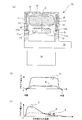
- FIGS. 1 (a) to 1 (c) 1A is a cross-sectional view of a plasma CVD apparatus having an inner cylinder
- FIG. 1B is a graph showing a plasma potential profile along line A and line B in FIG.
- FIG. 1C is a graph showing the profile of the plasma potential along the C line and the potential along the D line in FIG.
- the plasma CVD apparatus 10 is provided in a cylindrical vacuum chamber 11 made of aluminum, a disk-shaped ceiling plate 12 made of ceramics that closes an upper opening of the vacuum chamber 11, and an interior of the vacuum chamber 11, and is made of a semiconductor or the like. And a cylindrical inner cylinder 15 made of aluminum having a surface anodized and placed on a stepped portion 11 a provided on the inner wall of the vacuum chamber 11. In order to maintain the thermal stability of the inner cylinder 15 itself, the inner cylinder 15 is supported by the protrusion 15a in point contact with the step portion 11a.
- a turbo molecular pump 19 is connected to the lower part of the vacuum chamber 11 through a gate valve 18 for pressure control, and the pressure inside the vacuum chamber 11 is changed by the gate valve 18 and the turbo molecular pump 19 etc. Control is possible.
- the plasma CVD apparatus 10 includes a plasma generation mechanism and a gas supply mechanism on the top of the ceiling plate 12 and on the side of the vacuum chamber 11, but these are not shown here.
- the mounting table 13 has a cylindrical shape and the lower part thereof is supported by the side wall of the vacuum chamber 11, but the illustration thereof is also omitted here.
- the profile of the plasma potential in the radial direction of the vacuum chamber 11 is a graph as shown in FIG.
- the line A in FIG. 1A is a straight line in the radial direction of the vacuum chamber 11 in the plasma generation region P at a position close to the plasma generation mechanism (for example, a plasma antenna that receives high-frequency electromagnetic waves).
- the plasma potential along the line has a profile as shown in the graph A of FIG.
- FIG. 1A is a straight line in the radial direction of the vacuum chamber 11 in the plasma generation region P near the substrate 14, and the plasma potential along the line B is the graph in FIG. The profile is as shown in B. Further, the plasma potential in the central axis direction of the vacuum chamber 11, that is, in the C line, has a profile as shown in the graph C of FIG.
- the plasma potential is substantially constant inside the plasma generation region P, and the vacuum chamber 11 is grounded on the inner wall of the vacuum chamber 11. 0.
- the plasma potential once rises with increasing distance from the ceiling plate 12, and gradually decreases after reaching a peak in the plasma generation region P close to the plasma generation mechanism. To go. Therefore, if the substrate 14 is disposed at a position sufficiently away from the ceiling plate 12, that is, in the plasma diffusion region, plasma processing is performed in a low plasma potential ( ⁇ low electron temperature) state, and plasma damage is suppressed. It becomes possible.
- the height (length) of the inner cylinder 15 needs to be increased according to the arrangement position of the substrate 14.
- the aluminum in the inner cylinder 15 is in an electrically floating state from the vacuum chamber 11 and has a potential due to the generation of plasma.
- the potential along the D line in the height direction of the inner cylinder 15 has a profile as shown in the graph D of FIG. 1C, and a reverse region E having a higher potential than the graph C is present at the lower end portion of the inner cylinder 15. Will occur.
- the reversal region E electrons collide with the lower end portion of the inner cylinder 15 to generate abnormal heating, and when there is a protrusion locally, abnormal discharge is generated between the plasma and the vacuum chamber 11. Will occur.
- the inner cylinder 15 needs to keep the entire inner cylinder 15 at a constant temperature so that the attached product does not peel off. However, when abnormal heating as described above occurs, the product attached to that part peels off. However, there is a risk of causing particles. In addition, when an abnormal discharge occurs, the anodized portion on the surface of the inner cylinder 15 may be peeled off, which may cause particles.
- the substrate 14 becomes a negative potential by using these mechanisms.
- positive ions are generated in the plasma generation region, the plasma potential is shifted positively, and the potential difference in the inversion region E becomes larger. Heating and abnormal discharge become more prominent, and particles due to them may become more prominent.
- the inner cylinder 15 can be easily replaced and is inexpensive. Therefore, it is desired to reduce particles caused by the internal potential of the inner cylinder 15 even if the inner cylinder 15 is used.
- the present invention has been made in view of the above problems, and an object thereof is to provide a plasma processing apparatus and method for reducing particles caused by an internal potential of an inner cylinder installed in a vacuum vessel.
- a plasma processing apparatus for solving the above-mentioned problems is In a plasma processing apparatus that has an inner tube made of aluminum whose surface is anodized inside a metal vacuum vessel, arranges a substrate in the plasma diffusion region, and performs plasma processing, A part of the alumite on the surface of the inner cylinder is peeled off and electrically connected to the vacuum vessel.
- a plasma processing apparatus for solving the above-mentioned problems is as follows.
- the inner cylinder is supported on the vacuum container by point contact, and the alumite at the point contact portion of the inner cylinder is peeled off to be electrically connected to the vacuum container.
- a plasma processing apparatus for solving the above-described problem is
- a plurality of protrusions that make point contact with the vacuum vessel are provided at a lower end portion of the inner cylinder, and an alumite at the tip of the protrusion is peeled off to be electrically connected to the vacuum vessel. .
- a plasma processing apparatus for solving the above-mentioned problems is as follows.
- the surface is made of anodized aluminum and has a gas nozzle arranged on the inner wall of the vacuum vessel and penetrating a through hole provided in the inner cylinder
- the through hole of the inner cylinder is provided with a protrusion that makes point contact with the gas nozzle, and peels off the alumite at the tip of the protrusion
- the alumite on the surface of the gas nozzle of the portion in contact with the protruding portion of the inner cylinder and the portion in contact with the vacuum container is peeled off to electrically connect the inner cylinder and the vacuum container.
- a plasma processing method for solving the above problem is as follows.
- An inner cylinder made of aluminum whose surface is anodized is placed inside a metal vacuum container, and a part of the anodized aluminum on the inner cylinder surface is peeled off to electrically connect the inner cylinder and the vacuum container.
- the plasma processing apparatus and method for performing plasma processing by arranging a substrate in the plasma diffusion region a part of the alumite on the inner cylinder surface is peeled off and electrically connected to the vacuum vessel.
- the internal potential of the inner cylinder By setting the internal potential of the inner cylinder to 0, particles caused by the internal potential can be reduced. As a result, the plasma processing performance and reliability in the plasma processing apparatus and method can be improved.
- (A) is sectional drawing of the plasma processing apparatus which has an inner cylinder
- (b) is a graph which shows the profile of the plasma potential in alignment with the A line and B line of (a)
- (c) is ( It is a graph which shows the plasma potential or the profile of an electric potential along the C line of a), and a D line.
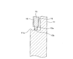
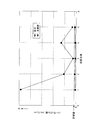
- BRIEF DESCRIPTION OF THE DRAWINGS It is sectional drawing which shows an example (Example 1) of embodiment of the plasma processing apparatus which concerns on this invention, and shows the contact part of an inner cylinder and a vacuum vessel. It is a graph which compares transition of the particle in the conventional plasma processing apparatus, and transition of the particle in the plasma processing apparatus of Example 1.
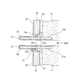
- FIG. The other example (Example 2) of embodiment of the plasma processing apparatus which concerns on this invention is shown, and is sectional drawing which shows the contact part of an inner cylinder and a gas nozzle.
- FIGS. Embodiments of the plasma processing apparatus and method according to the present invention will be described with reference to FIGS.
- this invention presupposes the plasma CVD apparatus shown to Fig.1 (a), the overlapping description is abbreviate
- a plasma CVD apparatus is illustrated as an example, the present invention is not limited to the plasma CVD apparatus but can be applied to a plasma etching apparatus.
- Example 1 In the present embodiment, as shown in FIG. 1A, an inner cylinder 15 made of aluminum whose surface is anodized is disposed inside a metal vacuum chamber (vacuum container) 11. This is based on a plasma CVD apparatus 10 in which a substrate 14 is disposed at a position of a plasma diffusion region and plasma processing is performed on the substrate 14.
- the inner cylinder 15 prevents the product from adhering to the inner wall surface of the vacuum chamber 11 and protects the inner wall surface of the vacuum chamber 11 from being exposed to plasma.
- the inner cylinder 15 has a plurality of (at least three) protrusions 15a at the lower end thereof so as to be supported by the stepped portion 11a of the vacuum chamber 11 by point contact.
- the entire surface of the inner cylinder 15 is formed with an alumite coating 16 by alumite treatment, but the tip 15b of the projection 15a, that is, the alumite coating 16 at the point contact portion is peeled off to electrically connect with the vacuum chamber 11.
- the continuity is maintained.
- the inner wall of the vacuum chamber 11 may also be formed with an alumite coating by anodizing, but in that case, only the stepped portion 11a is peeled off and the electrical connection with the inner cylinder 15 is maintained.
- the inner cylinder 15 needs to keep the entire inner cylinder 15 at a constant temperature so that the attached product does not peel off. Therefore, as described above, the thermal contact with the vacuum chamber 11 is in a point contact state, and in addition, a gap that does not contact the inner wall surface of the vacuum chamber 11, for example, an interval of about 0.5 mm is provided. , Installed inside the vacuum chamber 11. When installed in this way, the temperature is stabilized at a substantially constant temperature by heat input from the plasma and cooling from the vacuum chamber 11.
- FIG. 3 shows a graph comparing the transition of particles after plasma cleaning in a conventional plasma CVD apparatus and the transition of particles after plasma cleaning in the plasma CVD apparatus of this embodiment.
- the entire inner surface of the inner cylinder 15 is alumite-treated and there is no electrical conduction portion.
- the entire inner surface of the inner cylinder 15 is While being alumite-treated, a portion (only the tip portion 15b) is provided with an electrically conducting portion.
- the level of the particles exceeds the allowable value. It is.
- the level is reduced from the first sheet to a particle level that falls below the allowable value.
- Example 2 This embodiment is also based on the plasma CVD apparatus 10 shown in FIG. However, in the first embodiment, the electrically conductive portion is provided at the lower end portion (tip portion 15b) of the inner cylinder 15, but when there is no structure like the step portion 11a, for example, a gas nozzle that penetrates the inner cylinder 15 21 may be provided on the inner wall of the vacuum chamber 11, and the inner cylinder 15 may be electrically connected to the gas nozzle 21.
- a gas nozzle that penetrates the inner cylinder 15 21 may be provided on the inner wall of the vacuum chamber 11, and the inner cylinder 15 may be electrically connected to the gas nozzle 21.
- a plurality of gas nozzles 21 penetrating the inner cylinder 15 from the inner wall of the vacuum chamber 11 are provided.
- the gas nozzle 21 may be installed at any position between the height position of the ceiling plate 12 and the height position of the substrate 14, but a position closer to the ceiling plate 12 is desirable.
- the gas nozzle 21 has a cylindrical shape, and is formed of aluminum having an anodized surface as in the case of the inner cylinder 15. However, in the gas nozzle 21, the alumite coating 22 is peeled off at the contact portion 21 a that contacts the inner cylinder 15 and the contact portion 21 b that contacts the vacuum chamber 11.
- the inner cylinder 15 is provided with a through hole 17 through which the gas nozzle 21 penetrates.
- a plurality of protrusions 15c that are in point contact with the gas nozzle 21 are formed inside the through hole 17, and the tip 15d of the tip 15d is formed.
- the anodized coating 16 is peeled off. Therefore, electrically, the inner cylinder 15 and the vacuum chamber 11 are kept connected via the gas nozzle 21. On the other hand, thermally, the protrusion 15c is in a point contact state with the contact portion 21a.
- the inner cylinder 15 is electrically connected to the vacuum chamber 11 as in the first embodiment, the potential of the aluminum portion inside the inner cylinder 15 becomes 0, as shown in FIG.
- the reversal region E does not occur. Therefore, electric field concentration is not caused, electrons do not collide locally, and abnormal heating and abnormal discharge do not occur. As a result, particles due to the internal potential are reduced.
- the inner cylinder 15 is thermally in a point contact state with the vacuum chamber 11 side, and a gap that does not contact the inner wall surface of the vacuum chamber 11, for example, It is installed inside the vacuum chamber 11 with an interval of about 0.5 mm. By installing in this way, the entire inner cylinder 15 is kept at a constant temperature so that the attached product does not peel off.
- the present invention is suitable for a plasma processing apparatus, such as a plasma CVD apparatus or a plasma etching apparatus, which has an inner cylinder made of aluminum whose surface is anodized and arranges a substrate in a plasma diffusion region to perform plasma processing.
- the plasma processing method is suitable for plasma CVD and plasma etching.
Landscapes
- Chemical & Material Sciences (AREA)
- Engineering & Computer Science (AREA)
- Physics & Mathematics (AREA)
- Plasma & Fusion (AREA)
- Analytical Chemistry (AREA)
- Chemical Kinetics & Catalysis (AREA)
- General Chemical & Material Sciences (AREA)
- Materials Engineering (AREA)
- Mechanical Engineering (AREA)
- Metallurgy (AREA)
- Organic Chemistry (AREA)
- Chemical Vapour Deposition (AREA)
- Plasma Technology (AREA)
- Drying Of Semiconductors (AREA)
Abstract
Description
プラズマCVD装置10は、アルミニウムからなる円筒形状の真空チャンバ11と、真空チャンバ11の上部開口部を閉塞するセラミックスからなる円盤状の天井板12と、真空チャンバ11の内部に設けられ、半導体等からなる基板14を支持する載置台13と、真空チャンバ11の内壁に設けられた段差部11a上に設置され、表面をアルマイト処理したアルミニウムからなる円筒状の内筒15とを有する。この内筒15は、内筒15自体の熱的安定状態を保つため、突起部15aにより、段差部11aとは点接触にて支持されている。
金属製の真空容器の内部に、表面をアルマイト処理したアルミニウムからなる内筒を有し、プラズマ拡散領域に基板を配置して、プラズマ処理を行うプラズマ処理装置において、
前記内筒表面のアルマイトを一部剥離して、前記真空容器と電気的に導通させたことを特徴とする。
上記第1の発明に記載のプラズマ処理装置において、
前記内筒を前記真空容器に点接触で支持させると共に、前記内筒の点接触部分のアルマイトを剥離して、前記真空容器と電気的に導通させたことを特徴とする。
上記第2の発明に記載のプラズマ処理装置において、
前記内筒の下端部に、前記真空容器と点接触する複数の突起部を設けると共に、当該突起部の先端のアルマイトを剥離して、前記真空容器と電気的に導通させたことを特徴とする。
上記第1の発明に記載のプラズマ処理装置において、
表面をアルマイト処理したアルミニウムからなり、前記真空容器の内側壁に設けると共に前記内筒に設けた貫通孔を貫通させて配置したガスノズルを有する場合、
前記内筒の貫通孔に、前記ガスノズルと点接触する突起部を設けると共に、当該突起部の先端のアルマイトを剥離し、
前記内筒の突起部と点接触する部分及び前記真空容器と接触する部分の前記ガスノズル表面のアルマイトを剥離して、前記内筒と前記真空容器とを電気的に導通させたことを特徴とする。
金属製の真空容器の内部に、表面をアルマイト処理したアルミニウムからなる内筒を配置すると共に、当該内筒表面のアルマイトの一部を剥離して、前記内筒と前記真空容器とを電気的に導通させ、
前記真空容器内部のプラズマ拡散領域の位置に基板を配置し、
前記基板に対して、プラズマ処理を行うことを特徴とする。
11 真空チャンバ
12 天井板
13 載置台
14 基板
15 内筒
16 アルマイト
17 貫通孔
21 ガスノズル
本実施例は、図1(a)に示したように、金属製の真空チャンバ(真空容器)11の内部に、表面をアルマイト処理したアルミニウムからなる内筒15を配置し、真空チャンバ11内部のプラズマ拡散領域の位置に基板14を配置し、基板14に対して、プラズマ処理を行うプラズマCVD装置10を前提とするものである。なお、内筒15は、真空チャンバ11の内壁面への生成物の付着を防止すると共に、真空チャンバ11の内壁面をプラズマに曝されることから保護している。
本実施例も、図1(a)に示したプラズマCVD装置10を前提とするものである。しかしながら、実施例1では、内筒15の下端部(先端部15b)に電気的導通箇所を設けたが、段差部11aのような構造が無い場合には、例えば、内筒15を貫通するガスノズル21を真空チャンバ11の内側壁に設け、このガスノズル21に内筒15が電気的に導通するように構成してもよい。このような構成について、図4を参照して、説明する。
Claims (5)
- 金属製の真空容器の内部に、表面をアルマイト処理したアルミニウムからなる内筒を有し、プラズマ拡散領域に基板を配置して、プラズマ処理を行うプラズマ処理装置において、
前記内筒表面のアルマイトを一部剥離して、前記真空容器と電気的に導通させたことを特徴とするプラズマ処理装置。 - 請求項1に記載のプラズマ処理装置において、
前記内筒を前記真空容器に点接触で支持させると共に、前記内筒の点接触部分のアルマイトを剥離して、前記真空容器と電気的に導通させたことを特徴とするプラズマ処理装置。 - 請求項2に記載のプラズマ処理装置において、
前記内筒の下端部に、前記真空容器と点接触する複数の突起部を設けると共に、当該突起部の先端のアルマイトを剥離して、前記真空容器と電気的に導通させたことを特徴とするプラズマ処理装置。 - 請求項1に記載のプラズマ処理装置において、
表面をアルマイト処理したアルミニウムからなり、前記真空容器の内側壁に設けると共に前記内筒に設けた貫通孔を貫通させて配置したガスノズルを有する場合、
前記内筒の貫通孔に、前記ガスノズルと点接触する突起部を設けると共に、当該突起部の先端のアルマイトを剥離し、
前記内筒の突起部と点接触する部分及び前記真空容器と接触する部分の前記ガスノズル表面のアルマイトを剥離して、前記内筒と前記真空容器とを電気的に導通させたことを特徴とするプラズマ処理装置。 - 金属製の真空容器の内部に、表面をアルマイト処理したアルミニウムからなる内筒を配置すると共に、当該内筒表面のアルマイトの一部を剥離して、前記内筒と前記真空容器とを電気的に導通させ、
前記真空容器内部のプラズマ拡散領域の位置に基板を配置し、
前記基板に対して、プラズマ処理を行うことを特徴とするプラズマ処理方法。
Priority Applications (3)
| Application Number | Priority Date | Filing Date | Title |
|---|---|---|---|
| US13/322,192 US8960124B2 (en) | 2009-06-11 | 2010-05-24 | Plasma processing apparatus and plasma processing method |
| KR1020117029464A KR101421331B1 (ko) | 2009-06-11 | 2010-05-24 | 플라즈마 처리 장치 및 플라즈마 처리 방법 |
| EP10786056A EP2441859A1 (en) | 2009-06-11 | 2010-05-24 | Plasma processing apparatus and plasma processing method |
Applications Claiming Priority (2)
| Application Number | Priority Date | Filing Date | Title |
|---|---|---|---|
| JP2009139795A JP5351625B2 (ja) | 2009-06-11 | 2009-06-11 | プラズマ処理装置 |
| JP2009-139795 | 2009-06-11 |
Publications (1)
| Publication Number | Publication Date |
|---|---|
| WO2010143525A1 true WO2010143525A1 (ja) | 2010-12-16 |
Family
ID=43308780
Family Applications (1)
| Application Number | Title | Priority Date | Filing Date |
|---|---|---|---|
| PCT/JP2010/058734 Ceased WO2010143525A1 (ja) | 2009-06-11 | 2010-05-24 | プラズマ処理装置及び方法 |
Country Status (6)
| Country | Link |
|---|---|
| US (1) | US8960124B2 (ja) |
| EP (1) | EP2441859A1 (ja) |
| JP (1) | JP5351625B2 (ja) |
| KR (1) | KR101421331B1 (ja) |
| TW (1) | TWI419616B (ja) |
| WO (1) | WO2010143525A1 (ja) |
Cited By (1)
| Publication number | Priority date | Publication date | Assignee | Title |
|---|---|---|---|---|
| CN105002477A (zh) * | 2015-08-27 | 2015-10-28 | 广东先导稀材股份有限公司 | 一种石墨沉积装置及其制备方法 |
Families Citing this family (3)
| Publication number | Priority date | Publication date | Assignee | Title |
|---|---|---|---|---|
| US10657999B2 (en) | 2014-06-20 | 2020-05-19 | Advanced Material Technologies, Inc. | Plasma CVD device and method of manufacturing magnetic recording medium |
| KR102452084B1 (ko) * | 2015-09-22 | 2022-10-11 | (주) 엔피홀딩스 | 파티클 저감을 위한 플라즈마 반응기 |
| CN114068273B (zh) * | 2020-07-31 | 2024-04-05 | 中微半导体设备(上海)股份有限公司 | 一种零部件及其制备方法和等离子体反应装置 |
Citations (6)
| Publication number | Priority date | Publication date | Assignee | Title |
|---|---|---|---|---|
| JPH02183533A (ja) * | 1989-01-10 | 1990-07-18 | Fujitsu Ltd | プラズマ気相成長装置の汚染防止方法 |
| JPH08172080A (ja) * | 1994-08-15 | 1996-07-02 | Applied Materials Inc | 壁腐食に対する表面保護手段を有するプラズマエッチングリアクタ |
| JPH1038300A (ja) * | 1996-07-25 | 1998-02-13 | Fuji Kogyo Kk | 浴室換気乾燥機 |
| JPH10321559A (ja) * | 1997-05-19 | 1998-12-04 | Hitachi Ltd | 半導体装置の製造方法 |
| JP2000173931A (ja) * | 1998-12-07 | 2000-06-23 | Sony Corp | 処理室のシールド構造及びこれを使用するcvd装置、pvd装置及びエッチング装置 |
| JP2005191023A (ja) | 2003-12-24 | 2005-07-14 | Mitsubishi Heavy Ind Ltd | プラズマ処理装置 |
Family Cites Families (9)
| Publication number | Priority date | Publication date | Assignee | Title |
|---|---|---|---|---|
| US5891350A (en) | 1994-12-15 | 1999-04-06 | Applied Materials, Inc. | Adjusting DC bias voltage in plasma chambers |
| JP3288910B2 (ja) | 1995-12-21 | 2002-06-04 | 株式会社東芝 | 半導体装置の製造方法 |
| US6258170B1 (en) * | 1997-09-11 | 2001-07-10 | Applied Materials, Inc. | Vaporization and deposition apparatus |
| JP4037956B2 (ja) | 1998-04-28 | 2008-01-23 | 東海カーボン株式会社 | チャンバー内壁保護部材 |
| US6170429B1 (en) * | 1998-09-30 | 2001-01-09 | Lam Research Corporation | Chamber liner for semiconductor process chambers |
| US6779481B2 (en) * | 2000-04-27 | 2004-08-24 | Tokyo Electron Limited | Electrical coupling between chamber parts in electronic device processing equipment |
| US7137353B2 (en) * | 2002-09-30 | 2006-11-21 | Tokyo Electron Limited | Method and apparatus for an improved deposition shield in a plasma processing system |
| JP4141234B2 (ja) | 2002-11-13 | 2008-08-27 | キヤノンアネルバ株式会社 | プラズマ処理装置 |
| US20070215278A1 (en) * | 2006-03-06 | 2007-09-20 | Muneo Furuse | Plasma etching apparatus and method for forming inner wall of plasma processing chamber |
-
2009
- 2009-06-11 JP JP2009139795A patent/JP5351625B2/ja not_active Expired - Fee Related
-
2010
- 2010-05-24 EP EP10786056A patent/EP2441859A1/en not_active Withdrawn
- 2010-05-24 KR KR1020117029464A patent/KR101421331B1/ko not_active Expired - Fee Related
- 2010-05-24 US US13/322,192 patent/US8960124B2/en not_active Expired - Fee Related
- 2010-05-24 WO PCT/JP2010/058734 patent/WO2010143525A1/ja not_active Ceased
- 2010-05-27 TW TW099117028A patent/TWI419616B/zh not_active IP Right Cessation
Patent Citations (6)
| Publication number | Priority date | Publication date | Assignee | Title |
|---|---|---|---|---|
| JPH02183533A (ja) * | 1989-01-10 | 1990-07-18 | Fujitsu Ltd | プラズマ気相成長装置の汚染防止方法 |
| JPH08172080A (ja) * | 1994-08-15 | 1996-07-02 | Applied Materials Inc | 壁腐食に対する表面保護手段を有するプラズマエッチングリアクタ |
| JPH1038300A (ja) * | 1996-07-25 | 1998-02-13 | Fuji Kogyo Kk | 浴室換気乾燥機 |
| JPH10321559A (ja) * | 1997-05-19 | 1998-12-04 | Hitachi Ltd | 半導体装置の製造方法 |
| JP2000173931A (ja) * | 1998-12-07 | 2000-06-23 | Sony Corp | 処理室のシールド構造及びこれを使用するcvd装置、pvd装置及びエッチング装置 |
| JP2005191023A (ja) | 2003-12-24 | 2005-07-14 | Mitsubishi Heavy Ind Ltd | プラズマ処理装置 |
Cited By (2)
| Publication number | Priority date | Publication date | Assignee | Title |
|---|---|---|---|---|
| CN105002477A (zh) * | 2015-08-27 | 2015-10-28 | 广东先导稀材股份有限公司 | 一种石墨沉积装置及其制备方法 |
| CN105002477B (zh) * | 2015-08-27 | 2018-06-29 | 广东先导稀材股份有限公司 | 一种石墨沉积装置及其制备方法 |
Also Published As
| Publication number | Publication date |
|---|---|
| US20120125891A1 (en) | 2012-05-24 |
| JP2010285650A (ja) | 2010-12-24 |
| EP2441859A1 (en) | 2012-04-18 |
| KR20120014201A (ko) | 2012-02-16 |
| TW201130389A (en) | 2011-09-01 |
| TWI419616B (zh) | 2013-12-11 |
| JP5351625B2 (ja) | 2013-11-27 |
| US8960124B2 (en) | 2015-02-24 |
| KR101421331B1 (ko) | 2014-07-18 |
Similar Documents
| Publication | Publication Date | Title |
|---|---|---|
| US8651049B2 (en) | Plasma processing apparatus | |
| US9099503B2 (en) | Plasma processing apparatus | |
| KR101176745B1 (ko) | 플라즈마 처리 장치 | |
| KR101317018B1 (ko) | 플라즈마 처리 장치 | |
| JP6063741B2 (ja) | プラズマ処理容器及びプラズマ処理装置 | |
| US20070227666A1 (en) | Plasma processing apparatus | |
| KR20170116195A (ko) | 분리가능한 고 저항률 가스 분배 플레이트를 갖는 샤워헤드 | |
| JPWO1998046808A1 (ja) | 処理装置 | |
| US20070227663A1 (en) | Substrate processing apparatus and side wall component | |
| JP5351625B2 (ja) | プラズマ処理装置 | |
| US20190360102A1 (en) | Isolator for a substrate processing chamber | |
| US20200144090A1 (en) | Placing table and substrate processing apparatus | |
| US20210280449A1 (en) | Stage and plasma processing apparatus | |
| US12027349B2 (en) | Plasma processing apparatus | |
| US11201039B2 (en) | Mounting apparatus for object to be processed and processing apparatus | |
| JP2013241679A (ja) | プラズマ処理装置及び方法 | |
| CN102034678A (zh) | 真空处理装置 | |
| KR20210076973A (ko) | 반응 챔버 라이닝 | |
| TWI839675B (zh) | 下電極組件及等離子體處理裝置 | |
| JP5640135B2 (ja) | プラズマ処理装置 | |
| JP2011124295A (ja) | プラズマ処理装置 | |
| JP5064708B2 (ja) | プラズマ処理装置 | |
| CN114823270A (zh) | 紧固构造、等离子体处理装置以及紧固方法 | |
| US20220068613A1 (en) | Plasma processing equipment | |
| JP2013093480A (ja) | プラズマ処理装置 |
Legal Events
| Date | Code | Title | Description |
|---|---|---|---|
| 121 | Ep: the epo has been informed by wipo that ep was designated in this application |
Ref document number: 10786056 Country of ref document: EP Kind code of ref document: A1 |
|
| WWE | Wipo information: entry into national phase |
Ref document number: 2010786056 Country of ref document: EP |
|
| ENP | Entry into the national phase |
Ref document number: 20117029464 Country of ref document: KR Kind code of ref document: A |
|
| NENP | Non-entry into the national phase |
Ref country code: DE |
|
| WWE | Wipo information: entry into national phase |
Ref document number: 13322192 Country of ref document: US |