WO2010143533A1 - Appareil électronique - Google Patents
Appareil électronique Download PDFInfo
- Publication number
- WO2010143533A1 WO2010143533A1 PCT/JP2010/058817 JP2010058817W WO2010143533A1 WO 2010143533 A1 WO2010143533 A1 WO 2010143533A1 JP 2010058817 W JP2010058817 W JP 2010058817W WO 2010143533 A1 WO2010143533 A1 WO 2010143533A1
- Authority
- WO
- WIPO (PCT)
- Prior art keywords
- power
- mode
- power supply
- request
- state
- Prior art date
- Legal status (The legal status is an assumption and is not a legal conclusion. Google has not performed a legal analysis and makes no representation as to the accuracy of the status listed.)
- Ceased
Links
Images


Classifications
-
- H—ELECTRICITY
- H04—ELECTRIC COMMUNICATION TECHNIQUE
- H04N—PICTORIAL COMMUNICATION, e.g. TELEVISION
- H04N23/00—Cameras or camera modules comprising electronic image sensors; Control thereof
- H04N23/60—Control of cameras or camera modules
- H04N23/65—Control of camera operation in relation to power supply
- H04N23/651—Control of camera operation in relation to power supply for reducing power consumption by affecting camera operations, e.g. sleep mode, hibernation mode or power off of selective parts of the camera
Definitions
- the present invention relates to an electronic device that controls power supply to a device that is not the main device of the device main body when the power supply to the main device of the device main body is stopped in the electronic device.
- the power supply to the circuit system that does not need to operate during the stop is shifted to the shutdown state, If the battery charge is greater than the threshold value, to reduce the startup processing time when restarting, perform the processing required at startup in advance at the time of stop, and shift to the standby state to maintain that state As a result, the system startup time can be shortened and the system can be started up normally.
- the device when the amount of charge of the battery when receiving the stop command is larger than the threshold value, the device is inevitably in a standby state, and the user is scheduled to perform an operation for restarting next. Even when there is no power, power is supplied to the volatile memory, and unnecessary power is supplied to the volatile memory. In view of such a case, a method of shortening the time for supplying power to the volatile memory when receiving a stop command so that unnecessary power is not supplied to the volatile memory can be considered. It is necessary to make the restart command within the time, and if the command cannot be given within the time, the loading process is executed as described above, and the time until the start is started. It will take.
- the present invention solves the above problems, and when an instruction to stop the function of a part of the device main body (main device) is made, the power supply to the device related to the function is stopped, It is an object of the present invention to provide an electronic device that supplies power to a volatile memory for an optimal period.
- the electronic device of the present invention includes the following: a volatile memory in which operation information for operating the device main body is stored; a first power for holding the operation information stored in the volatile memory and the device main body Power supply means for supplying second power to maintain the operating state for the device; a request reception for receiving a non-operating state request for shifting the device main body from the operating state to a non-operating state where a part of the device main body does not operate Means: power supply control means for controlling the power supply means to supply only the first power over a predetermined period when the non-operating state request is accepted by the request accepting means; Mode discriminating means for discriminating the mode; and setting means for setting a predetermined period according to the mode discriminated by the mode discriminating unit.
- the electronic apparatus of the present invention when an instruction to stop the function of a part of the apparatus main body (main device) is given, the supply of power to the device related to the function is stopped and the volatilization is performed for an optimum period. Power can be supplied to the memory.
- FIG. 1 shows a block diagram of the digital camera 10.
- the digital camera 10 includes an optical lens 16 and a diaphragm (not shown), and an optical image of a subject is taken into the CMOS imager unit 18 through an optical lens 16 and a diaphragm controlled by a motor driving unit (not shown) according to an instruction from the main CPU 22. Then, a digital image pickup signal for one frame is output from the CMOS imager unit 18 by a capture pulse given by a timing generator (not shown) connected to the main CPU 22.
- the CMOS imager unit 18 amplifies the charge accumulated in each pixel, reads out the signal from each pixel as a signal, and performs gain adjustment, clamp processing, and A / D conversion processing on the signal. Apply.
- the digital image pickup signal subjected to the processing has one of R, G, and B color signals for each pixel, and is temporarily stored in the SDRAM 32 via the bus 40 under the control of the main CPU 22.
- the digital imaging signal once stored in the SDRAM 32 is input to the signal processing circuit 20 under the control of the main CPU 22.
- the signal processing circuit 20 performs color separation processing on the input digital imaging signal, and further converts it into Y, U, and V signals by YUV conversion. Then, the digital image signal converted by the signal processing circuit 20 is stored in the SDRAM 32 again via the bus 40.
- a process from when the digital image signal output from the CMOS imager unit 18 described above is converted into a digital image signal by the signal processing circuit 20 and stored in the SDRAM 32 is defined as an imaging process.
- the digital image signal stored in the SDRAM 32 is output to the LCD 38 under the control of the main CPU 22.
- the LCD 38 includes an LCD driver (not shown).
- the LCD driver converts Y, U, and V signals into RGB signals, and causes the LCD 38 to display an image signal based on the digital image signal.
- the digital image signal stored in the SDRAM 32 is compressed by a compression / decompression processing unit (not shown) and is stored in an internal memory (not shown) as a JPEG still image file if a still image is to be recorded.
- compression processing is performed by a compression / decompression processing unit (not shown) and stored as an MPEG format moving image file in an internal memory (not shown).
- the operation unit 36 includes a main switch that switches on / off the power supply from the power supply to the digital camera 10 main body (changes from the on state to the off state or from the off state to the on state).
- the power source supplied to a part or the whole of the digital camera 10 is the battery 30 or the external power source 42.
- the external power source 42 is an AC device such as an AC adapter.
- the power control unit 28 supplies power from the external power source 42 to the digital camera 10 instead of power from the battery 30. Control to do.
- the operation unit 36 is connected to the sub CPU 34.
- each operation signal including a signal corresponding to the power on / off operation of the main switch is input to the sub CPU 34.
- the sub CPU 34 is connected to the main CPU 22 and the power control unit 28, and when the operation signal is input, refers to the operation signal and transmits each operation command to the main CPU 22 and the power control unit 28.
- the firmware is software, that is, a program necessary for starting (system starting processing) of the digital camera 20 including the above-described photographing processing.
- the firmware is stored in the nonvolatile memory 26, and when the main CPU 22 transitions from the power supply suspension state to the main power supply state in response to the power-on operation of the main switch, the main CPU 22 stores the firmware in the volatile memory 24. To expand.
- a state in which power from the power source is supplied only to the sub CPU 34 and the power control unit 28 and no power is supplied to other devices is defined as a power supply suspension state
- the power control unit 28 a state in which power from the power source is supplied only to the sub CPU 34 and the volatile memory 24 is defined as a memory power supply state
- a state in which power from the power source is supplied to the entire digital camera 10 is a main power supply state. It is defined as
- the main CPU 22 shifts from the main power supply state to the power supply suspension state via the memory power supply state. Further, even when it is determined by the management of the timer 22a of the main CPU 22 that the operation unit 36 has not been operated by the user for a predetermined time, the power is supplied from the main power supply state via the memory power supply state. Transition to the hibernation state (hereinafter referred to as sleep operation). This power-off operation and sleep operation are operations and operations aimed at power-off.
- a memory such as Expression 1 is used based on coefficients ⁇ , ⁇ , and ⁇ corresponding to a power-off operation or a sleep operation that triggers the transition and other elements that will be described later.
- the state holding time T1 is measured by the timer 28a in the power supply control unit 28, and the time is up when the state holding time T1 has elapsed.
- the power control unit 28 controls the power to shift from the memory power supply state to the power supply suspension state.
- the coefficient ⁇ is a numerical value corresponding to the transition trigger as described above.
- the coefficient ⁇ is stored in an operation lookup table (not shown) in the non-volatile memory 26.
- the coefficient corresponding to the power-off operation is calculated as an operation lookup.
- the table is referenced and stored in the register 22e.
- the operation lookup table values corresponding to the power-off operation and the sleep operation are arranged.
- the main CPU 22 determines that the sleep operation is performed as a trigger for the transition, the coefficient corresponding to the sleep operation is stored in the register 22e with reference to the operation lookup table.
- the coefficient ⁇ corresponding to the power-off operation is smaller than the coefficient ⁇ corresponding to the sleep operation.
- the reason for this is that the power off caused by the power off operation is intended by the user to turn off the power, and the probability of using the digital camera 10 after the power off is short.
- the power off due to the sleep operation is a power off that is not intended by the user, and it is highly likely that the digital camera 10 is used by performing a power on operation by operating the main switch immediately after the power is turned off. It is.
- the state holding time T1 is lengthened, so that when the main switch is turned on within the state holding time T1, the volatile memory 24 is immediately stored. Since the stored firmware can be executed, the activation time of the digital camera 10 can be shortened.
- the coefficient ⁇ is a numerical value corresponding to the voltage level of the battery 30 when the battery 30 is used as a power source.
- the coefficient ⁇ is stored in a voltage lookup table (not shown) in the nonvolatile memory 26. In the voltage lookup table, values corresponding to the voltage levels are arranged.
- the main CPU 22 detects the voltage level of the battery 30, the main CPU 22 refers to the voltage lookup table and stores a coefficient corresponding to the voltage level in the register 22f.
- the coefficient ⁇ when the voltage level is high is larger than the coefficient ⁇ when the voltage level is low.
- the digital camera 10 is immediately executed by executing the firmware stored in the volatile memory 24 when the main switch is turned on within the state holding time T1. This is because the start-up time can be shortened. Further, when the voltage level is low, the life of the battery 30 can be extended by shortening the state holding time T1 to save power.
- the main CPU 22 sets the state storage time T1 infinitely without detecting the coefficients ⁇ and ⁇ because the power supply is not interrupted.
- the coefficient ⁇ is a numerical value corresponding to the current time set in the digital camera 10.
- the coefficient ⁇ is stored in a time lookup table (not shown) in the nonvolatile memory 26. In the time lookup table, values corresponding to times are arranged.
- the main CPU 22 refers to the time look-up table and stores a coefficient corresponding to the detected time in the register 22g.
- the coefficient ⁇ of the midnight time is smaller than the coefficient ⁇ of the time when the user's activity is relatively high, not at midnight.
- the reason is that the user may use the digital camera 10 at a time when the user's activity is relatively high rather than at midnight, rather than when the time is detected at midnight. Therefore, if the main switch is turned on within the state holding time T1, the firmware stored in the volatile memory 24 is immediately executed by increasing the state holding time T1. Thus, the startup time of the digital camera 10 can be shortened. When the time is detected at midnight, the life of the battery 30 can be extended by shortening the state holding time T1 to save power.
- the control for switching from the main power supply state to the power supply suspension state via the memory power supply state by performing the power-off operation or the sleep operation described above is performed by the main CPU 22, the sub CPU 34, and the power control unit 28.
- This is realized by executing each program developed from the nonvolatile memory 26 to the volatile memory 24 by a microcomputer (not shown).
- the digital camera 10 has a multitasking environment, and the main CPU 22 can execute a plurality of tasks simultaneously.
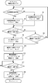
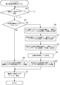
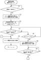
- the power management task, sleep transition task, power supply time calculation task, and power control task that are executed by the sub CPU 34, the main CPU 22, and the microcomputer (not shown) of the power controller 28 will be described below with reference to FIGS. I will explain.
- FIG. 2 shows a flowchart of the power management task executed by the sub CPU 34.
- step S15 a command corresponding to the power-off instruction to the main device is sent to the power control unit 28, and the process proceeds to step S17.
- step S ⁇ b> 17 it is determined whether or not the user has performed a power-on operation by operating the main switch, and the determination is repeatedly performed until it is determined YES. If YES is determined in the step S17, the process proceeds to a step S19 so as to send a command corresponding to a power-on instruction to the main device to the power control unit 28, and the process returns to the step S1.
- step S57 the voltage level of the battery 30 is detected, and the coefficient ⁇ corresponding to the voltage level is stored in the register 22f with reference to the voltage lookup table.
- step S59 the current time is detected from the clock 22d, and the coefficient ⁇ corresponding to the detected time is stored in the register 22g by referring to the time lookup table.
- step S61 the state holding time T1 is calculated, and the process proceeds to step S63.
- step S63 a request command is transmitted to set the state holding time T1 calculated in step S61 in the register 28b of the power supply control unit 28, and the process proceeds to step S67.
- step S53 If YES is determined in step S53, the process proceeds to step S65, a request command is transmitted to the power supply control unit 28 in order to set the state holding time T1 to infinity in the register 28b, and the process proceeds to step S67.
- step S71 it is determined whether or not there is a command corresponding to a power-off instruction from the sub CPU 34 to the main device. The determination is repeated until YES is determined in step S71, and if YES is determined, the process proceeds to step S73, the power of the battery 30 or the external power source 42 is controlled, and the transition from the main power supply state to the memory power supply state is made.
- step S75 the state holding time T1 stored in the register 28b is set in the timer 28a, and measurement is started.
- the process proceeds to step S77, where it is determined whether or not there is a power-on request from the sub CPU 34 to the main device. If YES is determined in the step S77, the process proceeds to a step S79 so as to control the power of the battery 30 or the external power source 42 to shift from the current power supply suspension state to the main power supply state. Then, the process returns to step S71.
- step S77 If it is determined as NO in step S77, the process proceeds to step S81, where it is determined whether or not the timer 28a has timed up, and if it is determined as NO, the process returns to step S77. If YES is determined in the step S81, the process proceeds to a step S83 so as to control the electric power of the battery 30 or the external power source 42 to shift from the memory power supply state to the power supply suspension state. Then, the process proceeds to step S85, and it is determined whether or not there is a power-on request from the sub CPU 28 to the main device. The determination is repeated until it is determined as YES, and when it is determined as YES, the process proceeds to step S79.
- the firmware executed by the main CPU 22 when the next digital camera 10 is activated is nonvolatile.
- the period during which the power is supplied from the volatile memory 24 and stored in the volatile memory 24 so that the firmware is not volatilized is varied according to the trigger mode. Therefore, it is possible to optimize the balance between increasing the startup time of the digital camera 10 and suppressing unnecessary power supply in accordance with the user's application.
- the control for switching from the main power supply state to the power supply suspension state via the memory power supply state by performing the power-off operation or the sleep operation is performed by the main CPU 22, the sub CPU 34, and This is realized by executing a program developed from the nonvolatile memory 26 to the volatile memory 24 by a microcomputer (not shown) of the power supply control unit 28, but the control may be processed by one CPU. Further, other CPUs or microcomputers may be prepared for distributed processing.
- the present invention is applied to the digital camera 10.
- the present invention is not limited to the digital camera 10, and may be applied to an IC recorder, a digital photo frame, a music reproduction music device, a television, and the like.
- the lens 16, the CMOS imager unit 18, the signal processing circuit 20, the LCD 38, and the like of this embodiment are replaced with functions of respective devices.
- the CMOS imager unit 18 is applied as the image pickup device, but a CCD imager may be applied instead of the CMOS imager.
- the power management task, the sleep transition task, the power supply time calculation task, and the power control task have been described by applying software processing so that they are executed by the sub CPU 34, the main CPU 22, and the power control unit 28. , Some or all may be applied to be executed by hard processing.
- the image signal based on the digital image signal is displayed on the LCD 38, but the organic EL may be applied to display the image signal.
Landscapes
- Engineering & Computer Science (AREA)
- Multimedia (AREA)
- Signal Processing (AREA)
- Studio Devices (AREA)
- Power Sources (AREA)
Abstract
Priority Applications (2)
| Application Number | Priority Date | Filing Date | Title |
|---|---|---|---|
| US13/376,627 US20120079300A1 (en) | 2009-06-09 | 2010-05-25 | Electronic apparatus |
| CN2010800253611A CN102461154A (zh) | 2009-06-09 | 2010-05-25 | 电子设备 |
Applications Claiming Priority (2)
| Application Number | Priority Date | Filing Date | Title |
|---|---|---|---|
| JP2009138290A JP2010287950A (ja) | 2009-06-09 | 2009-06-09 | 電子機器 |
| JP2009-138290 | 2009-06-09 |
Publications (1)
| Publication Number | Publication Date |
|---|---|
| WO2010143533A1 true WO2010143533A1 (fr) | 2010-12-16 |
Family
ID=43308788
Family Applications (1)
| Application Number | Title | Priority Date | Filing Date |
|---|---|---|---|
| PCT/JP2010/058817 Ceased WO2010143533A1 (fr) | 2009-06-09 | 2010-05-25 | Appareil électronique |
Country Status (4)
| Country | Link |
|---|---|
| US (1) | US20120079300A1 (fr) |
| JP (1) | JP2010287950A (fr) |
| CN (1) | CN102461154A (fr) |
| WO (1) | WO2010143533A1 (fr) |
Families Citing this family (7)
| Publication number | Priority date | Publication date | Assignee | Title |
|---|---|---|---|---|
| JP2012163923A (ja) * | 2011-02-09 | 2012-08-30 | Ricoh Co Ltd | 測距装置と方法とプログラム並びに撮像装置と方法とプログラム |
| JP5340335B2 (ja) * | 2011-03-24 | 2013-11-13 | 株式会社東芝 | 情報処理装置 |
| KR102296696B1 (ko) | 2012-01-23 | 2021-09-02 | 가부시키가이샤 한도오따이 에네루기 켄큐쇼 | 반도체 장치 |
| US9444509B2 (en) | 2012-09-27 | 2016-09-13 | Intel Corporation | Non-blocking power management for on-package input/output architectures |
| US9674590B2 (en) * | 2012-11-28 | 2017-06-06 | Samsung Electronics Co., Ltd. | System and method for managing sensor information in portable terminal |
| JP6123514B2 (ja) * | 2013-06-25 | 2017-05-10 | ソニー株式会社 | 電子機器、電子機器の制御方法およびプログラム |
| JP7374622B2 (ja) * | 2019-06-17 | 2023-11-07 | キヤノン株式会社 | 情報処理装置 |
Citations (3)
| Publication number | Priority date | Publication date | Assignee | Title |
|---|---|---|---|---|
| JP2001069397A (ja) * | 1999-08-26 | 2001-03-16 | Canon Inc | 撮像装置及びその制御方法 |
| JP2005070681A (ja) * | 2003-08-27 | 2005-03-17 | Casio Electronics Co Ltd | 印刷装置 |
| JP2005110157A (ja) * | 2003-10-02 | 2005-04-21 | Mitsubishi Electric Corp | カメラ付き携帯電話機および電源制御方法 |
Family Cites Families (2)
| Publication number | Priority date | Publication date | Assignee | Title |
|---|---|---|---|---|
| JP2008167307A (ja) * | 2006-12-28 | 2008-07-17 | Olympus Imaging Corp | デジタルカメラ |
| JP4855953B2 (ja) * | 2007-01-17 | 2012-01-18 | オリンパスイメージング株式会社 | デジタルカメラ |
-
2009
- 2009-06-09 JP JP2009138290A patent/JP2010287950A/ja not_active Ceased
-
2010
- 2010-05-25 CN CN2010800253611A patent/CN102461154A/zh active Pending
- 2010-05-25 WO PCT/JP2010/058817 patent/WO2010143533A1/fr not_active Ceased
- 2010-05-25 US US13/376,627 patent/US20120079300A1/en not_active Abandoned
Patent Citations (3)
| Publication number | Priority date | Publication date | Assignee | Title |
|---|---|---|---|---|
| JP2001069397A (ja) * | 1999-08-26 | 2001-03-16 | Canon Inc | 撮像装置及びその制御方法 |
| JP2005070681A (ja) * | 2003-08-27 | 2005-03-17 | Casio Electronics Co Ltd | 印刷装置 |
| JP2005110157A (ja) * | 2003-10-02 | 2005-04-21 | Mitsubishi Electric Corp | カメラ付き携帯電話機および電源制御方法 |
Also Published As
| Publication number | Publication date |
|---|---|
| JP2010287950A (ja) | 2010-12-24 |
| US20120079300A1 (en) | 2012-03-29 |
| CN102461154A (zh) | 2012-05-16 |
Similar Documents
| Publication | Publication Date | Title |
|---|---|---|
| JP3564031B2 (ja) | 電子スチルカメラ | |
| JP5119136B2 (ja) | 電子装置及びその制御方法 | |
| WO2010143533A1 (fr) | Appareil électronique | |
| US20030142228A1 (en) | Apparatus and method for power saving and rapid response in a digital imaging device | |
| JP5857416B2 (ja) | 撮影装置 | |
| CN1972384B (zh) | 信息处理设备、成像设备、信息处理方法 | |
| CN101873421B (zh) | 成像装置、成像控制方法以及成像控制程序 | |
| US20070159549A1 (en) | Image pickup apparatus and method for controlling the same | |
| JP2006072353A (ja) | ストロボ制御器を備えたディジタルカメラ | |
| JP2006311771A (ja) | 電圧変化検出装置 | |
| JP2009053244A (ja) | モード切替システムおよびカメラ | |
| JP2016208648A (ja) | 電子機器、制御方法およびプログラム | |
| KR102214823B1 (ko) | 촬상 장치 및 그 제어 방법 | |
| JP4328697B2 (ja) | 撮像装置及びその制御方法 | |
| CN118042272A (zh) | 摄像装置、摄像装置的控制方法和计算机可读介质 | |
| JP5293255B2 (ja) | 情報記録再生装置およびデジタルカメラ | |
| JP2004120204A (ja) | デジタルカメラ | |
| JP4261815B2 (ja) | 撮像装置 | |
| JP5125546B2 (ja) | カメラ | |
| JP4508721B2 (ja) | 携帯機器及びその制御方法 | |
| JP2002247420A (ja) | 電子カメラ | |
| US20070147823A1 (en) | Method for controlling the picture capturing process of a digital camera | |
| JP2007036676A (ja) | 撮像装置及び撮像装置の制御方法 | |
| JP2006325148A (ja) | 撮像装置及び撮像方法 | |
| JP2010117782A (ja) | 電子機器 |
Legal Events
| Date | Code | Title | Description |
|---|---|---|---|
| WWE | Wipo information: entry into national phase |
Ref document number: 201080025361.1 Country of ref document: CN |
|
| 121 | Ep: the epo has been informed by wipo that ep was designated in this application |
Ref document number: 10786064 Country of ref document: EP Kind code of ref document: A1 |
|
| WWE | Wipo information: entry into national phase |
Ref document number: 13376627 Country of ref document: US |
|
| NENP | Non-entry into the national phase |
Ref country code: DE |
|
| 122 | Ep: pct application non-entry in european phase |
Ref document number: 10786064 Country of ref document: EP Kind code of ref document: A1 |