WO2010143718A1 - Capteur de courant à équilibre magnétique - Google Patents
Capteur de courant à équilibre magnétique Download PDFInfo
- Publication number
- WO2010143718A1 WO2010143718A1 PCT/JP2010/059959 JP2010059959W WO2010143718A1 WO 2010143718 A1 WO2010143718 A1 WO 2010143718A1 JP 2010059959 W JP2010059959 W JP 2010059959W WO 2010143718 A1 WO2010143718 A1 WO 2010143718A1
- Authority
- WO
- WIPO (PCT)
- Prior art keywords
- magnetic
- magnetic field
- current sensor
- shield
- current
- Prior art date
- Legal status (The legal status is an assumption and is not a legal conclusion. Google has not performed a legal analysis and makes no representation as to the accuracy of the status listed.)
- Ceased
Links
Images




Classifications
-
- B—PERFORMING OPERATIONS; TRANSPORTING
- B82—NANOTECHNOLOGY
- B82Y—SPECIFIC USES OR APPLICATIONS OF NANOSTRUCTURES; MEASUREMENT OR ANALYSIS OF NANOSTRUCTURES; MANUFACTURE OR TREATMENT OF NANOSTRUCTURES
- B82Y25/00—Nanomagnetism, e.g. magnetoimpedance, anisotropic magnetoresistance, giant magnetoresistance or tunneling magnetoresistance
-
- G—PHYSICS
- G01—MEASURING; TESTING
- G01R—MEASURING ELECTRIC VARIABLES; MEASURING MAGNETIC VARIABLES
- G01R33/00—Arrangements or instruments for measuring magnetic variables
- G01R33/02—Measuring direction or magnitude of magnetic fields or magnetic flux
- G01R33/06—Measuring direction or magnitude of magnetic fields or magnetic flux using galvano-magnetic devices
- G01R33/09—Magnetoresistive devices
- G01R33/093—Magnetoresistive devices using multilayer structures, e.g. giant magnetoresistance sensors
-
- G—PHYSICS
- G01—MEASURING; TESTING
- G01R—MEASURING ELECTRIC VARIABLES; MEASURING MAGNETIC VARIABLES
- G01R15/00—Details of measuring arrangements of the types provided for in groups G01R17/00 - G01R29/00, G01R33/00 - G01R33/26 or G01R35/00
- G01R15/14—Adaptations providing voltage or current isolation, e.g. for high-voltage or high-current networks
- G01R15/20—Adaptations providing voltage or current isolation, e.g. for high-voltage or high-current networks using galvano-magnetic devices, e.g. Hall-effect devices, i.e. measuring a magnetic field via the interaction between a current and a magnetic field, e.g. magneto resistive or Hall effect devices
- G01R15/205—Adaptations providing voltage or current isolation, e.g. for high-voltage or high-current networks using galvano-magnetic devices, e.g. Hall-effect devices, i.e. measuring a magnetic field via the interaction between a current and a magnetic field, e.g. magneto resistive or Hall effect devices using magneto-resistance devices, e.g. field plates
-
- G—PHYSICS
- G01—MEASURING; TESTING
- G01R—MEASURING ELECTRIC VARIABLES; MEASURING MAGNETIC VARIABLES
- G01R31/00—Arrangements for testing electric properties; Arrangements for locating electric faults; Arrangements for electrical testing characterised by what is being tested not provided for elsewhere
- G01R31/005—Testing of electric installations on transport means
- G01R31/006—Testing of electric installations on transport means on road vehicles, e.g. automobiles or trucks
Definitions
- the present invention relates to a magnetic balance type current sensor using a magnetoresistive effect element (TMR element, GMR element).
- TMR element magnetoresistive effect element
- a motor In an electric vehicle, a motor is driven using electricity generated by an engine, and the magnitude of the current for driving the motor is detected by, for example, a current sensor.
- a current sensor As this current sensor, a magnetic core having a notch (core gap) in part is arranged around a conductor, and a magnetic detection element is arranged in the core gap.
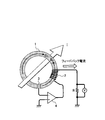
- a current sensor for example, there is a magnetic balance type current sensor as shown in FIG. 23 (Patent Document 1).
- the magnetic balance type current sensor shown in FIG. 23 has a feedback coil 2 wound around the magnetic core 1 in a direction to cancel the magnetic field B1 generated by the current I to be measured.
- the magnetic balance type current sensor when the current I to be measured flows, an output voltage is generated in the magnetic detection element 3 by the magnetic field B1 corresponding to the current, and the voltage signal output from the magnetic detection element 3 is converted into a current.
- Feedback is provided to the feedback coil 2.
- the magnetic field (cancel magnetic field) B2 generated by the feedback coil 2 and the magnetic field B1 generated by the current I to be measured cancel each other so that the magnetic field is always zero. At this time, the feedback current flowing in the feedback coil is converted into a voltage and taken out as an output.
- reference numeral 4 indicates an amplifier
- R indicates a detection resistor.
- Patent Document 2 a magnetic balance type current sensor using a magnetoresistive element without using a magnetic core.
- the present invention has been made in view of the above points, and an object of the present invention is to provide a magnetic balance type current sensor that can save power and reduce the influence of an external magnetic field.
- the magnetic balance type current sensor of the present invention includes a magnetoresistive effect element whose resistance value is changed by application of an induced magnetic field from a current to be measured, and a cancel magnetic field that is disposed in the vicinity of the magnetoresistive effect element and cancels the induced magnetic field.
- a magnetic field detection bridge circuit having two outputs that generate a voltage difference according to the induced magnetic field, a magnetic shield that attenuates the induced magnetic field and enhances the canceling magnetic field, and
- a magnetic balance type current sensor that measures the current to be measured based on a current flowing through the feedback coil when the feedback coil is energized by a voltage difference to achieve an equilibrium state in which the induction magnetic field and the cancellation magnetic field cancel each other.
- the feedback coil, the magnetic shield and the magnetic field detection bridge circuit There characterized by comprising formed on the same substrate.
- This configuration has a magnetic shield adjacent to the feedback coil.
- the magnetic shield can attenuate the induction magnetic field generated from the current to be measured and applied to the magnetoresistive effect element, and can enhance the canceling magnetic field from the feedback coil. Therefore, since the magnetic shield functions as a magnetic yoke, the current flowing through the feedback coil can be reduced, and power saving can be achieved. Moreover, the influence of an external magnetic field can be reduced by this magnetic shield.
- the feedback coil is disposed between the magnetic shield and the magnetic field detection bridge circuit, and the magnetic shield is disposed on a side closer to the current to be measured.
- the magnetoresistive element is preferably a spin valve type GMR element or a TMR element.
- the GMR element has a meander shape with a width of 1 ⁇ m to 10 ⁇ m, a length in the longitudinal direction is at least twice the width, and the longitudinal direction is the inductive magnetic field. It is preferable that they are arranged so as to be both perpendicular to the direction and the direction of the cancellation magnetic field.
- the TMR element is a rectangle having a width of 1 ⁇ m to 10 ⁇ m, the length in the longitudinal direction is at least twice the width, and the longitudinal direction is the direction of the dielectric magnetic field and It is preferable that they are arranged so as to be both perpendicular to the direction of the canceling magnetic field.
- the feedback coil is constituted by a planar coil, and the planar magnetic field is generated so that both the induction magnetic field and the canceling magnetic field are generated in a plane parallel to the plane of formation of the planar coil.
- a coil is preferably provided.
- the magnetic shield is preferably made of a high permeability material selected from the group consisting of an amorphous magnetic material, a permalloy magnetic material, and an iron microcrystalline material. .
- a distance between the magnetoresistive element and the magnetic shield is 2 ⁇ m to 20 ⁇ m.
- the thickness of the magnetic shield is 2 ⁇ m to 20 ⁇ m.
- the dimension of the magnetic shield is 400 ⁇ m to 1000 ⁇ m.
- the magnetic balance type current sensor of the present invention includes a magnetoresistive effect element whose resistance value is changed by application of an induced magnetic field from a current to be measured, and a cancel magnetic field that is disposed in the vicinity of the magnetoresistive effect element and cancels the induced magnetic field.
- a magnetic field detection bridge circuit having two outputs that generate a voltage difference according to the induced magnetic field, a magnetic shield that attenuates the induced magnetic field and enhances the canceling magnetic field, and
- a magnetic balance type current sensor that measures the current to be measured based on a current flowing through the feedback coil when the feedback coil is energized by a voltage difference to achieve an equilibrium state in which the induction magnetic field and the cancellation magnetic field cancel each other.
- the feedback coil, the magnetic shield and the magnetic field detection bridge circuit Since but becomes are formed on the same substrate, it is possible to reduce power consumption, yet it is possible to reduce the influence of an external magnetic field.
- FIG. 1 is a figure which shows the magnetic balance type current sensor which concerns on Embodiment 1 of this invention. It is a figure which shows the magnetic balance type current sensor which concerns on Embodiment 1 of this invention. It is sectional drawing which shows the magnetic balance type current sensor shown in FIG.
- A) is a figure which shows the relationship between GMR-magnetic shield distance and a sensitivity ratio
- (b) is a figure which shows the relationship between GMR-magnetic shield distance and a shield effect.
- (A), (b) is a figure which shows the relationship between a magnetic shield film thickness and an anisotropic magnetic field. It is a figure which shows the relationship between a magnetic shield film thickness and a sensitivity ratio.
- FIG. 1 It is a figure which shows the relationship between an external magnetic field and a secondary current. It is a figure for demonstrating the dimension between a magnetic shield, a feedback coil, and a magnetoresistive effect element.
- (A) is a figure which shows the relationship between a magnetic shield shape and an anisotropic magnetic field.
- A) is a figure which shows the relationship between a magnetic shield shape and a sensitivity
- (b) is a figure which shows the relationship between a magnetic shield shape and a sensitivity ratio.
- (A) is a figure which shows the relationship between the conductor for investigating the relationship between a to-be-measured electric current and an induction magnetic field, and a magnetoresistive effect element
- (b) is between a to-be-measured electric current and an induction magnetic field. It is a figure which shows a relationship.
- (A) is a figure which shows the relationship between the feedback coil and magnetoresistive effect element for investigating the relationship between a feedback current and a cancellation magnetic field
- (b) is the relationship between a feedback current and a cancellation magnetic field.
- FIG. 6 is a circuit diagram showing a magnetic balance type current sensor with an initialization function according to a second embodiment.
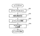
- FIG. FIG. 12 is a flowchart for explaining initialization processing in the second embodiment.
- FIG. 6 is a diagram illustrating a part of a magnetic balanced current sensor according to a third embodiment.
- FIG. 6 is a circuit diagram showing a magnetic balance type current sensor according to a third embodiment.
- FIG. 5 is a diagram showing a magnetic balance type current sensor according to a third embodiment.
- FIG. 11 is a flowchart for illustrating a self test in the third embodiment.
- FIG. 10 is a flowchart for explaining current measurement in the third embodiment. It is a figure which shows the conventional magnetic balance type current sensor.
- FIGS. 1 and 2 are diagrams showing a magnetically balanced current sensor according to Embodiment 1 of the present invention.
- the magnetic balance type current sensor shown in FIGS. 1 and 2 is disposed in the vicinity of the conductor 11 through which the measured current I flows.
- This magnetic balance type current sensor includes a feedback circuit 12 that generates a magnetic field (cancellation magnetic field) that cancels the induced magnetic field caused by the current I to be measured flowing through the conductor 11.
- the feedback circuit 12 includes a feedback coil 121 wound in a direction that cancels the magnetic field generated by the current I to be measured, two magnetoresistive effect elements 122a and 122b that are magnetic detection elements, and two fixed resistance elements 123a, 123b.
- the feedback coil 121 is a planar coil.
- the feedback coil since there is no magnetic core, the feedback coil can be manufactured at low cost. Further, as compared with the case of the toroidal coil, it is possible to prevent the canceling magnetic field generated from the feedback coil from spreading over a wide range and to avoid affecting the peripheral circuits. Furthermore, compared to the toroidal coil, when the current to be measured is an alternating current, the cancellation magnetic field can be easily controlled by the feedback coil, and the current flowing for the control is not so large. About these effects, it becomes so large that a to-be-measured electric current becomes a high frequency by alternating current.
- the planar coil is preferably provided so that both an induction magnetic field and a cancellation magnetic field are generated in a plane parallel to the plane of the planar coil.
- the resistance value of the magnetoresistive effect element 122 changes when an induction magnetic field is applied from the current I to be measured.
- the two magnetoresistive effect elements 122a and 122b constitute a magnetic field detection bridge circuit together with the two fixed resistance elements 123a and 123b.
- This magnetic field detection bridge circuit has two outputs that generate a voltage difference corresponding to the induced magnetic field generated by the current I to be measured.
- a power source Vdd is connected to a connection point between the magnetoresistive effect element 122b and the fixed resistance element 123a, and the magnetoresistive effect element 122a and the fixed resistance element 123b are connected.
- a ground (GND) is connected to the connection point.
- one output is taken out from the connection point between the magnetoresistive effect element 122a and the fixed resistance element 123a, and from the connection point between the magnetoresistive effect element 122b and the fixed resistance element 123b. Another output is taken out.
- This two outputs are amplified by the amplifier 124 and supplied to the feedback coil 121 as a current (feedback current).
- This feedback current corresponds to a voltage difference according to the induced magnetic field.
- a cancellation magnetic field that cancels the induction magnetic field is generated in the feedback coil 121.
- the current to be measured is measured by the detection unit (detection resistor R) based on the current flowing through the feedback coil 121 when the induced magnetic field and the canceling magnetic field cancel each other.
- FIG. 3 is a sectional view showing the magnetic balance type current sensor shown in FIG.
- a feedback coil, a magnetic shield, and a magnetic field detection bridge circuit are formed on the same substrate 21.
- the feedback coil is arranged between the magnetic shield and the magnetic field detection bridge circuit, and the magnetic shield is arranged on the side close to the current I to be measured. That is, the magnetic shield, the feedback coil, and the magnetoresistive element are arranged in this order from the side close to the conductor 11.
- the magnetoresistive effect element can be furthest away from the conductor 11, and the induction magnetic field applied to the magnetoresistive effect element from the current I to be measured can be reduced.
- the magnetic shield can be brought closest to the conductor 11, the attenuation effect of the induced magnetic field can be further enhanced. Therefore, the cancellation magnetic field from the feedback coil can be reduced.
- a thermal silicon oxide film 22 that is an insulating layer is formed on a substrate 21.
- An aluminum oxide film 23 is formed on the thermal silicon oxide film 22.
- the aluminum oxide film 23 can be formed by a method such as sputtering. Further, a silicon substrate or the like is used as the substrate 21.
- magnetoresistive effect elements 122a and 122b are formed on the aluminum oxide film 23, magnetoresistive effect elements 122a and 122b are formed. At this time, fixed resistance elements 123a and 123b are also provided together with the magnetoresistance effect elements 122a and 122b, and a magnetic field detection bridge circuit is built.
- the magnetoresistive elements 122a and 122b TMR elements (tunnel magnetoresistive elements), GMR elements (giant magnetoresistive elements), and the like can be used.
- GMR element a spin valve type GMR element or a spin valve type TMR element constituted by a multilayer film having an antiferromagnetic layer, a fixed magnetic layer, a nonmagnetic layer, and a free magnetic layer can be used.
- the spin valve GMR element is preferably a GMR element having a meander shape as shown in the enlarged view of FIG.
- the width D in the pin direction is preferably 1 ⁇ m to 10 ⁇ m.
- the longitudinal direction is both perpendicular to the direction of the induction magnetic field and the direction of the cancellation magnetic field.
- the spin valve type TMR element is preferably a rectangle with a width in the pin direction of 1 ⁇ m to 10 ⁇ m in consideration of linearity.
- the longitudinal direction is both perpendicular to the direction of the induction magnetic field and the direction of the cancellation magnetic field.
- an electrode 24 is formed on the aluminum oxide film 23.
- the electrode 24 can be formed by photolithography and etching after forming an electrode material.
- a polyimide layer 25 is formed as an insulating layer on the aluminum oxide film 23 on which the magnetoresistive elements 122a and 122b and the electrode 24 are formed.
- the polyimide layer 25 can be formed by applying and curing a polyimide material.
- a silicon oxide film 27 is formed on the polyimide layer 25.
- the silicon oxide film 27 can be formed by a method such as sputtering.
- a feedback coil 121 is formed on the silicon oxide film 27.
- the feedback coil 121 can be formed by photolithography and etching after the coil material is deposited. Alternatively, the feedback coil 121 can be formed by photolithography and plating after forming a base material.
- a coil electrode 28 is formed on the silicon oxide film 27 in the vicinity of the feedback coil 121.
- the coil electrode 28 can be formed by photolithography and etching after forming an electrode material.
- a polyimide layer 29 is formed as an insulating layer on the silicon oxide film 27 on which the feedback coil 121 and the coil electrode 28 are formed.
- the polyimide layer 29 can be formed by applying and curing a polyimide material.
- a magnetic shield 30 is formed on the polyimide layer 29.
- a high magnetic permeability material such as an amorphous magnetic material, a permalloy magnetic material, or an iron microcrystalline material can be used.
- a silicon oxide film 31 is formed on the polyimide layer 29.
- the silicon oxide film 31 can be formed by a method such as sputtering.
- Contact holes are formed in predetermined regions of the polyimide layer 29 and the silicon oxide film 31 (the region of the coil electrode 28 and the region of the electrode 24), and electrode pads 32 and 26 are formed in the contact holes, respectively. Photolithography and etching are used for forming the contact holes.
- the electrode pads 32 and 26 can be formed by photolithography and plating after forming an electrode material.
- the induced magnetic field A generated from the current I to be measured is received by the magnetoresistive effect element 141, and the induced magnetic field is fed back to feedback coil 121.
- the canceling magnetic field B is generated from the above, and the two magnetic fields (the induction magnetic field A and the canceling magnetic field B) are canceled, and the magnetic field applied to the magnetoresistive effect element 121 is adjusted appropriately so as to become zero.
- the magnetic balanced current sensor of the present invention has a magnetic shield 30 adjacent to the feedback coil 121 as shown in FIG.
- the magnetic shield 30 attenuates the induced magnetic field generated from the current I to be measured and applied to the magnetoresistive effect elements 122a and 122b (in the magnetoresistive effect element, the direction of the induced magnetic field A is opposite to the direction of the canceling magnetic field B).
- the cancellation magnetic field B from the feedback coil 121 can be enhanced (in the magnetic shield, the direction of the induction magnetic field A and the direction of the cancellation magnetic field B are the same). Therefore, since the magnetic shield 30 functions as a magnetic yoke, the current flowing through the feedback coil 121 can be reduced, and power saving can be achieved. Further, the magnetic shield 30 can reduce the influence of an external magnetic field.
- the distance between the magnetoresistive effect elements 122a and 122b and the magnetic shield 30 will be described.
- the appropriate distance between the magnetoresistive effect elements 122a and 122b and the magnetic shield 30 is limited by the insulation between the magnetic shield 30 and the magnetoresistive effect elements 122a and 122b and the feedback coil 121, and restrictions on the thin film process. The Therefore, it is necessary to set appropriately considering the restrictions of the insulation and the thin film process.
- a permalloy film of Ni 81 Fe 19 is used as a magnetic shield
- a feedback coil is formed in a polyimide layer that is an insulating layer
- the thickness of the polyimide layer is changed to change the magnetoresistive effect element and magnetic properties. Adjusted the distance to the shield.
- the shape of the magnetic shield (circular pattern (PTN1), rectangular pattern (1000 ⁇ m ⁇ 500 ⁇ m) (PTN2), rectangular pattern (1300 ⁇ m ⁇ 600 ⁇ m) (PTN3), rectangular pattern (1600 ⁇ m ⁇ 800 ⁇ m) (PTN4)) is changed, Each shape was measured.
- FIG. 4A is a diagram showing the relationship between the GMR-shield distance and the sensitivity ratio
- FIG. 4B is the relationship between the GMR-shield distance and the shield effect (1 / sensitivity ratio).
- FIG. The sensitivity ratio is obtained by a ratio between the sensitivity when there is no magnetic shield and the sensitivity when there is a magnetic shield, and means the ratio at which the magnetic field is reduced by the magnetic shield.
- the magnetic field reduction effect by the shield tends to decrease as the GMR-shield distance increases.
- the film thickness of the polyimide layer is at least 2 ⁇ m in consideration of ensuring insulation and forming the feedback coil in the layer. The above is desirable.
- the upper limit of the polyimide layer thickness is about 20 ⁇ m. Preferably there is. Accordingly, when the magnetoresistive effect element-magnetic shield distance is adjusted by the film thickness of the polyimide layer, the distance between the magnetoresistive effect element and the magnetic shield is preferably 2 ⁇ m to 20 ⁇ m.
- the appropriate distance between the magnetoresistive effect elements 122a and 122b and the magnetic shield 30 is limited by the effect of reducing the magnetic field and the restriction of the thin film process for element formation. Therefore, it is necessary to appropriately set in consideration of the magnetic field reduction effect and the limitations of the thin film process.
- a Ni 81 Fe 19 permalloy film was used as the magnetic shield.
- shape of the magnetic shield rectangular pattern (1000 ⁇ m ⁇ 500 ⁇ m) (PTN2), rectangular pattern (1225 ⁇ m ⁇ 612 ⁇ m) (PTN5), rectangular pattern (1414 ⁇ m ⁇ 707 ⁇ m) (PTN6)
- PSN2 rectangular pattern
- FIGS. 5A and 5B the anisotropic magnetic field (parallel direction, vertical direction) tends to increase as the thickness of the magnetic shield increases.
- the sensitivity ratio is obtained by a ratio between the sensitivity when there is no magnetic shield and the sensitivity when there is a magnetic shield, and means the ratio at which the magnetic field is reduced by the magnetic shield.
- the thicker the magnetic shield the lower the sensitivity compared to the case without the magnetic shield, and the smaller the magnetic field from the current to be measured applied to the magnetoresistive element.
- the rate of decrease in sensitivity is about 0.070 when the magnetic shield film thickness is 10 ⁇ m.
- the magnetic shield film thickness is 10 ⁇ m, it is about 0.065.
- the thickness of the magnetic shield is 20 ⁇ m or more, it becomes difficult to form a layer above the magnetic shield such as a protective layer or a pad portion. Therefore, the thickness of the magnetic shield is preferably 2 ⁇ m to 20 ⁇ m. .
- the magnetic shield 30 has only to be large enough to cover at least the magnetoresistive elements 122a and 122b in plan view.
- the length in the magnetic field application direction is preferably longer than the width of the feedback coil 121.
- the magnetic shield 30 preferably has a width direction ratio (aspect ratio) of 1 or more with respect to the longitudinal direction of the feedback coil 121 (direction perpendicular to the magnetic field application direction).
- the relationship among the magnetoresistive element width D 1 , the feedback coil width D 2 , and the magnetic shield width D 3 in FIG. 8 is preferably D 1 ⁇ D 2 ⁇ D 3. .
- FIGS. 9 (a) and 9 (b) The results are shown in FIGS. 9 (a) and 9 (b).
- the shape of the magnetic shield was changed, and each shape was measured.
- 9A the shield X is the length of the magnetic shield in the magnetic field application direction of FIG. 8
- FIG. 9B the shield Y is the magnetic shield in the direction orthogonal to the magnetic field application direction of FIG. Is the length of
- a Ni 81 Fe 19 permalloy film was used as the magnetic shield.
- the range with good linearity of the current sensor is obtained when the magnetic shield is almost unsaturated, and the linearity can be improved by changing the shield shape. For example, as shown in FIGS.
- the shield size for obtaining an anisotropic magnetic field of 100 Oe or more is approximately 1000 ⁇ m or less. Further, when the shield dimension is 400 ⁇ m or less and the anisotropic magnetic field is 300 Oe or more, the effect of the magnetic shield is reduced. Considering these tendencies, the size of the magnetic shield is preferably 400 ⁇ m to 1000 ⁇ m.
- FIGS. 10 (a) and 10 (b) The results are shown in FIGS. 10 (a) and 10 (b).
- the size of the magnetic shield for obtaining the magnetic field reduction effect of the current to be measured in the current sensor is preferably larger than the bridge circuit of the magnetoresistive effect element and 400 ⁇ m to 1000 ⁇ m.
- the magnetic balance type current sensor having the above configuration uses a magnetic field detection bridge circuit having a magnetoresistive effect element, particularly a GMR element or a TMR element, as a magnetic detection element. Thereby, a highly sensitive magnetic balance type current sensor can be realized.
- the temperature of the output is obtained by using a GMR element or a TMR element having a small change in temperature of the resistance change rate while matching the TCR (Temperature Coefficient Resistivity) of the magnetoresistance effect element and the fixed resistance element. Since the dependence can be reduced, the temperature characteristics can be improved.
- the magnetic balanced current sensor having the above-described configuration can be reduced in size because the feedback coil 121, the magnetic shield 30, and the magnetic field detection bridge circuit are formed on the same substrate. Furthermore, since this magnetic balance type current sensor has no magnetic core, it can be reduced in size and cost.
- FIG. 11A is a diagram showing the relationship between a conductor and a magnetoresistive effect element for examining the relationship between the measured current and the induced magnetic field
- FIG. 11B is a diagram showing the measured current and the induced magnetic field. It is a figure which shows the relationship between. Measurement of the induced magnetic field is performed when the distance between the conductor 11 (outer periphery) having a radius of 17 mm and the magnetoresistive effect elements 122a and 122b is 10 mm, 50 mm, and 100 mm, and the current to be measured is changed from 10 A to 1000 A, respectively. It was. The result is shown in FIG.
- the shorter the distance between the conductor and the magnetoresistive effect element the wider the magnitude of the current to be measured.
- the induced magnetic field changes linearly with respect to the magnitude of the current to be measured, and measurement can be performed with high accuracy.
- FIG. 12A is a diagram showing the relationship between the feedback coil 121 and the magnetoresistive effect elements 122a and 122b for investigating the relationship between the feedback current and the canceling magnetic field
- FIG. It is a figure which shows the relationship between a feedback electric current and a cancellation magnetic field.
- the cancellation magnetic field was measured by changing the distance between the 16-turn feedback coil 121 and the magnetoresistive effect elements 122a and 122b to 5 ⁇ m and changing the feedback current from 1 mA to 40 mA. The result is shown in FIG.
- the canceling magnetic field changes with respect to the magnitude of the feedback current in the range of 1 mA to 40 mA of the feedback current.
- the distance between the conductor and the magnetoresistive effect element is 10 mm to 100 mm
- the induced magnetic field generated from a large current is reduced to a low current (several mA).
- the canceling magnetic field can be canceled by a feedback current of up to several tens of mA). Therefore, a current sensor with high sensitivity and low power consumption can be realized by the magnetic balance type current sensor of the present invention.
- FIG. 13A is a diagram showing the relationship among the conductor 11, the magnetic shield 30, and the magnetoresistive effect elements 122a and 122b
- FIG. 13B shows the magnetoresistive effect element depending on the presence or absence of the magnetic shield. It is a figure which shows the influence of the induction magnetic field to. Measurement of the induced magnetic field received by the magnetoresistive effect element is performed by setting the current to be measured to 300 A, the distance between the conductor 11 (outer periphery) and the magnetic shield 30 to 50 mm, and from the magnetic shield 30 to the magnetoresistive effect elements 122 a and 122 b. The distance was 10 ⁇ m. The result is shown in FIG. For comparison, an induced magnetic field received by the magnetoresistive effect element was measured with a configuration in which no magnetic shield was arranged in FIG. The results are also shown in FIG.
- the induced magnetic field received by the magnetoresistive effect element is small, and the magnetic equilibrium state is reduced with a smaller canceling magnetic field. It can be. For this reason, a feedback current can be reduced and power saving can be achieved.
- a magnetic balance type current sensor it becomes impossible to achieve magnetic balance when a measured current that exceeds the measurement range of the sensor flows.
- the magnetic sensing element is a magnetoresistive effect element
- FIG. 14A since the element has hysteresis characteristics, when the current to be measured is large, the magnetoresistive effect element is saturated. The zero point shifts due to the hysteresis of the element.
- FIG. 14B the output characteristic curve with respect to the input current may be shifted to the + side or the ⁇ side, and an error may occur in the measured value of the sensor.
- initialization processing is performed before current measurement.
- this initialization process applies either + or ⁇ magnetic flux to the current sensor, forcibly saturates the element, returns the applied magnetic flux to 0, and then Then, the offset of the output due to the magnetic flux application is subtracted.
- FIG. 15B only one side of the hysteresis can be used, and even if the element has a hysteresis characteristic, the normal output of the input current shown in FIG. The characteristic curve can be obtained. If the current to be measured that exceeds the sensor measurement range flows during current measurement and the sensor is saturated, the same magnetic flux as that applied during the initialization process is applied to the current sensor again to saturate the element.
- the error due to hysteresis can be minimized by recording the offset of the output of the sensor when the current to be measured is 0 and subtracting the offset from the measurement result.
- FIG. 16 is a circuit diagram showing a magnetic balanced current sensor with an initialization function according to the present embodiment.
- a switch 44 that short-circuits the input of an amplifier (op-amp) 43 that amplifies the output of the magnetic field detection bridge circuit 42, and initialization processing, that is, switching of the switch 44, application of an initialization current
- a control circuit 45 for controlling the subtraction process for the offset of the output.
- reference numeral 41 indicates a feedback coil
- reference numeral 46 indicates a detection circuit.
- FIG. 17 is a flowchart for explaining the initialization process according to the present embodiment.
- the control circuit 45 switches the switch 44 to short-circuit the input of the operational amplifier 43 (ST1).
- the control circuit 45 applies an initialization current to the feedback coil 41 to apply a magnetic flux. This forcibly saturates the magnetoresistive effect element of the magnetic field detection bridge circuit 42 (ST2).
- the switch 44 is switched by the control circuit 45, the input of the operational amplifier 43 is restored, and the applied magnetic flux is set to 0 (ST3).
- the control circuit 45 subtracts the offset of the output due to the magnetic flux application (offset output null calculation) (ST4). In this way, the initialization process is completed.
- the current to be measured flowing through the conductor is measured. The measurement of the current to be measured flowing through the conductor is the same as in the first embodiment.
- the magnetic balanced current sensor of the present embodiment since the initialization process is performed before the current measurement, it is possible to use only one side of the hysteresis, even if the element has a hysteresis characteristic.
- the current measurement can be performed without any measurement error.
- the magnetoresistive element When measuring the induced magnetic field generated by the current to be measured with a magnetic balance sensor, the magnetoresistive element may be affected by an external magnetic field from other elements and wirings besides the conductor through which the current to be measured flows. In addition, when high reliability is required as in an automobile, a serious accident may occur if the output of the magnetoresistive effect element with respect to the input current changes due to some factor.
- FIG. 18 is a diagram showing a part of the magnetic balance type current sensor according to the present embodiment.
- the magnetic balanced current sensor shown in FIG. 18 includes a feedback coil 51 and a calibration coil 52.
- the feedback coil 51 and the calibration coil 52 are arranged equidistant from the magnetoresistive element 53, respectively. That is, the distance D1 between the feedback coil 51 and the magnetoresistive effect element 53 shown in FIG. 11 is equal to the distance D2 between the calibration coil 52 and the magnetoresistive effect element 53 (centering on the magnetoresistive effect element 53).
- the feedback coil 51 and the calibration coil 52 are arranged symmetrically.
- FIG. 6 when a current is passed through the calibration coil 52, the same current as the current flowing through the calibration coil 52 flows through the feedback coil 51 in order to cancel the magnetic field applied to the magnetoresistive effect element 53.
- the resistance values of the current detection resistors Rs1 and Rs2 are equal on the calibration coil 52 side and the feedback coil 51 side, the voltage generated by the detection resistor is also equal on the calibration coil 52 side and the feedback coil 51 side. .
- the magnetoresistive effect element can be self-tested.
- the magnetic balance type current sensor having such a configuration, a magnetic field is generated by energizing the calibration coil 52 in the absence of current input, and the resistance change of the magnetoresistive effect element 53 due to the magnetic field is measured. A self-test of the magnetoresistive effect element 53 is performed. As a result, it is possible to check the operating state of the magnetoresistive effect element 53, to check whether the characteristics of the magnetoresistive effect element 53 have changed, or to correct the element output. In this magnetic balance type current sensor, it is desirable that the feedback coil 51, the calibration coil 52, and the magnetoresistive effect element 53 are provided on one substrate.
- FIG. 20 is a diagram showing a magnetic balance type current sensor according to the present embodiment using a microcomputer and an external memory.
- the output value of the magnetic balance type current sensor the relationship between the voltage Vs on the feedback coil side and the voltage Vc on the calibration coil 52 side, and the voltage Vs on the feedback coil side and the current of the current to be measured.
- a microcomputer that obtains a current value from the relationship between the value Iin, an external memory 1 that stores a table of a relationship between the voltage Vs on the feedback coil side and the voltage Vc on the calibration coil 52 side,
- An external memory 2 that stores a table of the relationship between the voltage Vs and the current value Iin of the current to be measured is provided.
- the output value of the sensor (the voltage of the detection resistor) is AD-converted and read by the microcomputer 55, and the current value of the current to be measured is obtained using two tables stored in the external memory. Ask.
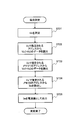
- FIG. 21 is a flowchart for explaining the self-test in the present embodiment
- FIG. 22 is a flowchart for explaining current measurement in the present embodiment.
- a current is passed through the calibration coil 52 (ST11), and the calibration voltage Vc and the detection resistance voltage Vs are measured via the AD converter (ST12).
- the numerical value of the calibration voltage Vc is stored as Vs ′ at the address specified by the detection resistance voltage Vs of the external memory 1 (ST13).
- this is repeated by changing the current up to the maximum value of the feedback current, and a table of the detection resistance voltage Vs and the calibration voltage Vc is created (ST14). By using this table, the detection resistance voltage Vs of the magnetic balanced current sensor can be calibrated.
- the detection resistance voltage Vs by the current detection resistance Rs1 is read through the AD converter (ST21), and the correction table stored in the external memory 1 is referred to based on the detection resistance voltage Vs, and correction is performed.
- Iin stored in the external memory 2 is read based on the corrected value Vs ′ with reference to a table for obtaining the measured current from the feedback current (ST24), and the read value is read from the sensor.
- the current value is output (ST25).
- the magnetoresistive effect element can be calibrated. Therefore, the output of the magnetoresistive effect element with respect to the input current is influenced by an external magnetic field or for some reason. Even if changes, current measurement can be performed with no measurement error.
- the present invention is not limited to the first to third embodiments, and can be implemented with various modifications.
- the materials, connection relations, thicknesses, sizes, manufacturing methods, and the like in Embodiments 1 to 3 can be changed as appropriate.
- the present invention can be implemented with appropriate modifications without departing from the scope of the present invention.
- the present invention can be applied to a current sensor that detects the magnitude of a current for driving a motor of an electric vehicle.
Landscapes
- Physics & Mathematics (AREA)
- General Physics & Mathematics (AREA)
- Chemical & Material Sciences (AREA)
- Engineering & Computer Science (AREA)
- Nanotechnology (AREA)
- Condensed Matter Physics & Semiconductors (AREA)
- Crystallography & Structural Chemistry (AREA)
- Measuring Instrument Details And Bridges, And Automatic Balancing Devices (AREA)
- Hall/Mr Elements (AREA)
Abstract
La présente invention concerne un capteur de courant à équilibre magnétique qui permet d'économiser de l'électricité et qui peut réduire l'influence des champs magnétiques externes. Ledit capteur de courant à équilibre magnétique est équipé : d'un élément magnétorésistant dont la résistance change en fonction de l'application d'un champ magnétique induit à partir du courant à mesurer ; d'une bobine de rétroaction qui est disposée au voisinage de l'élément magnétorésistant et qui génère un champ magnétique d'annulation qui annule le champ magnétique induit susmentionné ; d'un circuit en pont de détection de champ magnétique doté de deux sorties qui produisent une différence de tension correspondant au champ magnétique induit ; et d'un blindage magnétique qui atténue le champ magnétique induit et améliore le champ magnétique d'annulation susmentionné. Le courant à mesurer est mesuré sur la base d'un courant qui circule par la bobine de rétroaction lorsqu'un état équilibré est atteint, le champ magnétique induit et le champ magnétique d'annulation s'annulant. Le capteur de courant à équilibre magnétique est caractérisé en ce que la bobine de rétroaction, le blindage magnétique et le circuit en pont de détection de champ magnétique sont formés sur le même substrat.
Priority Applications (3)
| Application Number | Priority Date | Filing Date | Title |
|---|---|---|---|
| JP2011518588A JP5250109B2 (ja) | 2009-06-12 | 2010-06-11 | 磁気平衡式電流センサ |
| EP10786249.2A EP2442118B1 (fr) | 2009-06-12 | 2010-06-11 | Capteur de courant à équilibre magnétique |
| US13/300,064 US8754642B2 (en) | 2009-06-12 | 2011-11-18 | Magnetic balance type current sensor |
Applications Claiming Priority (2)
| Application Number | Priority Date | Filing Date | Title |
|---|---|---|---|
| JP2009-141706 | 2009-06-12 | ||
| JP2009141706 | 2009-06-12 |
Related Child Applications (1)
| Application Number | Title | Priority Date | Filing Date |
|---|---|---|---|
| US13/300,064 Continuation US8754642B2 (en) | 2009-06-12 | 2011-11-18 | Magnetic balance type current sensor |
Publications (1)
| Publication Number | Publication Date |
|---|---|
| WO2010143718A1 true WO2010143718A1 (fr) | 2010-12-16 |
Family
ID=43308973
Family Applications (1)
| Application Number | Title | Priority Date | Filing Date |
|---|---|---|---|
| PCT/JP2010/059959 Ceased WO2010143718A1 (fr) | 2009-06-12 | 2010-06-11 | Capteur de courant à équilibre magnétique |
Country Status (4)
| Country | Link |
|---|---|
| US (1) | US8754642B2 (fr) |
| EP (1) | EP2442118B1 (fr) |
| JP (1) | JP5250109B2 (fr) |
| WO (1) | WO2010143718A1 (fr) |
Cited By (15)
| Publication number | Priority date | Publication date | Assignee | Title |
|---|---|---|---|---|
| WO2012081377A1 (fr) * | 2010-12-16 | 2012-06-21 | アルプス電気株式会社 | Capteur magnétique et son procédé de fabrication |
| WO2012090631A1 (fr) * | 2010-12-27 | 2012-07-05 | アルプス・グリーンデバイス株式会社 | Capteur de courant proportionnel électromagnétique |
| WO2012093556A1 (fr) * | 2011-01-05 | 2012-07-12 | アルプス・グリーンデバイス株式会社 | Capteur de courant d'équilibre magnétique et procédé de fabrication d'un capteur de courant d'équilibre magnétique |
| WO2012120940A1 (fr) * | 2011-03-07 | 2012-09-13 | アルプス電気株式会社 | Capteur de courant |
| JP2013047610A (ja) * | 2011-08-28 | 2013-03-07 | Denso Corp | 磁気平衡式電流センサ |
| CN104040362A (zh) * | 2012-01-12 | 2014-09-10 | 阿尔卑斯绿色器件株式会社 | 电流传感器 |
| JP2014532883A (ja) * | 2011-11-11 | 2014-12-08 | 江▲蘇▼多▲維▼科技有限公司Jiang Su Multi Dimension Technology Co.,Ltd | 2重目的のリセットおよび較正コイルを有する磁力計 |
| WO2015119087A1 (fr) * | 2014-02-06 | 2015-08-13 | 株式会社寺田電機製作所 | Compteur de courant continu et procédé d'étalonnage de capteur de courant |
| JP2018112481A (ja) * | 2017-01-12 | 2018-07-19 | アルプス電気株式会社 | 磁気センサ |
| JP2018159692A (ja) * | 2017-03-24 | 2018-10-11 | Tdk株式会社 | 磁気センサ |
| DE102018114015A1 (de) | 2017-06-13 | 2018-12-13 | Tdk Corporation | Stromsensor |
| JP2019138807A (ja) * | 2018-02-13 | 2019-08-22 | アルプスアルパイン株式会社 | 磁気センサおよび電流センサ |
| JP2019148475A (ja) * | 2018-02-27 | 2019-09-05 | Tdk株式会社 | 磁気センサ |
| CN112230043A (zh) * | 2020-10-10 | 2021-01-15 | 浙江巨磁智能技术有限公司 | 一种利用磁平衡原理分离交直流的方法 |
| JP2024101562A (ja) * | 2023-01-17 | 2024-07-29 | リテルフューズ、インコーポレイテッド | 診断特徴を有する電流センサ |
Families Citing this family (22)
| Publication number | Priority date | Publication date | Assignee | Title |
|---|---|---|---|---|
| WO2011111493A1 (fr) | 2010-03-12 | 2011-09-15 | アルプス・グリーンデバイス株式会社 | Capteur de courant |
| WO2011111648A1 (fr) | 2010-03-12 | 2011-09-15 | アルプス電気株式会社 | Capteur de magnétisme et capteur de courant à balance magnétique utilisant ledit capteur de magnétisme |
| WO2011155261A1 (fr) * | 2010-06-09 | 2011-12-15 | アルプス・グリーンデバイス株式会社 | Capteur de courant à équilibre magnétique |
| CN103069282B (zh) * | 2010-08-23 | 2015-06-03 | 阿尔卑斯绿色器件株式会社 | 磁平衡式电流传感器 |
| US9594130B2 (en) * | 2012-04-23 | 2017-03-14 | Hitachi Metals, Ltd. | Magnetic sensor device |
| US9279865B2 (en) * | 2012-05-09 | 2016-03-08 | Everspin Technologies, Inc. | Method and structure for testing and calibrating three axis magnetic field sensing devices |
| JP2014092526A (ja) * | 2012-11-07 | 2014-05-19 | Mitsubishi Electric Corp | 磁気検出装置 |
| EP3244217B1 (fr) * | 2013-10-17 | 2019-05-22 | Osaka City University | Appareil de mesure de courant électrique |
| KR101524560B1 (ko) * | 2013-12-24 | 2015-06-01 | 만도헬라일렉트로닉스(주) | 전류 센서 오프셋 보정장치 및 그 보정방법 |
| CN103645449B (zh) * | 2013-12-24 | 2015-11-25 | 江苏多维科技有限公司 | 一种用于高强度磁场的单芯片参考桥式磁传感器 |
| JP6199730B2 (ja) | 2013-12-25 | 2017-09-20 | 株式会社東芝 | 電流センサ及び電流センサモジュール |
| JP6415813B2 (ja) | 2013-12-25 | 2018-10-31 | 株式会社東芝 | 電流センサ、電流測定モジュール及びスマートメータ |
| EP3364197B1 (fr) * | 2015-10-14 | 2020-07-01 | Alps Alpine Co., Ltd. | Dispositif de détection de courant |
| JP6724459B2 (ja) * | 2016-03-23 | 2020-07-15 | Tdk株式会社 | 磁気センサ |
| DE102017004349A1 (de) | 2017-05-08 | 2018-11-08 | Tdk-Micronas Gmbh | Magnetfeldkompensationseinrichtung |
| JP6620796B2 (ja) * | 2017-07-28 | 2019-12-18 | Tdk株式会社 | オフセット推定装置および方法、磁気センサの補正装置ならびに電流センサ |
| JP6690617B2 (ja) | 2017-09-15 | 2020-04-28 | Tdk株式会社 | 磁気センサ装置および電流センサ |
| US11002806B2 (en) * | 2018-03-29 | 2021-05-11 | Asahi Kasei Microdevices Corporation | Magnetic field detection device |
| US20200003846A1 (en) * | 2018-07-02 | 2020-01-02 | Asahi Kasei Microdevices Corporation | Magnetic field measuring device, magnetic field measurement method, and recording medium having recorded thereon magnetic field measurement program |
| US10983179B2 (en) | 2018-07-02 | 2021-04-20 | Asahi Kasei Microdevices Corporation | Magnetic field measuring device, magnetic field measurement method, and recording medium having recorded thereon magnetic field measurement program |
| CN114217114B (zh) * | 2021-12-21 | 2023-04-14 | 江苏多维科技有限公司 | 一种电流传感器 |
| CN114355019A (zh) * | 2021-12-30 | 2022-04-15 | 江苏兴宙微电子有限公司 | 一种无磁芯闭环电流检测模块结构及封装方法 |
Citations (5)
| Publication number | Priority date | Publication date | Assignee | Title |
|---|---|---|---|---|
| JPH07318591A (ja) * | 1994-05-25 | 1995-12-08 | Toyo Commun Equip Co Ltd | 電流検出器 |
| JPH0815322A (ja) | 1994-06-30 | 1996-01-19 | Hioki Ee Corp | 電流センサ |
| JP2000516714A (ja) | 1996-08-16 | 2000-12-12 | ノンボラタイル エレクトロニクス,インコーポレイテッド | 磁流センサ |
| JP2004132790A (ja) * | 2002-10-09 | 2004-04-30 | Fuji Electric Holdings Co Ltd | 電流センサ |
| JP2008275321A (ja) * | 2007-04-25 | 2008-11-13 | Tdk Corp | 電流センサ |
Family Cites Families (41)
| Publication number | Priority date | Publication date | Assignee | Title |
|---|---|---|---|---|
| CH651701A5 (de) * | 1980-12-24 | 1985-09-30 | Landis & Gyr Ag | Kompensierter messwandler. |
| US5561368A (en) | 1994-11-04 | 1996-10-01 | International Business Machines Corporation | Bridge circuit magnetic field sensor having spin valve magnetoresistive elements formed on common substrate |
| JP3545074B2 (ja) | 1994-12-27 | 2004-07-21 | 独立行政法人 科学技術振興機構 | 半導体基板に集積される磁気検出素子及び磁気検出モジュール |
| US6429640B1 (en) * | 2000-08-21 | 2002-08-06 | The United States Of America As Represented By The Secretary Of The Air Force | GMR high current, wide dynamic range sensor |
| US6949927B2 (en) * | 2001-08-27 | 2005-09-27 | International Rectifier Corporation | Magnetoresistive magnetic field sensors and motor control devices using same |
| US6773515B2 (en) | 2002-01-16 | 2004-08-10 | Headway Technologies, Inc. | FeTa nano-oxide layer as a capping layer for enhancement of giant magnetoresistance in bottom spin valve structures |
| JP2004247021A (ja) | 2002-07-31 | 2004-09-02 | Sony Corp | 磁気抵抗効果型磁気ヘッド |
| US7204013B2 (en) | 2003-07-29 | 2007-04-17 | Seagate Technology Llc | Method of manufacturing a magnetoresistive sensor |
| JP4312204B2 (ja) | 2003-11-27 | 2009-08-12 | 株式会社日立国際電気 | 基板処理装置、基板保持具、及び半導体装置の製造方法 |
| ATE386949T1 (de) * | 2003-12-23 | 2008-03-15 | Nxp Bv | Hochempfindlicher magnetischer eingebauter stromsensor |
| US20050237676A1 (en) | 2004-04-26 | 2005-10-27 | Hitachi Global Storage Technologies | Fe seeded self-pinned sensor |
| US7446982B2 (en) | 2004-07-01 | 2008-11-04 | Hitachi Global Storage Technologies Netherlands B.V. | Pinning structure with trilayer pinned layer |
| JP2006032522A (ja) | 2004-07-14 | 2006-02-02 | Alps Electric Co Ltd | 交換結合膜と前記交換結合膜を用いた磁気検出素子 |
| TWI278650B (en) | 2004-09-28 | 2007-04-11 | Yamaha Corp | Magnetic sensor using giant magnetoresistive elements and method for manufacturing the same |
| US7777607B2 (en) | 2004-10-12 | 2010-08-17 | Allegro Microsystems, Inc. | Resistor having a predetermined temperature coefficient |
| US7504824B2 (en) | 2004-10-21 | 2009-03-17 | International Business Machines Corporation | Magnetic sensor with offset magnetic field |
| JP4105142B2 (ja) | 2004-10-28 | 2008-06-25 | Tdk株式会社 | 電流センサ |
| US7554775B2 (en) | 2005-02-28 | 2009-06-30 | Hitachi Global Storage Technologies Netherlands B.V. | GMR sensors with strongly pinning and pinned layers |
| US8068317B2 (en) | 2005-07-22 | 2011-11-29 | Hitachi Global Storage Technologies Netherlands B.V. | Magnetic tunnel transistor with high magnetocurrent |
| US7365535B2 (en) * | 2005-11-23 | 2008-04-29 | Honeywell International Inc. | Closed-loop magnetic sensor system |
| JP2007147460A (ja) | 2005-11-28 | 2007-06-14 | Denso Corp | 磁気平衡式電流センサ |
| JP4668818B2 (ja) | 2006-03-13 | 2011-04-13 | アルプス電気株式会社 | 磁気センサ |
| JP5007916B2 (ja) | 2006-03-28 | 2012-08-22 | 日立金属株式会社 | 磁気センサ |
| US20070297220A1 (en) | 2006-06-22 | 2007-12-27 | Masatoshi Yoshikawa | Magnetoresistive element and magnetic memory |
| JP4923896B2 (ja) | 2006-09-15 | 2012-04-25 | 富士通株式会社 | 交換結合膜及び磁気デバイス |
| US7729093B1 (en) | 2006-09-28 | 2010-06-01 | Headway Technologies, Inc. | Detection of magnetic beads using a magnetoresistive device together with ferromagnetic resonance |
| JP4798498B2 (ja) | 2006-12-14 | 2011-10-19 | 日立金属株式会社 | 磁気センサーおよび磁気エンコーダー |
| JP4788922B2 (ja) | 2007-05-07 | 2011-10-05 | Tdk株式会社 | 電流センサ |
| JP2008286739A (ja) | 2007-05-21 | 2008-11-27 | Mitsubishi Electric Corp | 磁界検出器及び回転角度検出装置 |
| JP2008306112A (ja) | 2007-06-11 | 2008-12-18 | Hitachi Metals Ltd | 磁気抵抗効果膜、磁気センサ及び回転角度検出装置 |
| US7639005B2 (en) | 2007-06-15 | 2009-12-29 | Advanced Microsensors, Inc. | Giant magnetoresistive resistor and sensor apparatus and method |
| JP4877095B2 (ja) * | 2007-06-25 | 2012-02-15 | Tdk株式会社 | 電流センサおよびその製造方法 |
| US7826182B2 (en) | 2007-07-23 | 2010-11-02 | Hitachi Global Storage Technologies Netherlands B.V. | Current-perpendicular-to-the-plane (CPP) magnetoresistive sensor with CoFeGe ferromagnetic layers |
| JP5244805B2 (ja) | 2007-09-03 | 2013-07-24 | アルプス電気株式会社 | 磁気検出装置 |
| JP4780117B2 (ja) | 2008-01-30 | 2011-09-28 | 日立金属株式会社 | 角度センサ、その製造方法及びそれを用いた角度検知装置 |
| US7965077B2 (en) | 2008-05-08 | 2011-06-21 | Everspin Technologies, Inc. | Two-axis magnetic field sensor with multiple pinning directions |
| JP2010014686A (ja) | 2008-07-07 | 2010-01-21 | Kohshin Electric Corp | 電流検知デバイスおよびその設置方法および電流センサ |
| EP2442117B1 (fr) | 2009-06-12 | 2021-11-17 | Alps Alpine Co., Ltd. | Capteur de courant à équilibre magnétique |
| WO2011043193A1 (fr) * | 2009-10-05 | 2011-04-14 | アルプス・グリーンデバイス株式会社 | Capteur de courant à compensation magnétique |
| WO2011111648A1 (fr) * | 2010-03-12 | 2011-09-15 | アルプス電気株式会社 | Capteur de magnétisme et capteur de courant à balance magnétique utilisant ledit capteur de magnétisme |
| JPWO2011111536A1 (ja) * | 2010-03-12 | 2013-06-27 | アルプス・グリーンデバイス株式会社 | 磁気平衡式電流センサ |
-
2010
- 2010-06-11 WO PCT/JP2010/059959 patent/WO2010143718A1/fr not_active Ceased
- 2010-06-11 JP JP2011518588A patent/JP5250109B2/ja active Active
- 2010-06-11 EP EP10786249.2A patent/EP2442118B1/fr active Active
-
2011
- 2011-11-18 US US13/300,064 patent/US8754642B2/en active Active
Patent Citations (5)
| Publication number | Priority date | Publication date | Assignee | Title |
|---|---|---|---|---|
| JPH07318591A (ja) * | 1994-05-25 | 1995-12-08 | Toyo Commun Equip Co Ltd | 電流検出器 |
| JPH0815322A (ja) | 1994-06-30 | 1996-01-19 | Hioki Ee Corp | 電流センサ |
| JP2000516714A (ja) | 1996-08-16 | 2000-12-12 | ノンボラタイル エレクトロニクス,インコーポレイテッド | 磁流センサ |
| JP2004132790A (ja) * | 2002-10-09 | 2004-04-30 | Fuji Electric Holdings Co Ltd | 電流センサ |
| JP2008275321A (ja) * | 2007-04-25 | 2008-11-13 | Tdk Corp | 電流センサ |
Non-Patent Citations (1)
| Title |
|---|
| See also references of EP2442118A4 |
Cited By (30)
| Publication number | Priority date | Publication date | Assignee | Title |
|---|---|---|---|---|
| JPWO2012081377A1 (ja) * | 2010-12-16 | 2014-05-22 | アルプス電気株式会社 | 磁気センサ及び磁気センサの製造方法 |
| WO2012081377A1 (fr) * | 2010-12-16 | 2012-06-21 | アルプス電気株式会社 | Capteur magnétique et son procédé de fabrication |
| WO2012090631A1 (fr) * | 2010-12-27 | 2012-07-05 | アルプス・グリーンデバイス株式会社 | Capteur de courant proportionnel électromagnétique |
| WO2012093556A1 (fr) * | 2011-01-05 | 2012-07-12 | アルプス・グリーンデバイス株式会社 | Capteur de courant d'équilibre magnétique et procédé de fabrication d'un capteur de courant d'équilibre magnétique |
| JPWO2012120940A1 (ja) * | 2011-03-07 | 2014-07-17 | アルプス電気株式会社 | 電流センサ |
| WO2012120940A1 (fr) * | 2011-03-07 | 2012-09-13 | アルプス電気株式会社 | Capteur de courant |
| JP2013047610A (ja) * | 2011-08-28 | 2013-03-07 | Denso Corp | 磁気平衡式電流センサ |
| US9599693B2 (en) | 2011-11-11 | 2017-03-21 | MultiDimension Technology Co., Ltd. | Magnetometer with dual purpose reset and calibration coil |
| JP2014532883A (ja) * | 2011-11-11 | 2014-12-08 | 江▲蘇▼多▲維▼科技有限公司Jiang Su Multi Dimension Technology Co.,Ltd | 2重目的のリセットおよび較正コイルを有する磁力計 |
| EP2790030A4 (fr) * | 2011-11-11 | 2016-01-20 | Multidimension Technology Co Ltd | Dispositif de détection de champ magnétique |
| CN104040362A (zh) * | 2012-01-12 | 2014-09-10 | 阿尔卑斯绿色器件株式会社 | 电流传感器 |
| JPWO2013105451A1 (ja) * | 2012-01-12 | 2015-05-11 | アルプス・グリーンデバイス株式会社 | 電流センサ |
| CN104040362B (zh) * | 2012-01-12 | 2016-05-04 | 阿尔卑斯绿色器件株式会社 | 电流传感器 |
| JPWO2015119087A1 (ja) * | 2014-02-06 | 2017-03-23 | 株式会社寺田電機製作所 | 直流電力量計および電流センサー校正方法 |
| WO2015119087A1 (fr) * | 2014-02-06 | 2015-08-13 | 株式会社寺田電機製作所 | Compteur de courant continu et procédé d'étalonnage de capteur de courant |
| JP2018112481A (ja) * | 2017-01-12 | 2018-07-19 | アルプス電気株式会社 | 磁気センサ |
| JP2018159692A (ja) * | 2017-03-24 | 2018-10-11 | Tdk株式会社 | 磁気センサ |
| US11892477B2 (en) | 2017-06-13 | 2024-02-06 | Tdk Corporation | Current sensor having soft magnetic bodies for adjusting magnetic field intensity |
| DE102018114015A1 (de) | 2017-06-13 | 2018-12-13 | Tdk Corporation | Stromsensor |
| JP2019002742A (ja) * | 2017-06-13 | 2019-01-10 | Tdk株式会社 | 電流センサ |
| US11293950B2 (en) | 2017-06-13 | 2022-04-05 | Tdk Corporation | Current sensor having soft magnetic bodies for adjusting magnetic field intensity |
| JP2019138807A (ja) * | 2018-02-13 | 2019-08-22 | アルプスアルパイン株式会社 | 磁気センサおよび電流センサ |
| JP7057680B2 (ja) | 2018-02-13 | 2022-04-20 | アルプスアルパイン株式会社 | 磁気センサおよび電流センサ |
| JP2019148475A (ja) * | 2018-02-27 | 2019-09-05 | Tdk株式会社 | 磁気センサ |
| WO2019167598A1 (fr) * | 2018-02-27 | 2019-09-06 | Tdk株式会社 | Capteur magnétique |
| JP7020176B2 (ja) | 2018-02-27 | 2022-02-16 | Tdk株式会社 | 磁気センサ |
| CN112230043A (zh) * | 2020-10-10 | 2021-01-15 | 浙江巨磁智能技术有限公司 | 一种利用磁平衡原理分离交直流的方法 |
| CN112230043B (zh) * | 2020-10-10 | 2023-12-08 | 浙江巨磁智能技术有限公司 | 一种利用磁平衡原理分离交直流的方法 |
| JP2024101562A (ja) * | 2023-01-17 | 2024-07-29 | リテルフューズ、インコーポレイテッド | 診断特徴を有する電流センサ |
| JP7889811B2 (ja) | 2023-01-17 | 2026-07-14 | リテルフューズ、インコーポレイテッド | 診断特徴を有する電流センサ |
Also Published As
| Publication number | Publication date |
|---|---|
| JP5250109B2 (ja) | 2013-07-31 |
| US20120062224A1 (en) | 2012-03-15 |
| JPWO2010143718A1 (ja) | 2012-11-29 |
| US8754642B2 (en) | 2014-06-17 |
| EP2442118A4 (fr) | 2017-06-21 |
| EP2442118A1 (fr) | 2012-04-18 |
| EP2442118B1 (fr) | 2021-11-10 |
Similar Documents
| Publication | Publication Date | Title |
|---|---|---|
| JP5250109B2 (ja) | 磁気平衡式電流センサ | |
| JP5572208B2 (ja) | 磁気センサ及びそれを用いた磁気平衡式電流センサ | |
| JP5411285B2 (ja) | 磁気平衡式電流センサ | |
| JP5594915B2 (ja) | 電流センサ | |
| JP5012939B2 (ja) | 電流センサ | |
| JP5250108B2 (ja) | 磁気平衡式電流センサ | |
| JP5487402B2 (ja) | 磁気平衡式電流センサ | |
| US20130057273A1 (en) | Current sensor | |
| JP5505817B2 (ja) | 磁気平衡式電流センサ | |
| US20120306491A1 (en) | Magnetic balance type current sensor | |
| JP7057680B2 (ja) | 磁気センサおよび電流センサ | |
| WO2017199519A1 (fr) | Dispositif de détection magnétique du type à équilibre | |
| WO2011111537A1 (fr) | Capteur de courant | |
| US12320869B2 (en) | Magnetic sensor and current sensor including magneto-resistance element | |
| JP7122836B2 (ja) | 磁気センサおよび電流センサ | |
| WO2020054112A1 (fr) | Capteur magnétique et capteur de courant |
Legal Events
| Date | Code | Title | Description |
|---|---|---|---|
| 121 | Ep: the epo has been informed by wipo that ep was designated in this application |
Ref document number: 10786249 Country of ref document: EP Kind code of ref document: A1 |
|
| WWE | Wipo information: entry into national phase |
Ref document number: 2011518588 Country of ref document: JP |
|
| NENP | Non-entry into the national phase |
Ref country code: DE |
|
| WWE | Wipo information: entry into national phase |
Ref document number: 2010786249 Country of ref document: EP |