WO2010143763A1 - Module laser réglable pour cavité externe - Google Patents
Module laser réglable pour cavité externe Download PDFInfo
- Publication number
- WO2010143763A1 WO2010143763A1 PCT/KR2009/003184 KR2009003184W WO2010143763A1 WO 2010143763 A1 WO2010143763 A1 WO 2010143763A1 KR 2009003184 W KR2009003184 W KR 2009003184W WO 2010143763 A1 WO2010143763 A1 WO 2010143763A1
- Authority
- WO
- WIPO (PCT)
- Prior art keywords
- optical waveguide
- light source
- bragg grating
- optical
- temperature sensor
- Prior art date
- Legal status (The legal status is an assumption and is not a legal conclusion. Google has not performed a legal analysis and makes no representation as to the accuracy of the status listed.)
- Ceased
Links
Images


Classifications
-
- H—ELECTRICITY
- H01—ELECTRIC ELEMENTS
- H01S—DEVICES USING THE PROCESS OF LIGHT AMPLIFICATION BY STIMULATED EMISSION OF RADIATION [LASER] TO AMPLIFY OR GENERATE LIGHT; DEVICES USING STIMULATED EMISSION OF ELECTROMAGNETIC RADIATION IN WAVE RANGES OTHER THAN OPTICAL
- H01S5/00—Semiconductor lasers
- H01S5/10—Construction or shape of the optical resonator, e.g. extended or external cavity, coupled cavities, bent-guide, varying width, thickness or composition of the active region
- H01S5/14—External cavity lasers
- H01S5/141—External cavity lasers using a wavelength selective device, e.g. a grating or etalon
-
- H—ELECTRICITY
- H01—ELECTRIC ELEMENTS
- H01S—DEVICES USING THE PROCESS OF LIGHT AMPLIFICATION BY STIMULATED EMISSION OF RADIATION [LASER] TO AMPLIFY OR GENERATE LIGHT; DEVICES USING STIMULATED EMISSION OF ELECTROMAGNETIC RADIATION IN WAVE RANGES OTHER THAN OPTICAL
- H01S3/00—Lasers, i.e. devices using stimulated emission of electromagnetic radiation in the infrared, visible or ultraviolet wave range
- H01S3/10—Controlling the intensity, frequency, phase, polarisation or direction of the emitted radiation, e.g. switching, gating, modulating or demodulating
-
- H—ELECTRICITY
- H01—ELECTRIC ELEMENTS
- H01S—DEVICES USING THE PROCESS OF LIGHT AMPLIFICATION BY STIMULATED EMISSION OF RADIATION [LASER] TO AMPLIFY OR GENERATE LIGHT; DEVICES USING STIMULATED EMISSION OF ELECTROMAGNETIC RADIATION IN WAVE RANGES OTHER THAN OPTICAL
- H01S3/00—Lasers, i.e. devices using stimulated emission of electromagnetic radiation in the infrared, visible or ultraviolet wave range
- H01S3/05—Construction or shape of optical resonators; Accommodation of active medium therein; Shape of active medium
- H01S3/06—Construction or shape of active medium
- H01S3/063—Waveguide lasers, i.e. whereby the dimensions of the waveguide are of the order of the light wavelength
- H01S3/067—Fibre lasers
-
- H—ELECTRICITY
- H01—ELECTRIC ELEMENTS
- H01S—DEVICES USING THE PROCESS OF LIGHT AMPLIFICATION BY STIMULATED EMISSION OF RADIATION [LASER] TO AMPLIFY OR GENERATE LIGHT; DEVICES USING STIMULATED EMISSION OF ELECTROMAGNETIC RADIATION IN WAVE RANGES OTHER THAN OPTICAL
- H01S5/00—Semiconductor lasers
- H01S5/02—Structural details or components not essential to laser action
- H01S5/022—Mountings; Housings
- H01S5/02208—Mountings; Housings characterised by the shape of the housings
- H01S5/02212—Can-type, e.g. TO-CAN housings with emission along or parallel to symmetry axis
-
- H—ELECTRICITY
- H01—ELECTRIC ELEMENTS
- H01S—DEVICES USING THE PROCESS OF LIGHT AMPLIFICATION BY STIMULATED EMISSION OF RADIATION [LASER] TO AMPLIFY OR GENERATE LIGHT; DEVICES USING STIMULATED EMISSION OF ELECTROMAGNETIC RADIATION IN WAVE RANGES OTHER THAN OPTICAL
- H01S5/00—Semiconductor lasers
- H01S5/02—Structural details or components not essential to laser action
- H01S5/022—Mountings; Housings
- H01S5/0225—Out-coupling of light
- H01S5/02251—Out-coupling of light using optical fibres
-
- H—ELECTRICITY
- H01—ELECTRIC ELEMENTS
- H01S—DEVICES USING THE PROCESS OF LIGHT AMPLIFICATION BY STIMULATED EMISSION OF RADIATION [LASER] TO AMPLIFY OR GENERATE LIGHT; DEVICES USING STIMULATED EMISSION OF ELECTROMAGNETIC RADIATION IN WAVE RANGES OTHER THAN OPTICAL
- H01S5/00—Semiconductor lasers
- H01S5/02—Structural details or components not essential to laser action
- H01S5/022—Mountings; Housings
- H01S5/0225—Out-coupling of light
- H01S5/02253—Out-coupling of light using lenses
-
- H—ELECTRICITY
- H01—ELECTRIC ELEMENTS
- H01S—DEVICES USING THE PROCESS OF LIGHT AMPLIFICATION BY STIMULATED EMISSION OF RADIATION [LASER] TO AMPLIFY OR GENERATE LIGHT; DEVICES USING STIMULATED EMISSION OF ELECTROMAGNETIC RADIATION IN WAVE RANGES OTHER THAN OPTICAL
- H01S5/00—Semiconductor lasers
- H01S5/02—Structural details or components not essential to laser action
- H01S5/024—Arrangements for thermal management
- H01S5/02407—Active cooling, e.g. the laser temperature is controlled by a thermo-electric cooler or water cooling
- H01S5/02415—Active cooling, e.g. the laser temperature is controlled by a thermo-electric cooler or water cooling by using a thermo-electric cooler [TEC], e.g. Peltier element
-
- H—ELECTRICITY
- H01—ELECTRIC ELEMENTS
- H01S—DEVICES USING THE PROCESS OF LIGHT AMPLIFICATION BY STIMULATED EMISSION OF RADIATION [LASER] TO AMPLIFY OR GENERATE LIGHT; DEVICES USING STIMULATED EMISSION OF ELECTROMAGNETIC RADIATION IN WAVE RANGES OTHER THAN OPTICAL
- H01S5/00—Semiconductor lasers
- H01S5/02—Structural details or components not essential to laser action
- H01S5/024—Arrangements for thermal management
- H01S5/02438—Characterized by cooling of elements other than the laser chip, e.g. an optical element being part of an external cavity or a collimating lens
- H01S5/02446—Cooling being separate from the laser chip cooling
-
- H—ELECTRICITY
- H01—ELECTRIC ELEMENTS
- H01S—DEVICES USING THE PROCESS OF LIGHT AMPLIFICATION BY STIMULATED EMISSION OF RADIATION [LASER] TO AMPLIFY OR GENERATE LIGHT; DEVICES USING STIMULATED EMISSION OF ELECTROMAGNETIC RADIATION IN WAVE RANGES OTHER THAN OPTICAL
- H01S5/00—Semiconductor lasers
- H01S5/02—Structural details or components not essential to laser action
- H01S5/028—Coatings ; Treatment of the laser facets, e.g. etching, passivation layers or reflecting layers
- H01S5/0287—Facet reflectivity
-
- H—ELECTRICITY
- H01—ELECTRIC ELEMENTS
- H01S—DEVICES USING THE PROCESS OF LIGHT AMPLIFICATION BY STIMULATED EMISSION OF RADIATION [LASER] TO AMPLIFY OR GENERATE LIGHT; DEVICES USING STIMULATED EMISSION OF ELECTROMAGNETIC RADIATION IN WAVE RANGES OTHER THAN OPTICAL
- H01S5/00—Semiconductor lasers
- H01S5/10—Construction or shape of the optical resonator, e.g. extended or external cavity, coupled cavities, bent-guide, varying width, thickness or composition of the active region
- H01S5/1003—Waveguide having a modified shape along the axis, e.g. branched, curved, tapered, voids
Definitions
- the present invention relates to an external resonant wavelength tunable optical module that can be manufactured through mature semiconductor process technology, can stably and accurately change wavelengths, and has excellent long-term reliability and reproducibility of oscillation wavelength when wavelength is varied.
- WDM Widelength Division Multiplexing
- WDM-based passive optical networks are increasingly attracting attention as a way to increase communication bandwidth in a subscriber network.
- the communication between the central base station and the subscriber is performed by using each wavelength determined for each subscriber, so that a dedicated wavelength is used for each subscriber. Therefore, the WDM-PON is excellent in security, It is possible to apply different transmission techniques (for example, link rate, frame format, etc.).
- WDM-PON is a technique of multiplexing multiple wavelengths in a single optical fiber using WDM technology
- a WDM-PON requires a light source of different wavelengths corresponding to the number of subscribers belonging to one RN (Remote Node).
- the wavelength tunable semiconductor laser can be classified into a single integrated laser such as a Distributed FeedBack (DFB) laser or a DBR (Distributed Bragg reflector) laser and an external cavity laser (ECL).
- EDL external cavity laser
- the oscillation wavelength of the DFB laser is determined by the period of the grating and the effective refractive index
- the oscillation wavelength can be controlled by using the thermo-optic effect in which the refractive index is changed by heat.
- the relative temperature that can be applied to the device is very limited and has a wavelength tuning range of 10 nm or less.
- the wavelength variable range is broader and the control speed is faster than that of the DFB laser which is controlled thermally.
- an optical amplifier since an optical amplifier has to be further integrated to compensate absorption loss due to a free carrier applied to the Bragg grating region and the fabrication process is very complicated, it is not suitable as a low-cost light source.
- the external resonant laser is formed by the optical coupling of the optical gain medium such as a reflective optical amplifier or a laser diode (LD) and a wavelength-selective reflection filter such as a fiber Bragg grating or a flat waveguide Bragg grating,
- the optical gain medium such as a reflective optical amplifier or a laser diode (LD)
- LD laser diode
- the oscillation wavelength is determined by the wavelength.
- the reflection wavelength of the fiber Bragg grating or waveguide Bragg grating is determined by the grating period and the effective refractive index of the waveguide, it is possible to control the reflection wavelength using a thermooptic effect in which the refractive index is changed by heat.
- thermo-optic coefficient of the silica which is the material of the optical fiber
- the thermo-optic coefficient of the silica is about 1.1 x 10 -5 / K
- the reflected wave length of the fiber Bragg grating has a very small temperature dependency of about 0.01 nm / K. Therefore, a method of mechanically pulling a fiber Bragg grating to change the grating period is used. In this wavelength tunable method, the fiber Bragg grating is easily damaged by physical stress, and the tunable range is not large.
- the polymer-based waveguide grating lattice has a thermo-optic coefficient of about -1 x 10 -4 / K to -3 x 10 -4 / K, which is ten times higher than that of silica. Or more.
- a polymer optical waveguide-based external resonant wavelength tunable laser uses a metal thin film heating element at the top of the optical waveguide to vary the refractive index of the polymer by varying the refractive index of the polymer, and a thermoelectric cooler A temperature controller consisting of a temperature sensor is used.
- the temperature gradient between the heating element and the thermoelectric cooler increases and local stress is applied to the waveguide in the heating element region.
- thermo-optic effect causes degradation of the polymer material due to heat applied to the polymer material for a long time, In particular, it is very difficult to secure the stability required for a WDM optical communication system at intervals of 100 GHz.
- the change of the effective refractive index of the waveguide due to the above causes not only the wavelength control required by the WDM optical communication system but also limits the wavelength tuning range.
- An object of the present invention is to provide an external resonant wavelength tunable laser module that is manufactured based on mature silicon semiconductor processes and has high production yield, low cost, and mass production capability.
- the present invention provides an external resonant tunable laser module having high stability and reproducibility and high thermal / optical / mechanical stability and durability. It is independent of external heat environment, has high optical coupling efficiency, and can stably change wavelength in a short time And an outer resonance type tunable laser module.
- An external resonant tunable laser module includes: a light source for generating broadband light; A semiconductor optical waveguide whose one end is optically coupled with the light source; A Bragg grating formed on the optical waveguide; A thin film heater provided on the Bragg grating and controlling a reflection band of the Bragg grating by a thermo-optic effect; A first temperature sensor provided on the optical waveguide; A thermo-electric cooler (TEC) provided under the optical waveguide; A heat insulating layer provided between the optical waveguide and the thermoelectric cooler; And an optical fiber optically coupled to the other end of the optical waveguide.
- TEC thermo-electric cooler
- the light source is a TO-CAN packaged light source that includes a semiconductor laser diode chip that generates light and a photodiode that detects the intensity of the generated light.
- the light source and the semiconductor optical waveguide are optically coupled And the optical lens is integrally attached to the light source packaged with the TiO2 can (TO-CAN).
- the external resonant tunable laser module further includes a second temperature sensor, and the second temperature sensor is provided between the heat insulating layer and the thermoelectric cooler.
- the light source includes a semiconductor laser diode chip for generating a broadband light in which a spot size converter is integrated, and a photodiode for detecting the intensity of the generated light are mounted on a sub-mount
- the light source is provided on the thermoelectric cooler, the light source and the optical waveguide are optically coupled by butt coupling, and a metal layer is provided between the light source and the thermoelectric cooler.
- the external resonant tunable laser module further includes a second temperature sensor, and the second temperature sensor is provided between the metal layer and the thermoelectric cooler.
- the external resonant tunable laser module further comprises an optical fiber support for supporting an optical fiber, wherein the light source, the optical waveguide formed with a Bragg grating, the thin film heater, the first temperature sensor, the thermoelectric cooler, Is provided in the single housing, and the optical fiber is fixed to the housing by the optical fiber support.
- the optical coupling between the optical waveguide and the optical fiber is characterized by lens coupling or butt coupling by an optical lens.
- the optical waveguide and the optical fiber are optically coupled by butt-coupling, and the optical fiber is a lens-type optical fiber.
- the optical waveguide is formed on a silicon-on-insulator (SOI) substrate including a lower silicon layer, a buried silicon oxide layer, and an upper silicon layer, A lower clad as said buried silicon oxide layer; Air or silicon oxide, and the Bragg grating is formed by selective etching of the silicon core, and the Bragg grating is formed of air or silicon oxide.
- SOI silicon-on-insulator
- the optical waveguide is a channel type, a rib type or a ridge type silicon optical waveguide
- the Bragg grating is a structure in which one or more Bragg gratings are connected in series, Independently of one another, are primary, tertiary, fifth, or n (odd numbered n > 5) Bragg gratings.
- the insulating layer is glass and the metal layer is Al or Cu with high thermal conductivity.
- the external resonant tunable laser module may further include a controller, wherein the controller receives the outputs of the first temperature sensor and the second temperature sensor, respectively, and controls the voltage applied to the thermoelectric cooler and the thin film heater, The current can be controlled.
- the external resonant tunable laser module according to the present invention is advantageous in that it can obtain a stable, reproducible and reliable oscillation wavelength by using a wavelength tunable filter based on a semiconductor material, and by using a temperature locking function using a temperature sensor and a thermoelectric cooler , It is possible to fabricate a tunable laser module by using a mature semiconductor process, resulting in a high production yield and a low cost.
- Characteristic of the SOI-based silicon optical waveguide is that the wavelength stability and reproducibility And the wavelength can be varied with high reliability even for a long time.
- the optical module including the optical module including the light source, the Bragg grating, the thin film heater, the first temperature sensor, the thermoelectric cooler, and the second temperature sensor is provided in a single housing, the thermal / mechanical stability and high durability .
- the external resonant tunable laser module according to the present invention is advantageous in that it can obtain a stable, reproducible and reliable oscillation wavelength by using a wavelength tunable filter based on a semiconductor material, and by using a temperature locking function using a temperature sensor and a thermoelectric cooler , It is possible to fabricate a tunable laser module by using a mature semiconductor process, resulting in high production yield and low cost.
- Characteristic of the SOI-based silicon optical waveguide is that the wavelength stability and reproducibility And the wavelength can be varied with high reliability even for a long time.
- the optical module including the optical module including the light source, the Bragg grating, the thin film heater, the first temperature sensor, the thermoelectric cooler, and the second temperature sensor is provided in a single housing, the thermal / mechanical stability and high durability .
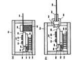
- FIG. 1 is a structure of an external resonance type tunable laser module according to the present invention
- FIG. 2 shows a structure of a silicon waveguide Bragg grating using an SOI substrate as an example of a semiconductor waveguide Bragg grating of the present invention
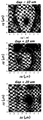
- FIG. 4 is a graphical representation of the reflectivity and reflection band of the etched depth of the silicon waveguide brick grid of the present invention
- optical fiber and the optical waveguide are an example of the butt coupling (FIG. 5A) or the optical coupling by the lens (FIG. 5B)
- FIG. 6 is a graphical representation of the relative temperature of the optical waveguide region according to the thermal characteristics of the heat insulating substrate provided in the external resonant tunable laser module according to the present invention
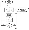
- FIG. 7 illustrates a temperature control algorithm of the external resonant tunable laser module according to the present invention
- FIG. 8 shows another example of the external resonant tunable laser module according to the present invention, in which the optical fiber and the optical waveguide are an example of the butt coupling (FIG. 8A) or the optical coupling by the lens (FIG. 8B)
- FIG. 9 is a graph illustrating the optical coupling efficiency according to the distance between the light source and the optical waveguide during the optical coupling by the butt coupling between the light source and the optical waveguide in the example of the external resonant tunable laser module according to the present invention.
- thermoelectric cooler 111 second temperature sensor
- first temperature sensor 511 housing
- insulating layer 512 metal layer
- the external resonant tunable laser module includes a light source for outputting multi-wavelength light in a wide band, a semiconductor optical waveguide, a Bragg grating formed on the semiconductor optical waveguide, a thin film heater disposed above the optical waveguide formed with the Bragg grating a heater, a first temperature sensor, a thermo-electric cooler (TEC), and an optical fiber, and more particularly, a second temperature sensor.
- a light source for outputting multi-wavelength light in a wide band
- a semiconductor optical waveguide for outputting multi-wavelength light in a wide band
- a Bragg grating formed on the semiconductor optical waveguide
- a thin film heater disposed above the optical waveguide formed with the Bragg grating a heater
- TEC thermo-electric cooler
- an optical fiber and more particularly, a second temperature sensor.
- the light source is optically coupled to one end of the semiconductor optical waveguide formed with the Bragg grating to constitute an external resonator and a reflection wavelength band of the Bragg grating is adjusted using a thermo-optic effect by the thin film heater, And the oscillation wavelength is outputted by resonance through the optical fiber optically coupled with the other stage.
- the first temperature sensor is located above the semiconductor optical waveguide and measures the temperature of the optical waveguide in real time for realizing a precise and stable wavelength-locking function, and controls the current applied to the thin film heater It is for this reason.
- thermoelectric cooler is disposed under the semiconductor optical waveguide so as to control the amount of heat generated by the power applied to the thin film heater to produce a precise thermooptical effect irrespective of the external environmental temperature of the external resonant tunable laser module, And a second temperature sensor for precisely controlling the heat absorbing amount of the cooler is located above the thermoelectric cooler.
- the broadband light emitted from the light source is input to the core of the semiconductor optical waveguide by optical coupling, and the light having a wavelength that is reflected by the Bragg grating formed on the semiconductor optical waveguide is input to the emission surface of the light source
- the oscillation wavelength having the central wavelength of the reflection band of the Bragg grating is obtained.
- the second temperature sensor is provided between the semiconductor optical waveguide and the thermoelectric cooler, or the light source is located above the thermoelectric cooler and the second temperature sensor is located between the light source and the thermoelectric cooler.
- optical coupling between the light source and the semiconductor optical waveguide is performed by coupling or butt coupling by an optical lens (optical coupling lens), and optical coupling between the semiconductor optical waveguide and the optical fiber is performed by the light source and the semiconductor optical waveguide (Optical coupling lens) or butt coupling independent of the optical coupling type of the optical lens.
- optical lens optical coupling lens
- the thin film heater is Joule heat as a predetermined electric signal applied to the thin metal film (Joule heat) the generated and varying the temperature of the semiconductor optical waveguide with a Bragg grating is formed, open-optic effect (craze academia of the semiconductor optical waveguide ⁇ 1x10 - 4 / ⁇ ⁇ ) to adjust the reflection wavelength band reflected from the Bragg grating.
- the first temperature sensor or the second temperature sensor may include a device used in a conventional temperature sensor in which a voltage, a resistance, or an amount of current is changed by heat.
- the first temperature sensor or the second temperature sensor may include a thermistor .
- the thermoelectric cooler may include a conventional thermoelectric element in which heat is absorbed by a predetermined electrical signal.
- the light source is a semiconductor optical amplifier or a semiconductor laser diode chip.
- the outgoing surface of the light has an anti-reflection (AR) coating of 1% or less and an opposite surface of the emitting surface has a high- reflection, less HR) coating.
- AR anti-reflection
- the light source is a semiconductor laser diode chip for broadband wavelength oscillation, which includes an active layer, a current blocking layer, a p-metal layer and a p-metal layer for generating light, InGaAsP, InGaAlAs, and InAlAs, or a combination of Group 2-4 elements on the InP substrate.
- the active layer may be a multi-quantum-well structure or a bulk active structure. .
- the optical waveguide in which the Bragg grating is formed may be formed of a III-V material such as silicon or indium phosphide (InP) using a silicon on insulator (SOI) substrate including a lower silicon layer, a buried silicon oxide layer, Group element, and the optical waveguide core is preferably a geometric channel structure, a rib or a ridge structure.
- a III-V material such as silicon or indium phosphide (InP) using a silicon on insulator (SOI) substrate including a lower silicon layer, a buried silicon oxide layer, Group element, and the optical waveguide core is preferably a geometric channel structure, a rib or a ridge structure.
- the Bragg grating is fabricated by forming a groove having a constant period in the traveling direction of the light in the semiconductor optical waveguide.
- the cavity (air) of the groove forms a Bragg grating, or a waveguide core such as silicon oxide,
- a different material with a lower refractive index than the material can be filled to form a Bragg grating. It is preferable that the lattice order of the Bragg grating has an odd order degree of first order or higher.
- the light source may be optically coupled to the semiconductor optical waveguide by active alignment in a TO-CAN packaged form in which an optical coupling lens is integrally mounted, and the light source and the semiconductor optical waveguide May be optically coupled via a light coupling lens or a butt optical coupling.
- NA values on the light source side and the semiconductor optical waveguide side preferably have the same values as the NA values of the light source and the optical waveguide, respectively, and AR coating is preferably applied to each surface.
- the semiconductor optical waveguide satisfies Snell's law and the traveling direction of light traveling in a free space between the light source and the semiconductor optical waveguide in order to increase coupling efficiency when the light source and the semiconductor optical waveguide are optically coupled to each other And is tilted at an angle that is equal to or greater than a predetermined angle.
- the tilt includes a tilt of a partial region including a light incident surface of the semiconductor optical waveguide and a tilt of the entire semiconductor optical waveguide.
- the core of the optical waveguide is preferably formed at an angle that satisfies Snell's law for the angle of incidence of light with respect to the light incident surface.
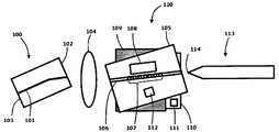
- a light source 100 and a tunable filter 120 for generating light of a plurality of wavelengths in a wide band are optically coupled by an optically coupled lens 104 to form a light path from the back surface 103 of the light source 100 to the wavelength tunable filter
- the Bragg grating 107 formed on the semiconductor optical waveguide 106 of the semiconductor optical waveguide 120 forms a resonator so that light corresponding to the reflection wavelength of the Bragg grating 113 resonates and oscillates, 113, respectively.
- the exit surface 102 of the light source 100 is AR coated to a 1% or less AR coating to suppress Fabry-Perot (FP) mode oscillation due to reflection at the exit surface 102,
- the HR coating has a reflectance of 80% or more.
- the optical waveguide region 101 of the light source 100 is composed of a passive optical waveguide optically coupled with a photoactive layer or a photoactive layer so as to reduce the reflection at the exit face 102, And it is preferable to be formed so as to be perpendicular to the back surface 103 to obtain a high reflectivity.
- An AR coating having a reflectance of 1% or less is formed on both surfaces of the optical coupling lens 104 to prevent light output from the light source 100 or light reflected from the Bragg grating 113 from being reflected from the lens surface desirable.
- the optical coupling lens 104 is an aspherical lens.
- the numerical aperture (NA) value on the light source side has a value similar to the NA value of the light source 100, It is preferable that the value has a value similar to the NA value of the optical waveguide.
- the optical fiber 113 is preferably a lens-shaped optical fiber or an inclined surface having a cross section of 4 degrees or more and is tilted so as to satisfy the Snell's law and has an AR coating of 1% or less.
- the wavelength tunable filter 120 forms a waveguide core 106 on which light travels through total internal reflection on a semiconductor substrate 105 and forms a groove having a constant period in a direction in which light travels on the core And a Bragg grating 107 is manufactured.
- the periodic grooves impart periodic perturbations to the refractive index of the waveguide on which the light travels.
- the wavelength (? B ) reflected by the Bragg grating is determined by the lattice equation (1).
- n eff is the effective refractive index of the optical waveguide
- A is the period of the Bragg grating
- Equation (2) the change of the Bragg reflection wavelength with temperature is derived as shown in Equation (2).
- M, n eff and? are the same as in Equation 1, and? 0 is the initial reflection wavelength. That is, the amount of change of the reflected wavelength with respect to temperature is proportional to the sum of the change amount of the effective refractive index with respect to temperature and the change amount of the grating period. For example, assuming a lattice order, m, of 1 and a silicon waveguide Bragg grating with an initial wavelength ⁇ 0 of 1550 nm, the change in the reflected wavelength with respect to temperature is 0.085 nm / K with a 12 nm variable It can be seen that the temperature is about 142K. In this example, the thermo-optic coefficient of the silicon, DELTA n eff / DELTA T was 1.9 x 10 < -4 > / K and the change in the period due to temperature was ignored.
- a thin film heater 108 including a heating element in the form of a metal thin film is preferably provided on the semiconductor substrate 105.
- the heating element is formed by depositing a metal material such as Cr, Au, Ni, Ni / Cr, or TiW to an appropriate thickness.
- a regulating device is provided.
- a heat insulating layer 109 is provided between the semiconductor substrate 105 and the thermoelectric cooler 110 to minimize the power consumption of the heat generating body.
- a first temperature sensor 112 for monitoring the temperature applied to the Bragg grating 107 in real time and for regulating the current applied to the heating element is mounted on the semiconductor substrate 105.
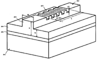
- FIG. 2 is a structural view of a silicon waveguide Bragg grating using a silicon-on-insulator (SOI) substrate 201 as an example of the wavelength tunable filter 120.
- SOI silicon-on-insulator
- the geometrical structure of the optical waveguide is composed of a lip region 203 and a slab region 204 in a lipped waveguide structure.
- the lips waveguide 202 is formed in the upper silicon region of the SOI substrate 201.
- an insulating layer 205 which is a buried silicon oxide layer formed under the lip waveguide 202, and an upper air layer or a covering layer having a lower refractive index than silicon, (Not shown), and in the horizontal direction, light confinement and loss-free propagation are possible due to the difference in effective refractive index by the lip region 203.
- the lip waveguide 202 becomes a single mode condition when the relationship between the width W of the lip region 203, the height H and the height h of the slab region 203 satisfies the following expression (3) .
- r is a ratio (h / H) of the slab area 203 with respect to the lip area 202 to a value greater than 0.5 and less than 1, and a height H of the lip area should satisfy the constraint as shown in equation (4).
- Equation 4 ⁇ is the wavelength of light in free space, and n Si and n SiO2 are the refractive indices of Si and SiO 2 , respectively.
- the Bragg grating 107 is formed by forming a groove having a predetermined period on the upper part of the lip waveguide 202.
- a dry etching method using reactive ion etching (RIE) is generally preferable in forming a groove using an etching method.
- the wavelength of the reflected light by the Bragg grating is proportional to the period ⁇ of the grating, as described above, and the reflectivity and the reflection band are proportional to the depth d of the groove and the grating length L It depends.
- the reflectivity increases and the FWHM also increases as the depth of the groove (d, denoted by etch depth in FIG. 4) increases.
- the grating length (L) increases, the reflectivity increases and the FWHM tends to decrease. Therefore, it is possible to fabricate a Bragg grating with desired reflectivity and FWHM through control of etch depth and grating length.
- the Bragg grating 107 may be filled with a covering layer.
- the covering layer is preferably formed of a thermal oxide film or a silicon oxide deposited by chemical vapor deposition.
- the Bragg grating 113 use an odd order number of a first order or a third order or higher order.
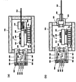
- the light source 100 is packaged in the form of a TO-CAN including an optical coupling lens 104 and is composed of a variable tunable filter 120 packaged in a single housing 511, Lt; / RTI >
- the light source 100 includes a photodiode 501 for monitoring a change in light output intensity, and is mounted on a sub-mount 502 having an L shape, The sub-mount 502 is positioned above the stem 504.
- a second temperature sensor including a thermoelectric cooler and a thermistor is provided below the stem 504 and the sub-mount 502 so that the optical gain of the light source 100 can be kept constant regardless of the external environment temperature
- a temperature regulator 503 is located.
- a lead-frame 505 for driving the light source 100 and the photodiode 501 or the temperature regulating device 503 is provided in the stem 504, and the light source 100, And is wire-bonded with the diode 501, the temperature regulator 503, and the like.
- the optical coupling lens 104 is provided with a window-glass 507 on the optical axis output from the light source 100 on a window of a cap 506 for hermitic-sealing, And are mounted together.
- the tunable filter 120 includes a thin film heater 108 including a metal thin film heating element and a first temperature sensor 112 (hereinafter, referred to as a " thin film heater ") including a Bragg grating formed on a substrate 105 having an optical waveguide. ).
- a thermostat device composed of a thermoelectric cooler 110 and a second temperature sensor 111 including a thermistor is attached to the inner bottom surface of the housing 511 and a heat insulating layer 109 is mounted on the thermoelectric cooler 110
- the semiconductor substrate 105 is mounted on the heat insulating layer 109.
- the surface of the thermoelectric cooler 110 attached to the inner bottom surface of the housing 511 is made of a metal material having a high thermal conductivity such as Al to increase the heat radiation efficiency by heating surface It is preferable to use a thermosetting resin having a high thermal conductivity when the thermoelectric cooler 110 is bonded.
- the housing 511 is preferably hermitic-sealed with a lead-frame (not shown) for driving the temperature regulating device, the heating element, and the temperature sensor on the side surface or the bottom surface .
- the single wavelength light oscillated in the resonator structure formed by the light source 100 and the tunable filter 120 is output through the optical fiber 113 and increases the optical coupling efficiency between the optical fiber 113 and the semiconductor optical waveguide 106 It is preferable to use a lens-shaped optical fiber 512 or a photo-coupling lens.
- the optical fiber support 509 including a V-groove is used to fix the lens-like optical fiber 512 as shown in FIG. 5A, .
- the lenticular optical fiber 113 and the support 509 are fixed by laser welding using a metal ferrule or by using a thermosetting or ultraviolet hardening resin and then by using an additional cover support 510 So that the bonding strength can be increased.
- the optical fiber 113 is fixed to the metal ferrule 514 so as to be spaced apart from the optical coupling lens 513 by the focal distance of the optical coupling lens 513 as shown in FIG. And is preferably fixed to the metal sleeve 515.
- the NA of the optical fiber 113 and the optical waveguide 106 side are similar to the NA values of the optical fiber 113 and the optical waveguide 106, It is preferable to prevent the AR coating having a reflectance of 1% or less from being formed and being reflected from the lens surface.
- the heat insulating layer 109 has a high temperature control according to the current applied to the heating element 108 for varying the wavelength when the thermal conductivity is large, but has a large power consumption because the heat dissipation efficiency through the thermoelectric cooler 110 is very large, On the contrary, when the thermal conductivity of the heat insulating layer 109 is small, the consumed electric power is reduced but the temperature control speed is slowed down.
- Fig. 6 shows a result of computer simulation of the relative temperature of the optical waveguide region according to the type of the insulating layer 109.
- the semiconductor substrate 105 is assumed to be a SOI substrate having a thickness of 100 m
- the thickness of the insulating layer 109 is assumed to be 50 ⁇ ⁇
- the insulating layer 109 used in the computer simulation is silicon, quartz or glass.
- Table 1 The heat capacity and thermal conductivity of the materials are summarized in Table 1 below.
- the heat insulating layer 109 of the present invention is characterized in that it has a small thermal conductivity and increases the thickness of the heat insulating layer 109 and reduces the contact area of the wavelength tunable filter with the semiconductor substrate, Minimize power consumption.
- a first temperature sensor 112 is provided on a semiconductor substrate 105 on which an optical waveguide is formed, and the optical waveguide formed by the thin film heater 108 is formed It is possible to monitor and control the temperature of the semiconductor substrate 105 in real time to reduce the wavelength stabilization time due to the temperature stabilization when the wavelength is varied.
- the wavelength tunable external resonant laser of the present invention may further comprise a controller.
- a controller When an optical transceiver employing the wavelength tunable external resonant laser of the present invention is operated on a WDM-PON optical link, The temperature control algorithm is shown in Fig.
- the current applied to the thermoelectric cooler 110 of the temperature controller is first adjusted by referring to the control value for each channel stored in the EPROM of the optical transceiver, 1 is compared with the resistance reference value of the channel-specific temperature sensor 112 stored in the EPROM through monitoring the resistance value of the temperature sensor 112 to control the application current of the thin film heater 108 so that the resistance value of the temperature sensor converges to the reference value .
- FIG. 8A and 8B illustrate another embodiment of the external resonant tunable laser module according to the present invention.
- the light source 100 and the tunable filter 120 are housed in the same housing 513, .
- the light source 100 is mounted on an L-shaped sub-mount 502 together with a photodiode 501 for monitoring a change in the intensity of oscillation light and a Cu Or a metal layer 512 of Al is placed on the upper surface of the thermoelectric cooler 110.
- the sub-mount is fixed to the metal layer 512 and mounted on the thermoelectric cooler 110 constituting the temperature control device.
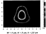
- the optical waveguides of the light source 100 and the tunable filter 120 are optically coupled through butt-coupling to form a resonator. At this time, the optical coupling efficiency varies depending on the distance between the exit surface of the light source 100 and the end face of the optical waveguide.
- the optical waveguide has a silicon lip waveguide structure, the width and height of the lap waveguide are 4 ⁇ m and 5 ⁇ m respectively, and the height of the slab waveguide is FIG. 9 shows a result of a computer simulation of the optical coupling efficiency according to the distance between the exit surface of the light source and the end surface of the optical waveguide in the case of 2.5 .mu.m.
- the maximum optical coupling efficiency is about 70% when the interval is 10 ⁇ m, and the tolerance range for 1dB loss is 2.5 ⁇ m and 3.5 ⁇ m for the horizontal and vertical directions, respectively.
- the maximum optical coupling efficiency is reduced to about 45%, which is about 40%, while the tolerable alignment error range for 1 dB loss is 6 ⁇ m or more for both horizontal and vertical directions.
- the optical coupling efficiency increases.
- the allowable range of alignment error decreases.
- the optical coupling efficiency decreases.
- a light distribution modulator (SSC) for reducing the spread angle of light emitted from the light source 100 Converters may be integrated in the light source 100. It is also preferable that the distance between the exit surface of the light source 100 and the incident surface of the optical waveguide is within 30 ⁇ ⁇ . It is preferable to use the lens-shaped optical fiber 512 or the optical coupling lens 513 as described in the embodiment of Figs. 5A and 5B.
Landscapes
- Physics & Mathematics (AREA)
- Electromagnetism (AREA)
- Optics & Photonics (AREA)
- Engineering & Computer Science (AREA)
- Plasma & Fusion (AREA)
- Condensed Matter Physics & Semiconductors (AREA)
- General Physics & Mathematics (AREA)
- Optical Couplings Of Light Guides (AREA)
- Optical Integrated Circuits (AREA)
Abstract
La présente invention concerne un module laser réglable pour cavité externe qui utilise l'effet thermo-optique d'un guide d'ondes optique semi-conducteur. Ledit module laser réglable de la présente invention comprend : une source lumineuse qui produit la lumière à large bande ; un guide d'ondes optique semi-conducteur dont une extrémité est optiquement couplée à la source lumineuse ; un réseau de Bragg qui est formé sur le guide d'ondes optique ; un élément thermique de film mince qui est positionné dans la partie supérieure du réseau de Bragg et effectue le réglage de la bande de réflexion du réseau de Bragg par l'effet thermo-optique ; un premier capteur thermique qui est positionné dans la partie supérieure du guide d'ondes optique ; un refroidisseur thermo-électrique (TEC) qui est disposé dans la partie inférieure du guide d'ondes optique ; une couche d'isolation thermique qui est prévue entre le guide d'ondes et le TEC ; et une fibre optique qui est optiquement couplée à l'autre extrémité du guide d'ondes optique.
Priority Applications (1)
| Application Number | Priority Date | Filing Date | Title |
|---|---|---|---|
| US13/377,733 US20120099611A1 (en) | 2009-06-12 | 2009-06-15 | External cavity tunable laser module |
Applications Claiming Priority (2)
| Application Number | Priority Date | Filing Date | Title |
|---|---|---|---|
| KR1020090052515A KR101038264B1 (ko) | 2009-06-12 | 2009-06-12 | 외부공진형 파장가변 레이저 모듈 |
| KR10-2009-0052515 | 2009-06-12 |
Publications (1)
| Publication Number | Publication Date |
|---|---|
| WO2010143763A1 true WO2010143763A1 (fr) | 2010-12-16 |
Family
ID=43309008
Family Applications (1)
| Application Number | Title | Priority Date | Filing Date |
|---|---|---|---|
| PCT/KR2009/003184 Ceased WO2010143763A1 (fr) | 2009-06-12 | 2009-06-15 | Module laser réglable pour cavité externe |
Country Status (3)
| Country | Link |
|---|---|
| US (1) | US20120099611A1 (fr) |
| KR (1) | KR101038264B1 (fr) |
| WO (1) | WO2010143763A1 (fr) |
Cited By (4)
| Publication number | Priority date | Publication date | Assignee | Title |
|---|---|---|---|---|
| CN105207056A (zh) * | 2014-05-30 | 2015-12-30 | 光速株式会社 | 具有折弯的光导波路的外部谐振器型激光器 |
| WO2016175595A1 (fr) * | 2015-04-29 | 2016-11-03 | (주)켐옵틱스 | Récepteur optique à longueur d'onde variable utilisant des réseaux de bragg de guides d'ondes |
| WO2017138649A1 (fr) * | 2016-02-12 | 2017-08-17 | 古河電気工業株式会社 | Module laser |
| KR101845269B1 (ko) | 2015-04-29 | 2018-04-04 | (주)켐옵틱스 | 도파로 브래그 격자를 사용한 파장 가변 광수신기 |
Families Citing this family (32)
| Publication number | Priority date | Publication date | Assignee | Title |
|---|---|---|---|---|
| KR101276338B1 (ko) * | 2009-12-18 | 2013-06-18 | 한국전자통신연구원 | 파장 가변 광원 |
| US20120257490A1 (en) * | 2011-04-07 | 2012-10-11 | Seagate Technology Llc | Gratings For Waveguide Coupling |
| CA2863983C (fr) | 2012-02-10 | 2022-05-10 | Nkt Photonics A/S | Dispositif laser avec module de commande et stabilisation de frequence |
| ES2657872T3 (es) * | 2012-06-21 | 2018-03-07 | Huawei Technologies Co., Ltd. | Filtro óptico sintonizable, conjunto óptico sintonizable y sistema de red óptica pasiva de múltiples longitudes de onda |
| US8831049B2 (en) | 2012-09-14 | 2014-09-09 | Laxense Inc. | Tunable optical system with hybrid integrated laser |
| US9477134B2 (en) * | 2012-12-28 | 2016-10-25 | Futurewei Technologies, Inc. | Hybrid integration using folded Mach-Zehnder modulator array block |
| US20140185980A1 (en) * | 2012-12-31 | 2014-07-03 | Futurewei Technologies, Inc. | Silicon-On-Insulator Platform for Integration of Tunable Laser Arrays |
| US9184564B2 (en) * | 2013-06-07 | 2015-11-10 | Ngk Insulators, Ltd. | External resonator type light emitting system |
| KR101631981B1 (ko) * | 2014-10-16 | 2016-06-20 | (주)켐옵틱스 | 메탈 온도센서 내장형 파장가변 필터 및 외부 공진기형 파장가변 레이저 모듈 |
| US9817190B2 (en) | 2013-10-24 | 2017-11-14 | Chemoptics Inc. | Tunable wavelength filter with embedded metal temperature sensor and its application to external-cavity type tunable wavelength laser |
| US20150116816A1 (en) * | 2013-10-31 | 2015-04-30 | Ipg Photonics Corporation | Compact Single Frequency Laser |
| US9331454B2 (en) | 2013-11-27 | 2016-05-03 | Ngk Insulators, Ltd. | External resonator type light emitting system |
| WO2015079939A1 (fr) * | 2013-11-27 | 2015-06-04 | 日本碍子株式会社 | Dispositif électroluminescent de type résonateur externe |
| JP5936777B2 (ja) * | 2013-11-27 | 2016-06-22 | 日本碍子株式会社 | グレーティング素子および外部共振器型発光装置 |
| CN104713487B (zh) * | 2013-12-11 | 2017-08-22 | 睿励科学仪器(上海)有限公司 | 可调节光源装置及包括该装置的精密测量设备 |
| FR3015135B1 (fr) * | 2013-12-13 | 2017-05-19 | Thales Sa | Source laser a largeur de raies reduite |
| JPWO2015108197A1 (ja) * | 2014-01-20 | 2017-03-23 | 日本碍子株式会社 | 外部共振器型発光装置 |
| JP6554035B2 (ja) * | 2014-05-01 | 2019-07-31 | 日本碍子株式会社 | グレーティング素子および外部共振器型発光装置 |
| WO2015178685A1 (fr) * | 2014-05-20 | 2015-11-26 | (주)켐옵틱스 | Module laser à longueur d'onde réglable à cavité externe pour emballage to-can |
| JP5641631B1 (ja) * | 2014-06-04 | 2014-12-17 | 日本碍子株式会社 | 外部共振器型発光装置 |
| US9368941B1 (en) | 2014-08-14 | 2016-06-14 | Google Inc. | Temperature compensation in an optical transmitter |
| US9933570B2 (en) * | 2016-03-01 | 2018-04-03 | Futurewei Technologies, Inc. | Integration of V-grooves on silicon-on-insulator (SOI) platform for direct fiber coupling |
| EP3550339B1 (fr) * | 2016-12-02 | 2024-07-24 | NGK Insulators, Ltd. | Élément optique et procédé de fabrication d'un élément optique |
| CN106684703B (zh) * | 2017-03-08 | 2019-12-31 | 成都优博创通信技术股份有限公司 | Twdm onu波长控制方法及其系统与关断深度控制电路 |
| US10732105B1 (en) * | 2019-02-15 | 2020-08-04 | Agilent Technologies, Inc. | Method and apparatus for characterizing laser gain chips |
| RU2717254C1 (ru) * | 2019-04-08 | 2020-03-19 | Федеральное государственное унитарное предприятие "Российский федеральный ядерный центр - Всероссийский научно-исследовательский институт технической физики имени академика Е.И. Забабахина" | Волоконный лазер для накачки активных элементов |
| CN110190509A (zh) * | 2019-05-24 | 2019-08-30 | 中国科学院半导体研究所 | 基于光子晶体激光器的波长稳定激光光源 |
| RU2748867C1 (ru) * | 2020-08-13 | 2021-06-01 | Федеральное государственное унитарное предприятие "Российский федеральный ядерный центр - Всероссийский научно-исследовательский институт технической физики имени академика Е.И. Забабахина" | Волоконный лазер для аддитивных технологий |
| CN117157845A (zh) * | 2021-03-24 | 2023-12-01 | 实光半导体科技(上海)有限公司 | 无模式跳变激光模块 |
| DE102022115317A1 (de) | 2022-06-20 | 2023-12-21 | Trumpf Laser Gmbh | Laservorrichtung |
| US12438340B2 (en) * | 2022-11-15 | 2025-10-07 | O-Net Communications, Inc. | Ultra small packaged tunable laser assembly |
| WO2024219805A1 (fr) * | 2023-04-17 | 2024-10-24 | 주식회사 포벨 | Laser de type résonateur externe ayant une largeur de ligne étroite |
Citations (3)
| Publication number | Priority date | Publication date | Assignee | Title |
|---|---|---|---|---|
| KR100413527B1 (ko) * | 2002-01-29 | 2004-01-03 | 한국전자통신연구원 | 단일 집적 반도체 광소자 제작방법 |
| KR20080052319A (ko) * | 2006-12-05 | 2008-06-11 | 한국전자통신연구원 | 평판형 광도파로(plc) 소자, 그 소자를 포함한 파장가변 광원 및 그 광원을 이용한 wdm-pon |
| KR20090011837A (ko) * | 2007-07-27 | 2009-02-02 | (주)켐옵틱스 | 폴리머 광 도파로형 파장가변 레이저 모듈 |
Family Cites Families (10)
| Publication number | Priority date | Publication date | Assignee | Title |
|---|---|---|---|---|
| JPH1197789A (ja) * | 1997-09-17 | 1999-04-09 | Fujitsu Ltd | 半導体レーザ装置 |
| GB2325334B (en) * | 1998-07-10 | 1999-04-14 | Bookham Technology Ltd | External cavity laser |
| CA2335529A1 (fr) * | 1999-04-20 | 2000-10-26 | Yuichiro Irie | Module a diode laser |
| JP2002176224A (ja) * | 2000-12-07 | 2002-06-21 | Fuji Photo Film Co Ltd | レーザー光源 |
| EP1468475A2 (fr) * | 2002-01-18 | 2004-10-20 | Oepic, Inc. | Boitiers to optoelectroniques a haute vitesse |
| US6989284B2 (en) * | 2002-05-31 | 2006-01-24 | Intel Corporation | Fabrication of a waveguide taper through ion implantation |
| US6917636B2 (en) * | 2002-08-22 | 2005-07-12 | Xponent Photonics Inc | Grating-stabilized semiconductor laser |
| CA2453760A1 (fr) * | 2002-12-20 | 2004-06-20 | Spectalis Corp. | Lasers a cavite externe |
| KR20050045145A (ko) * | 2003-11-10 | 2005-05-17 | 삼성전자주식회사 | 반도체 광패키지 |
| KR100637928B1 (ko) * | 2004-10-13 | 2006-10-24 | 한국전자통신연구원 | 파장 가변 광송신 모듈 |
-
2009
- 2009-06-12 KR KR1020090052515A patent/KR101038264B1/ko active Active
- 2009-06-15 WO PCT/KR2009/003184 patent/WO2010143763A1/fr not_active Ceased
- 2009-06-15 US US13/377,733 patent/US20120099611A1/en not_active Abandoned
Patent Citations (3)
| Publication number | Priority date | Publication date | Assignee | Title |
|---|---|---|---|---|
| KR100413527B1 (ko) * | 2002-01-29 | 2004-01-03 | 한국전자통신연구원 | 단일 집적 반도체 광소자 제작방법 |
| KR20080052319A (ko) * | 2006-12-05 | 2008-06-11 | 한국전자통신연구원 | 평판형 광도파로(plc) 소자, 그 소자를 포함한 파장가변 광원 및 그 광원을 이용한 wdm-pon |
| KR20090011837A (ko) * | 2007-07-27 | 2009-02-02 | (주)켐옵틱스 | 폴리머 광 도파로형 파장가변 레이저 모듈 |
Cited By (7)
| Publication number | Priority date | Publication date | Assignee | Title |
|---|---|---|---|---|
| CN105207056A (zh) * | 2014-05-30 | 2015-12-30 | 光速株式会社 | 具有折弯的光导波路的外部谐振器型激光器 |
| WO2016175595A1 (fr) * | 2015-04-29 | 2016-11-03 | (주)켐옵틱스 | Récepteur optique à longueur d'onde variable utilisant des réseaux de bragg de guides d'ondes |
| KR101845269B1 (ko) | 2015-04-29 | 2018-04-04 | (주)켐옵틱스 | 도파로 브래그 격자를 사용한 파장 가변 광수신기 |
| WO2017138649A1 (fr) * | 2016-02-12 | 2017-08-17 | 古河電気工業株式会社 | Module laser |
| US20180342850A1 (en) * | 2016-02-12 | 2018-11-29 | Furukawa Electric Co., Ltd. | Laser module |
| JPWO2017138649A1 (ja) * | 2016-02-12 | 2018-12-13 | 古河電気工業株式会社 | レーザモジュール |
| US10811840B2 (en) | 2016-02-12 | 2020-10-20 | Furukawa Electric Co., Ltd. | Laser module |
Also Published As
| Publication number | Publication date |
|---|---|
| KR101038264B1 (ko) | 2011-06-01 |
| KR20100133797A (ko) | 2010-12-22 |
| US20120099611A1 (en) | 2012-04-26 |
Similar Documents
| Publication | Publication Date | Title |
|---|---|---|
| WO2010143763A1 (fr) | Module laser réglable pour cavité externe | |
| KR100772529B1 (ko) | 파장 가변 외부 공진 레이저 | |
| US8615025B2 (en) | Method and system for hybrid integration of a tunable laser | |
| US8559470B2 (en) | Method and system for hybrid integration of a tunable laser and a phase modulator | |
| US8605766B2 (en) | Method and system for hybrid integration of a tunable laser and a mach zehnder modulator | |
| US8867578B2 (en) | Method and system for hybrid integration of a tunable laser for a cable TV transmitter | |
| US8831049B2 (en) | Tunable optical system with hybrid integrated laser | |
| US7440643B2 (en) | Variable light controlling device and variable light controlling method | |
| US9318868B2 (en) | Tunable hybrid laser with carrier-induced phase control | |
| KR101461158B1 (ko) | 파장 가변 외부 공진 레이저 모듈 | |
| KR101276338B1 (ko) | 파장 가변 광원 | |
| CN1309827A (zh) | 外腔激光器 | |
| KR100637928B1 (ko) | 파장 가변 광송신 모듈 | |
| KR100842297B1 (ko) | 온도 무의존성 외부공진레이저 | |
| KR100420950B1 (ko) | 파장 가변 레이저 광원 | |
| JP5515447B2 (ja) | 導波路型波長ロッカー及び光モジュールの製造方法 | |
| Takeuchi et al. | Wavelength tunable laser with silica-waveguide ring resonators | |
| KR20150047699A (ko) | 고효율 외부 공진기형 파장가변 레이저 | |
| KR100493089B1 (ko) | 집적광학장치 | |
| WO2025027739A1 (fr) | Convertisseur de taille de point et dispositif intégré optique | |
| WO2007123334A1 (fr) | Laser à cavité externe réglable en longueur d'onde | |
| EP1024564A2 (fr) | Système de transmission optique et émetteur optique | |
| JP2000277845A (ja) | 発光モジュール | |
| KR20110103217A (ko) | 파장 가변 광원 |
Legal Events
| Date | Code | Title | Description |
|---|---|---|---|
| 121 | Ep: the epo has been informed by wipo that ep was designated in this application |
Ref document number: 09845857 Country of ref document: EP Kind code of ref document: A1 |
|
| NENP | Non-entry into the national phase |
Ref country code: DE |
|
| WWE | Wipo information: entry into national phase |
Ref document number: 13377733 Country of ref document: US |
|
| 122 | Ep: pct application non-entry in european phase |
Ref document number: 09845857 Country of ref document: EP Kind code of ref document: A1 |