WO2010143881A2 - Structure de banc d'une carte fpga destinée à la vérification de semiconducteurs - Google Patents
Structure de banc d'une carte fpga destinée à la vérification de semiconducteurs Download PDFInfo
- Publication number
- WO2010143881A2 WO2010143881A2 PCT/KR2010/003692 KR2010003692W WO2010143881A2 WO 2010143881 A2 WO2010143881 A2 WO 2010143881A2 KR 2010003692 W KR2010003692 W KR 2010003692W WO 2010143881 A2 WO2010143881 A2 WO 2010143881A2
- Authority
- WO
- WIPO (PCT)
- Prior art keywords
- fpga
- board
- connector
- allocated
- semiconductor
- Prior art date
- Legal status (The legal status is an assumption and is not a legal conclusion. Google has not performed a legal analysis and makes no representation as to the accuracy of the status listed.)
- Ceased
Links
Images




Classifications
-
- G—PHYSICS
- G01—MEASURING; TESTING
- G01R—MEASURING ELECTRIC VARIABLES; MEASURING MAGNETIC VARIABLES
- G01R31/00—Arrangements for testing electric properties; Arrangements for locating electric faults; Arrangements for electrical testing characterised by what is being tested not provided for elsewhere
- G01R31/28—Testing of electronic circuits, e.g. by signal tracer
- G01R31/317—Testing of digital circuits
- G01R31/3181—Functional testing
- G01R31/3185—Reconfiguring for testing, e.g. LSSD, partitioning
- G01R31/318516—Test of programmable logic devices [PLDs]
- G01R31/318519—Test of field programmable gate arrays [FPGA]
Definitions
- the present invention relates to a bank structure of a semiconductor verification FPGA board, and more particularly, to a bank structure of a semiconductor verification FPGA board for more effectively arranging a connection between an input / output pin of an FPGA device and a board. will be.
- FPGA component devices are used to validate large designs.
- Field programmable arrays are semiconductor devices that include programmable logic elements and programmable internals. Programmable logic PPC elements can be programmed by duplicating basic logic gate functions such as AND, OR, XOR, NOT, and more complex decoder or computational functions. Most FPGAs also include a simple flip-flop or memory element in more complete memory blocks in programmable logic elements (also called logic blocks in FPGAs).
- PLDs programmable logic devices
- PCB boards configured for semiconductor design verification must be disassembled to recycle expensive FPGA devices after the verification work is completed for the purpose, but FPGAs with high-capacity logic circuits are highly integrated package parts with more than 1,000 pins. .
- the PCB board of the system for semiconductor design verification is manufactured by placing and wiring in a 2D plane by using a large number of highly integrated FPGA devices with more than 1,000 input / output pins.
- the wiring between the FPGA devices becomes very long.
- An object of the present invention to solve the above problems is to provide an effective mounting structure for connecting the dense input / output pins of the FPGA device to the board.
- the present invention provides a programmable logic device (PLD) board for verifying a semiconductor design, comprising: an FPGA device having a logic circuit for verifying a semiconductor and a plurality of input / output signals therefor At least one FPGA board equipped with a connector and a plurality of input / output pins configured in the FPGA device are divided into any number and assigned to a plurality of areas, respectively, and connectors provided in the FPGA board corresponding to each allocated area. In addition, it is assigned to a plurality of areas, characterized in that configured to integrate the input / output pin assignment area of the FPGA device and the area assigned to the connector correspondingly.
- PLD programmable logic device
- the connector may be allocated according to the input / output pins of the FPGA device, and the spare area may be allocated.
- the allocation region to the FPGA device characterized in that the allocation to 40 pin, 20 pin, 10 pin, respectively.
- Each connector may be allocated to six areas and one area to a spare area.
- the FPGA device is characterized in that the allocation to 38 areas.
- the apparatus may further include a switching board having a switching element for selectively blocking signals between the plurality of FPGA boards stacked through the connector, and having a same connector as the connector and connected between the FPGA boards. It features.
- the present invention configured and operated as described above can be effectively configured by minimizing patterning wiring by dividing into arbitrary sections of an area of an input / output pin and minimizing a distance between connectors connected thereto and assigning the connector according to an arbitrary area. There is an advantage to that.
- FIG. 1 is a schematic perspective view of an FPGA board for semiconductor verification according to the present invention
- Figure 2 is a plan view showing the FPGA device input / output pin section of the FPGA board according to the present invention
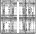
- FIG. 3 is a diagram illustrating an input / output pin assignment of an FPGA board allocated to connector 1 according to an embodiment of the present invention
- FIG. 4 is a perspective view showing a switching board used in the FPGA board for semiconductor verification according to the present invention.
- FIG. 5 is a schematic cross-sectional view showing a stacked form of an FPGA board and a switching board according to the present invention.
- FIG. 1 is a schematic perspective view of an FPGA board for semiconductor verification according to the present invention
- Figure 2 is a plan view showing the FPGA device input / output pin section of the FPGA board according to the present invention
- Figure 3 is an embodiment according to the present invention 1
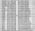
- Figure 4 shows the input and output pins assigned to the FPGA board assigned to the connector No. 4
- Figure 5 is a FPGA board and the switching board according to the present invention It is a schematic sectional drawing which shows the lamination form of the.
- the present invention provides a programmable logic device (PLD) board for verifying a semiconductor design, the FPGA device 110 having a logic circuit for verifying a semiconductor and a plurality of connectors 200 for inputting / outputting signals thereto.
- PLD programmable logic device
- At least one FPGA board 100 and a plurality of input / output pins configured in the FPGA device is divided into a plurality of areas, each of which is assigned to a plurality of areas, each corresponding to the allocated area provided on the FPGA board
- the connector may be allocated to a plurality of areas, and the input / output pin assignment area of the FPGA device and the area allocated to the connector may be mounted correspondingly.
- the FPGA board 100 is a high-density FPGA device is mounted on the PCB, and after writing a program designed to verify the semiconductor design on the FPGA device 110 to check the operation of the semiconductor design. At this time, a plurality of FPGA boards are used as the capacity of the logical circuit required for operation verification is increased.
- one FPGA device is mounted on each FPGA board, and a plurality of connectors 200 having a common standard are provided. Signal processing is performed between boards by connecting FPGA boards through connectors.
- the connector 120 is to secure the connectivity of the FPGA board, the connection pin of the connector is electrically connected to the input / output pins of the FPGA device (110).
- the connector 120 is connected to a plurality of connectors in a mutually corresponding form as a connector structure capable of being connected up / down.
- a connector structure capable of being connected up / down.
- signal input / output of 1440 pins can be secured.
- the FPGA board includes a power supply unit (unsigned) for receiving power and a plurality of component elements for input / output signal processing, and a code setting unit for identifying a code (ID) according to each FPGA board ( Unsigned) is configured in a switch system.
- the input / output pins of the FPGA device are allocated to a plurality of areas.
- the key technical point is to be able to effectively mount the signal connection between the pin and the connector.
- the input / output pins of the FPGA device are divided into arbitrary numbers and allocated to a plurality of areas.
- an FPGA device having an input / output pin of 1200 pins will be described.
- a plurality of areas are divided into a total of 38 areas by assigning numbers having # 01 to # 08 and # 11 to # 34, and the number of pins in each area is 10 pins or 20. Divide the pins into 40 pins. This is only a configuration according to an embodiment mentioned in the present invention, it is possible to change the pin count and the allocation area according to the FPGA device.
- Each partitioned area is mounted on the FPGA board plane so as to be connected to the closest one between the FPGA device and the connector, and the connector 200 is also allocated to an arbitrary area.
- FIG. 3 shows the allocation number between each pin and the number 1 connector of the FPGA element.
- the FPGA board according to the present invention has eight connectors and is assigned to the connectors for each area allocated to the device.
- the number of allocation pins for each region of the FPGA device is divided into 10, 20, and 40.
- the number of pins of the device does not correspond to the number of pins of the connector. Assign it to an area.
- 40 pins of the region corresponding to # 28 are allocated to both pins 10 and 30 on both sides of the region of # 28 assigned to connector 1.
- the connector is formed by 30 pins on both sides, one side allocates all 30 pins and the other 10 pins are allocated, so the remaining 20 pins allocate area # 20 of the FPGA device. The remaining pins in area # 20 are then reassigned to the next connector.
- the FPGA device can be distinguished by assigning each region and a connector installed close to each area, and the wiring length between the device and the connector can be minimized, which is effective in patterning.
- the connector secures an arbitrary number of pins as a spare area without allocating the FPGA element 110 pin. This is secured for each connector.
- the spare area may not be secured according to the type of the FPGA device, and may also vary according to the specification of the connector.
- an FPGA device 110 having a high-density logic circuit for semiconductor design verification is mounted on a board, and two FPGA boards 100 are stacked to connect a signal to the connector 200 and the FPGA.
- Device input / output pin connections are mounted on the PCB board by allocating multiple areas. By stacking two or more FPGA boards configured in this way, signals can be connected flexibly.
- a separate switching board is applied to selectively connect signals between the boards.
- the switching board 300 is a board for switching signals when a plurality of FPGA boards are combined, and a connector 200 having the same standard as the connector 120 configured in the FPGA board is provided.
- the switching board 300 is provided with a plurality of switching elements 310 so that the switching board 300 can be automatically controlled through a manual switching or control by a user.
- the present invention is implemented by applying a dip switch device for a passive implementation as an example, but is not limited thereto.
- the switching device may be provided to correspond to the eight connectors 200 provided on the switching board, like the FPGA board, to block signals transmitted through the respective connectors.
- the connector 200 is different from the connector 120 provided in the FPGA board, in the case of the switching board, the pins provided at the upper and lower ends of the connector are configured to be connected via a switching element.
- the upper and lower pins have a directly connected structure.
- the switching device can block partial signals of the FPGA device as needed, thereby flexibly controlling the inter-board signal flow.
- the present invention configured as described above can manufacture a wiring length very effectively between an FPGA element having a dense input / output pin and a connector connected thereto, and has an advantage of ensuring identification due to matching between any designated allocation area.
Landscapes
- Engineering & Computer Science (AREA)
- General Engineering & Computer Science (AREA)
- Physics & Mathematics (AREA)
- General Physics & Mathematics (AREA)
- Design And Manufacture Of Integrated Circuits (AREA)
- Computer Hardware Design (AREA)
- Microelectronics & Electronic Packaging (AREA)
- Tests Of Electronic Circuits (AREA)
Abstract
L’invention concerne une structure de banc d'une carte FPGA (matrice prédiffusée programmable par l'utilisateur) destinée à la vérification de semiconducteurs. Une carte à dispositif logique programmable (PLD) destinée à la vérification de semiconducteurs comprend: au moins une carte FPGA dotée d'un dispositif FPGA présentant un circuit logique de vérification de semiconducteurs, et de plusieurs connecteurs pour entrer un signal dans le dispositif FPGA ou sortir un signal dudit dispositif. Plusieurs broches d'entrée-sortie du dispositif FPGA sont divisées en un nombre arbitraire de groupes, chaque groupe étant attribué à un emplacement. Les connecteurs de la carte FPGA sont également attribués à plusieurs emplacements correspondant aux emplacements respectifs attribués aux broches d'entrée-sortie. Les emplacements attribués aux broches d'entrée-sortie du dispositif FPGA correspondent et sont intégrées aux emplacements attribués aux connecteurs. La carte FPGA ainsi configurée optimise la connectivité entre le dispositif FPGA et les connecteurs.
Applications Claiming Priority (2)
| Application Number | Priority Date | Filing Date | Title |
|---|---|---|---|
| KR20090052439A KR101090303B1 (ko) | 2009-06-12 | 2009-06-12 | 반도체 검증용 fpga 보드의 뱅크구조 |
| KR10-2009-0052439 | 2009-06-12 |
Publications (2)
| Publication Number | Publication Date |
|---|---|
| WO2010143881A2 true WO2010143881A2 (fr) | 2010-12-16 |
| WO2010143881A3 WO2010143881A3 (fr) | 2011-03-31 |
Family
ID=43309362
Family Applications (1)
| Application Number | Title | Priority Date | Filing Date |
|---|---|---|---|
| PCT/KR2010/003692 Ceased WO2010143881A2 (fr) | 2009-06-12 | 2010-06-09 | Structure de banc d'une carte fpga destinée à la vérification de semiconducteurs |
Country Status (2)
| Country | Link |
|---|---|
| KR (1) | KR101090303B1 (fr) |
| WO (1) | WO2010143881A2 (fr) |
Family Cites Families (7)
| Publication number | Priority date | Publication date | Assignee | Title |
|---|---|---|---|---|
| WO1993012638A1 (fr) | 1991-12-18 | 1993-06-24 | Crosspoint Solutions, Inc. | Architecture etendue pour reseaux de portes programmables par l'utilisateur |
| JP3020030B2 (ja) * | 1998-04-01 | 2000-03-15 | モレックス インコーポレーテッド | バーンインソケット |
| US20060117274A1 (en) * | 1998-08-31 | 2006-06-01 | Tseng Ping-Sheng | Behavior processor system and method |
| KR20000013186U (ko) * | 1998-12-23 | 2000-07-15 | 서평원 | 보드 계측용 테스트 보드 |
| JP2001318124A (ja) | 2000-05-09 | 2001-11-16 | Hitachi Ltd | 論理モジュール |
| KR100420112B1 (ko) * | 2001-06-15 | 2004-03-02 | 주식회사 마이다스엔지니어링 | 라이터 일체형 씨피엘디 에프피지에이 보드 |
| JP2006079447A (ja) | 2004-09-10 | 2006-03-23 | Fujitsu Ltd | 集積回路設計支援装置、集積回路設計支援方法及び集積回路設計支援プログラム |
-
2009
- 2009-06-12 KR KR20090052439A patent/KR101090303B1/ko not_active Expired - Fee Related
-
2010
- 2010-06-09 WO PCT/KR2010/003692 patent/WO2010143881A2/fr not_active Ceased
Also Published As
| Publication number | Publication date |
|---|---|
| KR20100133741A (ko) | 2010-12-22 |
| WO2010143881A3 (fr) | 2011-03-31 |
| KR101090303B1 (ko) | 2011-12-07 |
Similar Documents
| Publication | Publication Date | Title |
|---|---|---|
| US5887158A (en) | Switching midplane and interconnecting system for interconnecting large numbers of signals | |
| US8107466B2 (en) | Flexible network switch fabric for clustering system | |
| US20170052919A1 (en) | Backplane interface sets | |
| US20090271556A1 (en) | Connecting multiple peripheral interfaces into one attachment point | |
| JPH02281359A (ja) | 放射型・パラレル・システムバス | |
| US10010007B2 (en) | Multi-slot plug-in card | |
| HUT69838A (en) | Cable management system with automating mapping | |
| US5982634A (en) | High speed switch package provides reduced path lengths for electrical paths through the package | |
| EP2558896B1 (fr) | Systeme comprenant plusieurs dispositifs de distribution | |
| CN102053650B (zh) | 背板系统及背板信号线布线方法 | |
| JP3660552B2 (ja) | 相互接続システム | |
| KR20060111505A (ko) | 멀티프로세서 시스템들에서 사용하기 위한 프로세서써로게이트와 이를 사용하는 멀티프로세서 시스템 | |
| CN103809698A (zh) | 记忆体组合及应用其的电脑系统 | |
| US8570764B2 (en) | Backplane and backplane communication system | |
| US6578103B1 (en) | Compact PCI backplane and method of data transfer across the compact PCI backplane | |
| US6855001B2 (en) | Modular system | |
| US7800915B2 (en) | Printed board assembly | |
| US6286093B1 (en) | Multi-bus programmable interconnect architecture | |
| WO2010143876A2 (fr) | Carte fpga superposée destinée à la vérification de semiconducteurs | |
| CN114079211B (zh) | 通信设备 | |
| KR101090303B1 (ko) | 반도체 검증용 fpga 보드의 뱅크구조 | |
| US7100130B2 (en) | Device for the emulation of designs for integrated circuits | |
| CN118555741A (zh) | 电路板和电子设备 | |
| US20040210700A1 (en) | Compact PCI backplane and method of data transfer across the compact PCI backplane | |
| CA1101971A (fr) | Systeme de controle pour lignes telephoniques interurbaines |
Legal Events
| Date | Code | Title | Description |
|---|---|---|---|
| 121 | Ep: the epo has been informed by wipo that ep was designated in this application |
Ref document number: 10786364 Country of ref document: EP Kind code of ref document: A2 |
|
| NENP | Non-entry into the national phase |
Ref country code: DE |
|
| 122 | Ep: pct application non-entry in european phase |
Ref document number: 10786364 Country of ref document: EP Kind code of ref document: A2 |