WO2010146655A1 - 記録ヘッド及び記録ヘッドの検査装置 - Google Patents
記録ヘッド及び記録ヘッドの検査装置 Download PDFInfo
- Publication number
- WO2010146655A1 WO2010146655A1 PCT/JP2009/060910 JP2009060910W WO2010146655A1 WO 2010146655 A1 WO2010146655 A1 WO 2010146655A1 JP 2009060910 W JP2009060910 W JP 2009060910W WO 2010146655 A1 WO2010146655 A1 WO 2010146655A1
- Authority
- WO
- WIPO (PCT)
- Prior art keywords
- signal
- recording
- temperature
- circuit
- signal generation
- Prior art date
- Legal status (The legal status is an assumption and is not a legal conclusion. Google has not performed a legal analysis and makes no representation as to the accuracy of the status listed.)
- Ceased
Links
Images




Classifications
-
- B—PERFORMING OPERATIONS; TRANSPORTING
- B41—PRINTING; LINING MACHINES; TYPEWRITERS; STAMPS
- B41J—TYPEWRITERS; SELECTIVE PRINTING MECHANISMS, i.e. MECHANISMS PRINTING OTHERWISE THAN FROM A FORME; CORRECTION OF TYPOGRAPHICAL ERRORS
- B41J2/00—Typewriters or selective printing mechanisms characterised by the printing or marking process for which they are designed
- B41J2/005—Typewriters or selective printing mechanisms characterised by the printing or marking process for which they are designed characterised by bringing liquid or particles selectively into contact with a printing material
- B41J2/01—Ink jet
- B41J2/015—Ink jet characterised by the jet generation process
- B41J2/04—Ink jet characterised by the jet generation process generating single droplets or particles on demand
- B41J2/045—Ink jet characterised by the jet generation process generating single droplets or particles on demand by pressure, e.g. electromechanical transducers
- B41J2/04501—Control methods or devices therefor, e.g. driver circuits, control circuits
- B41J2/0458—Control methods or devices therefor, e.g. driver circuits, control circuits controlling heads based on heating elements forming bubbles
-
- B—PERFORMING OPERATIONS; TRANSPORTING
- B41—PRINTING; LINING MACHINES; TYPEWRITERS; STAMPS
- B41J—TYPEWRITERS; SELECTIVE PRINTING MECHANISMS, i.e. MECHANISMS PRINTING OTHERWISE THAN FROM A FORME; CORRECTION OF TYPOGRAPHICAL ERRORS
- B41J2/00—Typewriters or selective printing mechanisms characterised by the printing or marking process for which they are designed
- B41J2/005—Typewriters or selective printing mechanisms characterised by the printing or marking process for which they are designed characterised by bringing liquid or particles selectively into contact with a printing material
- B41J2/01—Ink jet
- B41J2/015—Ink jet characterised by the jet generation process
- B41J2/04—Ink jet characterised by the jet generation process generating single droplets or particles on demand
- B41J2/045—Ink jet characterised by the jet generation process generating single droplets or particles on demand by pressure, e.g. electromechanical transducers
- B41J2/04501—Control methods or devices therefor, e.g. driver circuits, control circuits
- B41J2/04541—Specific driving circuit
-
- B—PERFORMING OPERATIONS; TRANSPORTING
- B41—PRINTING; LINING MACHINES; TYPEWRITERS; STAMPS
- B41J—TYPEWRITERS; SELECTIVE PRINTING MECHANISMS, i.e. MECHANISMS PRINTING OTHERWISE THAN FROM A FORME; CORRECTION OF TYPOGRAPHICAL ERRORS
- B41J2/00—Typewriters or selective printing mechanisms characterised by the printing or marking process for which they are designed
- B41J2/005—Typewriters or selective printing mechanisms characterised by the printing or marking process for which they are designed characterised by bringing liquid or particles selectively into contact with a printing material
- B41J2/01—Ink jet
- B41J2/015—Ink jet characterised by the jet generation process
- B41J2/04—Ink jet characterised by the jet generation process generating single droplets or particles on demand
- B41J2/045—Ink jet characterised by the jet generation process generating single droplets or particles on demand by pressure, e.g. electromechanical transducers
- B41J2/04501—Control methods or devices therefor, e.g. driver circuits, control circuits
- B41J2/04543—Block driving
-
- B—PERFORMING OPERATIONS; TRANSPORTING
- B41—PRINTING; LINING MACHINES; TYPEWRITERS; STAMPS
- B41J—TYPEWRITERS; SELECTIVE PRINTING MECHANISMS, i.e. MECHANISMS PRINTING OTHERWISE THAN FROM A FORME; CORRECTION OF TYPOGRAPHICAL ERRORS
- B41J2/00—Typewriters or selective printing mechanisms characterised by the printing or marking process for which they are designed
- B41J2/005—Typewriters or selective printing mechanisms characterised by the printing or marking process for which they are designed characterised by bringing liquid or particles selectively into contact with a printing material
- B41J2/01—Ink jet
- B41J2/015—Ink jet characterised by the jet generation process
- B41J2/04—Ink jet characterised by the jet generation process generating single droplets or particles on demand
- B41J2/045—Ink jet characterised by the jet generation process generating single droplets or particles on demand by pressure, e.g. electromechanical transducers
- B41J2/04501—Control methods or devices therefor, e.g. driver circuits, control circuits
- B41J2/04563—Control methods or devices therefor, e.g. driver circuits, control circuits detecting head temperature; Ink temperature
-
- B—PERFORMING OPERATIONS; TRANSPORTING
- B41—PRINTING; LINING MACHINES; TYPEWRITERS; STAMPS
- B41J—TYPEWRITERS; SELECTIVE PRINTING MECHANISMS, i.e. MECHANISMS PRINTING OTHERWISE THAN FROM A FORME; CORRECTION OF TYPOGRAPHICAL ERRORS
- B41J2/00—Typewriters or selective printing mechanisms characterised by the printing or marking process for which they are designed
- B41J2/005—Typewriters or selective printing mechanisms characterised by the printing or marking process for which they are designed characterised by bringing liquid or particles selectively into contact with a printing material
- B41J2/01—Ink jet
- B41J2/135—Nozzles
- B41J2/14—Structure thereof only for on-demand ink jet heads
- B41J2/14016—Structure of bubble jet print heads
- B41J2/14088—Structure of heating means
- B41J2/14112—Resistive element
- B41J2/14129—Layer structure
-
- B—PERFORMING OPERATIONS; TRANSPORTING
- B41—PRINTING; LINING MACHINES; TYPEWRITERS; STAMPS
- B41J—TYPEWRITERS; SELECTIVE PRINTING MECHANISMS, i.e. MECHANISMS PRINTING OTHERWISE THAN FROM A FORME; CORRECTION OF TYPOGRAPHICAL ERRORS
- B41J2/00—Typewriters or selective printing mechanisms characterised by the printing or marking process for which they are designed
- B41J2/005—Typewriters or selective printing mechanisms characterised by the printing or marking process for which they are designed characterised by bringing liquid or particles selectively into contact with a printing material
- B41J2/01—Ink jet
- B41J2/135—Nozzles
- B41J2/14—Structure thereof only for on-demand ink jet heads
- B41J2002/14354—Sensor in each pressure chamber
Definitions
- the present invention relates to a recording head and a recording head inspection apparatus.
- Cited Document 1 describes a configuration in which a drive circuit for driving a heater and a temperature detection circuit for acquiring temperature information from a temperature sensor are provided and controlled by a signal from a control unit in the recording apparatus main body.
- Cited Document 2 describes a configuration in which a heater drive circuit and a temperature detection circuit are controlled using a common signal.
- the recording head of the present invention is a recording head in which first, second, and third recording elements are arranged in order, and is provided corresponding to each of the first, second, and third recording elements.
- a signal generation circuit that generates a signal for sequentially driving the first, second, and third recording elements, and the temperature acquisition circuit corresponding to the first recording element includes the second recording element. Temperature acquisition is performed based on a signal generated by a drive circuit corresponding to the element and a signal generated by a drive circuit corresponding to the third recording element.
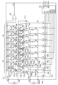
- FIG. 2 is a block diagram of a recording element substrate in the first embodiment.
- FIG. 3 is a block diagram of a signal generation unit 102.
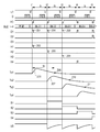
- FIG. FIG. 4 is a diagram for explaining control timing of a printing element substrate in the first embodiment. It is a perspective view of a recording head.
- FIG. 6 is a block diagram of a recording element substrate in a second embodiment.
- FIG. 9 is a diagram for explaining control timing of a recording element substrate in a second embodiment.
- FIG. 9 is a diagram for explaining control timing of a recording element substrate in a second embodiment. It is a figure explaining the relationship between the temperature measured with the temperature detection element, and the discharge state. It is a processing flow of the signal generation part of the test
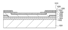
- FIG. 3 is a diagram illustrating a cross section of a recording element substrate.
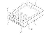
- FIG. 3 is a perspective view of the recording head 1.
- the recording head 1 ejects ink in the liquid path 6 from the ejection port 3 using the thermal energy of the recording element 2.
- Ink is supplied from the common liquid chamber 5 to the liquid path 6.
- the recording element 2 is provided on the substrate 4.
- FIG. 6 shows temperature profiles detected by the temperature detection element (temperature sensor) before and after the drive timing of the recording element (heater).
- the vertical axis is temperature
- the horizontal axis is time.
- the timing t62 is the timing when the heater driving is started
- the timing t63 is the timing when the heater driving is finished.
- Line (a) is a temperature profile when ink is ejected normally.
- a dotted line (b) is a temperature profile in the case of ejection failure caused by bubbles remaining in the nozzle.
- a dotted line (c) is a temperature profile in the case of ejection failure that occurs because impurities are accumulated in the ink flow path and ink refilling is not performed normally.
- a dotted line (d) is a temperature profile in the case of ejection failure caused by ink adhering to the nozzle surface.
- a dotted line (e) is a temperature profile in the case of a discharge failure caused by a foreign matter clogged in the discharge port. As described above, the ink ejection state and the temperature profile correspond to each other.
- an inflection point appears at t66 after about 4.2 ⁇ sec from t63 when the temperature reaches the maximum temperature T3.
- the timing at which this inflection point occurs is between timing t64 and timing t65.
- the timing at which the inflection point appears is determined by the structure and characteristics such as the ejection port of the recording head, the ink flow path, and the heat generation capability of the heater.
- the inflection point does not appear or the timing at which the inflection point appears is different from the timing at which the inflection point appears. Accordingly, if the temperature information from timing t64 to timing t65 is acquired with reference to the timing at which the maximum temperature is reached or the timing at which the heater is started, the ink ejection state can be determined.
- the method for determining the ink discharge state is a method using the initial temperature T1 before the ink temperature starts to rise (for example, timing t61), the temperature T4 before the inflection point, or the temperature T5 after the inflection point. There is. For this purpose, for example, temperature information from timing t61 to t64 is acquired.
- FIG. 8 is a diagram for explaining the control configuration of the inspection apparatus 801.
- the signal generation unit 127 In response to an instruction from the operation unit 132, the signal generation unit 127 outputs a clock signal (CLK), a data signal (D), a latch signal (LT), and a heat enable signal (HE) to the printing element substrate 101.
- the AD converter 128 receives the analog signal VS from the recording element substrate 101 and converts it into a digital signal.
- the AD converter 128 outputs a digital signal to the buffer 129.
- the computing unit 130 computes the second derivative of the signal read from the buffer memory 129.
- the determination unit 131 determines the calculation result of the calculator 130.
- the signal generation unit 127 displays the determination result held by the determination unit 131 on a display unit provided in the operation unit 132.
- signals output from the signal generation unit 127 to other blocks such as the AD converter 128, the arithmetic unit 130, and the determination unit 131 are omitted.
- the signal generation unit 127 outputs a signal synchronized with a heat enable signal (HE), a latch signal (LT), or the like, and controls operations of the AD converter 128, the arithmetic unit 130, and the determination unit 131.
- HE heat enable signal
- LT latch signal
- the recording element substrate 101 includes a silicon substrate 1001, a field oxide film 1002 such as SiO2, an insulating film 1003, a temperature detection element 1005 formed of a thin film resistor, a wiring 1004 connecting the temperature detection element 1005, and an interlayer insulation such as SiO.
- the recording element substrate 101 is formed by a semiconductor process.
- the recording element substrate 101 includes a plurality of temperature detection elements 1005 and a plurality of recording elements 1007.
- FIG. 1A is a diagram illustrating the configuration of the recording element substrate 101 according to the first embodiment.
- the recording element substrate 101 corresponds to the substrate 4 in FIG.
- This circuit configuration is a circuit configuration for acquiring temperature information from timing t64 to timing t65 described in FIG.
- the recording element substrate 101 includes eight recording elements (heaters) and eight temperature detection elements (temperature sensors), respectively, in the order shown in FIG. Arranged.
- the recording element substrate 101 includes a voltage source 113 for the recording element, a constant current source 125 for the temperature detection element, and an input unit (pad or terminal) for inputting signals and information from the outside.
- the switch element (MOS transistor) 106a controls the application of the voltage of the voltage source 113 to the recording element (heater) 107a.
- the switch elements 117a, 119a, and 120a control the application of the current of the constant current source 125 to the temperature detection element (temperature sensor) 118a.
- the temperature detection element (temperature sensor) 118a measures the temperature of the recording element (heater) 107a.
- the signal generation circuit 102 inputs the clock signal (CLK), the data signal (D), the latch signal (LT), and the heat enable signal (HE) transferred from the inspection device 801.
- the signal generation circuit 102 includes a shift register 1021 for inputting a data signal (D) and a latch circuit 1022 for latching data input to the shift register.
- the latch circuit 1022 latches in synchronization with the latch signal (LT), and outputs the latched data to the terminals D1 to D3.
- the signal generation circuit 102 includes a decode circuit 1023 that decodes data latched by the latch circuit.
- the decode circuit 1023 outputs the decoded result to terminals BLE1 to BLE4.
- the gate circuits 104a to 104j and the signal generation circuit 102 are connected in common for the signals BLE1 to BLE4 and the signals D1 to D3.
- the gate circuits 104a to 104j output pulse signals to the signal lines H1 to H10, respectively.
- the gate circuits 104a to 104h are respectively connected to the switch elements, and the switch elements are turned on / off by the pulse signals of the signal lines H1 to H8.
- the gate circuits 104b to 104j are connected to signal generation circuits (flip-flops) 116a to 116h via a signal level converter 115.
- Signal generation circuits (flip-flops) 116a to 116h output signals S1 to S8, respectively.
- the signal generation circuit includes a terminal S / for validating the output signal and a terminal R / for invalidating the signal, and switches between valid / invalid of the signals S1 to S8 based on the signal input to the terminal.
- the switch elements (MOS transistors) 117a, 119a, and 120a operate to output the voltage (temperature information) of the temperature detection element (temperature sensor) 118a to the differential amplifier 126.
- the switch elements (MOS transistors) 117a, 119a, and 120a do not operate, and the voltage (temperature information) of the temperature detection element (temperature sensor) 118a is output to the differential amplifier 126. Absent. The same applies to the other signals S2 to S8.
- the switch element 106a, the recording element 107a, and the gate circuit 104a constitute one drive circuit 103.
- the switch elements 117a, 119a and 120a and the temperature detection element 118a constitute one temperature acquisition circuit 105. Therefore, the circuit configuration of FIG. 1 includes eight drive circuits and eight temperature acquisition circuits.
- the eight drive circuits and the eight temperature acquisition circuits are divided into two groups G1 and G2. Each group is composed of four drive circuits and four temperature acquisition circuits. Furthermore, gate circuits 104i and 104j are assigned to the group G3.
- FIG. 2 is a diagram for explaining the operation of the recording element substrate 101 described in FIG.
- a signal generation circuit 102 provided on the printing element substrate 101 inputs a clock signal (CLK), a data signal (D), a latch signal (LT), and a heat enable signal (HE) transferred from the printing apparatus.
- CLK clock signal
- D data signal
- LT latch signal
- HE heat enable signal
- the latch signal (LT) and the heat enable signal (HE) are input to the signal generation circuit 102 at a period tb.
- the signal generation circuit 102 validates the signal output from the terminal BLE1.
- the pulse 201 is output from the data terminal D1.
- the gate circuit 104a Upon receiving these signals, the gate circuit 104a outputs a pulse 202 to the signal line H1.
- the switch element 106a is turned on, and the recording element 107a is driven. Heat is generated by this driving, and the temperature Ts1 detected by the temperature sensor 118a has a profile like 203.
- the signal generation circuit 102 validates the signal output from the terminal BLE2.
- the pulse 204 is output from the data terminal D1.
- the gate circuit 104b Upon receiving these signals, the gate circuit 104b outputs a pulse 205 to the signal line H2.
- the switch element 106b is turned on, and the recording element 107b is driven. Heat is generated by this driving, and the temperature Ts2 detected by the temperature sensor 118b temporarily increases as indicated by 207.
- the pulse 205 is input to the terminal S / of the signal generation circuit (flip-flop) 116a.
- the signal generation circuit (flip-flop) 116a enables the signal S1 (high level state).
- the output of the voltages V1 and V2 corresponding to the temperature Ts1 to the differential amplifier 126 is started at the timing t2.
- the signal generation circuit 102 validates the signal output from the terminal BLE3.
- the pulse 208 is output from the terminal D1.
- the gate circuit 104c outputs a pulse 209 to the signal line H3.
- the switch element 106c is turned on, and the recording element 107c is driven.
- the pulse 209 is input to the terminal R / of the signal generation circuit (flip-flop) 116a.
- the signal generation circuit (flip-flop) 116a disables the signal S1 (low level state).
- the output of the voltages V1 and V2 corresponding to the temperature Ts1 to the differential amplifier 126 is finished at the timing t3.
- the temperature information (temperature information of the recording element 107a) from timing t2 to timing t3 after the recording element 107a starts driving can be acquired.
- This temperature information includes the temperature 206 after the lapse of time tp after the start of driving.
- the timing of the temperature 206 corresponds to t66 in FIG.
- the pulse 209 is input to the terminal S / of the signal generation circuit (flip-flop) 116b.
- the signal generation circuit (flip-flop) 116b makes the signal S2 valid (high level state).
- the output of the voltages V1 and V2 corresponding to the temperature Ts2 to the differential amplifier 126 is started at the timing t3.
- pulses are sequentially output from the gate circuits 104d to 104j to drive the recording element and output temperature information detected by the temperature sensor.
- temperature information of the period tb including the temperature 210 (temperature information of the recording element 107b) and temperature information of the period tb including the temperature 211 (temperature information of the recording element 107c) can be sequentially acquired.
- the sequence performed in the recording element substrate 101 ends based on the signal H10 output from the gate circuit 104j and the signal generation circuit (flip-flop) 116h outputs a pulse that invalidates the signal S2.
- Signals from the terminals BLE1 to BLE4 are used to select recording elements to be driven simultaneously.
- the signal line of the terminal BLE1 is connected to the gate circuits 104a, 104e, and 104i. Therefore, if the signal line of the terminal BLE1 becomes effective, the recording elements 107a and 107e can be driven simultaneously.
- the signal line of the terminal BLE2 is connected to the gate circuits 104b, 104f, and 104j. Therefore, if the signal line of the terminal BLE2 becomes valid, the recording elements 107b and 107f can be driven simultaneously.
- the recording elements 107c and 107g can be driven simultaneously. If the signal line of the terminal BLE4 is enabled, the recording elements 107d and 107h are driven simultaneously. Is possible. That is, if the signals output from the terminals BLE1 to BLE4 are switched in a time division manner, the recording elements 107a to 107h can be driven in a time division manner.
- this recording head is mounted on a recording apparatus and image data received from a host apparatus is recorded on a recording medium.
- the recording device converts the image data into recording data in the data processing unit, and transfers the recording data to the recording head.
- the signal generation circuit 102 provided in the recording head drives the recording elements 107a to 107h by enabling the terminals BLE1 to BLE by time division and outputting data from the terminals D1 and D2.
- the driving sequence of the eight recording elements 107a to 107h is divided into four timings, and each recording element belonging to the groups G1 and G2 is driven at each timing.
- Split drive In other words, one dot recording by each recording element is performed four times by two dots.
- one signal among the terminals BLE1 to BLE4 is made valid at one drive timing.
- FIG. 7 is a processing flow of the signal generation unit 127 of the inspection apparatus 801 in the embodiment.
- the output count value of the control signal is initialized. For example, since the number of outputs of the heat permission signal (HE) is counted, the count value is initialized.
- a signal for initializing a circuit provided in the recording head is output.
- a signal (a control signal including parameters) is output.
- the signal generation unit 127 sequentially outputs a data signal (D), a latch signal (LT), and a heat permission signal (HE).
- a data signal D including an instruction (H1) for driving the recording element 107a is output.
- the count value is updated in S703. It is determined whether the count value is a predetermined value. If it is not the predetermined value (10) (N), the process proceeds to S705. If the count value reaches a predetermined value (Y), the process ends.
- the process waits for time tb. This wait is because the output interval of the heat enable signal (HE) and the output interval of the latch signal (LT) are set to tb as shown in FIG. Thereafter, the process returns to S702 to output a signal.
- the data signal D includes an instruction (H2) for driving the recording element 107b. Thereafter, processing is performed until the count value reaches a predetermined value.
- the processing of the signal generation unit 127, the AD converter 128, the arithmetic unit 130, the determination unit 131, and the like generate and output signals.
- a calculation process of temperature information and a determination process are sequentially performed in synchronization with a latch signal (LT) or the like.
- the process executed by the inspection apparatus 801 ends after executing all the arithmetic processes and determination processes for the eight recording elements.
- the time tb is determined in consideration of the ink temperature acquisition timing. For example, it is determined to satisfy the relationship of tb ⁇ tp ⁇ 2tb.
- FIG. 4 is a diagram illustrating the configuration of the recording element substrate 101 according to the second embodiment.
- This circuit configuration is a circuit configuration for acquiring temperature information from timing t61 to timing t64 described in FIG.
- the number of recording elements and temperature detecting elements is 8, which is the same as in the first embodiment.
- the signal generation circuit 102 includes four terminals D0 to D3.
- the recording element substrate 101 further includes ten gate circuits 121a to 121j. By connecting the gate circuits 121a to 121j, the signal generating circuits 116a to 116h are configured to select a signal generating circuit that outputs every other signal.
- the output of the gate circuit 121c is connected to the terminal R / of the signal generation circuit 116a and the terminal S / of the signal generation circuit 116c.
- One input of the gate circuit 121c is connected to the output of the signal generation circuit 116b.
- the output of the gate circuit 121d is connected to the terminal R / of the signal generation circuit 116b and the terminal S / of the signal generation circuit 116d, and one of the inputs of the gate circuit 121d is connected to the output of the signal generation circuit 116c.
- the signal generation circuits 116a to 116h are configured to sequentially output every other signal.
- the temperature detection elements 118a to 118h sequentially perform every other temperature acquisition.
- the signal generation circuit 102 validates the signal output from the terminal BLE1.
- a pulse 401 is output from the data terminal D0.
- the gate circuit 104a outputs a pulse 402 to the signal line DH.
- the signal generation circuit 116a makes the signal S1 effective (high level state).
- the output of the voltages V1 and V2 corresponding to the temperature Ts1 to the differential amplifier 126 is started at the timing t1.
- the signal generation circuit 102 validates the signal output from the terminal BLE1. Then, the pulse 403 is output from the data terminal D1 at timing t2. Upon receiving these signals, the gate circuit 104b outputs a pulse 404 to the signal line H1. As a result, the switch element 106a is turned on, and the recording element 107a is driven. Heat is generated by this driving, and the temperature Ts1 changes.
- the temperature sensor 118a has already started temperature detection from the timing t1, and measures the profile 405 until the timing t3.
- the signal generation circuit 102 inputs the data signal D (S3) including a temperature acquisition stop instruction of the temperature detection element 118a and a temperature acquisition start instruction to the temperature detection element 118c, a signal output from the control terminal BLE2. Enable At time t3, the pulse 406 is output from the data terminal D1. Upon receiving these signals, the gate circuit 104c outputs a pulse 407 to the signal line H2. Accordingly, the output of the gate circuit 121c that receives the pulse 407 and the signal S1 enters the terminal R / of the signal generation circuit 116a and the terminal S / of the signal generation circuit 116c.
- the signal generation circuit 116a disables the output of the signal S1 (low level state), and the signal generation circuit 116c enables the output of the signal S3 (high level state). Therefore, the temperature acquisition of the temperature detection element 118a is stopped, and the temperature acquisition of the temperature detection element 118c is started.
- the signal generation circuit 102 validates the signal output from the terminal BLE3.
- a pulse 408 is output from the data terminal D1.
- the gate circuit 104d outputs a pulse 409 to the signal line H3.
- the switch element 106c is turned on, and the recording element 107c is driven. Heat is generated by this driving, and the temperature Ts3 changes.
- the temperature sensor 118c has already started the temperature detection from the timing t3, and measures the profile 410 until the timing t5.
- the temperature of the recording elements 107e and 107g is measured by the temperature detecting elements 118e and 118g, respectively.
- the signals output from the signal generation circuit 116b, the signal generation circuit 116d, the signal generation circuit 116f, and the signal generation circuit 116h remain invalid, and thus are based on the temperature detection elements 118b, 118d, 118f, and 118h. Temperature acquisition is not performed.
- the signal generation circuit 102 when the signal generation circuit 102 receives the data signal D including the temperature acquisition instruction (S2) of the temperature detection element 118b, the signal generation circuit 102 activates the control terminal BLE1 and outputs data at timing t1. A pulse 501 is output from the terminal D1.
- the signal generation circuit 102 outputs a pulse 503 from the data terminal D1 at a timing t2 while the control terminal BLE2 is enabled. To do.
- the signal generation circuit 102 when the signal generation circuit 102 receives the data signal D including the temperature acquisition instruction (S4) of the temperature detection element 118d, the signal generation circuit 102 enables the control terminal BLE3 at timing t3. A pulse 506 is output from the data terminal D1.
- the signal generation circuit 102 outputs a pulse 508 from the data terminal D1 at a timing t4 with the control terminal BLE4 enabled. To do.
- the temperature acquisition including the profile 505 is performed from the timing t1 to the timing t3 by the temperature detection element 118b, and the temperature acquisition including the profile 510 is performed from the timing t3 to the timing t5 by the temperature detection element 118d. Thereafter, temperature acquisition by the temperature detection element 118f and the temperature detection element 118h is sequentially performed.
- the time ts is determined in consideration of the acquisition timing of the ink temperature. For example, the length of ts is determined so that the temperature during the period from t61 to t64 shown in FIG. 6 can be acquired.
- the number of recording elements and temperature detection elements included in the recording element substrate 101 is not limited to eight, and may be a value such as 64, 128, or 256.
- the number of signal lines for selecting a recording element and the number of data signal lines are not limited to the above-described numbers, and may be determined according to the number of recording elements and the number of time divisions.
- the inspection apparatus described in the above-described embodiment has been described as an apparatus different from the recording apparatus, the recording apparatus may also serve as the inspection apparatus.
- the signal generation unit 127 illustrated in FIG. 6 includes a mode for generating a signal for image recording as a recording apparatus and a mode for generating a signal for inspection as an inspection apparatus. .
Landscapes
- Particle Formation And Scattering Control In Inkjet Printers (AREA)
- Ink Jet (AREA)
Abstract
記録素子の駆動と温度検知素子の温度情報の取得を所望のタイミングで実行する回路を簡単な構成で実現する。 複数の記録素子が順に配列されている記録ヘッドであって、複数の記録素子のそれぞれに対応して設けられ、トランジスタを駆動するための信号を生成する複数の駆動回路と、複数の記録素子のそれぞれに対応して設けられ、記録素子の温度を取得する複数の温度取得回路と、記録素子を順に駆動するための信号を生成する信号生成回路とを備え、第1の記録素子に対応する温度取得回路は、第2の記録素子に対応する駆動回路にて生成される信号と、第3の記録素子に対応する駆動回路にて生成される信号とに基づいて温度の取得を実行する。
Description
本発明は、記録ヘッド及び記録ヘッドの検査装置に関する。
記録素子(ヒータ)が発生する熱によりインクを吐出する記録ヘッドには、温度を検出するための温度検知素子(温度センサ)を備えている。この温度検知素子を用いて温度の情報を取得し、ヒータの制御を行う。引用文献1には、ヒータを駆動する駆動回路と温度センサから温度情報を取得する温度検知回路をそれぞれ設け、記録装置本体にある制御部からの信号により制御する構成が記載されている。引用文献2には、ヒータの駆動回路と温度検知回路を共通の信号を用いて制御する構成が記載されている。
しかしながら、記録ヘッドの状態を検査するために、ヒータを駆動した後の所定期間のセンサから温度情報を取得している。このための制御を引用文献1の技術で行うと、記録ヘッドへ出力する制御信号の制御が複雑になる。また、引用文献2の技術では、ヒータの駆動タイミングと温度センサの情報の取得タイミングを共通の信号を用いているので、タイミングを異ならせることはできても大きな制約が伴う。
本発明の記録ヘッドは、第1、第2及び第3の記録素子が順に配列されている記録ヘッドであって、前記第1、第2及び第3の記録素子のそれぞれに対応して設けられ、トランジスタを駆動するための信号を生成する複数の駆動回路と、前記第1、第2及び第3の記録素子のそれぞれに対応して設けられ、記録素子の温度を取得する複数の温度取得回路と、前記第1、第2及び第3の記録素子を順に駆動するための信号を生成する信号生成回路とを備え、前記第1の記録素子に対応する温度取得回路は、前記第2の記録素子に対応する駆動回路にて生成される信号と、前記第3の記録素子に対応する駆動回路にて生成される信号とに基づいて温度の取得を実行することを特徴とする。
以上の構成により、記録素子の駆動と温度検知素子の温度情報の取得を所望のタイミングで実行する回路を簡単な構成で実現できる。
まず、記録ヘッドの説明をする。図3は記録ヘッド1の斜視図である。記録ヘッド1は、記録素子2の熱エネルギーを利用して吐出口3から液路6にあるインクを吐出する。共通液室5から液路6へインクが供給される。記録素子2は基板4に設けられる。
次に、記録ヘッドの検査に利用する、記録ヘッドの温度とインクの吐出状態の関係を説明する。図6は、記録素子(ヒータ)の駆動タイミングの前後において、温度検知素子(温度センサ)が検知した温度プロファイルである。縦軸は温度であり、横軸は時間である。例えば、タイミングt62がヒータの駆動を開始したタイミングであり、タイミングt63がヒータの駆動を終了したタイミングである。
ライン(a)はインクが正常に吐出する場合の温度プロファイルである。点線(b)は、ノズル内に気泡が残留したことにより発生した吐出不良の場合の温度プロファイルである。点線(c)は、インクの流路に不純物が堆積しインクの再充填が正常に行われなかったために発生した吐出不良の場合の温度プロファイルである。点線(d)は、ノズル表面に付着したインクによって発生した吐出不良の場合の温度プロファイルである。点線(e)は吐出口に異物が詰まったことによる発生した吐出不良の場合の温度プロファイルである。以上のように、インクの吐出状態と温度プロファイルとは対応している。
この温度プロファイルについて説明すると、正常に吐出する場合には、温度が最高温度に到達した時間から一定時間した後に、温度の低下する速度が急激に変化するポイント(以後変曲点と呼ぶ)がある。
図6では、温度が最高温度T3に到達したt63から約4.2μ秒後のt66に変曲点が現れる。この変曲点が発生するタイミングは、タイミングt64とタイミングt65との間である。この変曲点が現れるタイミングは、記録ヘッドの吐出口、インクの流路、ヒータの発熱能力等の構造や特性によって定まる。
一方、吐出不良が発生した場合には、変曲点が現れない場合や、変曲点が現れるタイミングが、正常な吐出状態で現れるタイミングと異なっている。従って、最高温度に到達したタイミングあるいはヒータの駆動を開始したタイミングを基準にして、タイミングt64からタイミングt65の温度情報を取得すれば、インクの吐出状態を判別することができる。
インクの吐出状態を判別する方法は、この他にインクの温度上昇が始まる前(例えば、タイミングt61)の初期温度T1や、変曲点前の温度T4あるいは変曲点後の温度T5を用いる方法がある。そのために、例えば、タイミングt61からt64までの温度情報を取得する。
図8は、検査装置801の制御構成を説明する図である。操作部132からの指示をうけて、信号生成部127は記録素子基板101に対してクロック信号(CLK)、データ信号(D)、ラッチ信号(LT)、ヒートイネーブル信号(HE)を出力する。一方、AD変換器128は、記録素子基板101からアナログ信号VSを入力し、デジタル信号に変換する。AD変換器128はデジタル信号をバッファ129に出力する。演算器130は、バッファメモリ129から読み出した信号を2階微分の演算する。判定部131は、演算器130の演算結果の判定を行う。信号生成部127は、判定部131が保持している判定結果を、操作部132に設けられている表示ユニットに表示する。
なお、検査装置701の構成を簡単に説明するために、信号生成部127からAD変換器128、演算器130、判定部131など他のブロックへ出力する信号を省いている。信号生成部127は、ヒートイネーブル信号(HE)やラッチ信号(LT)等と同期する信号を出力して、AD変換器128、演算器130、判定部131の動作を制御する。
次に、図9を用いて記録素子基板101の説明を行う。この記録素子基板101は、シリコン基板1001、SiO2等のフィールド酸化膜1002、絶縁膜1003、薄膜抵抗体で形成される温度検知素子1005、温度検知素子1005を接続する配線1004、SiO等の層間絶縁膜1006、TaSiN等の記録素子1007,記録素子1007とシリコン基板101に形成された駆動回路を接続する配線1008、SiO2等のパシベーション膜1009、記録素子上の耐キャビテーション性を高めるTa等の耐キャビテーション膜1010で構成している。この記録素子基板101の形成は、半導体プロセスで行われる。この記録素子基板101には複数の温度検知素子1005、複数の記録素子1007を備えられている。
(第1の実施形態)
第1の実施形態について説明する。図1Aは、第1の実施形態における記録素子基板101の構成を説明する図である。この記録素子基板101は図3の基板4に対応する。この回路構成は、図6で説明したタイミングt64からタイミングt65の温度情報を取得するための回路構成である。
第1の実施形態について説明する。図1Aは、第1の実施形態における記録素子基板101の構成を説明する図である。この記録素子基板101は図3の基板4に対応する。この回路構成は、図6で説明したタイミングt64からタイミングt65の温度情報を取得するための回路構成である。
ここでは、説明を簡単にするために、記録素子基板101は、記録素子(ヒータ)の数と温度検知素子(温度センサ)の数をそれぞれ8つ備えており、図1に示すような順序で配列している。
記録素子基板101は、記録素子のための電圧源113と温度検知素子のための定電流源125、外部から信号や情報を入力する入力部(パッドあるいは端子)を備えている。
スイッチ素子(MOSトランジスタ)106aは、記録素子(ヒータ)107aに電圧源113の電圧の印加を制御する。スイッチ素子117a、119a、120aは、温度検知素子(温度センサ)118aへの定電流源125の電流の印加を制御する。温度検知素子(温度センサ)118aは記録素子(ヒータ)107aの温度を測定する。
従って、以降で説明する温度測定、演算処理、判定処理は、それぞれ8回行う。
上述したように、信号生成回路102は、検査装置801から転送されるクロック信号(CLK)、データ信号(D)、ラッチ信号(LT)、ヒートイネーブル信号(HE)を入力する。
図1Bに示すように、信号生成回路102は、データ信号(D)を入力するシフトレジスタ1021、シフトレジスタに入力したデータをラッチするラッチ回路1022とを備える。ラッチ回路1022はラッチ信号(LT)に同期してラッチを行い、ラッチしたデータを端子D1~D3に出力する。また、信号生成回路102は、ラッチ回路でラッチしたデータをデコードするデコード回路1023を備えている。このデコード回路1023は、デコードした結果を端子BLE1~BLE4へ出力する。
ゲート回路104a~104jと信号生成回路102との接続は、信号BLE1~BLE4と信号D1~D3について共通に接続されている。ゲート回路104a~104jはそれぞれ信号線H1~H10にパルス信号を出力する。ゲート回路104a~104hは、それぞれスイッチ素子と接続されており、信号線H1~H8のパルス信号によりスイッチ素子はオン/オフを行う。また、ゲート回路104b~104jは、信号レベル変換器115を介して信号生成回路(フリップフロップ)116a~116hと接続している。
信号生成回路(フリップフロップ)116a~116hは、信号S1~S8をそれぞれ出力する。信号生成回路は出力信号を有効にする端子S/と信号を無効にする端子R/を備え、端子に入力する信号に基づいて、信号S1~S8の有効/無効を切替える。
例えば、信号S1が有効であれば、スイッチ素子(MOSトランジスタ)117a、119a、120aが動作して、温度検知素子(温度センサ)118aの電圧(温度情報)を差動アンプ126へ出力する。一方、信号S1が無効であれば、スイッチ素子(MOSトランジスタ)117a、119a、120aは動作せず、温度検知素子(温度センサ)118aの電圧(温度情報)を差動アンプ126への出力は行わない。これは、他の信号S2~S8についても同様である。
スイッチ素子106a、記録素子107a及びゲート回路104aにより、1つの駆動回路103を構成する。また、スイッチ素子117a、119a、120aと温度検知素子118aにより1つの温度取得回路105を構成する。
従って、図1の回路構成では、8つの駆動回路と8つの温度取得回路を備えている。
従って、図1の回路構成では、8つの駆動回路と8つの温度取得回路を備えている。
また、8つの駆動回路と8つの温度取得回路は、2つのグループG1、G2に分けられている。各グループは、それぞれ4つの駆動回路と4つの温度取得回路で構成されている。更に、ゲート回路104i、104jがグループG3に割当てられている。
図2は、図1で説明した記録素子基板101の動作を説明する図である。記録素子基板101に設けられている信号生成回路102は、記録装置から転送されるクロック信号(CLK)、データ信号(D)、ラッチ信号(LT)、ヒートイネーブル信号(HE)を入力する。ラッチ信号(LT)やヒートイネーブル信号(HE)は周期tbで信号生成回路102に入力される。
まず、信号生成回路102は、記録素子107aを駆動する指示(H1)を含むデータ信号Dを入力すると、端子BLE1から出力される信号を有効にする。そしてタイミングt1にてデータ端子D1からパルス201を出力する。これらの信号を入力して、ゲート回路104aは信号線H1にパルス202を出力する。これにより、スイッチ素子106aはオン状態となり、記録素子107aが駆動する。この駆動により熱が発生し、温度センサ118aが検知する温度Ts1は203のようなプロファイルとなる。
次に、信号生成回路102は、記録素子107bを駆動する指示(H2)を含むデータ信号Dを入力すると、端子BLE2から出力される信号を有効にする。そしてタイミングt2にてデータ端子D1からパルス204を出力する。これらの信号を入力して、ゲート回路104bは信号線H2にパルス205を出力する。これにより、スイッチ素子106bはオン状態となり、記録素子107bが駆動する。この駆動により熱が発生し、温度センサ118bが検知する温度Ts2は207のように一時的に温度が高くなる。
一方、信号生成回路(フリップフロップ)116aの端子S/にパルス205が入力する。これにより、信号生成回路(フリップフロップ)116aは信号S1を有効(ハイレベル状態)にする。これにより、タイミングt2にて、温度Ts1に対応する電圧V1、V2を差動アンプ126へ出力を開始する。
次に、信号生成回路102は、記録素子107cを駆動する指示(H3)を含むデータ信号Dを入力すると、端子BLE3から出力される信号を有効にする。そしてタイミングt3にて端子D1からパルス208を出力する。これらの信号を入力して、ゲート回路104cは信号線H3にパルス209を出力する。これにより、スイッチ素子106cはオン状態となり、記録素子107cが駆動する。
一方で、信号生成回路(フリップフロップ)116aの端子R/にパルス209が入力する。これにより、信号生成回路(フリップフロップ)116aは信号S1を無効(ロウレベル状態)にする。これにより、タイミングt3にて、温度Ts1に対応する電圧V1、V2を差動アンプ126へ出力を終了する。これにより、記録素子107aが駆動開始後のタイミングt2からタイミングt3までの温度情報(記録素子107aの温度情報)を取得することができる。この温度情報には、駆動開始後の時間tp経過後の温度206が含まれている。
この温度206のタイミングは、図6のt66に対応する。
この温度206のタイミングは、図6のt66に対応する。
一方、信号生成回路(フリップフロップ)116bの端子S/にパルス209が入力する。これにより、信号生成回路(フリップフロップ)116bは信号S2を有効(ハイレベル状態)にする。これにより、タイミングt3にて、温度Ts2に対応する電圧V1、V2を差動アンプ126へ出力を開始する。
以降、同様に、ゲート回路104d~104jから順にパルスが出力され、記録素子の駆動と、温度センサが検知している温度情報の出力が行われる。
これにより、温度210を含む期間tbの温度情報(記録素子107bの温度情報)、温度211を含む期間tbの温度情報(記録素子107cの温度情報)を順に取得できる。
記録素子基板101で行われるシーケンスは、ゲート回路104jから出力された信号H10に基づき、信号生成回路(フリップフロップ)116hは信号S2を無効にするパルスが出力されて終了する。
次に、信号生成回路102から出力する信号について説明する。端子BLE1から端子BLE4の信号は、同時に駆動する記録素子を選択するために使用される。この図1では、端子BLE1の信号線は、ゲート回路104a、104e、104iと接続している。従って、端子BLE1の信号線が有効になれば、記録素子107a、107eが同時に駆動することが可能である。同様に、端子BLE2の信号線は、ゲート回路104b、104f、104jと接続している。従って、端子BLE2の信号線が有効になれば、記録素子107b、107fが同時に駆動することが可能である。同様に、端子BLE3の信号線が有効になれば、記録素子107c、107gが同時に駆動することが可能であり、端子BLE4の信号線が有効になれば、記録素子107d、107hが同時に駆動することが可能である。つまり、端子BLE1~4から出力する信号を時分割で切替えれば、記録素子107a~107hを時分割で駆動することができる。
従って、この記録ヘッドを記録装置に装着し、ホスト装置から受信した画像データを記録媒体に記録する場合を説明する。
記録装置は、データ処理部で画像データを記録データに変換し、その記録データを記録ヘッドへ転送する。記録ヘッドに設けられている信号生成回路102は、端子BLE1~4を時分割で有効にするとともに、端子D1、D2からデータを出力することで、記録素子107a~hを駆動させる。
1カラム(8ドット)分の記録を行うために、8つの記録素子107a~hの駆動シーケンスは、4回のタイミングに分け、各タイミングにおいてグループG1、G2に属する1つの記録素子を駆動する時分割駆動である。つまり、各記録素子による1ドットの記録が、2ドットづつ、4回に分けて行われる。この駆動は、1回の駆動タイミングにつき、端子BLE1~4のうち1つの信号を有効にする。
図7は、実施形態における検査装置801の信号生成部127の処理フローである。S701で制御信号の出力カウント値を初期化する。例えば、ヒート許可信号(HE)の出力回数をカウントするので、そのカウント値を初期化する。また、記録ヘッドに設けられている回路を初期化するための信号を出力する。次に、S702で信号(パラメータを含む制御信号)を出力する。図2に示すように、信号生成部127は、データ信号(D)、ラッチ信号(LT)、ヒート許可信号(HE)を順に出力する。例えば、記録素子107aを駆動する指示(H1)を含むデータ信号Dを出力する。
そして、S703でカウント値を更新する。カウント値が所定の値か判定する。所定の値(10)でない場合(N)ので、S705へ進む。カウント値が所定の値になれば(Y)、終了する。
S705では、時間tbのウエイトをする。このウエイトは、図2に示すように、ヒートイネーブル信号(HE)の出力間隔やラッチ信号(LT)の出力間隔がtbにするためである。その後、S702へ戻り、信号を出力する。データ信号Dは、記録素子107bを駆動する指示(H2)を含んでいる。以後、カウント値が所定の値になるまで、処理を行う。
なお、信号生成部127の処理のうち、AD変換器128、演算器130、判定部131等の信号の生成と出力を行っている。これらの処理も、例えばラッチ信号(LT)等と同期して、温度情報の演算処理、判定処理を順に行う。
従って、検査装置801の実行する工程は、8つの記録素子についてのすべての演算処理、判定処理を実行したのち終了する。
なお、制御タイミングについて補足すると、時間tbは、インクの温度の取得タイミングを考慮して定められる。例えば、tb<tp<2tbの関係を満たすように定められる。
(第2の実施形態)
次に、第2の実施形態について説明する。第2の実施形態の説明は、第1の実施形態と相違する点について説明する。
次に、第2の実施形態について説明する。第2の実施形態の説明は、第1の実施形態と相違する点について説明する。
図4は、第2の実施形態における記録素子基板101の構成を説明する図である。この回路構成は、図6で説明したタイミングt61からタイミングt64の温度情報を取得するための回路構成である。
記録素子や温度検知素子の数は8であり、第1の実施形態と同様である。しかしながら、信号生成回路102は端子D0~D3の4つ備えている。
記録素子基板101は更に、ゲート回路121a~121jを10個備えている。このゲート回路121a~121jの接続により、信号生成回路116a~116hについて、1つおきに信号を出力する信号生成回路が選択される構成となっている。
ゲート回路の接続について説明する。例えば、ゲート回路121cの出力は、信号生成回路116aの端子R/と信号生成回路116cの端子S/に接続されている。また、ゲート回路121cの入力の一方を、信号生成回路116bの出力と接続している。同様に、ゲート回路121dの出力は、信号生成回路116bの端子R/と信号生成回路116dの端子S/に接続され、ゲート回路121dの入力の一方を、信号生成回路116cの出力と接続している。このような接続をすることで、信号生成回路116a~116hは、信号の出力を1つおきに順に行う構成となっている。これにより、温度検知素子118a~118hは、温度取得を1つおきに順に行う。
次に、図5(a)、(b)を用いて、図4の動作の説明をする。まず、図5(a)を用いて、温度検知素子118a、118c、118e、118gが順に温度を取得するシーケンスを説明する。
まず、信号生成回路102は、温度検知素子118aを温度取得の指示(S1)を含むデータ信号Dを入力すると、端子BLE1から出力される信号を有効にする。そしてタイミングt1にてデータ端子D0からパルス401を出力する。これらの信号を入力して、ゲート回路104aは信号線DHにパルス402を出力する。これにより、信号生成回路116aは信号S1を有効(ハイレベル状態)にする。これにより、タイミングt1にて、温度Ts1に対応する電圧V1、V2を差動アンプ126へ出力を開始する。
次に、信号生成回路102は、記録素子107aを駆動する指示(H1)を含むデータ信号Dを入力すると、端子BLE1から出力される信号を有効にする。そして、タイミングt2にてデータ端子D1からパルス403を出力する。これらの信号を入力して、ゲート回路104bは信号線H1にパルス404を出力する。これにより、スイッチ素子106aはオン状態となり、記録素子107aが駆動する。この駆動により熱が発生し、温度Ts1が変化する。温度センサ118aはすでにタイミングt1から温度の検知を開始しており、タイミングt3までプロファイル405の測定を行う。
次に、信号生成回路102は、温度検知素子118aの温度取得の停止、及び温度検知素子118cを温度取得の開始指示を含むデータ信号D(S3)を入力すると、制御端子BLE2から出力される信号を有効にする。そしてタイミングt3にてデータ端子D1からパルス406を出力する。これらの信号を入力して、ゲート回路104cは信号線H2にパルス407を出力する。これにより、パルス407と信号S1とを入力するゲート回路121cの出力は、信号生成回路116aの端子R/と信号生成回路116cの端子S/へ入る。このため、信号生成回路116aは、信号S1の出力を無効(ロウレベル状態)に、信号生成回路116cは、信号S3の出力を有効(ハイレベル状態)にする。よって、温度検知素子118aの温度取得は停止し、温度検知素子118cの温度取得は開始する。
次に、信号生成回路102は、記録素子107cを駆動する指示を含むデータ信号D(H3)を入力すると、端子BLE3から出力される信号を有効にする。そしてタイミングt4にてデータ端子D1からパルス408を出力する。これらの信号を入力して、ゲート回路104dは信号線H3にパルス409を出力する。これにより、スイッチ素子106cはオン状態となり、記録素子107cが駆動する。この駆動により熱が発生し、温度Ts3が変化する。温度センサ118cはすでにタイミングt3から温度の検知を開始しており、タイミングt5までプロファイル410の測定を行う。
以降、同様の処理を行うことで、記録素子107e、107gの温度の測定をそれぞれ、温度検知素子118e、118gにより行う。
なお、上述したシーケンスにおいては、信号生成回路116b、信号生成回路116d、信号生成回路116f、信号生成回路116hが出力する信号は無効のままであるので、温度検知素子118b、118d、118f、118hによる温度取得は行われない。
次に、図5(b)を用いて、温度検知素子118b、118d、118f、118hが順に温度を取得するシーケンスを説明する。このシーケンスと、図5(a)で説明したシーケンスの違いは、温度取得を行う対象の温度検知素子が1つづれているだけである。
まず、信号生成回路102は、温度検知素子118bの温度取得の指示(S2)を含むデータ信号Dを入力すると、信号生成回路102は、制御端子BLE1を有効にした状態で、タイミングt1において、データ端子D1からパルス501を出力する。
次に、記録素子107bを駆動する指示(H2)を含むデータ信号Dを入力すると、信号生成回路102は、制御端子BLE2を有効にした状態で、タイミングt2において、データ端子D1からパルス503を出力する。
次に、信号生成回路102は、温度検知素子118dの温度取得の指示(S4)を含むデータ信号Dを入力すると、信号生成回路102は、制御端子BLE3を有効にした状態で、タイミングt3において、データ端子D1からパルス506を出力する。
次に、記録素子107dを駆動する指示(H4)を含むデータ信号Dを入力すると、信号生成回路102は、制御端子BLE4を有効にした状態で、タイミングt4において、データ端子D1からパルス508を出力する。
以上のような信号生成回路102の制御により、温度検知素子118bによりタイミングt1からタイミングt3までプロファイル505を含む温度取得が行われ、温度検知素子118dによりタイミングt3からタイミングt5までプロファイル510を含む温度取得が行われ、以降、温度検知素子118f、温度検知素子118hによる温度取得が順に行われる。
なお、制御タイミングについて補足すると、時間tsは、インクの温度の取得タイミングを考慮して定められる。例えば、図6で示すt61からt64までの期間の温度を取得できるようにtsの長さを定める。
(その他の実施形態)
以上、第1の実施形態、第2の実施形態について説明してきたが、本発明は上述した数値や形態に限定するものではない。
以上、第1の実施形態、第2の実施形態について説明してきたが、本発明は上述した数値や形態に限定するものではない。
例えば、記録素子基板101が備える、記録素子や温度検知素子の数は8に限定するものではなく、64、128や256などの値でも構わない。また、記録素子を選択する信号線の数やデータの信号線の数も上述した数に限定するものではなく記録素子の数や時分割の数に応じて定めればよい。
なお、上述した実施形態で説明した検査装置は、記録装置とは別の装置として説明したが、記録装置が検査装置を兼ねる形態であっても構わない。
この場合には、図6で示した信号生成部127は、記録装置として画像記録のための信号を生成するモードと、検査装置として検査のための信号を生成モードとを備えている形態とする。
Claims (5)
- 第1、第2及び第3の記録素子が順に配列されている記録ヘッドであって、
前記第1、第2及び第3の記録素子のそれぞれに対応して設けられ、トランジスタを駆動するための信号を生成する複数の駆動回路と、
前記第1、第2及び第3の記録素子のそれぞれに対応して設けられ、記録素子の温度を取得する複数の温度取得回路と、
外部から入力する信号に基づき、前記第1、第2及び第3の記録素子を順に駆動するための信号を生成する信号生成回路とを備え、
前記第1の記録素子に対応する温度取得回路は、前記第2の記録素子に対応する駆動回路にて生成される信号と、前記第3の記録素子に対応する駆動回路にて生成される信号とに基づいて温度の取得を実行することを特徴とする記録ヘッド。 - 前記第1の記録素子に対応する温度取得回路は、前記第2の記録素子に対応する駆動回路にて生成される信号に基づき温度の取得を開始し、前記第3の記録素子に対応する駆動回路にて生成される信号に基づき温度の取得を終了することを特徴とする請求項1に記載の記録ヘッド。
- 第1、第2及び第3の記録素子が順に配列されている記録ヘッドであって、
前記第1、第2及び第3の記録素子のそれぞれに対応して設けられ、トランジスタを駆動するための信号を生成する第1、第2及び第3の駆動回路と、
前記第1、第2及び第3の記録素子のそれぞれに対応して設けられ、記録素子の温度を取得する第1、第2及び第3の温度取得回路と、
外部から入力する信号に基づき、前記第1、第2及び第3の記録素子を順に駆動するための信号を生成する駆動信号生成回路と
前記第1、第2及び第3の温度取得回路のそれぞれに対応して設けられ、前記温度取得回路へ出力する信号を生成する第1、第2及び第3の取得信号生成回路とを備え、
前記第2の取得信号生成回路は、前記第1の取得信号生成回路から出力される制御信号と前記第1の駆動回路にて生成された信号とに基づいて温度の取得を開始するための信号を生成し、前記第3の取得信号生成回路から出力される制御信号と前記第3の駆動回路にて生成された信号とに基づいて温度の取得を終了するための信号を出力することを特徴とする記録ヘッド。 - 前記記録ヘッドは、複数の記録素子と前記複数の記録素子のそれぞれに対応する複数の駆動回路とを備え、
前記デコーダは、複数の駆動回路とそれぞれ接続され、その接続は予め定めた数の駆動回路が共通の信号線で接続されていることを特徴とする請求項1から請求項3のいずれか1項に記載の記録ヘッド。 - 請求項1に記載の記録ヘッドに対し、前記デコーダが入力する信号を出力する信号生成部と、
前記記録ヘッドにて取得した温度情報に基づき、記録ヘッドの状態を判定する判定部とを備えた検査装置。
Priority Applications (3)
| Application Number | Priority Date | Filing Date | Title |
|---|---|---|---|
| PCT/JP2009/060910 WO2010146655A1 (ja) | 2009-06-16 | 2009-06-16 | 記録ヘッド及び記録ヘッドの検査装置 |
| JP2011519334A JP5265007B2 (ja) | 2009-06-16 | 2009-06-16 | 記録ヘッド及び記録ヘッドの検査装置 |
| US12/825,085 US8033631B2 (en) | 2009-06-16 | 2010-06-28 | Recording head and test apparatus for recording head |
Applications Claiming Priority (1)
| Application Number | Priority Date | Filing Date | Title |
|---|---|---|---|
| PCT/JP2009/060910 WO2010146655A1 (ja) | 2009-06-16 | 2009-06-16 | 記録ヘッド及び記録ヘッドの検査装置 |
Related Child Applications (1)
| Application Number | Title | Priority Date | Filing Date |
|---|---|---|---|
| US12/825,085 Continuation US8033631B2 (en) | 2009-06-16 | 2010-06-28 | Recording head and test apparatus for recording head |
Publications (1)
| Publication Number | Publication Date |
|---|---|
| WO2010146655A1 true WO2010146655A1 (ja) | 2010-12-23 |
Family
ID=43306076
Family Applications (1)
| Application Number | Title | Priority Date | Filing Date |
|---|---|---|---|
| PCT/JP2009/060910 Ceased WO2010146655A1 (ja) | 2009-06-16 | 2009-06-16 | 記録ヘッド及び記録ヘッドの検査装置 |
Country Status (3)
| Country | Link |
|---|---|
| US (1) | US8033631B2 (ja) |
| JP (1) | JP5265007B2 (ja) |
| WO (1) | WO2010146655A1 (ja) |
Cited By (3)
| Publication number | Priority date | Publication date | Assignee | Title |
|---|---|---|---|---|
| JP2013099938A (ja) * | 2011-10-14 | 2013-05-23 | Canon Inc | 素子基板、記録ヘッド及び記録装置 |
| US10882314B2 (en) | 2018-10-18 | 2021-01-05 | Canon Kabushiki Kaisha | Liquid ejection head, method for producing liquid ejection head, and liquid ejection apparatus |
| JP7077461B1 (ja) | 2021-06-03 | 2022-05-30 | キヤノン株式会社 | 記録素子基板および温度検知装置 |
Families Citing this family (9)
| Publication number | Priority date | Publication date | Assignee | Title |
|---|---|---|---|---|
| US20160042198A1 (en) | 2012-10-19 | 2016-02-11 | Pearson Education, Inc. | Deidentified access of content |
| JP6027918B2 (ja) | 2013-03-01 | 2016-11-16 | キヤノン株式会社 | 記録ヘッド用の基板、記録ヘッド及び記録装置 |
| JP6296720B2 (ja) * | 2013-07-29 | 2018-03-20 | キヤノン株式会社 | 液体吐出ヘッド、液体吐出ヘッド用基板及び記録装置 |
| JP6324230B2 (ja) * | 2014-06-18 | 2018-05-16 | キヤノン株式会社 | インクジェット記録装置、インクジェット記録方法およびプログラム |
| US10046560B2 (en) * | 2014-07-31 | 2018-08-14 | Hewlett-Packard Development Company, L.P. | Methods and apparatus to control a heater associated with a printing nozzle |
| WO2016018389A1 (en) | 2014-07-31 | 2016-02-04 | Hewlett-Packard Development Company, L.P. | Methods and apparatus to reduce ink evaporation in printhead nozzles |
| JP6789789B2 (ja) | 2016-12-12 | 2020-11-25 | キヤノン株式会社 | 記録素子基板、記録ヘッド、および画像形成装置 |
| JP6901851B2 (ja) | 2016-12-16 | 2021-07-14 | キヤノン株式会社 | 記録素子基板、記録ヘッド、および画像形成装置 |
| WO2019240760A1 (en) * | 2018-06-11 | 2019-12-19 | Hewlett-Packard Development Company, L.P. | Thermal zone selection with a circular shift register |
Citations (2)
| Publication number | Priority date | Publication date | Assignee | Title |
|---|---|---|---|---|
| JP2007290361A (ja) * | 2006-03-31 | 2007-11-08 | Canon Inc | 液体吐出ヘッド及びそれを用いた液体吐出装置 |
| JP2007331353A (ja) * | 2006-06-19 | 2007-12-27 | Canon Inc | 記録ヘッド及び記録装置と、記録ヘッドの検査方法及び装置 |
Family Cites Families (2)
| Publication number | Priority date | Publication date | Assignee | Title |
|---|---|---|---|---|
| US7101099B1 (en) * | 1998-08-19 | 2006-09-05 | Canon Kabushiki Kaisha | Printing head, head cartridge having printing head, printing apparatus using printing head, and printing head substrate |
| TW479022B (en) | 2000-08-29 | 2002-03-11 | Acer Peripherals Inc | Drive circuit of ink-jet head with temperature detection function |
-
2009
- 2009-06-16 JP JP2011519334A patent/JP5265007B2/ja active Active
- 2009-06-16 WO PCT/JP2009/060910 patent/WO2010146655A1/ja not_active Ceased
-
2010
- 2010-06-28 US US12/825,085 patent/US8033631B2/en not_active Expired - Fee Related
Patent Citations (2)
| Publication number | Priority date | Publication date | Assignee | Title |
|---|---|---|---|---|
| JP2007290361A (ja) * | 2006-03-31 | 2007-11-08 | Canon Inc | 液体吐出ヘッド及びそれを用いた液体吐出装置 |
| JP2007331353A (ja) * | 2006-06-19 | 2007-12-27 | Canon Inc | 記録ヘッド及び記録装置と、記録ヘッドの検査方法及び装置 |
Cited By (4)
| Publication number | Priority date | Publication date | Assignee | Title |
|---|---|---|---|---|
| JP2013099938A (ja) * | 2011-10-14 | 2013-05-23 | Canon Inc | 素子基板、記録ヘッド及び記録装置 |
| US10882314B2 (en) | 2018-10-18 | 2021-01-05 | Canon Kabushiki Kaisha | Liquid ejection head, method for producing liquid ejection head, and liquid ejection apparatus |
| JP7077461B1 (ja) | 2021-06-03 | 2022-05-30 | キヤノン株式会社 | 記録素子基板および温度検知装置 |
| JP2022185784A (ja) * | 2021-06-03 | 2022-12-15 | キヤノン株式会社 | 記録素子基板および温度検知装置 |
Also Published As
| Publication number | Publication date |
|---|---|
| JP5265007B2 (ja) | 2013-08-14 |
| US8033631B2 (en) | 2011-10-11 |
| JPWO2010146655A1 (ja) | 2012-11-29 |
| US20100315454A1 (en) | 2010-12-16 |
Similar Documents
| Publication | Publication Date | Title |
|---|---|---|
| JP5265007B2 (ja) | 記録ヘッド及び記録ヘッドの検査装置 | |
| JP5474136B2 (ja) | 記録ヘッド | |
| JP5046752B2 (ja) | 記録装置 | |
| JP6103873B2 (ja) | 素子基板、記録ヘッド及び記録装置 | |
| US9033442B2 (en) | Printing apparatus and discharge inspection method | |
| EP2726296B1 (en) | Method and apparatus to regulate temperature of printheads | |
| JP2018094878A (ja) | 記録素子基板、記録ヘッド、および画像形成装置 | |
| US8508565B2 (en) | Device and apparatus for controlling same | |
| JP4116001B2 (ja) | レベルシフタ回路及びそれを用いた表示素子駆動回路 | |
| US20020018086A1 (en) | Driving circuit capable of maintaining heat equilibrium of a print head nozzle | |
| CN112571956B (zh) | 印刷装置 | |
| JP6789789B2 (ja) | 記録素子基板、記録ヘッド、および画像形成装置 | |
| JP2023048839A (ja) | 液体吐出装置 | |
| JP2006007763A (ja) | 記録ヘッド用基板、記録ヘッド、ヘッドカートリッジ、及び記録装置 | |
| US6474764B2 (en) | Control circuit for driving a print head of a printing apparatus | |
| JP7486259B2 (ja) | 記録素子基板、記録ヘッド及び記録装置 | |
| CN115071273A (zh) | 元件基板 | |
| JP7077461B1 (ja) | 記録素子基板および温度検知装置 | |
| US20260084422A1 (en) | Liquid discharge head and liquid discharge apparatus | |
| US20250196492A1 (en) | Recording device and control method thereof | |
| JP2026054216A (ja) | 吐出状態判定方法、及び液体吐出装置 | |
| JP2010030294A (ja) | 記録ヘッドおよび記録ヘッドを用いた記録装置 | |
| JP2006326885A (ja) | 液滴吐出装置 | |
| JP2007203665A (ja) | インクジェット記録ヘッド | |
| JP2007245580A (ja) | 記録装置及び温度推定方法 |
Legal Events
| Date | Code | Title | Description |
|---|---|---|---|
| 121 | Ep: the epo has been informed by wipo that ep was designated in this application |
Ref document number: 09846148 Country of ref document: EP Kind code of ref document: A1 |
|
| WWE | Wipo information: entry into national phase |
Ref document number: 2011519334 Country of ref document: JP |
|
| NENP | Non-entry into the national phase |
Ref country code: DE |
|
| 122 | Ep: pct application non-entry in european phase |
Ref document number: 09846148 Country of ref document: EP Kind code of ref document: A1 |