WO2010146810A1 - 情報表示用パネル - Google Patents
情報表示用パネル Download PDFInfo
- Publication number
- WO2010146810A1 WO2010146810A1 PCT/JP2010/003855 JP2010003855W WO2010146810A1 WO 2010146810 A1 WO2010146810 A1 WO 2010146810A1 JP 2010003855 W JP2010003855 W JP 2010003855W WO 2010146810 A1 WO2010146810 A1 WO 2010146810A1
- Authority
- WO
- WIPO (PCT)
- Prior art keywords
- color filter
- color
- display panel
- information display
- transparent
- Prior art date
- Legal status (The legal status is an assumption and is not a legal conclusion. Google has not performed a legal analysis and makes no representation as to the accuracy of the status listed.)
- Ceased
Links
Images







Classifications
-
- G—PHYSICS
- G02—OPTICS
- G02F—OPTICAL DEVICES OR ARRANGEMENTS FOR THE CONTROL OF LIGHT BY MODIFICATION OF THE OPTICAL PROPERTIES OF THE MEDIA OF THE ELEMENTS INVOLVED THEREIN; NON-LINEAR OPTICS; FREQUENCY-CHANGING OF LIGHT; OPTICAL LOGIC ELEMENTS; OPTICAL ANALOGUE/DIGITAL CONVERTERS
- G02F1/00—Devices or arrangements for the control of the intensity, colour, phase, polarisation or direction of light arriving from an independent light source, e.g. switching, gating or modulating; Non-linear optics
- G02F1/01—Devices or arrangements for the control of the intensity, colour, phase, polarisation or direction of light arriving from an independent light source, e.g. switching, gating or modulating; Non-linear optics for the control of the intensity, phase, polarisation or colour
- G02F1/165—Devices or arrangements for the control of the intensity, colour, phase, polarisation or direction of light arriving from an independent light source, e.g. switching, gating or modulating; Non-linear optics for the control of the intensity, phase, polarisation or colour based on translational movement of particles in a fluid under the influence of an applied field
- G02F1/1675—Constructional details
- G02F1/1677—Structural association of cells with optical devices, e.g. reflectors or illuminating devices
-
- G—PHYSICS
- G02—OPTICS
- G02F—OPTICAL DEVICES OR ARRANGEMENTS FOR THE CONTROL OF LIGHT BY MODIFICATION OF THE OPTICAL PROPERTIES OF THE MEDIA OF THE ELEMENTS INVOLVED THEREIN; NON-LINEAR OPTICS; FREQUENCY-CHANGING OF LIGHT; OPTICAL LOGIC ELEMENTS; OPTICAL ANALOGUE/DIGITAL CONVERTERS
- G02F1/00—Devices or arrangements for the control of the intensity, colour, phase, polarisation or direction of light arriving from an independent light source, e.g. switching, gating or modulating; Non-linear optics
- G02F1/01—Devices or arrangements for the control of the intensity, colour, phase, polarisation or direction of light arriving from an independent light source, e.g. switching, gating or modulating; Non-linear optics for the control of the intensity, phase, polarisation or colour
- G02F1/165—Devices or arrangements for the control of the intensity, colour, phase, polarisation or direction of light arriving from an independent light source, e.g. switching, gating or modulating; Non-linear optics for the control of the intensity, phase, polarisation or colour based on translational movement of particles in a fluid under the influence of an applied field
- G02F1/166—Devices or arrangements for the control of the intensity, colour, phase, polarisation or direction of light arriving from an independent light source, e.g. switching, gating or modulating; Non-linear optics for the control of the intensity, phase, polarisation or colour based on translational movement of particles in a fluid under the influence of an applied field characterised by the electro-optical or magneto-optical effect
- G02F1/167—Devices or arrangements for the control of the intensity, colour, phase, polarisation or direction of light arriving from an independent light source, e.g. switching, gating or modulating; Non-linear optics for the control of the intensity, phase, polarisation or colour based on translational movement of particles in a fluid under the influence of an applied field characterised by the electro-optical or magneto-optical effect by electrophoresis
-
- G—PHYSICS
- G02—OPTICS
- G02F—OPTICAL DEVICES OR ARRANGEMENTS FOR THE CONTROL OF LIGHT BY MODIFICATION OF THE OPTICAL PROPERTIES OF THE MEDIA OF THE ELEMENTS INVOLVED THEREIN; NON-LINEAR OPTICS; FREQUENCY-CHANGING OF LIGHT; OPTICAL LOGIC ELEMENTS; OPTICAL ANALOGUE/DIGITAL CONVERTERS
- G02F1/00—Devices or arrangements for the control of the intensity, colour, phase, polarisation or direction of light arriving from an independent light source, e.g. switching, gating or modulating; Non-linear optics
- G02F1/01—Devices or arrangements for the control of the intensity, colour, phase, polarisation or direction of light arriving from an independent light source, e.g. switching, gating or modulating; Non-linear optics for the control of the intensity, phase, polarisation or colour
- G02F1/13—Devices or arrangements for the control of the intensity, colour, phase, polarisation or direction of light arriving from an independent light source, e.g. switching, gating or modulating; Non-linear optics for the control of the intensity, phase, polarisation or colour based on liquid crystals, e.g. single liquid crystal display cells
- G02F1/133—Constructional arrangements; Operation of liquid crystal cells; Circuit arrangements
- G02F1/1333—Constructional arrangements; Manufacturing methods
- G02F1/1335—Structural association of cells with optical devices, e.g. polarisers or reflectors
- G02F1/133509—Filters, e.g. light shielding masks
- G02F1/133514—Colour filters
-
- G—PHYSICS
- G02—OPTICS
- G02F—OPTICAL DEVICES OR ARRANGEMENTS FOR THE CONTROL OF LIGHT BY MODIFICATION OF THE OPTICAL PROPERTIES OF THE MEDIA OF THE ELEMENTS INVOLVED THEREIN; NON-LINEAR OPTICS; FREQUENCY-CHANGING OF LIGHT; OPTICAL LOGIC ELEMENTS; OPTICAL ANALOGUE/DIGITAL CONVERTERS
- G02F1/00—Devices or arrangements for the control of the intensity, colour, phase, polarisation or direction of light arriving from an independent light source, e.g. switching, gating or modulating; Non-linear optics
- G02F1/01—Devices or arrangements for the control of the intensity, colour, phase, polarisation or direction of light arriving from an independent light source, e.g. switching, gating or modulating; Non-linear optics for the control of the intensity, phase, polarisation or colour
- G02F1/13—Devices or arrangements for the control of the intensity, colour, phase, polarisation or direction of light arriving from an independent light source, e.g. switching, gating or modulating; Non-linear optics for the control of the intensity, phase, polarisation or colour based on liquid crystals, e.g. single liquid crystal display cells
- G02F1/133—Constructional arrangements; Operation of liquid crystal cells; Circuit arrangements
- G02F1/1333—Constructional arrangements; Manufacturing methods
- G02F1/1335—Structural association of cells with optical devices, e.g. polarisers or reflectors
- G02F1/13356—Structural association of cells with optical devices, e.g. polarisers or reflectors characterised by the placement of the optical elements
- G02F1/133562—Structural association of cells with optical devices, e.g. polarisers or reflectors characterised by the placement of the optical elements on the viewer side
-
- G—PHYSICS
- G02—OPTICS
- G02F—OPTICAL DEVICES OR ARRANGEMENTS FOR THE CONTROL OF LIGHT BY MODIFICATION OF THE OPTICAL PROPERTIES OF THE MEDIA OF THE ELEMENTS INVOLVED THEREIN; NON-LINEAR OPTICS; FREQUENCY-CHANGING OF LIGHT; OPTICAL LOGIC ELEMENTS; OPTICAL ANALOGUE/DIGITAL CONVERTERS
- G02F2201/00—Constructional arrangements not provided for in groups G02F1/00 - G02F7/00
- G02F2201/52—RGB geometrical arrangements
-
- G—PHYSICS
- G02—OPTICS
- G02F—OPTICAL DEVICES OR ARRANGEMENTS FOR THE CONTROL OF LIGHT BY MODIFICATION OF THE OPTICAL PROPERTIES OF THE MEDIA OF THE ELEMENTS INVOLVED THEREIN; NON-LINEAR OPTICS; FREQUENCY-CHANGING OF LIGHT; OPTICAL LOGIC ELEMENTS; OPTICAL ANALOGUE/DIGITAL CONVERTERS
- G02F2203/00—Function characteristic
- G02F2203/05—Function characteristic wavelength dependent
- G02F2203/055—Function characteristic wavelength dependent wavelength filtering
Definitions
- the present invention provides a reflected light in which a display medium is sealed in an inter-substrate space in which an observation-side transparent substrate and a back-side substrate that does not need to be transparent are arranged to face each other, and light incident from the observation side is reflected by the display medium
- the present invention relates to an information display panel in which display information can be color-recognized through a color filter of each color provided on the observation-side transparent substrate.
- a display medium a group of particles containing chargeable particles is used.
- the present invention relates to an information display panel having a configuration in which display pixels are arranged in a matrix.
- an information display device that replaces a conventional liquid crystal display device (LCD), a flying movement method in which charged particles are visually moved and moved in a gas (including in a vacuum), an electrophoretic method in which the particles are moved and observed in a liquid, Seeing what is drawn on paper using a technology that visually recognizes the reflected light from the particles used as the display medium, such as a two-color particle rotation method in which charged particles composed of two colors are rotated and viewed in a liquid.
- An information display device that can obtain high visibility has been proposed. Compared to LCDs, these technologies can provide a wide viewing angle that is close to that of ordinary printed materials and display memory characteristics, so that it is possible to achieve a low power consumption type that only requires power supply when rewriting the information to be displayed.
- a method of flying and moving in a charged particle gas with a configuration enclosed in a vacuum cell has been proposed and is expected.
- An information display panel configured to display information by moving the display medium by enclosing at least two kinds of display media having different optical reflectivities and charging characteristics and applying an electric field between the substrates is configured.
- an information display panel configured to display at least two types of display media having different optical reflectivities and charging characteristics, and to display information by moving the display medium by applying an electric field between the substrates.
- a color display type information display panel is also known in which a color filter having a smaller area than a pixel is arranged on the outside of the panel substrate in correspondence with each color filter (see, for example, Patent Document 1).
- a transparent substrate with a transparent electrode is prepared, and a color filter (red: red) is provided on the surface of the substrate opposite to the surface on which the electrodes are formed.
- R, green: G, blue: B) are arranged in an area smaller than the pixel so as not to cause color mixing even when viewed obliquely.
- a transparent substrate it is widely used as a liquid crystal display panel. Since a glass substrate having a thickness of 700 ⁇ m or more is used, unless the color filter has a considerably smaller area than the pixel, the above-described problem of color mixing that occurs when viewed from an oblique direction cannot be solved, and the color filter area is small. Therefore, there is a problem that the color reproducibility is low because the color filter color cannot be properly displayed even when viewed from the front.
- An object of the present invention is to solve the above-described problems and to provide an information display panel capable of performing color display with high color reproducibility while avoiding color mixing with adjacent pixels even when viewed from an oblique direction. Is.
- a display medium is sealed in an inter-substrate space in which an observation-side transparent substrate and a back-side substrate that does not need to be transparent are arranged to face each other, and light incident from the observation side is displayed on the display medium.
- the information display panel allows the display information to be color-recognized through the color filters of each color provided on the observation-side transparent substrate as the reflected light reflected in step 1, wherein the color filter of each color has a refractive index n, a thickness At the position outside the transparent substrate on the viewing side of d and overlapping with the pixel, either the upper or lower side or the left or right side of the color filter is at least between adjacent color filters of different color filters, and perpendicular to the oblique viewing direction.
- the area where the color filter overlaps with the pixel is provided in the range of 50% to 100% of the pixel area so that there is a gap in the formed part, and the pixel pitch in the viewing direction is set.
- H and the inter-pixel space are LS and DS, respectively, and the visual field deviation l shown by the equation (1) that occurs when an image displayed on the display medium is viewed as reflected light refracted in the direction of 45 ° on the color filter surface.
- the reflected light refracts the image displayed on the display medium in the 45 ° direction on the color filter surface.
- the relationship between the visual field shift 1 shown in the above formula (1) and the visual field shift 1 that occurs when visually recognized as follows is 1 ⁇ DS + t, and a transparent conductive film or a solid transparent conductive film patterned on one surface of the transparent substrate
- the color filter of each color is arranged on the side opposite to the surface on which any one of the conductive films is formed, the thickness of the transparent substrate on the observation side is 200 ⁇ m or less, and
- the refractive index n of the transparent substrate on the observation side is 1.47 or more, and the material of the transparent substrate on the observation side is glass, polyethylene terephthalate (PET), polyethylene Either naphthalate (PEN), triacetyl cellulose (TAC), polycarbonate (PC), or acrylic resin, and the color filter
- a display medium encapsulated between a transparent observation-side substrate on which a color filter is formed and the other back-side substrate including particles having at least optical reflectance and chargeability
- particles are used to display information by moving a display medium by an electric field formed between substrates.
- the color filter of each color is adjacent to at least one of the upper and lower sides or the left and right sides of the color filter at a position on the outer side of the observation-side transparent substrate having the refractive index n and the thickness d and overlapping the pixel.
- the area where the color filter overlaps with the pixel is provided between 50% and 100% of the pixel area so that there is a gap between the color filters of different color filters and perpendicular to the oblique viewing direction.
- LS and DS are the pixel pitch and the inter-pixel space, respectively, and the visual field shift represented by Expression (1) that occurs when the image displayed on the display medium is viewed as reflected light refracted in the 45 ° direction on the color filter surface.
- the thickness of the transparent observation side substrate is 200 ⁇ m or less, and when the refractive index n of the transparent observation side substrate is 1.47 or more, the color filter size corresponding to the pixel size is optimized. This makes it possible to obtain an information display panel that can effectively perform color display with high color reproducibility while avoiding color mixing with adjacent pixels when viewed from an oblique direction.
- the material of the transparent substrate on the observation side is any one of glass, polyethylene terephthalate (PET), polyethylene naphthalate (PEN), triacetyl cellulose (TAC), polycarbonate (PC), and acrylic resin. If the color filter is composed of any of the three primary color filters or the four primary color filters, colorless and transparent, it is possible to display an appropriate color for the purpose of the information display panel. Become.
- a particle group including particles having at least optical reflectance and chargeability is used as a display medium to be sealed between the observation-side transparent substrate on which the color filter is formed and the other back-side substrate.
- the visible light becomes reflected light from the display medium moved to the observation side transparent substrate.
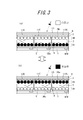
- (A), (b) is a figure which shows an example of the fundamental structure of the information display panel of this invention, respectively.
- (A), (b) is a figure which shows the other example of the fundamental structure of the information display panel of this invention, respectively.
- (A), (b) is a figure which shows the further another example of the fundamental structure of the information display panel of this invention, respectively. It is a figure for demonstrating the relationship which does not raise
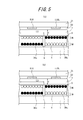
- (A), (b) is a figure for demonstrating an example of the formation method of the color filter in the information display panel of this invention, respectively.
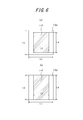
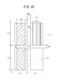
- (A), (b) is a figure for demonstrating the relationship of the area with respect to the pixel of the color filter used as the other characteristic of the information display panel of this invention, respectively. It is a figure for demonstrating the structure of an example of the information display panel of this invention which formed the dot-shaped color filter by inkjet printing. It is a figure for demonstrating the structure of an example of the information display panel of this invention which formed the stripe-shaped color filter by flexographic printing. It is a figure for demonstrating the structure of the other example of the information display panel of this invention which formed the dot-shaped color filter by inkjet printing. It is a figure for demonstrating the structure of the other example of the information display panel of this invention which formed the stripe-shaped color filter by flexographic printing.
- (A), (b) is a figure which shows an example of the example of arrangement
- (A), (b) is a figure which shows the other example of the example of arrangement
- an example of an information display panel using a particle group including a chargeable particle as a display medium in the information display panel of the present invention will be described.
- an electric field is applied to a display medium sealed in a space between two opposing substrates.
- the display medium is attracted by an electric field force or a Coulomb force, and the display medium is moved by a change in the electric field direction, whereby information such as an image is displayed. Therefore, it is necessary to design the display panel so that the display medium can move uniformly and maintain the stability when the display information is rewritten or when the display information is continuously displayed.
- the force applied to the particles constituting the display medium in addition to the force attracting each other by the Coulomb force between the particles, an electric mirror image force between the electrode and the substrate, an intermolecular force, a liquid cross-linking force, gravity and the like can be considered.
- FIGS. 1 (a), 1 (b) to 3 (a) examples of information display panels that use a particle group containing a chargeable particle as a display medium are shown in FIGS. 1 (a), 1 (b) to 3 (a), A description will be given based on (b).
- FIGS. 1 (a) and 1 (b) at least two types of display media having different optical reflectivity and charging characteristics, which are configured as a particle group including particles having at least optical reflectivity and chargeability
- a white display medium 3W configured as a particle group including negatively charged white particles 3Wa
- a black display medium 3B configured as a particle group including positively charged black particles 3Ba
- a red color filter 11R, a green color filter 11G, and a blue color filter 11BL are provided outside the observation-side transparent substrate 2 corresponding to each pixel, and a protective layer 13 is further formed thereon.
- the pixels and cells are made to correspond one-to-one, the red color filter 11R, the green color filter 11G, and the blue color filter 11BL are formed corresponding to the pixels, and display is performed with three RGB pixels as one display unit. .
- the white display medium 3W is moved to the viewer side so that the viewer can visually recognize the combined light transmitted through the red color filter 11R, the green color filter 11G, and the blue color filter 11BL.
- the white display is performed, or the black display medium 3B is moved to the observer side as shown in FIG.
- the pixel electrode pairs and the cells are arranged in a matrix in a one-to-one correspondence to perform dot matrix display.
- the partition in front is abbreviate
- At least two types of display media having different optical reflectivity and charging characteristics configured as a particle group including particles having at least optical reflectivity and chargeability
- a white display medium 3W configured as a particle group including negatively charged white particles 3Wa
- a black display medium 3B configured as a particle group including positively charged black particles 3Ba
- each cell it is generated by applying a voltage between a pair of pixel electrodes formed by the electrodes 5 (striped electrodes) provided on the substrate 1 and the electrodes 6 (striped electrodes) provided on the substrate 2 crossing each other at right angles.
- the substrate is moved perpendicular to the substrates 1 and 2 according to the electric field.
- a red color filter 11R, a green color filter 11G, and a blue color filter 11BL are provided outside the observation-side transparent substrate 2 corresponding to each pixel, and a protective layer 13 is further formed thereon.
- the pixels and cells are made to correspond one-to-one, the red color filter 11R, the green color filter 11G, and the blue color filter 11BL are formed corresponding to the pixels, and display is performed with three RGB pixels as one display unit. .
- the white display medium 3W is moved to the viewer side so that the viewer can visually recognize the combined light transmitted through the red color filter 11R, the green color filter 11G, and the blue color filter 11BL.
- the white display is performed, or the black display medium 3B is moved to the observer side as shown in FIG.
- the pixel electrode pairs and the cells are arranged in a matrix in a one-to-one correspondence to perform dot matrix display.
- the partition in front is abbreviate
- the example of the information display panel of the charged particle gas movement method in which the cell space is filled with gas has been described.
- the cell space is evacuated or an insulating liquid is used instead of gas.
- an information display panel of the charged particle liquid moving type (electrophoresis type) using In this case, as shown in FIG. 3, charged particles having a structure in which a group of particles containing chargeable particles is sealed in a capsule 8 together with an insulating liquid 7 as display media 3W and 3B, without the partition walls 4 forming cells. It is also possible to use an information display panel of a liquid moving type (electrophoresis type).
- a transparent protective film 13 is used as a method of providing the color filter (11R, 11G, 11BL) on the observation side transparent substrate.
- the color filter may be arranged on the observation side transparent substrate 2 through the transparent adhesive layer, or the color filter is formed on the observation side transparent substrate 2;
- the protective layer 13 may be provided by sticking a transparent film with a transparent adhesive material prepared separately on the color filter with an adhesive material.
- the information display panel according to the present invention is characterized in that, in the information display panel having the above-described configuration, the color filter of each color is positioned outside the observation-side transparent substrate having a refractive index n and a thickness d and overlapping the pixel.
- the area where the color filter overlaps with the pixel so that there is a gap in the part that is at least perpendicular to the diagonal viewing direction, between the color filters with different color filters at least on either the upper or lower sides or the left and right sides of the color filter Provided with 50% or more and 100% or less of the pixel area, and the pixel pitch and inter-pixel space in the viewing direction are LS and DS, respectively, and the image displayed on the display medium is reflected light refracted in the 45 ° direction on the color filter surface
- FIG. 4 shows one characteristic of the information display panel according to the present invention, which occurs when the color filter of each color is viewed from an oblique direction by being arranged outside the observation-side transparent substrate having a refractive index n and a thickness d. It is a figure for demonstrating color mixing.
- the same members as those in the examples shown in FIGS. 1A, 1B to 3A, 3B are denoted by the same reference numerals, and the description thereof is omitted.
- the reflected light from the display medium (here, black particles) in the pixel corresponding to the red color filter 11R passes through the green color filter 11G when viewed from an oblique ⁇ direction.
- the reflected light transmitted through the observation-side transparent substrate 2 is schematically shown as being refracted at the interface between the green color filter 11G and the observation-side transparent substrate 2 and traveling in the ⁇ direction.
- the reflected light that has progressed through refraction at the interface between the transparent electrode and the observation-side transparent substrate 2 and the interface between the color filter and the protective layer will be seen. Since the deviation due to refraction is negligible because it is extremely thin compared to the thickness of the observation-side transparent substrate 2, only refraction at the interface between the observation-side transparent substrate 2 and the color filter is considered here.
- the case where the external environment on the observation side is the air layer (refractive index 1) without considering the protective layer is shown, and the refractive direction when the refractive index n is larger than 1 is shown. Even when a protective layer is disposed between the color filter and the air layer, the relationship between the reflected light from the display medium and the direction in which the reflected light is refracted at the interface is also shown.
- the color is mixed even if the interval between the color filters of different colors is narrowed as the transparent substrate is made of a material having a refractive index n and the refractive index (n) is large. Can be made difficult to occur.
- the distance from the surface of the display medium (particle) to the color filter surface is indicated by the sum of the thickness d of the transparent substrate and the thickness of the transparent conductive film, but the transparent conductive film thickness is about several hundred nm. Therefore, the distance from the surface of the display medium to the color filter surface may be considered to be the same as the thickness d of the observation-side transparent substrate having a thickness of several tens of ⁇ m to several hundreds of ⁇ m. In the example shown in FIG.
- t is the length of the portion where the pixel and the color filter do not overlap.
- t provided on both the left and right sides may be the same length or different lengths.
- the length is the same. It is preferable to do this.
- the inter-pixel space in the viewing direction when viewed from an oblique direction is DS
- the pixel pitch is LS.
- the partition walls forming the cells are provided in this inter-pixel space, and the width thereof is set to DS or less.
- a partition wall having a narrower width than the inter-pixel space DS is provided.
- the color recognized through the filter is not only the reflected light from the display medium (particles) in the G color display pixel but also the reflected light from the direction of the adjacent R color display pixel by the amount of the visual field deviation l. It will be. That is, the color that is recognized through the G color filter is a mixed color.
- the visual field shift l can be reduced by reducing the thickness d of the transparent substrate equivalent to the distance from the surface of the display medium to the color filter surface and increasing the refractive index n.
- the inter-pixel space DS or the space t between the color filter and the pixel is increased, the color mixture of reflected light from the display medium (particle) in the adjacent R color display pixel can be reduced.
- DS is increased with respect to (LS-DS)
- a clear image cannot be obtained because the space between pixels is too large.
- the space t between the color filter and the pixel is increased with respect to the pixel length (LS-DS)
- LS-DS a clear image cannot be obtained because the area of the color filter is too small with respect to the area of the pixel.
- l ⁇ 0.5 ⁇ (DS + LS) in the relationship between the refractive index n of the liquid crystal and the distance from the display medium surface to the color filter surface, that is, the thickness d of the transparent substrate it will be described later.
- FIGS. 5A and 5B are diagrams for explaining an example of a method for forming a color filter in the information display panel of the present invention.
- the example shown in FIG. 5A is a configuration in which a transparent protective film 21 on which a color filter is formed is disposed outside the observation-side transparent substrate 2 with a transparent adhesive material 22, and from the surface of the display medium (particles) in this case
- the distance to the color filter surface is indicated by the sum of the thickness d of the transparent substrate, the thickness of the transparent conductive film, and the thickness of the transparent adhesive material layer on the color filter.
- the transparent conductive film thickness is about several hundred nm and the transparent adhesive layer thickness on the color filter is about several hundred nm, the distance from the display medium surface to the color filter surface is several tens ⁇ m to several hundred ⁇ m. It can be considered that the thickness is substantially the same as the thickness d of the observation-side transparent substrate.
- the example shown in FIG. 5B is a configuration in which a transparent protective film 21 is arranged with a transparent adhesive material 22 after forming a color filter on the outside of the observation-side transparent substrate 2.
- the distance from the surface of the display medium (particles) to the color filter surface is indicated by the sum of the thickness d of the transparent substrate and the thickness of the transparent conductive film.
- the transparent conductive film thickness is about several hundred nm. Therefore, the distance from the surface of the display medium to the color filter surface is several tens to several hundreds of micrometers. It may be considered substantially the same as the thickness d of a certain observation-side transparent substrate.
- 6 (a) and 6 (b) are diagrams for explaining the relationship of the area to the pixel of the color filter, which is another feature of the information display panel of the present invention.
- 6 (a) and 6 (b) both show an arrangement example in the case where a gap with a pixel is provided on at least one side of the color filter. In FIG. A gap is provided. In FIG. 6B, the gap is provided only on the left and right sides.
- the lengths of the pixels are L1 and L2, for example, the lengths of the red color filter 11R are L3 and L4.
- the ratio of the area of the color filter to the area of the pixel can be obtained from ⁇ (L3 ⁇ L4) / (L1 ⁇ L2) ⁇ ⁇ 100 (%). As is clear from the examples shown below, it was found that when this calculated value was 50% or more, it was displayed as a color image with good color vividness.
- the information display panel of the present invention can be suitably used in any of the color filter arrangements shown in FIGS. 7 to 10, LL is a pixel arrangement pitch (long side direction), and LS is a pixel arrangement pitch (short side direction).
- FIG. 7 is a view for explaining the configuration of an example of the information display panel according to the present invention in which dot-like three color filters (11R, 11G, 1BL) are formed by ink jet printing.
- the space (dots) between the pixels of the present invention is used as a condition for providing an information display panel that can obtain a good color display when viewed from the front and the diagonal direction on either side.
- Space DS is DS1 in FIG. 7
- pixel pitch LS is LS in FIG. t1 and t2 may have the same width or different widths.
- the space DS between the pixels of the present invention is DS2 in FIG. Yes
- the pixel pitch LS is LL in FIG. t3 and t4 may have the same width or different widths.
- the visual field deviation l needs to satisfy l ⁇ 0.5 (DS + LS).
- FIG. 8 is a view for explaining the configuration of an example of the information display panel of the present invention in which stripe-shaped three color filters (11R, 11G, 11BL) are formed by flexographic printing.
- the space (dots) between the pixels of the present invention can be used as a condition for providing an information display panel that can provide a good color display when viewed from the front and from the left and right diagonal directions.
- Space DS is DS1 in FIG. 8
- pixel pitch LS is LS in FIG. t1 and t2 may have the same width or different widths.
- the color filter of the same color is arranged in the adjacent pixel even when viewed from the upper or lower diagonal direction, so that an information display panel that can obtain a good color display can be obtained.
- the space (dot space) DS between the pixels of the present invention is DS2 in FIG. 8, and the pixel pitch LS is LL in FIG. Both t3 and t4 are zero.
- FIG. 9 is a view for explaining the configuration of another example of the information display panel of the present invention in which four-color filters (11R, 11G, 11BL, 11T) in the form of square dots are formed by ink jet printing.
- the space (dots) between the pixels of the present invention can be used as a condition for providing an information display panel that can provide a good color display when viewed from the front and from the left and right diagonal directions.
- Space DS is DS1 in FIG. 9
- pixel pitch LS is LS1 in FIG.
- the space (dot space) DS between the pixels of the present invention is shown in FIG. 9 DS2 and the pixel pitch LS is LS2 in FIG.
- the visual field deviation l needs to satisfy l ⁇ 0.5 (DS + LS).
- t1 and t2 may have the same width or different widths.
- Both t3 and t4 may have the same width or different widths.
- FIG. 10 is a view for explaining the configuration of still another example of the information display panel of the present invention in which four color filters (11R, 11G, 11BL, 11T) in the form of square dots are formed by ink jet printing.
- the space (dots) between the pixels of the present invention can be used as a condition for providing an information display panel that can provide good color display when viewed from the front and from the left and right diagonal directions.
- Space DS is DS1 in FIG. 10
- pixel pitch LS is LS1 in FIG.
- the space (dot space) DS between the pixels of the present invention is shown in FIG. 10 DS2, and the pixel pitch LS is LS2 in FIG.
- the visual field deviation l needs to satisfy l ⁇ 0.5 (DS + LS).
- 9 is different from the example shown in FIG. 9 in that a gap t between the pixel and the color filter is not provided in the vertical direction of the color filter. That is, t3 and t4 in FIG. t1 and t2 may have the same width or different widths.
- color filters of three primary colors for example, RGB three colors
- R pixels, G pixels, and B pixels are arranged in a 1 ⁇ 3 matrix to form one display unit (FIGS. 11A and 11B).
- color filters of the same color are arranged on either the left or right or upper and lower adjacent pixels.
- the color filters of different colors are adjacent to the left, right, upper or lower
- the gap is provided on the left and right sides of the color filter, and the gap is not provided on the upper and lower sides.
- the display color of adjacent pixels may be mixed when viewed from an obliquely vertical direction. Even in this case, by applying the present invention, it is possible to obtain an information display panel that does not feel mixed colors when viewed from any oblique direction.
- the thickness of the observation side transparent substrate is preferably 200 ⁇ m or less. If the thickness exceeds 200 ⁇ m, it may be difficult to realize the information display panel of the present invention.
- the refractive index n of the observation-side transparent substrate is preferably 1.47 or more. If the refractive index is less than 1.47, it may be difficult to realize the information display panel of the present invention.
- the transparent substrate material having a refractive index of 1.47 or more includes glass having a refractive index of 1.47, polyethylene terephthalate (PET) having a refractive index of 1.65, polyethylene naphthalate (PEN) having a refractive index of 1.67, refraction.
- Triacetyl cellulose with a refractive index of 1.49
- PC Polycarbonate
- PES Polyethersulfone
- PMMA Polymethyl methacrylate with a refractive index of 1.49 to 1.55
- acrylic resins such as (PMMA).
- three color filters of R: red, G: green, B: blue, C: cyan, M: magenta, and Y: yellow are used for each pixel.
- These three pixels constitute one display unit to form a 3 ⁇ 1 matrix arrangement, or one display unit having four pixels, one pixel adjacent to the other three pixels and no color filter. It may be configured to have a 2 ⁇ 2 or 4 ⁇ 1 matrix arrangement.
- a color filter is prepared and arranged on the outer surface of the observation-side transparent substrate using a printing method or a photolithography method.
- the color filter is disposed outside the observation-side transparent substrate, not only the transparent substrate on which the conductive film (electrode) is formed, but also the precursor of the information display panel of the present application. Also on the observation side transparent substrate, a color filter can be produced and arranged on the outside of the observation side transparent substrate by using a printing method such as inkjet printing or flexographic printing or a photolithography method.
- a liquid resist agent or A photolithography technique using a dry film resist material is preferably used.
- Alfo NIT2 manufactured by Nichigo Morton
- PDF300 manufactured by Nippon Steel Chemical Co., Ltd.
- these dry film resist materials are blended with various pigments, a partition wall having a desired color can be obtained.
- the width of the partition wall portion for securing the gap between the panel substrates is in a range of 20 ⁇ m to 100 ⁇ m within a range not exceeding the space DS between the pixels of the present invention, and the width of the partition wall portion dedicated for cell formation is the same as that of the pixel of the present invention.
- a range of 5 ⁇ m to 30 ⁇ m is preferable within a range not exceeding the space DS with the pixel.
- the transparent conductive film material provided in the information display region of the observation-side transparent substrate may be indium tin oxide (ITO), indium oxide, zinc-doped indium oxide (IZO). ), Transparent conductive metal oxides such as aluminum-doped zinc oxide (AZO), antimony tin oxide (ATO), conductive tin oxide, and conductive zinc oxide, and transparent such as polyaniline, polypyrrole, polythiophene (PEDOT: PSS, etc.) Examples thereof include conductive polymers.
- the conductive film material provided in the information display region of the back side substrate may be transparent or not transparent, and may be indium tin oxide (ITO ), Indium oxide, zinc-doped indium oxide (IZO), aluminum-doped zinc oxide (AZO), antimony tin oxide (ATO), conductive tin oxide, conductive zinc oxide and other conductive metal oxides, polyaniline, polypyrrole, Examples thereof include conductive polymers such as polythiophene (such as PEDOT: PSS), metals such as gold, silver, copper, aluminum, nickel, and chromium, and alloys containing these metals as main components.
- ITO indium tin oxide
- IZO zinc-doped indium oxide
- AZO aluminum-doped zinc oxide
- ATO antimony tin oxide
- conductive tin oxide conductive zinc oxide and other conductive metal oxides
- polyaniline polypyrrole
- Examples thereof include conductive polymers such as polythiophene (such as PEDOT: PSS
- a method for forming a conductive film provided on a substrate a method of forming the above-described materials into a thin film by sputtering, vacuum deposition, CVD (chemical vapor deposition), coating, or the like, or metal foil (for example, rolled copper foil) is used.
- a laminating method or a method of applying a conductive agent mixed with a solvent or a synthetic resin binder is used.
- the above-mentioned material that can be patterned and is electrically conductive can be preferably used.
- the thickness of the conductive film provided in the information display region of the observation-side transparent substrate is preferably 0.01 ⁇ m to 10 ⁇ m, more preferably 0.05 ⁇ m to 5 ⁇ m, as long as the electrical conductivity can be secured and the light transmittance is not affected.
- the thickness of the conductive film provided outside the information display area of the observation-side transparent substrate and the conductive film provided on the back-side substrate is only required to ensure conductivity, and is preferably 0.01 ⁇ m to 10 ⁇ m, more preferably 0.05 ⁇ m to 5 ⁇ m. .
- a metal oxide-based transparent conductive material such as ITO suitable as a conductive film provided on the observation-side transparent substrate is less flexible than a metal material.
- the metal oxide-based transparent conductive film provided in the information display area of the observation-side transparent substrate is preferably used in combination with a thin metal wire in order to prevent disconnection in the transparent electrode material.
- the width of the fine metal wire is preferably 1 ⁇ m to 10 ⁇ m because it does not hinder display visibility.
- the metal material having a small electric resistance and excellent flexibility is preferably used. Also, the thickness of the conductive film provided outside the information display area of the observation side substrate and on the back side substrate is designed to be 0.01 ⁇ m to 10 ⁇ m from the viewpoint of electrical resistance, productivity, and cost.
- Black display medium 60 parts by weight of methyl methacrylate monomer (Kanto Chemical Reagent) and 40 parts by weight (about 25 mol%) of ethylene glycol dimethacrylate (Wako Pure Chemical Reagent) as a polyfunctional monomer having a plurality of polymerization reactive groups in one molecule 3 parts by weight of a nigrosine compound (Bontron N07: manufactured by Orient Chemical) as a charge control agent for charging and 5 parts by weight of carbon black (special black: manufactured by Degussa) as a black pigment are dispersed by a sand mill (acrylic and methacrylic).
- a nigrosine compound Bontron N07: manufactured by Orient Chemical
- carbon black special black: manufactured by Degussa
- White display medium 100 parts by weight of polymethylpentene polymer (TPX-R18: made by Mitsui Chemicals), 100 parts by weight of titanium dioxide (Taipaque CR-90: made by Ishihara Sangyo Co., Ltd.) as a colorant, and phenol-based condensation as a negatively charged charge control agent 5 parts by weight of the product (Bontron E89: manufactured by Orient Chemical Co., Ltd.) was melt-kneaded with a twin-screw kneader and finely pulverized with a jet mill (Lab Jet Mill IDS-LJ type: Nippon Pneumatic Co., Ltd.). MDS-2: NIPPON NEUMATIC INDUSTRY CO., LTD.
- Example 1 An electrode-patterned transparent glass substrate with an ITO film (thickness: 200 ⁇ m, refractive index: 1.47) is held on a 100 nm-thick ITO film with a substrate spacing of 50 ⁇ m and a matrix-shaped opening of 1000 ⁇ m ⁇ 1000 ⁇ m.
- a partition wall (rib) is formed with a width of 20 ⁇ m, and a color filter material is formed by an inkjet method in the center of the position corresponding to the region surrounded by the partition wall on the transparent glass substrate surface opposite to the surface on which the ITO film is formed.
- a color filter in which four colors (R, G, BL, T) are arranged in 2 ⁇ 2 was produced.
- a color filter was provided around each color filter so as to leave a gap of 100 ⁇ m with respect to the pixel size surrounded by the partition walls.
- a color filter having a smaller area than the pixel size was formed.
- a photocurable color filter material (ink) was used.
- the acrylic monomer DCP-A (dimethylol cyclodecane di-7 acrylate) manufactured by Kyoeisha Co., Ltd. was used.
- As a photoinitiator Irgacure 184 of Ciba Specialty Chemicals was used.
- Example 1 in the evaluation result 1 in which the visibility from the front direction was evaluated, a clear and good display state was obtained. Moreover, in the evaluation result 2 which evaluated the visibility from diagonal 45 degrees direction, the display state which does not feel color mixing was obtained, and it determined with it being favorable.
- Example 2 On a 100 nm thick ITO film of a transparent polyethylene terephthalate film (PET film) substrate (thickness: 125 ⁇ m, refractive index: 1.65) with an electrode patterned ITO film, the substrate spacing is maintained at 50 ⁇ m, and 150 ⁇ m ⁇ 300 ⁇ m A partition wall (rib) having a matrix opening is formed with a width of 30 ⁇ m, and a color filter material is flexographically placed at the center of the position corresponding to the area surrounded by the partition wall on the side opposite to the surface on which the ITO film is formed.
- PET film transparent polyethylene terephthalate film
- Example 2 the evaluation result 1 which evaluated the visibility from the front direction showed a clear and good display state. Moreover, in the evaluation result 2 which evaluated the visibility from diagonal 45 degrees direction, the display state which does not feel color mixing was obtained, and it determined with it being favorable.
- Example 3 An electrode-patterned transparent glass substrate with an ITO film (thickness: 200 ⁇ m, refractive index: 1.47) is held on a 100 nm-thick ITO film with a substrate spacing of 50 ⁇ m and a matrix-shaped opening of 500 ⁇ m ⁇ 500 ⁇ m.
- a partition wall (rib) was formed with a width of 50 ⁇ m, and a color filter was formed by a photolithographic method in the center of the position corresponding to the region surrounded by the partition wall on the transparent glass substrate surface opposite to the surface on which the ITO film was formed.
- the color filter surface of a polyethylene terephthalate film (PET film) with a thickness of 125 ⁇ m to be used as a transparent protective layer was bonded using a transparent adhesive material.
- the color filter was produced by exposing it using an exposure mask and developing it using an aqueous sodium carbonate solution so that the color filter was arranged at the center of the position corresponding to the pixel formed by the ITO electrode.
- a color filter in which four colors (R, G, BL, T) are arranged in 2 ⁇ 2 was sequentially manufactured.
- each color filter a color filter having a small area with respect to the pixel size surrounded by the partition walls was provided. At this time, the gap between the periphery of the pixel and the periphery of the color filter was set to 60 ⁇ m.
- Example 3 the evaluation result 1 which evaluated the visibility from the front direction showed a clear and good display state. Moreover, in the evaluation result 2 which evaluated the visibility from diagonal 45 degrees direction, the display state which does not feel color mixing was obtained, and it determined with it being favorable.
- Example 4 An electrode patterned transparent polyethylene terephthalate film (PET film) substrate (PET film) substrate (thickness: 125 ⁇ m, refractive index: 1.65) is maintained on a 100 nm thick ITO film at a substrate spacing of 50 ⁇ m, 1000 ⁇ m ⁇ 1000 ⁇ m A partition wall (rib) having a matrix-shaped opening is formed with a width of 70 ⁇ m, and a photolithographic method is applied to the central portion of the position corresponding to the region surrounded by the partition wall on the transparent glass substrate surface opposite to the surface on which the ITO film is formed. A color filter was formed.
- a negative photoresist agent in which a pigment for color filter is dispersed is applied to the region so as to have a film thickness of 2.0 ⁇ m with a slit coater, exposed using an exposure mask, and developed using an aqueous sodium carbonate solution.
- a color filter having a size almost the same as the pixel size is provided at the center of the position corresponding to the pixel formed by the ITO electrode.
- three color filters of red, blue, and green are sequentially formed on three of the four pixels arranged in 2 ⁇ 2, and the color filter pigment is dispersed on one pixel.
- a transparent color filter T was formed without applying a negative photoresist agent.
- Example 4 in the evaluation result 1 in which the visibility from the front direction was evaluated, a clear and good display state was obtained. Moreover, in the evaluation result 2 which evaluated the visibility from diagonal 45 degrees direction, the display state which does not feel color mixing was obtained, and it determined with it being favorable.
- Example 5 On a 100 nm thick ITO film of a transparent polyethylene terephthalate film (PET film) substrate with electrode patterned ITO film (thickness: 25 ⁇ m, refractive index: 1.65), the substrate spacing is maintained at 50 ⁇ m, and 100 ⁇ m ⁇ 100 ⁇ m A partition wall (rib) having a matrix opening is formed with a width of 20 ⁇ m, and a color is formed at the center of the position corresponding to the region surrounded by the partition wall on the transparent PET film substrate surface opposite to the surface on which the ITO film is formed.
- PET film transparent polyethylene terephthalate film
- a filter material was formed by an ink jet method to produce a color filter in which four colors (red: R, green: G, blue: BL, transparent: T) were arranged in 2 ⁇ 2.
- a color filter having the same size as the pixel size surrounded by the partition walls was provided.
- the color filter was provided so as to leave a slight gap with the periphery of the pixel without exceeding at least the periphery of the pixel.
- a color filter having a size not exceeding the pixel size of 100 ⁇ m ⁇ 100 ⁇ m was formed by using ink droplets controlled to picoliter.
- a photocurable color filter material (ink) was used.
- the acrylic monomer DCP-A (dimethylol cyclodecane di-7 acrylate) manufactured by Kyoeisha Co., Ltd. was used.
- a photoinitiator Irgacure 184 of Ciba Specialty Chemicals was used.
- Example 5 in the evaluation result 1 in which the visibility from the front direction was evaluated, a clear and good display state was obtained. Moreover, in the evaluation result 2 which evaluated the visibility from diagonal 45 degrees direction, the display state which does not feel color mixing was obtained, and it determined with it being favorable.
- Example 6> A transparent polyethylene terephthalate film (PET film) substrate with electrode patterned ITO (thickness: 50 ⁇ m, refractive index: 1.65) on the ITO film, the substrate spacing is maintained at 50 ⁇ m, and a 100 ⁇ m ⁇ 100 ⁇ m matrix opening
- a partition wall (rib) having a portion is formed with a width of 20 ⁇ m, and a color filter material is provided at the center of the position corresponding to the region surrounded by the partition wall on the transparent PET film substrate surface opposite to the surface on which the ITO film is formed.
- a color filter in which four colors (red: R, green: G, blue: BL, transparent: T) are arranged 2 ⁇ 2 was formed by an inkjet method.
- a gap of 10 ⁇ m was provided around each color filter with respect to the pixel size surrounded by the partition walls.
- Example 6 in the evaluation result 1 in which the visibility from the front direction was evaluated, a clear and good display state was obtained. Moreover, in the evaluation result 2 which evaluated the visibility from diagonal 45 degrees direction, the display state which does not feel color mixing was obtained, and it determined with it being favorable.
- Example 7 A transparent polyethylene terephthalate film (PET film) substrate with electrode patterned ITO (PET film) substrate (thickness: 125 ⁇ m, refractive index: 1.65) on the ITO film, with a substrate spacing of 50 ⁇ m, 300 ⁇ m ⁇ 300 ⁇ m matrix opening
- a partition wall (rib) having a portion is formed with a width of 20 ⁇ m, and a color filter material is provided at the center of the position corresponding to the region surrounded by the partition wall on the transparent PET film substrate surface opposite to the surface on which the ITO film is formed.
- a color filter in which four colors (red: R, green: G, blue: BL, transparent: T) are arranged 2 ⁇ 2 was formed by an inkjet method.
- a gap of 40 ⁇ m was provided around each color filter with respect to the pixel size surrounded by the partition walls.
- Example 7 in the evaluation result 1 in which the visibility from the front direction was evaluated, a clear and good display state was obtained. Moreover, in the evaluation result 2 which evaluated the visibility from diagonal 45 degrees direction, the display state which does not feel color mixing was obtained, and it determined with it being favorable.
- Example 8> A transparent PET film substrate with an electrode patterned ITO film (thickness: 50 ⁇ m, refractive index: 1.65), on a 100 nm thick ITO film, the substrate spacing is maintained at 50 ⁇ m, and a matrix-shaped opening of 100 ⁇ m ⁇ 300 ⁇ m is formed.
- a partition wall (rib) having a width of 20 ⁇ m is formed, and a color filter material is flexographically (letter-pressed) at the center of the position corresponding to the area surrounded by the partition wall on the transparent PET substrate surface opposite to the surface on which the ITO film is formed.
- Example 8 in the evaluation result 1 in which the visibility from the front direction was evaluated, a clear and good display state was obtained. Moreover, in the evaluation result 2 which evaluated the visibility from diagonal 45 degrees direction, the display state which does not feel color mixing was obtained, and it determined with it being favorable.
- Example 9 On the 100 nm thick ITO film of the transparent polyethylene terephthalate film (PET film) substrate with electrode patterned ITO film (thickness: 50 ⁇ m, refractive index: 1.65), the substrate spacing is kept at 50 ⁇ m, 100 ⁇ m ⁇ 100 ⁇ m A partition wall (rib) having a matrix opening is formed with a width of 20 ⁇ m, and a color is formed at the center of the position corresponding to the region surrounded by the partition wall on the transparent PET film substrate surface opposite to the surface on which the ITO film is formed.
- PET film transparent polyethylene terephthalate film
- a filter material was formed by an ink jet method to produce a color filter in which four colors (red: R, green: G, blue: BL, transparent: T) were arranged in 2 ⁇ 2.
- a gap of 10 ⁇ m was provided around each color filter with respect to the pixel size surrounded by the partition walls.
- Example 9 the evaluation result 1 which evaluated the visibility from the front direction showed a clear and good display state. Moreover, in the evaluation result 2 which evaluated the visibility from diagonal 45 degrees direction, the display state which does not feel color mixing was obtained, and it determined with it being favorable.
- An electrode-patterned transparent glass substrate with an ITO film (thickness: 200 ⁇ m, refractive index: 1.47) is held on a 100 nm-thick ITO film with a substrate spacing of 50 ⁇ m and a matrix-shaped opening of 500 ⁇ m ⁇ 500 ⁇ m.
- a color filter material is formed into dots by an inkjet method. Then, a color filter in which four colors (red: R, green: G, blue: BL, transparent: T) are arranged 2 ⁇ 2 was produced. Each color filter was provided in a circular dot shape having a diameter of 400 ⁇ m, and a gap of about 50 ⁇ m was provided around the pixel size surrounded by a partition wall.
- Example 10 in the evaluation result 1 in which the visibility from the front direction was evaluated, a clear and good display state was obtained. Moreover, in the evaluation result 2 which evaluated the visibility from diagonal 45 degrees direction, the display state which does not feel color mixing was obtained, and it determined with it being favorable.
- a partition (rib) having a matrix-like opening of 200 ⁇ m ⁇ 200 ⁇ m is formed with a width of 20 ⁇ m on the side of the substrate, maintained at 50 ⁇ m.
- a color filter material is formed on the part by an ink jet method, and a color filter in which 4 colors (red: R, green: G, blue: BL, transparent: T) are arranged in 2 ⁇ 2 is made. Made.
- a gap of 10 ⁇ m was provided around each color filter with respect to the pixel size surrounded by the partition walls.
- Example 11 the evaluation result 1 which evaluated the visibility from the front direction showed a clear and good display state. Moreover, in the evaluation result 2 which evaluated the visibility from diagonal 45 degrees direction, the display state which does not feel color mixing was obtained, and it determined with it being favorable.
- Example 12 An electrode-patterned transparent glass substrate with an ITO film (thickness: 200 ⁇ m, refractive index: 1.47) is held on a 100 nm-thick ITO film with a substrate spacing of 50 ⁇ m and a matrix-shaped opening of 500 ⁇ m ⁇ 500 ⁇ m.
- a partition wall (rib) is formed with a width of 50 ⁇ m, and a color filter material is arranged in an area corresponding to the central portion of the pixel on the transparent glass substrate surface opposite to the surface on which the ITO film is formed. A filter was produced. Although there was a slight gap between the produced color filter and the pixel, a color filter of almost the same size as the pixel was formed.
- Example 12 in the evaluation result 1 in which the visibility from the front direction was evaluated, a clear and good display state was obtained. Moreover, in the evaluation result 2 which evaluated the visibility from the diagonal 45 degree
- An electrode-patterned transparent glass substrate with an ITO film (thickness: 700 ⁇ m, refractive index: 1.47) on a 100-nm thick ITO film has a substrate spacing of 50 ⁇ m and has a matrix-like opening of 500 ⁇ m ⁇ 500 ⁇ m
- a partition wall (rib) is formed with a width of 50 ⁇ m, and a color filter material is formed by an inkjet method in the center of the position corresponding to the region surrounded by the partition wall on the transparent glass substrate surface opposite to the surface on which the ITO film is formed. Then, a color filter in which four colors (red: R, green: G, blue: BL, transparent: T) are arranged 2 ⁇ 2 was produced.
- each color filter a gap of 60 ⁇ m was provided for the pixel size surrounded by the partition walls.
- a color filter having a smaller area than the pixel was formed.
- a photocurable color filter material (ink) was used.
- the acrylic monomer DCP-A (dimethylol cyclodecane di-7 acrylate) manufactured by Kyoeisha Co., Ltd. was used.
- As a photoinitiator Irgacure 184 of Ciba Specialty Chemicals was used. None was provided on the color filter layer.
- Comparative Example 1 in the evaluation result 1 in which the visibility from the front direction was evaluated, a clear and good display state was obtained. On the other hand, in the evaluation result 2 in which the visibility from an oblique 45 ° direction was evaluated, it was determined that the display was a display state in which adjacent other colors were mixed and was defective.
- An electrode-patterned transparent glass substrate with an ITO film (thickness: 200 ⁇ m, refractive index: 1.47) is held on a 100 nm thick ITO film with a substrate spacing of 50 ⁇ m and a matrix-shaped opening of 100 ⁇ m ⁇ 100 ⁇ m.
- a partition wall (rib) is formed with a width of 20 ⁇ m, and a color filter material is disposed in an area corresponding to the central portion of the pixel on the transparent glass substrate surface opposite to the surface on which the ITO film is formed.
- a filter was produced.
- a color filter was formed such that a gap of 10 ⁇ m was formed between the produced color filter and the pixel.
- Comparative Example 2 in the evaluation result 1 in which the visibility from the front direction was evaluated, a clear and good display state was obtained. On the other hand, in the evaluation result 2 in which the visibility from an oblique 45 ° direction was evaluated, it was determined that the display was a display state in which adjacent other colors were mixed and was defective.
- An electrode patterned transparent PET substrate with an ITO film (thickness: 200 ⁇ m, refractive index: 1.65) is held on a 100 nm thick ITO film with a substrate spacing of 50 ⁇ m and a matrix-shaped opening of 100 ⁇ m ⁇ 100 ⁇ m.
- a partition wall (rib) is formed with a width of 20 ⁇ m, and a color filter material is formed by an inkjet method in a region corresponding to the central portion of the pixel on the transparent PET substrate surface opposite to the surface on which the ITO film is formed.
- a gap of 40 ⁇ m was provided around each color filter with respect to the pixel size surrounded by the partition walls.
- the evaluation result 1 in which the visibility from the front direction was evaluated was a blurred color display state.
- the evaluation result 2 which evaluated the visibility from the diagonal 45 degree direction it was determined that it was a display state in which adjacent other colors were mixed and was defective.
- the ratio of the area of the color filter to the area of the pixel is 50% or more and the visual field deviation l when observed from an oblique 45 ° direction is l ⁇ 0.5 (DS + LS).
- the evaluation result 1 in which the visibility from the front direction is evaluated can obtain a clear and good display state.
- an evaluation result 2 in which the visibility from an oblique 45 ° direction was evaluated it was found that a display state without color mixing was obtained.
- the information display panel of the present invention is a notebook computer, an electronic notebook, a portable information device called PDA (Personal Digital Assistants), a display unit of a mobile device such as a mobile phone or a handy terminal, an electronic paper such as an electronic book or an electronic newspaper. , Billboards such as signboards, posters, blackboards (whiteboards), electronic desk calculators, display units for home appliances, automotive products, card display units such as point cards, IC cards, electronic advertisements, information boards, electronic POPs (Point Of (Presence, “Point” of “Purchase” advertising), electronic price tag, electronic shelf label, electronic score, display unit of RF-ID device, as well as display unit of various electronic devices such as POS terminal, car navigation device, clock, etc.
- POPs Point Of (Presence, “Point” of “Purchase” advertising), electronic price tag, electronic shelf label, electronic score, display unit of RF-ID device, as well as display unit of various electronic devices such as POS terminal, car navigation device, clock
Landscapes
- Physics & Mathematics (AREA)
- Nonlinear Science (AREA)
- General Physics & Mathematics (AREA)
- Optics & Photonics (AREA)
- Health & Medical Sciences (AREA)
- Life Sciences & Earth Sciences (AREA)
- Chemical & Material Sciences (AREA)
- Chemical Kinetics & Catalysis (AREA)
- Electrochemistry (AREA)
- Molecular Biology (AREA)
- Electrochromic Elements, Electrophoresis, Or Variable Reflection Or Absorption Elements (AREA)
Abstract
Description
l=d×{sin2θ/(n2-sin2θ)}1/2 θ=45°・・・式(1)。
l=d×{sin2θ/(n2-sin2θ)}1/2 θ=45°・・・式(1)
ので、斜め方向から見たときでも隣接画素との混色を避け、色再現性が高いカラー表示を行うことができる情報表示用パネルを得ることができる。
l=d×{sin2θ/(n2-sin2θ)}1/2 θ=45°・・・式(1)
とした点にある。
メチルメタクリレートモノマー(関東化学試薬)60重量部、及び、1分子中に重合反応基を複数持つ多官能性モノマーとしてエチレングリコールジメタクリレート(和光純薬試薬)40重量部(約25mol%)に、正帯電の荷電制御剤としてニグロシン化合物(ボントロンN07:オリエント化学製)3重量部、及び、黒色顔料として、カーボンブラック(スペシャルブラック:デグッサ製)5重量部をサンドミルにより分散させ、(アクリル系及びメタクリル系)樹脂-炭化水素系樹脂ブロックコポリマー(モディパーF600:日本油脂製)5重量部を溶解させた後、さらに2重量部のラウリルパーオキサイド(パーロイルL:日本油脂製)を溶解させた液を、界面活性剤としてポリオキシエチレンアルキルエーテル硫酸ナトリウム(ラテムルE-118B:花王製)を0.5%添加した精製水に懸濁、重合させ、濾過、乾燥させた後、分級機(MDS-2:日本ニューマチック工業)を用いて平均粒子径9.2μmの正帯電性黒色粒子群を得た。実施例では、この黒色粒子群を黒色表示媒体として用いた。
ポリメチルペンテンポリマー(TPX-R18:三井化学社製)100重量部と、着色剤として二酸化チタン(タイペークCR-90:石原産業社製)100重量部と、負帯電の荷電制御剤としてフェノール系縮合物(ボントロンE89:オリエント化学製)5重量部とを2軸混練機により溶融混練し、ジェットミル(ラボジェットミルIDS-LJ型:日本ニューマチック(株)製)で細かく粉砕し、分級機(MDS-2:日本ニュ-マチック工業)を用いて分級し、溶融球状化装置(MR-10:日本ニュ-マチック工業)を用いて溶融球状化して得た、平均粒子径が、9.5μmの負帯電性の白色粒子群を得た。実施例では、この白色粒子群を白色表示媒体として用いた。
電極パターニングしたITO膜付き透明ガラス基板(厚さ:200μm、屈折率:1.47)の、100nm厚のITO膜上に、基板間隔を50μmに保持し、1000μm×1000μmのマトリックス状開口部を有する隔壁(リブ)を20μm幅で形成し、ITO膜が形成された面とは反対側の透明ガラス基板面の隔壁で囲まれた領域に対応する位置中央部に、カラーフィルター材をインクジェット方式で形成して、4色(R、G、BL、T)が2×2で配置されたカラーフィルターを作製した。各カラーフィルターの周囲には隔壁で囲まれた画素サイズに対して100μmの隙間を残すようにカラーフィルターを設けた。なお、インクジェット法においては、インク滴のサイズをターゲットであるカラーフィルター層形成領域のサイズにあわせて制御することが好ましいので、1000μm×1000μmのマトリックス状開口部(画素)に対して、6~30ピコリットルに制御したインク滴とすることで画素サイズより小面積のカラーフィルターを形成した。
カラーフィルター材には、光硬化型カラーフィルター材(インク)を用いた。アクリル系モノマーには、共栄社(株)のDCP-A(ジメチロールシクロデカンジ7クリレート)を用いた。光開始剤には、チバスペシャリティケミカルズのイルガキュア184を用いた。
電極パターニングしたITO膜付き透明ポリエチレンテレフタレートフィルム(PETフィルム)基板(厚さ:125μm、屈折率:1.65)の、100nm厚のITO膜上に、基板間隔を50μmに保持し、150μm×300μmのマトリックス状開口部を有する隔壁(リブ)を30μm幅で形成し、ITO膜が形成された面とは反対側の面の隔壁で囲まれた領域に対応する位置中央部に、カラーフィルター材をフレキソ(凸版)印刷法で80μm幅のライン状に形成して、赤(R)、青(BL)、緑(G)3色のカラーフィルターを、150μmの画素辺に対して両側に35μmの隙間を有するカラーフィルターとなるように形成した。フレキソインクの光開始剤にはチバスペシャリティケミカルズのイルガキュア184を用いた。このフレキソインクを用いて、ガラス基板上に順次ストライプ状のカラーフィルターを印刷した。アニロックスロールには500線のものを使用し、膜厚が1.5μmとなるように調整した。
電極パターニングしたITO膜付き透明ガラス基板(厚さ:200μm、屈折率:1.47)の、100nm厚のITO膜上に、基板間隔を50μmに保持し、500μm×500μmのマトリックス状開口部を有する隔壁(リブ)を50μm幅で形成し、ITO膜が形成された面とは反対側の透明ガラス基板面の隔壁で囲まれた領域に対応する位置中央部に、フォトリソ法でカラーフィルターを形成した透明保護層とする厚さ125μmのポリエチレンテレフタレートフィルム(PETフィルム)のカラーフィルター面を透明粘着材を用いて貼り合せた。
カラーフィルター用顔料を分散した、ネガ型フォトレジスト剤をスリットコータにより、膜厚2.0μmとなるように、透明ガラス基板のITO膜が形成された面とは反対の面に一様に塗布し、露光マスクを用いて露光し、炭酸ナトリウム水溶液を用いて現像することで、ITO電極により形成された画素に対応する位置の中央部にカラーフィルターが配置されるようにカラーフィルターを作製した。4色(R、G、BL、T)が2×2で配置されたカラーフィルターを順次作製した。各カラーフィルターの周囲には隔壁で囲まれた画素サイズに対して小面積でカラーフィルターを設けた。このとき画素周囲とカラーフィルター周囲との間の隙間は60μmに設けた。
電極パターニングしたITO膜付き透明ポリエチレンテレフタレートフィルム(PETフィルム)基板(厚さ:125μm、屈折率:1.65)の、100nm厚のITO膜上に、基板間隔を50μmに保持し、1000μm×1000μmのマトリックス状開口部を有する隔壁(リブ)を70μm幅で形成し、ITO膜が形成された面とは反対側の透明ガラス基板面の隔壁で囲まれた領域に対応する位置中央部に、フォトリソ法でカラーフィルターを形成した。カラーフィルター用顔料を分散した、ネガ型フォトレジスト剤をスリットコータにより、膜厚2.0μmとなるように前記領域に塗布し、露光マスクを用いて露光し、炭酸ナトリウム水溶液を用いて現像することで、ITO電極により形成された画素に対応する位置の中央部に画素サイズに対してほとんど同じ大きさでカラーフィルターを設けた。カラーフィルターは2×2で配置された4個の画素のうち3個の画素に赤、青、緑の3色のカラーフィルターを順次作製し、1個の画素にはカラーフィルター用顔料を分散したネガ型フォトレジスト剤を塗布せずに透明色カラーフィルターTとした。
電極パターニングしたITO膜付き透明ポリエチレンテレフタレートフィルム(PETフィルム)基板(厚さ:25μm、屈折率:1.65)の、100nm厚のITO膜上に、基板間隔を50μmに保持し、100μm×100μmのマトリックス状開口部を有する隔壁(リブ)を20μm幅で形成し、ITO膜が形成された面とは反対側の透明PETフィルム基板面の隔壁で囲まれた領域に対応する位置中央部に、カラーフィルター材をインクジェット方式で形成して、4色(赤:R、緑:G、青:BL、透明:T)が2×2で配置されたカラーフィルターを作製した。各カラーフィルターの周囲には隔壁で囲まれた画素サイズに対してほとんど同じ大きさでカラーフィルターを設けた。このとき画素周囲とカラーフィルター周囲との間の隙間はほとんどなく、カラーフィルターは少なくとも画素の周囲を越えることなく画素周囲と僅かに隙間を残すように設けた。なお、インクジェット法においては、インク滴のサイズをターゲットであるカラーフィルター層形成領域のサイズにあわせて制御することが好ましいので、100μm×100μmのマトリックス状開口部(画素)に対して、6~30ピコリットルに制御したインク滴とすることで画素サイズの100μm×100μmを超えない大きさのカラーフィルターを形成した。
カラーフィルター材には、光硬化型カラーフィルター材(インク)を用いた。アクリル系モノマーには、共栄社(株)のDCP-A(ジメチロールシクロデカンジ7クリレート)を用いた。光開始剤には、チバスペシャリティケミカルズのイルガキュア184を用いた。
電極パターニングしたITO膜付き透明ポリエチレンテレフタレートフィルム(PETフィルム)基板(厚さ:50μm、屈折率:1.65)の、ITO膜上に、基板間隔を50μmに保持し、100μm×100μmのマトリックス状開口部を有する隔壁(リブ)を20μm幅で形成し、ITO膜が形成された面とは反対側の透明PETフィルム基板面の隔壁で囲まれた領域に対応する位置中央部に、カラーフィルター材をインクジェット方式で形成して、4色(赤:R、緑:G、青:BL、透明:T)が2×2で配置されたカラーフィルターを作製した。各カラーフィルターの周囲には隔壁で囲まれた画素サイズに対して10μmの隙間を設けた。
電極パターニングしたITO膜付き透明ポリエチレンテレフタレートフィルム(PETフィルム)基板(厚さ:125μm、屈折率:1.65)の、ITO膜上に、基板間隔を50μmに保持し、300μm×300μmのマトリックス状開口部を有する隔壁(リブ)を20μm幅で形成し、ITO膜が形成された面とは反対側の透明PETフィルム基板面の隔壁で囲まれた領域に対応する位置中央部に、カラーフィルター材をインクジェット方式で形成して、4色(赤:R、緑:G、青:BL、透明:T)が2×2で配置されたカラーフィルターを作製した。各カラーフィルターの周囲には隔壁で囲まれた画素サイズに対して40μmの隙間を設けた。
電極パターニングしたITO膜付き透明PETフィルム基板(厚さ:50μm、屈折率:1.65)の、100nm厚のITO膜上に、基板間隔を50μmに保持し、100μm×300μmのマトリックス状開口部を有する隔壁(リブ)を20μm幅で形成し、ITO膜が形成された面とは反対側の透明PET基板面の隔壁で囲まれた領域に対応する位置中央部に、カラーフィルター材をフレキソ(凸版)印刷法で80μm幅のライン状に形成して、赤(R)、青(BL)、緑(G)3色のカラーフィルターを、100μmの画素辺に対して両側に10μmの隙間を有するカラーフィルターとなるように形成した。フレキソインクの光開始剤にはチバスペシャリティケミカルズのイルガキュア184を用いた。このフレキソインクを用いて、PET基板上に順次ストライプ状のカラーフィルターを印刷した。アニロックスロールには500線のものを使用し、膜厚が1.5μmとなるように調整した。
電極パターニングしたITO膜付き透明ポリエチレンテレフタレートフィルム(PETフィルム)基板(厚さ:50μm、屈折率:1.65)の、100nm厚のITO膜上に、基板間隔を50μmに保持し、100μm×100μmのマトリックス状開口部を有する隔壁(リブ)を20μm幅で形成し、ITO膜が形成された面とは反対側の透明PETフィルム基板面の隔壁で囲まれた領域に対応する位置中央部に、カラーフィルター材をインクジェット方式で形成して、4色(赤:R、緑:G、青:BL、透明:T)が2×2で配置されたカラーフィルターを作製した。各カラーフィルターの周囲には隔壁で囲まれた画素サイズに対して10μmの隙間を設けた。
電極パターニングしたITO膜付き透明ガラス基板(厚さ:200μm、屈折率:1.47)の、100nm厚のITO膜上に、基板間隔を50μmに保持し、500μm×500μmのマトリックス状開口部を有する隔壁(リブ)を70μm幅で形成した基板側に表示媒体とする粒子群を配置した後にもう一方のITO膜付き透明ガラス基板(厚さ:700μm)を貼り合せて構成したパネル構造体の観察面側基板(厚さ:200μm)のITO膜が形成された面とは反対側の透明ガラス基板面の隔壁で囲まれた領域に対応する位置中央部に、カラーフィルター材をインクジェット方式でドット状に形成して、4色(赤:R、緑:G、青:BL、透明:T)が2×2で配置されたカラーフィルターを作製した。各カラーフィルターは直径400μmの円形ドット状に設け、周囲には隔壁で囲まれた画素サイズに対して約50μmの隙間を設けた。
ガラス基板上に200μm×200μmのマトリックス状に画素を形成したTFT基板上に、基板間隔を50μmに保持し、200μm×200μmのマトリックス状開口部を有する隔壁(リブ)を20μm幅で形成した基板側に表示媒体とする粒子群を配置した後に、パターニングされていない100nm厚のべたITO膜付き透明PET基板(厚さ:50μm、屈折率:1.65)を貼り合せて構成したパネル構造体の観察面側の透明PET基板(厚さ:50μm)のITO膜が形成された面とは反対側の面に、もう一枚の背面側TFT基板上に形成された画素電極の領域に対応する位置中央部に、カラーフィルター材をインクジェット方式で形成して、4色(赤:R、緑:G、青:BL、透明:T)が2×2で配置されたカラーフィルターを作製した。各カラーフィルターの周囲には隔壁で囲まれた画素サイズに対して10μmの隙間を設けた。
電極パターニングしたITO膜付き透明ガラス基板(厚さ:200μm、屈折率:1.47)の、100nm厚のITO膜上に、基板間隔を50μmに保持し、500μm×500μmのマトリックス状開口部を有する隔壁(リブ)を50μm幅で形成し、ITO膜が形成された面とは反対側の透明ガラス基板面の、画素の中央部に対応する領域にカラーフィルター材をインクジェット方式で配置して、カラーフィルターを作製した。作製されたカラーフィルターと画素との間には僅かに隙間ができていたがほぼ画素と同じサイズのカラーフィルターが形成されていた。
電極パターニングしたITO膜付き透明ガラス基板(厚さ:700μm、屈折率:1.47)の、100nm厚のITO膜上に、基板間隔を50μmに保持し、500μm×500μmのマトリックス状開口部を有する隔壁(リブ)を50μm幅で形成し、ITO膜が形成された面とは反対側の透明ガラス基板面の隔壁で囲まれた領域に対応する位置中央部に、カラーフィルター材をインクジェット方式で形成して、4色(赤:R、緑:G、青:BL、透明:T)が2×2で配置されたカラーフィルターを作製した。各カラーフィルターの周囲には隔壁で囲まれた画素サイズに対して60μmの隙間を設けた。なお、インクジェット法においては、インク滴のサイズをターゲットであるカラーフィルター層形成領域のサイズにあわせて制御することが好ましいので、500μm×500μmのマトリックス状開口部(画素)に対して、6~30ピコリットルに制御したインク滴とすることで画素よりも小面積のカラーフィルターを形成した。
カラーフィルター材には、光硬化型カラーフィルター材(インク)を用いた。アクリル系モノマーには、共栄社(株)のDCP-A(ジメチロールシクロデカンジ7クリレート)を用いた。光開始剤には、チバスペシャリティケミカルズのイルガキュア184を用いた。カラーフィルター層の上には何も設けなかった。
電極パターニングしたITO膜付き透明ガラス基板(厚さ:200μm、屈折率:1.47)の、100nm厚のITO膜上に、基板間隔を50μmに保持し、100μm×100μmのマトリックス状開口部を有する隔壁(リブ)を20μm幅で形成し、ITO膜が形成された面とは反対側の透明ガラス基板面の、画素の中央部に対応する領域にカラーフィルター材をインクジェット方式で配置して、カラーフィルターを作製した。作製されたカラーフィルターと画素との間には10μmの隙間ができるようにしてカラーフィルターを形成した。
電極パターニングしたITO膜付き透明PET基板(厚さ:200μm、屈折率:1.65)の、100nm厚のITO膜上に、基板間隔を50μmに保持し、100μm×100μmのマトリックス状開口部を有する隔壁(リブ)を20μm幅で形成し、ITO膜が形成された面とは反対側の透明PET基板面の画素の中央部に対応する領域にカラーフィルター材をインクジェット方式で形成して、カラーフィルターを作製した。各カラーフィルターの周囲には隔壁で囲まれた画素サイズに対して40μmの隙間を設けた。

3W 白色表示媒体
3Wa 負帯電性白色粒子
3B 黒色表示媒体
3Ba 正帯電性黒色粒子
4 隔壁
5、6 電極
7 絶縁液体
8 カプセル
11R 赤色カラーフィルター
11G 緑色カラーフィルター
11BL 青色カラーフィルター
11T 無色カラーフィルター
12 接着剤
13 保護層
21 透明保護フィルム
22 透明粘着材層
Claims (7)
- 観察側透明基板と、透明であることを要しない背面側基板とを対向配置した基板間空間に、表示媒体を封入し、観察側から入射した光を表示媒体で反射させた反射光として、観察側透明基板に設けた各色のカラーフィルターを通して表示情報をカラー認識できるようにした情報表示用パネルであって、
前記各色のカラーフィルターを、屈折率n、厚さdの観察側透明基板の外側であって画素と重なる位置に、カラーフィルターの上下両側か左右両側かのいずれか少なくとも隣接するカラーフィルター色が異なるカラーフィルター間であって、斜め視認方向と直角をなす部分に隙間を持つように、カラーフィルターが画素と重なる面積を画素面積の50%以上100%以下で設けるとともに、視認方向での画素ピッチおよび画素間スペースをそれぞれLSおよびDSとし、表示媒体が表示する画像をカラーフィルター面で45°方向に屈折した反射光として視認したときに起こる、式(1)で示される視野ずれl、との関係が、l≦0.5×(DS+LS)であることを特徴とする情報表示用パネル:
l=d×{sin2θ/(n2-sin2θ)}1/2 θ=45°・・・式(1)。 - 前記各色のカラーフィルターと画素との間に隙間tを形成したとき、表示媒体が表示する画像をカラーフィルター面で45°方向に屈折した反射光として視認したときに起こる、前記式(1)で示される視野ずれl、との関係が、l≦DS+tであることを特徴とする請求項1に記載の情報表示用パネル。
- 透明基板の一方の面に、パターニングされた透明導電膜もしくはべた透明導電膜が形成され、前記いずれかの導電膜が形成された面とは反対面側に前記各色のカラーフィルターを配置したことを特徴とする請求項1または2に記載の情報表示用パネル。
- 前記観察側となる透明な基板の厚さdが、200μm以下であり、かつ、前記観察側となる透明な基板の屈折率nが1.47以上であることを特徴とする請求項1~3のいずれか1項に記載の情報表示用パネル。
- 前記観察側となる透明な基板の材料が、ガラス、ポリエチレンテレフタレート(PET)、ポリエチレンナフタレート(PEN)、トリアセチルセルロース(TAC)、ポリカーボネート(PC)、アクリル系樹脂のいずれかであることを特徴とする請求項1~4のいずれか1項に記載の情報表示用パネル。
- カラーフィルターは、三原色のカラーフィルターまたは三原色と無色透明との4色のカラーフィルターの何れかで構成されることを特徴とする請求項1~5のいずれか1項に記載の情報表示用パネル。
- 請求項1~6のいずれか1項に記載の情報表示用パネルであって、カラーフィルターが形成された透明な観察側基板と、もう一方の背面側基板との間に封入する表示媒体として、少なくとも光学的反射率と帯電性とを有する粒子を含んだ粒子群を用い、基板間に形成した電界により表示媒体を移動させて情報を表示するものであることを特徴とする情報表示用パネル。
Priority Applications (4)
| Application Number | Priority Date | Filing Date | Title |
|---|---|---|---|
| CN2010800366342A CN102483553A (zh) | 2009-06-17 | 2010-06-09 | 信息显示面板 |
| US13/378,741 US8582198B2 (en) | 2009-06-17 | 2010-06-09 | Information display panel |
| JP2011519529A JPWO2010146810A1 (ja) | 2009-06-17 | 2010-06-09 | 情報表示用パネル |
| EP10789193A EP2444841A4 (en) | 2009-06-17 | 2010-06-09 | INFORMATION DISPLAY SCREEN |
Applications Claiming Priority (2)
| Application Number | Priority Date | Filing Date | Title |
|---|---|---|---|
| JP2009144520 | 2009-06-17 | ||
| JP2009-144520 | 2009-06-17 |
Publications (1)
| Publication Number | Publication Date |
|---|---|
| WO2010146810A1 true WO2010146810A1 (ja) | 2010-12-23 |
Family
ID=43356143
Family Applications (1)
| Application Number | Title | Priority Date | Filing Date |
|---|---|---|---|
| PCT/JP2010/003855 Ceased WO2010146810A1 (ja) | 2009-06-17 | 2010-06-09 | 情報表示用パネル |
Country Status (6)
| Country | Link |
|---|---|
| US (1) | US8582198B2 (ja) |
| EP (1) | EP2444841A4 (ja) |
| JP (1) | JPWO2010146810A1 (ja) |
| KR (1) | KR20120034202A (ja) |
| CN (1) | CN102483553A (ja) |
| WO (1) | WO2010146810A1 (ja) |
Cited By (5)
| Publication number | Priority date | Publication date | Assignee | Title |
|---|---|---|---|---|
| WO2014030336A1 (ja) * | 2012-08-21 | 2014-02-27 | 凸版印刷株式会社 | 反射型表示パネル及びその製造方法 |
| CN104169791A (zh) * | 2012-03-27 | 2014-11-26 | 索尼公司 | 显示单元和电子设备 |
| CN104220927A (zh) * | 2012-03-23 | 2014-12-17 | 凸版印刷株式会社 | 彩色反射型显示装置及其制造方法 |
| JP2015072342A (ja) * | 2013-10-02 | 2015-04-16 | 凸版印刷株式会社 | 反射型カラーディスプレイ及び反射型カラーディスプレイの製造方法 |
| EP2762931A4 (en) * | 2011-09-30 | 2015-05-27 | Toppan Printing Co Ltd | Color filter and display device comprising same |
Families Citing this family (8)
| Publication number | Priority date | Publication date | Assignee | Title |
|---|---|---|---|---|
| JP6129696B2 (ja) * | 2013-09-11 | 2017-05-17 | デクセリアルズ株式会社 | アンダーフィル材、及びこれを用いた半導体装置の製造方法 |
| CN105487280A (zh) * | 2016-01-20 | 2016-04-13 | 京东方科技集团股份有限公司 | 一种彩膜基板及其制作方法 |
| CN106328016B (zh) * | 2016-09-29 | 2017-12-15 | 京东方科技集团股份有限公司 | 显示面板及其制造方法、显示装置 |
| CN108333847A (zh) * | 2018-02-26 | 2018-07-27 | 广州奥翼电子科技股份有限公司 | 一种彩色显示器件 |
| CN108873452B (zh) * | 2018-06-25 | 2021-04-23 | Tcl华星光电技术有限公司 | 液晶显示装置 |
| CN111061112B (zh) * | 2020-01-02 | 2023-02-17 | 上海天马微电子有限公司 | 显示面板及其制作方法、显示装置 |
| KR102781957B1 (ko) * | 2020-07-07 | 2025-03-18 | 삼성전자주식회사 | 디스플레이 모듈 및 그 제조 방법 |
| CN114624938B (zh) | 2020-12-08 | 2024-09-24 | 川奇光电科技(扬州)有限公司 | 彩色滤光层阵列及具有彩色滤光层阵列的彩色电泳显示器 |
Citations (4)
| Publication number | Priority date | Publication date | Assignee | Title |
|---|---|---|---|---|
| JPS61231586A (ja) * | 1985-04-05 | 1986-10-15 | 株式会社リコー | カラ−液晶表示装置 |
| JPH0922031A (ja) * | 1995-07-07 | 1997-01-21 | Seiko Epson Corp | 液晶装置 |
| JP2000194286A (ja) * | 1998-12-28 | 2000-07-14 | Fujitsu Ltd | カラ―表示装置 |
| JP2008083521A (ja) | 2006-09-28 | 2008-04-10 | Bridgestone Corp | 情報表示用パネル |
Family Cites Families (4)
| Publication number | Priority date | Publication date | Assignee | Title |
|---|---|---|---|---|
| JPH0655137U (ja) * | 1992-12-28 | 1994-07-26 | シチズン時計株式会社 | 液晶表示装置 |
| KR20030069285A (ko) * | 2002-02-19 | 2003-08-27 | 삼성전자주식회사 | 액정 표시 장치 |
| CN100510924C (zh) * | 2005-11-09 | 2009-07-08 | 株式会社普利司通 | 信息显示用面板 |
| EP1785767A1 (en) * | 2005-11-09 | 2007-05-16 | Bridgestone Corporation | Information display panel |
-
2010
- 2010-06-09 KR KR1020127001143A patent/KR20120034202A/ko not_active Ceased
- 2010-06-09 US US13/378,741 patent/US8582198B2/en not_active Expired - Fee Related
- 2010-06-09 WO PCT/JP2010/003855 patent/WO2010146810A1/ja not_active Ceased
- 2010-06-09 CN CN2010800366342A patent/CN102483553A/zh active Pending
- 2010-06-09 EP EP10789193A patent/EP2444841A4/en not_active Withdrawn
- 2010-06-09 JP JP2011519529A patent/JPWO2010146810A1/ja active Pending
Patent Citations (4)
| Publication number | Priority date | Publication date | Assignee | Title |
|---|---|---|---|---|
| JPS61231586A (ja) * | 1985-04-05 | 1986-10-15 | 株式会社リコー | カラ−液晶表示装置 |
| JPH0922031A (ja) * | 1995-07-07 | 1997-01-21 | Seiko Epson Corp | 液晶装置 |
| JP2000194286A (ja) * | 1998-12-28 | 2000-07-14 | Fujitsu Ltd | カラ―表示装置 |
| JP2008083521A (ja) | 2006-09-28 | 2008-04-10 | Bridgestone Corp | 情報表示用パネル |
Non-Patent Citations (1)
| Title |
|---|
| See also references of EP2444841A4 |
Cited By (10)
| Publication number | Priority date | Publication date | Assignee | Title |
|---|---|---|---|---|
| EP2762931A4 (en) * | 2011-09-30 | 2015-05-27 | Toppan Printing Co Ltd | Color filter and display device comprising same |
| CN104220927A (zh) * | 2012-03-23 | 2014-12-17 | 凸版印刷株式会社 | 彩色反射型显示装置及其制造方法 |
| JPWO2013141257A1 (ja) * | 2012-03-23 | 2015-08-03 | 凸版印刷株式会社 | カラー反射型表示装置及びその製造方法 |
| US10073317B2 (en) | 2012-03-23 | 2018-09-11 | Toppan Printing Co., Ltd. | Color reflective display and method of manufacturing the same |
| CN110376786A (zh) * | 2012-03-23 | 2019-10-25 | 凸版印刷株式会社 | 彩色反射型显示装置及其制造方法 |
| CN104169791A (zh) * | 2012-03-27 | 2014-11-26 | 索尼公司 | 显示单元和电子设备 |
| WO2014030336A1 (ja) * | 2012-08-21 | 2014-02-27 | 凸版印刷株式会社 | 反射型表示パネル及びその製造方法 |
| JPWO2014030336A1 (ja) * | 2012-08-21 | 2016-07-28 | 凸版印刷株式会社 | 反射型表示パネル及びその製造方法 |
| US10564508B2 (en) | 2012-08-21 | 2020-02-18 | Toppan Printing Co., Ltd. | Reflection-type display panel and method of producing the same |
| JP2015072342A (ja) * | 2013-10-02 | 2015-04-16 | 凸版印刷株式会社 | 反射型カラーディスプレイ及び反射型カラーディスプレイの製造方法 |
Also Published As
| Publication number | Publication date |
|---|---|
| KR20120034202A (ko) | 2012-04-10 |
| US20120127561A1 (en) | 2012-05-24 |
| EP2444841A1 (en) | 2012-04-25 |
| JPWO2010146810A1 (ja) | 2012-11-29 |
| CN102483553A (zh) | 2012-05-30 |
| US8582198B2 (en) | 2013-11-12 |
| EP2444841A4 (en) | 2012-12-26 |
Similar Documents
| Publication | Publication Date | Title |
|---|---|---|
| JPWO2010146810A1 (ja) | 情報表示用パネル | |
| EP2372447A1 (en) | Information display panel | |
| WO2009145255A1 (ja) | 電子ペーパー | |
| JP2009282064A (ja) | 情報表示用パネルの観察側基板、情報表示用パネルおよびそれらの製造方法 | |
| JP2009271147A (ja) | 情報表示用パネルの観察側基板、情報表示用パネルおよびそれらの製造方法 | |
| CN102681280A (zh) | 彩色电泳方式的显示介质面板 | |
| JP2011095339A (ja) | カラー表示型情報表示用パネル | |
| JP2008287172A (ja) | 情報表示用パネル | |
| JP2010145528A (ja) | カラー情報表示用パネルの製造方法およびカラー情報表示用パネル | |
| JP5116458B2 (ja) | 情報表示用パネルおよび情報表示用パネルの製造方法 | |
| JP2010256560A (ja) | カラー表示用ディスプレイパネルの製造方法およびカラー表示用ディスプレイパネル | |
| JP2011237544A (ja) | カラーフィルター基板、その製造方法およびカラー表示型情報表示用パネル | |
| JP4902956B2 (ja) | 情報表示用パネル及び情報表示装置 | |
| JP2009103886A (ja) | 情報表示用パネル | |
| JP2008145683A (ja) | カラーフィルター付きパネル基板の製造方法、カラーフィルター付きパネル基板および情報表示用パネル | |
| US20110176198A1 (en) | Dot matrix type information display panel | |
| JP4977426B2 (ja) | 情報表示用パネル | |
| WO2011070769A1 (ja) | 情報表示用パネルおよびその製造方法 | |
| WO2011089919A1 (ja) | 音響発生機能付き画像表示装置 | |
| JP2010145532A (ja) | カラー情報表示用パネルの製造方法およびカラー情報表示用パネル | |
| JP5032192B2 (ja) | 情報表示用パネル | |
| JP2009069405A (ja) | 情報表示用パネル | |
| JP2011170047A (ja) | カラー表示型情報表示用パネルの製造方法 | |
| JP2006154664A (ja) | 情報表示用パネル及び情報表示装置 | |
| JP2010122492A (ja) | 情報表示用パネルの製造方法および情報表示用パネル |
Legal Events
| Date | Code | Title | Description |
|---|---|---|---|
| WWE | Wipo information: entry into national phase |
Ref document number: 201080036634.2 Country of ref document: CN |
|
| 121 | Ep: the epo has been informed by wipo that ep was designated in this application |
Ref document number: 10789193 Country of ref document: EP Kind code of ref document: A1 |
|
| WWE | Wipo information: entry into national phase |
Ref document number: 2011519529 Country of ref document: JP |
|
| NENP | Non-entry into the national phase |
Ref country code: DE |
|
| WWE | Wipo information: entry into national phase |
Ref document number: 2010789193 Country of ref document: EP |
|
| ENP | Entry into the national phase |
Ref document number: 20127001143 Country of ref document: KR Kind code of ref document: A |
|
| WWE | Wipo information: entry into national phase |
Ref document number: 13378741 Country of ref document: US |