WO2010146884A1 - 半導体チップおよびその実装構造 - Google Patents
半導体チップおよびその実装構造 Download PDFInfo
- Publication number
- WO2010146884A1 WO2010146884A1 PCT/JP2010/051415 JP2010051415W WO2010146884A1 WO 2010146884 A1 WO2010146884 A1 WO 2010146884A1 JP 2010051415 W JP2010051415 W JP 2010051415W WO 2010146884 A1 WO2010146884 A1 WO 2010146884A1
- Authority
- WO
- WIPO (PCT)
- Prior art keywords
- protruding
- protruding electrode
- electrode group
- region
- semiconductor chip
- Prior art date
- Legal status (The legal status is an assumption and is not a legal conclusion. Google has not performed a legal analysis and makes no representation as to the accuracy of the status listed.)
- Ceased
Links
Images










Classifications
-
- H—ELECTRICITY
- H10—SEMICONDUCTOR DEVICES; ELECTRIC SOLID-STATE DEVICES NOT OTHERWISE PROVIDED FOR
- H10W—GENERIC PACKAGES, INTERCONNECTIONS, CONNECTORS OR OTHER CONSTRUCTIONAL DETAILS OF DEVICES COVERED BY CLASS H10
- H10W74/00—Encapsulations, e.g. protective coatings
- H10W74/01—Manufacture or treatment
- H10W74/012—Manufacture or treatment of encapsulations on active surfaces of flip-chip devices, e.g. forming underfills
-
- H—ELECTRICITY
- H10—SEMICONDUCTOR DEVICES; ELECTRIC SOLID-STATE DEVICES NOT OTHERWISE PROVIDED FOR
- H10W—GENERIC PACKAGES, INTERCONNECTIONS, CONNECTORS OR OTHER CONSTRUCTIONAL DETAILS OF DEVICES COVERED BY CLASS H10
- H10W74/00—Encapsulations, e.g. protective coatings
- H10W74/10—Encapsulations, e.g. protective coatings characterised by their shape or disposition
- H10W74/15—Encapsulations, e.g. protective coatings characterised by their shape or disposition on active surfaces of flip-chip devices, e.g. underfills
-
- H—ELECTRICITY
- H10—SEMICONDUCTOR DEVICES; ELECTRIC SOLID-STATE DEVICES NOT OTHERWISE PROVIDED FOR
- H10W—GENERIC PACKAGES, INTERCONNECTIONS, CONNECTORS OR OTHER CONSTRUCTIONAL DETAILS OF DEVICES COVERED BY CLASS H10
- H10W72/00—Interconnections or connectors in packages
- H10W72/071—Connecting or disconnecting
- H10W72/072—Connecting or disconnecting of bump connectors
-
- H—ELECTRICITY
- H10—SEMICONDUCTOR DEVICES; ELECTRIC SOLID-STATE DEVICES NOT OTHERWISE PROVIDED FOR
- H10W—GENERIC PACKAGES, INTERCONNECTIONS, CONNECTORS OR OTHER CONSTRUCTIONAL DETAILS OF DEVICES COVERED BY CLASS H10
- H10W72/00—Interconnections or connectors in packages
- H10W72/071—Connecting or disconnecting
- H10W72/073—Connecting or disconnecting of die-attach connectors
-
- H—ELECTRICITY
- H10—SEMICONDUCTOR DEVICES; ELECTRIC SOLID-STATE DEVICES NOT OTHERWISE PROVIDED FOR
- H10W—GENERIC PACKAGES, INTERCONNECTIONS, CONNECTORS OR OTHER CONSTRUCTIONAL DETAILS OF DEVICES COVERED BY CLASS H10
- H10W72/00—Interconnections or connectors in packages
- H10W72/071—Connecting or disconnecting
- H10W72/073—Connecting or disconnecting of die-attach connectors
- H10W72/07331—Connecting techniques
- H10W72/07332—Compression bonding, e.g. thermocompression bonding
-
- H—ELECTRICITY
- H10—SEMICONDUCTOR DEVICES; ELECTRIC SOLID-STATE DEVICES NOT OTHERWISE PROVIDED FOR
- H10W—GENERIC PACKAGES, INTERCONNECTIONS, CONNECTORS OR OTHER CONSTRUCTIONAL DETAILS OF DEVICES COVERED BY CLASS H10
- H10W72/00—Interconnections or connectors in packages
- H10W72/071—Connecting or disconnecting
- H10W72/074—Connecting or disconnecting of anisotropic conductive adhesives
-
- H—ELECTRICITY
- H10—SEMICONDUCTOR DEVICES; ELECTRIC SOLID-STATE DEVICES NOT OTHERWISE PROVIDED FOR
- H10W—GENERIC PACKAGES, INTERCONNECTIONS, CONNECTORS OR OTHER CONSTRUCTIONAL DETAILS OF DEVICES COVERED BY CLASS H10
- H10W72/00—Interconnections or connectors in packages
- H10W72/20—Bump connectors, e.g. solder bumps or copper pillars; Dummy bumps; Thermal bumps
- H10W72/221—Structures or relative sizes
- H10W72/227—Multiple bumps having different sizes
-
- H—ELECTRICITY
- H10—SEMICONDUCTOR DEVICES; ELECTRIC SOLID-STATE DEVICES NOT OTHERWISE PROVIDED FOR
- H10W—GENERIC PACKAGES, INTERCONNECTIONS, CONNECTORS OR OTHER CONSTRUCTIONAL DETAILS OF DEVICES COVERED BY CLASS H10
- H10W72/00—Interconnections or connectors in packages
- H10W72/20—Bump connectors, e.g. solder bumps or copper pillars; Dummy bumps; Thermal bumps
- H10W72/231—Shapes
- H10W72/232—Plan-view shape, i.e. in top view
-
- H—ELECTRICITY
- H10—SEMICONDUCTOR DEVICES; ELECTRIC SOLID-STATE DEVICES NOT OTHERWISE PROVIDED FOR
- H10W—GENERIC PACKAGES, INTERCONNECTIONS, CONNECTORS OR OTHER CONSTRUCTIONAL DETAILS OF DEVICES COVERED BY CLASS H10
- H10W72/00—Interconnections or connectors in packages
- H10W72/20—Bump connectors, e.g. solder bumps or copper pillars; Dummy bumps; Thermal bumps
- H10W72/241—Dispositions, e.g. layouts
-
- H—ELECTRICITY
- H10—SEMICONDUCTOR DEVICES; ELECTRIC SOLID-STATE DEVICES NOT OTHERWISE PROVIDED FOR
- H10W—GENERIC PACKAGES, INTERCONNECTIONS, CONNECTORS OR OTHER CONSTRUCTIONAL DETAILS OF DEVICES COVERED BY CLASS H10
- H10W72/00—Interconnections or connectors in packages
- H10W72/20—Bump connectors, e.g. solder bumps or copper pillars; Dummy bumps; Thermal bumps
- H10W72/241—Dispositions, e.g. layouts
- H10W72/247—Dispositions of multiple bumps
- H10W72/248—Top-view layouts, e.g. mirror arrays
-
- H—ELECTRICITY
- H10—SEMICONDUCTOR DEVICES; ELECTRIC SOLID-STATE DEVICES NOT OTHERWISE PROVIDED FOR
- H10W—GENERIC PACKAGES, INTERCONNECTIONS, CONNECTORS OR OTHER CONSTRUCTIONAL DETAILS OF DEVICES COVERED BY CLASS H10
- H10W72/00—Interconnections or connectors in packages
- H10W72/20—Bump connectors, e.g. solder bumps or copper pillars; Dummy bumps; Thermal bumps
- H10W72/261—Functions other than electrical connecting
-
- H—ELECTRICITY
- H10—SEMICONDUCTOR DEVICES; ELECTRIC SOLID-STATE DEVICES NOT OTHERWISE PROVIDED FOR
- H10W—GENERIC PACKAGES, INTERCONNECTIONS, CONNECTORS OR OTHER CONSTRUCTIONAL DETAILS OF DEVICES COVERED BY CLASS H10
- H10W72/00—Interconnections or connectors in packages
- H10W72/20—Bump connectors, e.g. solder bumps or copper pillars; Dummy bumps; Thermal bumps
- H10W72/261—Functions other than electrical connecting
- H10W72/263—Providing mechanical bonding or support, e.g. dummy bumps
-
- H—ELECTRICITY
- H10—SEMICONDUCTOR DEVICES; ELECTRIC SOLID-STATE DEVICES NOT OTHERWISE PROVIDED FOR
- H10W—GENERIC PACKAGES, INTERCONNECTIONS, CONNECTORS OR OTHER CONSTRUCTIONAL DETAILS OF DEVICES COVERED BY CLASS H10
- H10W72/00—Interconnections or connectors in packages
- H10W72/20—Bump connectors, e.g. solder bumps or copper pillars; Dummy bumps; Thermal bumps
- H10W72/261—Functions other than electrical connecting
- H10W72/267—Multiple bump connectors having different functions
-
- H—ELECTRICITY
- H10—SEMICONDUCTOR DEVICES; ELECTRIC SOLID-STATE DEVICES NOT OTHERWISE PROVIDED FOR
- H10W—GENERIC PACKAGES, INTERCONNECTIONS, CONNECTORS OR OTHER CONSTRUCTIONAL DETAILS OF DEVICES COVERED BY CLASS H10
- H10W72/00—Interconnections or connectors in packages
- H10W72/30—Die-attach connectors
- H10W72/321—Structures or relative sizes of die-attach connectors
- H10W72/325—Die-attach connectors having a filler embedded in a matrix
-
- H—ELECTRICITY
- H10—SEMICONDUCTOR DEVICES; ELECTRIC SOLID-STATE DEVICES NOT OTHERWISE PROVIDED FOR
- H10W—GENERIC PACKAGES, INTERCONNECTIONS, CONNECTORS OR OTHER CONSTRUCTIONAL DETAILS OF DEVICES COVERED BY CLASS H10
- H10W72/00—Interconnections or connectors in packages
- H10W72/30—Die-attach connectors
- H10W72/351—Materials of die-attach connectors
-
- H—ELECTRICITY
- H10—SEMICONDUCTOR DEVICES; ELECTRIC SOLID-STATE DEVICES NOT OTHERWISE PROVIDED FOR
- H10W—GENERIC PACKAGES, INTERCONNECTIONS, CONNECTORS OR OTHER CONSTRUCTIONAL DETAILS OF DEVICES COVERED BY CLASS H10
- H10W72/00—Interconnections or connectors in packages
- H10W72/30—Die-attach connectors
- H10W72/351—Materials of die-attach connectors
- H10W72/353—Materials of die-attach connectors not comprising solid metals or solid metalloids, e.g. ceramics
- H10W72/354—Materials of die-attach connectors not comprising solid metals or solid metalloids, e.g. ceramics comprising polymers
-
- H—ELECTRICITY
- H10—SEMICONDUCTOR DEVICES; ELECTRIC SOLID-STATE DEVICES NOT OTHERWISE PROVIDED FOR
- H10W—GENERIC PACKAGES, INTERCONNECTIONS, CONNECTORS OR OTHER CONSTRUCTIONAL DETAILS OF DEVICES COVERED BY CLASS H10
- H10W72/00—Interconnections or connectors in packages
- H10W72/30—Die-attach connectors
- H10W72/381—Auxiliary members
- H10W72/387—Flow barriers
-
- H—ELECTRICITY
- H10—SEMICONDUCTOR DEVICES; ELECTRIC SOLID-STATE DEVICES NOT OTHERWISE PROVIDED FOR
- H10W—GENERIC PACKAGES, INTERCONNECTIONS, CONNECTORS OR OTHER CONSTRUCTIONAL DETAILS OF DEVICES COVERED BY CLASS H10
- H10W90/00—Package configurations
- H10W90/701—Package configurations characterised by the relative positions of pads or connectors relative to package parts
- H10W90/721—Package configurations characterised by the relative positions of pads or connectors relative to package parts of bump connectors
- H10W90/724—Package configurations characterised by the relative positions of pads or connectors relative to package parts of bump connectors between a chip and a stacked insulating package substrate, interposer or RDL
-
- H—ELECTRICITY
- H10—SEMICONDUCTOR DEVICES; ELECTRIC SOLID-STATE DEVICES NOT OTHERWISE PROVIDED FOR
- H10W—GENERIC PACKAGES, INTERCONNECTIONS, CONNECTORS OR OTHER CONSTRUCTIONAL DETAILS OF DEVICES COVERED BY CLASS H10
- H10W90/00—Package configurations
- H10W90/701—Package configurations characterised by the relative positions of pads or connectors relative to package parts
- H10W90/731—Package configurations characterised by the relative positions of pads or connectors relative to package parts of die-attach connectors
- H10W90/734—Package configurations characterised by the relative positions of pads or connectors relative to package parts of die-attach connectors between a chip and a stacked insulating package substrate, interposer or RDL
-
- H—ELECTRICITY
- H10—SEMICONDUCTOR DEVICES; ELECTRIC SOLID-STATE DEVICES NOT OTHERWISE PROVIDED FOR
- H10W—GENERIC PACKAGES, INTERCONNECTIONS, CONNECTORS OR OTHER CONSTRUCTIONAL DETAILS OF DEVICES COVERED BY CLASS H10
- H10W99/00—Subject matter not provided for in other groups of this subclass
Definitions
- the present invention relates to a semiconductor chip and a mounting structure thereof, and more particularly to a structure of a semiconductor chip mounted on a substrate using a conductive adhesive and a mounting structure of such a semiconductor chip on the substrate.
- flip chip mounting is known as a method for mounting a chip on a wiring board in a very small area.
- Flip chip mounting is a mounting method in which protruding electrodes called “bumps” are formed on the surface of a non-packaged chip called a “bare chip”, and the circuit board faces downward and is directly electrically connected to the wiring board. Is the method.
- an anisotropic conductive material is generally used for bonding the wiring board and the chip.
- the anisotropic conductive material is a connection material having conductivity in the thickness direction in the crimping portion and insulating in the surface direction in the crimping portion.
- the anisotropic conductive material is mainly composed of conductive particles and a resin functioning as an adhesive (hereinafter referred to as “adhesive resin”) (conductive particles are dispersed in the adhesive resin). .
- adhesive resin a resin functioning as an adhesive
- heat and pressure are applied to the bonded portion, so that the adhesive resin is spread.
- conductive particles are sandwiched (captured) between the opposing electrodes, whereby the opposing electrodes are electrically connected.
- the filling amount of the conductive particles into the adhesive resin is designed according to the connection area of the electrodes and the space between the electrodes.
- ACP Adisotropic Conductive Paste
- ACF Anaisotropic Conductive Film
- ACP and ACF are adhesives in which conductive particles such as nickel particles and gold-plated plastic particles are dispersed in an adhesive made of a thermosetting resin such as an epoxy resin.
- ACP and ACF are compared, the fluidity of the conductive particles is higher in ACP than in ACF. For this reason, ACP has the disadvantage that it is difficult to capture conductive particles between electrodes during bonding.
- the ACF has an advantage that conductive particles are easily captured between the electrodes at the time of bonding, and electrical conduction is reliably ensured.
- ACF is increasingly used as an adhesive from the viewpoint of easy capture of conductive particles.
- FIG. 15 is a bottom view of a conventional LSI chip 70 used as a drive circuit for a liquid crystal display device.
- an input bump group 710 composed of a plurality of input bumps (input terminals) 71 arranged in a line along one long side, and a zigzag arrangement along the other long side.
- the input bump group 710 and the output bump group 720 are connected to the electrode pads formed on the wiring board on which the LSI chip 70 is mounted by ACF.
- An electric signal for operating the LSI chip 70 is applied to the electrode pads connected to the input bump group 710. Scanning signal lines and video signal lines are connected to the electrode pads connected to the output bump group 720, and driving signals are given from the LSI chip 70 to the scanning signal lines and video signal lines via the electrode pads.
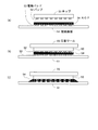
- FIG. 16A a wiring substrate 51 on which an electrode pad 53 for electrical connection with the chip 50 is formed and a chip 50 on which a bump 52 is formed are prepared.
- ACF 54 is affixed to wiring substrate 51 so as to cover the substrate.
- the crimping tool 55 performs thermocompression bonding of the chip 50 to the wiring substrate 51. The thermocompression bonding is performed in a state where the bumps 52 provided on the bottom surface of the chip 50 and the electrode pads 53 on the wiring substrate 51 are aligned.
- ACF resin the resin constituting the ACF 54
- the ACF resin flows out from the center of the chip 50 to the outside as shown in FIG.
- the conductive particles contained in the ACF resin ensure electrical conduction between the bumps 52 on the bottom surface of the chip 50 and the electrode pads 53 on the wiring substrate 51.
- Japanese Patent Application Laid-Open No. 2004-252466 discloses an invention of IC chips 80 and 85 having a bottom surface configured as shown in FIGS.
- reference numerals 81, 82, and 83 are assigned to the input bump group, the output bump group connected to the video signal line, and the output bump group connected to the scanning signal line, respectively.
- reference numerals 86, 87, and 88 are assigned to the input bump group, the output bump group connected to the video signal line, and the output bump group connected to the scanning signal line, respectively.
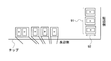
- Japanese Patent Laid-Open No. 2006-106132 discloses a configuration in which a test terminal group 91 is provided on the short side of a chip as shown in FIG. 19 and a center side of an input terminal group 93 as shown in FIG. Discloses a configuration including a test terminal group 94.
- FIG. 20 is a partially enlarged view of a region indicated by reference numeral 95 in FIG.
- Japanese Unexamined Patent Application Publication No. 2007-173738 discloses a technique for preventing the entry of bubbles generated in the sealing resin into the wiring conductor by providing a dummy wiring conductor portion.
- FIG. 22 is a diagram for explaining the flow of the ACF resin on the bottom surface of the LSI chip 70 when the terminals of the LSI chip 70 shown in FIG. 15 are narrowed.
- the flow of the ACF resin is represented by the direction of the arrow, and the magnitude (flow rate) of the flow of the ACF resin is represented by the width of the arrow.
- the flow from the center to the short side has a very large flow rate as indicated by the arrow 75 because no bump is provided in the area between the input bump 71 and the output bump 72.
- the flow toward the output bump 72 side becomes smaller as it approaches the corner from the center of the long side as indicated by arrows 76 to 78.
- the ACF resin hardly flows between the output bumps 72 because the output bumps 72 are arranged in a staggered pattern at a narrow pitch.
- the flow rate from the central portion to the long side decreases as the flow rate from the central portion to the short side increases as described above.
- the flow rate is very small as indicated by the arrow 78.
- the above-described connection failure occurs in the vicinity of the corner portion. Since the input bumps 71 are not as narrow as the output bumps 72, the flow from the center to the long side of the flow toward the input bumps 71 is indicated by arrows 79 in the vicinity of the corner. As described above, a flow rate that does not cause poor connection is secured.
- an object of the present invention is to realize a semiconductor chip in which the pitch between terminals can be reduced, which can suppress the occurrence of a connection failure with a mounting destination substrate.
- a first aspect of the present invention is a first projecting electrode group having a rectangular bottom surface and comprising a plurality of projecting electrodes arranged along one long side of the bottom surface for receiving an input signal from the outside. And a second projecting electrode group comprising a plurality of projecting electrodes arranged along the other long side of the bottom surface and outputting an output signal to the outside, In the bottom surface, a region extending between the region where the first protruding electrode group is formed and the region where the second protruding electrode group is formed extends in a direction perpendicular to the long side of the bottom surface.
- a third projecting electrode group comprising a plurality of rectangular projecting electrodes having a long side as a side; The plurality of protruding electrodes included in the third protruding electrode group are electrodes that are not electrically connected to the outside.
- the plurality of protruding electrodes included in the third protruding electrode group includes only protruding electrodes formed near one short side and the other short side of the bottom surface.
- the long sides of the plurality of protruding electrodes included in the third protruding electrode group are between a region where the first protruding electrode group is formed and a region where the second protruding electrode group is formed. It is characterized by having a length of one-half or more of the distance.
- the third protruding electrode group includes a protruding electrode array including a plurality of protruding electrodes arranged in a line along a region where the first protruding electrode group is formed, and the second protruding electrode group. It is characterized by comprising a plurality of protruding electrode arrays including at least a protruding electrode array composed of a plurality of protruding electrodes arranged in a line along the region.
- the plurality of projecting electrodes included in the third projecting electrode group are relatively displaced to the other long side of the bottom surface relative to the projecting electrode disposed relatively to the one long side of the bottom surface.
- the protruding electrodes are arranged so as to be alternately arranged.
- the plurality of protruding electrodes included in the third protruding electrode group are formed such that long sides become longer as they approach the short side from the center of the bottom surface.
- the third protruding electrode group includes a protruding electrode array including a plurality of protruding electrodes arranged in a line along a region where the first protruding electrode group is formed, and the second protruding electrode group.
- a plurality of protruding electrodes arranged in a line along the region of the protruding electrode, The plurality of protruding electrodes included in each protruding electrode row are formed such that long sides become longer as they approach the short side from the center of the bottom surface.
- the second protruding electrode group is formed along a region where the protruding electrode array composed of a plurality of protruding electrodes arranged in a line along one long side of the bottom surface and the third protruding electrode group are formed. It is characterized by comprising a plurality of protruding electrode arrays including at least a protruding electrode array composed of a plurality of protruding electrodes arranged in a line.
- a liquid crystal module including a liquid crystal panel including first and second substrates facing each other, wherein a driving circuit for driving the liquid crystal panel is provided on the first substrate.
- a semiconductor chip according to any one of the first to eighth aspects of the present invention is mounted on the first substrate using an anisotropic conductive film as the drive circuit.
- a tenth aspect of the present invention is a mounting structure in which a semiconductor chip having a rectangular bottom surface is mounted on a wiring board on which electrical wiring is formed using an anisotropic conductive film, The semiconductor chip is disposed along one long side of the bottom surface, and includes a first protruding electrode group including a plurality of protruding electrodes for receiving an input signal from an electric wiring on the wiring board, and the other bottom surface.
- a second protruding electrode group consisting of a plurality of protruding electrodes arranged along the long side of the wiring board for outputting an output signal to the electric wiring on the wiring board, and an area where the first protruding electrode group is formed And a plurality of rectangular projecting electrodes having long sides extending in a direction perpendicular to the long side of the bottom surface, and arranged in a region between the first protruding electrode group and the region where the second protruding electrode group is formed.
- 3 protruding electrode groups, The plurality of protruding electrodes included in the third protruding electrode group are electrodes that are not electrically connected to the electric wiring on the wiring board.
- An eleventh aspect of the present invention is the tenth aspect of the present invention,
- the plurality of protruding electrodes included in the third protruding electrode group includes only protruding electrodes formed near one short side and the other short side of the bottom surface.
- a twelfth aspect of the present invention is the tenth aspect of the present invention,
- the long sides of the plurality of protruding electrodes included in the third protruding electrode group are between a region where the first protruding electrode group is formed and a region where the second protruding electrode group is formed. It is characterized by having a length of one-half or more of the distance.
- the third protruding electrode group includes a protruding electrode array including a plurality of protruding electrodes arranged in a line along a region where the first protruding electrode group is formed, and the second protruding electrode group. It is characterized by comprising a plurality of protruding electrode arrays including at least a protruding electrode array composed of a plurality of protruding electrodes arranged in a line along the region.
- a fourteenth aspect of the present invention is the tenth aspect of the present invention,
- the plurality of projecting electrodes included in the third projecting electrode group are relatively displaced to the other long side of the bottom surface relative to the projecting electrode disposed relatively to the one long side of the bottom surface.
- the protruding electrodes are arranged so as to be alternately arranged.
- a fifteenth aspect of the present invention is the tenth aspect of the present invention.
- the plurality of protruding electrodes included in the third protruding electrode group are formed such that long sides become longer as they approach the short side from the center of the bottom surface.
- a sixteenth aspect of the present invention is the tenth aspect of the present invention
- the third protruding electrode group includes a protruding electrode array including a plurality of protruding electrodes arranged in a line along a region where the first protruding electrode group is formed, and the second protruding electrode group.
- a plurality of protruding electrodes arranged in a line along the region of the protruding electrode, The plurality of protruding electrodes included in each protruding electrode row are formed such that long sides become longer as they approach the short side from the center of the bottom surface.
- a seventeenth aspect of the present invention is the tenth aspect of the present invention
- the second protruding electrode group is formed along a region where the protruding electrode array composed of a plurality of protruding electrodes arranged in a line along one long side of the bottom surface and the third protruding electrode group are formed. It is characterized by comprising a plurality of protruding electrode arrays including at least a protruding electrode array composed of a plurality of protruding electrodes arranged in a line.
- the wiring board is one of two boards constituting a liquid crystal panel included in a liquid crystal module
- the semiconductor chip is a drive circuit for driving the liquid crystal panel.
- a third protruding electrode group which includes a plurality of protruding electrodes having long sides extending in a direction perpendicular to the long side of the bottom surface of the semiconductor chip.
- the plurality of protruding electrodes included in the third protruding electrode group do not have a function of electrical connection. For this reason, since an electrical signal is not exchanged through the plurality of protruding electrodes included in the third protruding electrode group, a plurality of conductive resins for inhibiting the flow of the conductive resin without considering a wiring pattern or the like.
- the protruding electrode can be disposed on the bottom surface of the semiconductor chip. As a result, the pitch between terminals in the semiconductor chip can be reduced without increasing the chip size.
- the protruding electrode for inhibiting the flow of the conductive resin is provided only in the vicinity of both short sides of the bottom surface of the semiconductor chip. For this reason, it is possible to flow a larger amount of conductive resin in the vicinity of the corner portion of the semiconductor chip without lowering the degree of freedom in designing the semiconductor chip. As a result, it is possible to suppress the occurrence of poor connection in the vicinity of the corner portion where the shortage of the flow rate of the conductive resin is most likely to occur while effectively suppressing the increase in chip size.
- the third aspect of the present invention on the bottom surface of the semiconductor chip, most of the flow of the conductive resin from the central portion to the short side is inhibited by the third protruding electrode. For this reason, the occurrence of poor connection due to the insufficient flow rate of the conductive resin in the vicinity of the corner portion of the semiconductor chip is more reliably suppressed.
- the flow of the conductive resin from the central portion to the short side of the bottom surface of the semiconductor chip is relatively effectively inhibited. Is done. For this reason, a sufficient flow of the conductive resin is ensured even in the vicinity of the corner portion of the semiconductor chip. Thereby, in a semiconductor chip with a limited length of the protruding electrode, occurrence of poor connection due to insufficient flow rate of the conductive resin is suppressed.
- the fifth aspect of the present invention similar to the fourth aspect of the present invention, in a semiconductor chip with a limited length of the protruding electrode, occurrence of poor connection due to insufficient flow rate of the conductive resin is suppressed.
- the flow of the conductive resin is effectively inhibited as it approaches the short side from the center.
- the area occupied by the third protruding electrode decreases as the distance from the short side approaches the center.
- the occurrence of poor connection due to the insufficient flow rate of the conductive resin is suppressed while securing a certain degree of freedom in designing the semiconductor chip. .
- the semiconductor chip in which the second protruding electrode group for outputting the output signal to the outside is constituted by a plurality of protruding electrode arrays, the same as in the first aspect of the present invention. The effect is obtained.
- a liquid crystal module is realized in which a semiconductor chip having the same effect as any one of the first to eighth aspects of the present invention is mounted on a substrate of a liquid crystal panel.
- FIG. 1 is a bottom view of an LSI chip according to a first embodiment of the present invention.
- 2 is a plan view of a liquid crystal module including the LSI chip according to the first embodiment.
- FIG. FIG. 2 is a sectional view taken along line AA in FIG. 1.
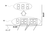
- a and B are diagrams for explaining the effects in the first embodiment. In the said 1st Embodiment, it is a figure for demonstrating the flow of ACF resin.
- a and B are diagrams for explaining the effects in the first embodiment. It is a bottom view of the LSI chip in the 2nd Embodiment of this invention. It is a bottom view of the LSI chip in the 3rd Embodiment of this invention.
- FIGS. 8A to 8C are diagrams for explaining mounting of a chip on a wiring board performed using an ACF. It is a bottom view of the conventional IC chip. It is a bottom view of the conventional IC chip. It is a bottom view of the conventional chip. It is the elements on larger scale of the bottom view of the conventional chip
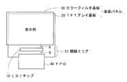
- FIG. 2 is a plan view of a liquid crystal module including an LSI chip (semiconductor chip) according to the first embodiment of the present invention.
- This liquid crystal module is composed of a liquid crystal panel, an LSI chip 10 and an FPC (Flexible Printed Circuit) 40.
- the liquid crystal panel applies a voltage between a TFT array substrate 20 including a pixel electrode (display electrode) and a TFT array formed thereon, and a color filter for color display and a pixel electrode through a liquid crystal layer.
- a color filter substrate 30 on which a counter electrode is formed. Both the TFT array substrate 20 and the color filter substrate 30 are glass substrates. As shown in FIG.
- the TFT array substrate 20 is larger than the color filter substrate 30 in plan view.
- a display unit is provided in a region where the TFT array substrate 20 and the color filter substrate 30 overlap in plan view.
- the region that does not face the color filter substrate 30 is generally called a “frame”.
- a liquid crystal panel driving LSI chip 10 is mounted in a frame area (hereinafter referred to as “frame area”) 21 and a controller for controlling the operation of the LSI chip 10. Etc. are connected, and thereby a liquid crystal module is realized.
- frame area a frame area
- COG Chip On Glass
- the color filter substrate 30 is illustrated in a slightly shifted upper left direction in plan view.
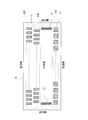
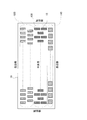
- FIG. 1 is a bottom view of the LSI chip 10 in the present embodiment.
- an input bump group 110 composed of a plurality of input bumps 11 arranged in a line along one long side, and a staggered pattern along the other long side.
- the output bump group 120 composed of a plurality of output bumps 12 arranged in a shape and the area where the input bump group 110 is provided and the area where the output bump group 120 is provided.
- a dummy bump group 130 including a plurality of dummy bumps 13 is also provided. Note that the dummy bumps 13 are bumps that do not have an electrical connection function.
- the input bump group 110 is connected to an electrode pad formed on the TFT array substrate 20 on which the LSI chip 10 is mounted by an ACF.
- An electric signal for operating the LSI chip 10 is applied to the electrode pads connected to the input bump group 110.
- the output bump group 120 is also connected to an electrode pad formed on the TFT array substrate 20 on which the LSI chip 10 is mounted by an ACF.
- a scanning signal line or a video signal line is connected to the electrode pad connected to the output bump group 120, and a driving signal is sent from the LSI chip 10 to the scanning signal line and the video signal line via the electrode pad.
- the first bump electrode group is realized by the input bump group 110
- the second bump electrode group is realized by the output bump group 120
- the third bump electrode group is realized by the dummy bump group 130. Has been.
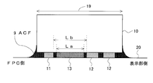
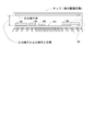
- FIG. 3 is a cross-sectional view taken along line AA in FIG. 1 (cross-sectional view taken along line BB in FIG. 2).
- an input bump 11 provided near one end (FPC side) of the bottom surface of the LSI chip 10 and an output bump 12 provided near the other end (display portion side) of the bottom surface of the LSI chip 10.
- a dummy bump 13 is provided between them.
- the TFT array substrate 20 and the LSI chip 10 are bonded to each other by the ACF 9.
- the length of the dummy bump 13 is the length of the input bump 11.
- the sheath is longer than the length of the output bump 12. Further, the length La of the long side of the dummy bump 13 is set as close as possible to the length Lb between the input bump 11 and the output bump 12 so that the flow of the ACF resin is inhibited as will be described later. For example, it is preferable that the La is half or more of the Lb. Further, it is more preferable that the La is 3/5 or more of the Lb. In FIG. 3, the electrode pads on the TFT array substrate 20 are omitted.
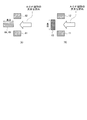
- the region between the input bump group 110 and the output bump group 120 is long in the vertical direction with respect to the large flow of ACF resin, as shown in FIG.
- a dummy bump group 130 including a plurality of dummy bumps 13 having sides is provided.
- FIG. 4B the flow of the ACF resin from the central portion to the short side is obstructed by the dummy bumps 13, and a larger amount of ACF resin is formed from the central portion to the long side than the conventional configuration. It flows to.
- a sufficient flow of the ACF resin is ensured even in the vicinity of the corner portion of the LSI chip 10, and the occurrence of poor connection due to the insufficient flow rate of the ACF resin is suppressed. .
- the bump denoted by reference numeral 84 can correspond to the dummy bump 13 in the present embodiment.
- the bump denoted by reference numeral 89 can correspond to the dummy bump 13 in the present embodiment.
- the dummy bumps 84 and 89 in the conventional configuration have long sides in the same direction as the large flow of the ACF resin as shown in FIG. As shown in B), it has a long side in a direction perpendicular to a large flow of the ACF resin.
- the flow direction of the ACF resin can be effectively changed to the long side (on the bottom surface of the LSI chip), and a sufficient amount of ACF resin can be formed in the vicinity of the corner portion of the LSI chip 10. The flow is ensured.
- dummy bumps 13 having no electrical connection function are employed as components for inhibiting the flow of the ACF resin. Since no electrical signal is exchanged via the dummy bumps 13, a plurality of dummy bumps 13 can be arranged on the bottom surface of the LSI chip 10 without considering a wiring pattern or the like. For this reason, the layout efficiency at the time of LSI design does not decrease, and the pitch between terminals can be narrowed without increasing the chip size. As a result, a liquid crystal module mounted with the LSI chip 10 with the terminals having a narrow pitch is realized.
- the LSI chip 10 in which the pitch between terminals is reduced in the liquid crystal module without imposing a heavy burden on the condition setting work in the connection process and the management work of the connection process. It becomes possible.
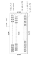
- FIG. 7 is a bottom view of the LSI chip 10 according to the second embodiment of the present invention.
- dummy bumps 13 are provided only near one short side and near the other short side of the bottom surface of the LSI chip 10. That is, only two dummy bumps 13 arranged on the outermost side among the plurality of dummy bumps 13 (see FIG. 1) included in the dummy bump group 130 in the first embodiment are formed on the bottom surface of the LSI chip 10. . Since other configurations are the same as those of the first embodiment, description thereof is omitted.
- the connection between the LSI chip 10 and the TFT array substrate 20 is increased. Reliability is increased.
- the degree of design freedom of the LSI chip 10 decreases. Therefore, as shown in FIG. 7, by providing the dummy bumps 13 only in the vicinity of both short sides of the bottom surface of the LSI chip 10, near the corner portion of the LSI chip 10 without reducing the design flexibility of the LSI chip 10. In this case, a sufficient amount of ACF resin can be ensured. As a result, it is possible to suppress the occurrence of poor connection in the vicinity of the corner portion where the ACF resin flow rate is most likely to be insufficient, while effectively suppressing the increase in chip size.
- FIG. 8 is a bottom view of the LSI chip 10 according to the third embodiment of the present invention.
- the length of the long side of the bump may be limited to a predetermined length or less.
- the distance between the input bump group 110 and the dummy bump group 130 or the distance between the output bump group 120 and the dummy bump group 130 becomes large, and a large flow of ACF resin from the central portion to the short side becomes large. It is thought that it is not inhibited. Therefore, in the present embodiment, as shown in FIG.
- the dummy bump group 130 is relatively located on the bottom surface of the LSI chip 10 relative to the dummy bumps 13 arranged so as to be shifted relative to one long side of the bottom surface of the LSI chip 10.
- the dummy bumps 13 are arranged so as to be alternately arranged on the other long side. Since other configurations are the same as those of the first embodiment, description thereof is omitted.
- the flow of the ACF resin from the central portion to the short side is relatively effectively inhibited. .
- a sufficient flow of the ACF resin is ensured even in the vicinity of the corner portion of the LSI chip 10, and the occurrence of poor connection due to the insufficient flow rate of the ACF resin is suppressed.
- a dummy bump group 130 is configured by a plurality of dummy bumps 13 arranged in a plurality of rows. You may do it. Specifically, in the configuration shown in FIG. 9, the dummy bump group 130 is arranged in a row along the output bump group 120 and a dummy bump row 131 including a plurality of dummy bumps 13 arranged in a row along the input bump group 110. And a dummy bump row 132 composed of a plurality of dummy bumps 13. In the configuration shown in FIG.
- the dummy bump group 130 includes a dummy bump row 131 including a plurality of dummy bumps 13 arranged in a line along the input bump group 110 and a plurality of dummy bumps 131 arranged in a line along the output bump group 120.
- a dummy bump row 132 made up of dummy bumps 13 and a dummy bump row 133 made up of a plurality of dummy bumps 13 arranged in a row between the two dummy bump rows 131 and 132 are constituted.
- the configuration shown in FIG. 8 may be combined with the configuration shown in FIG. 9 or FIG. 10, that is, the configuration shown in FIG. 11 or FIG.
- FIG. 13 is a bottom view of the LSI chip 10 according to the fourth embodiment of the present invention.
- the flow rate of the ACF resin is often secured to the extent that no connection failure occurs near the center of the long side of the bottom surface (reference numeral 76 arrow). Therefore, it is conceivable that the closer to the center, the lower the need to inhibit the flow of the ACF resin from the center to the short side. Therefore, in the present embodiment, as shown in FIG.
- the plurality of dummy bumps 13 included in the dummy bump group 130 are formed so that the long sides become longer from the center of the bottom surface of the LSI chip 10 toward the short side. ing. Since other configurations are the same as those of the first embodiment, description thereof is omitted.
- the occurrence of poor connection in the vicinity of the corner where the ACF resin flow rate is most likely to be insufficient is suppressed, but in this embodiment, the design flexibility of the LSI chip 10 is secured to some extent. Further, it is possible to suppress the occurrence of poor connection not only in the vicinity of the corner portion but also in the vicinity of the corner portion.
- the dummy bump group 130 is configured by two dummy bump rows, and a plurality of dummy bumps 13 included in each dummy bump row are short-sided from the center of the bottom surface of the LSI chip 10. You may form so that a long side may become long as it approaches the side.
- the input bump group 110 is composed of one row of bumps (a row of bumps composed of a plurality of input bumps 12 arranged in a row along one long side of the bottom surface of the LSI chip 10).
- the output bump group 120 includes two bump rows (along the region in which the bump row composed of the plurality of output bumps 12 arranged in a row along the other long side of the bottom surface of the LSI chip 10 and the dummy bump group 130 are formed).
- the present invention is not limited to this.
- the present invention can be applied as long as the input bump group 110 and the output bump group 120 are arranged along one long side and the other long side of the LSI chip 10, respectively.
Landscapes
- Wire Bonding (AREA)
- Liquid Crystal (AREA)
Abstract
Description
前記底面において、前記第1の突起電極群が形成されている領域と前記第2の突起電極群が形成されている領域との間の領域に、前記底面の長辺に対して垂直方向に延びる辺を長辺とする長方形状の複数の突起電極からなる第3の突起電極群を備え、
前記第3の突起電極群に含まれる複数の突起電極は、外部との電気的な接続がなされない電極であることを特徴とする。
前記第3の突起電極群に含まれる複数の突起電極は、前記底面の一方の短辺近傍および他方の短辺近傍に形成された突起電極のみからなることを特徴とする。
前記第3の突起電極群に含まれる複数の突起電極の長辺は、前記第1の突起電極群が形成されている領域と前記第2の突起電極群が形成されている領域との間の距離の2分の1以上の長さであることを特徴とする。
前記第3の突起電極群は、前記第1の突起電極群が形成されている領域に沿って一列に配置された複数の突起電極からなる突起電極列と前記第2の突起電極群が形成されている領域に沿って一列に配置された複数の突起電極からなる突起電極列とを少なくとも含む複数の突起電極列によって構成されていることを特徴とする。
前記第3の突起電極群に含まれる複数の突起電極は、相対的に前記底面の一方の長辺側にずれて配置された突起電極と相対的に前記底面の他方の長辺側にずれて配置された突起電極とが交互に配置されるように形成されていることを特徴とする。
前記第3の突起電極群に含まれる複数の突起電極は、前記底面の中央部から短辺側に近づくに従い長辺が長くなるように形成されていることを特徴とする。
前記第3の突起電極群は、前記第1の突起電極群が形成されている領域に沿って一列に配置された複数の突起電極からなる突起電極列と前記第2の突起電極群が形成されている領域に沿って一列に配置された複数の突起電極からなる突起電極列とを含み、
各突起電極列に含まれる複数の突起電極は、前記底面の中央部から短辺側に近づくに従い長辺が長くなるように形成されていることを特徴とする。
前記第2の突起電極群は、前記底面の一方の長辺に沿って一列に配置された複数の突起電極からなる突起電極列と前記第3の突起電極群が形成されている領域に沿って一列に配置された複数の突起電極からなる突起電極列とを少なくとも含む複数の突起電極列によって構成されていることを特徴とする。
本発明の第1から第8までのいずれかの局面に係る半導体チップが前記駆動回路として異方性導電膜を用いて前記第1の基板に実装されていることを特徴とする。
前記半導体チップは、前記底面の一方の長辺に沿って配置され前記配線基板上の電気配線からの入力信号を受け取るための複数の突起電極からなる第1の突起電極群と、前記底面の他方の長辺に沿って配置され出力信号を前記配線基板上の電気配線に出力するための複数の突起電極からなる第2の突起電極群と、前記第1の突起電極群が形成されている領域と前記第2の突起電極群が形成されている領域との間の領域に配置され前記底面の長辺に対して垂直方向に延びる辺を長辺とする長方形状の複数の突起電極からなる第3の突起電極群とを備え、
前記第3の突起電極群に含まれる複数の突起電極は、前記配線基板上の電気配線との電気的な接続がなされない電極であることを特徴とする。
前記第3の突起電極群に含まれる複数の突起電極は、前記底面の一方の短辺近傍および他方の短辺近傍に形成された突起電極のみからなることを特徴とする。
前記第3の突起電極群に含まれる複数の突起電極の長辺は、前記第1の突起電極群が形成されている領域と前記第2の突起電極群が形成されている領域との間の距離の2分の1以上の長さであることを特徴とする。
前記第3の突起電極群は、前記第1の突起電極群が形成されている領域に沿って一列に配置された複数の突起電極からなる突起電極列と前記第2の突起電極群が形成されている領域に沿って一列に配置された複数の突起電極からなる突起電極列とを少なくとも含む複数の突起電極列によって構成されていることを特徴とする。
前記第3の突起電極群に含まれる複数の突起電極は、相対的に前記底面の一方の長辺側にずれて配置された突起電極と相対的に前記底面の他方の長辺側にずれて配置された突起電極とが交互に配置されるように形成されていることを特徴とする。
前記第3の突起電極群に含まれる複数の突起電極は、前記底面の中央部から短辺側に近づくに従い長辺が長くなるように形成されていることを特徴とする。
前記第3の突起電極群は、前記第1の突起電極群が形成されている領域に沿って一列に配置された複数の突起電極からなる突起電極列と前記第2の突起電極群が形成されている領域に沿って一列に配置された複数の突起電極からなる突起電極列とを含み、
各突起電極列に含まれる複数の突起電極は、前記底面の中央部から短辺側に近づくに従い長辺が長くなるように形成されていることを特徴とする。
前記第2の突起電極群は、前記底面の一方の長辺に沿って一列に配置された複数の突起電極からなる突起電極列と前記第3の突起電極群が形成されている領域に沿って一列に配置された複数の突起電極からなる突起電極列とを少なくとも含む複数の突起電極列によって構成されていることを特徴とする。
前記配線基板は、液晶モジュールに含まれる液晶パネルを構成する2枚の基板のうちの一方の基板であって、
前記半導体チップは、前記液晶パネルを駆動するための駆動回路であることを特徴とする。
<1.1 液晶モジュールの構成>
図2は、本発明の第1の実施形態に係るLSIチップ(半導体チップ)を備えた液晶モジュールの平面図である。この液晶モジュールは、液晶パネルとLSIチップ10とFPC(Flexible Printed Circuit)40とによって構成されている。液晶パネルは、画素電極(表示電極)を含みTFTアレイが形成されたTFTアレイ基板20と、カラー表示用のカラーフィルタが形成されるとともに液晶層を介して画素電極との間に電圧を印加するための対向電極が形成されたカラーフィルタ基板30とによって構成されている。TFTアレイ基板20およびカラーフィルタ基板30はともにガラス基板である。また、図2に示すように、カラーフィルタ基板30よりもTFTアレイ基板20の方が平面視で大きくなっている。TFTアレイ基板20とカラーフィルタ基板30とが平面視で重なる領域に表示部が設けられている。TFTアレイ基板20上の領域のうちカラーフィルタ基板30とは対向していない領域は一般に「額縁」と呼ばれている。本実施形態においては、額縁となる領域(以下、「額縁エリア」という。)21には、液晶パネル駆動用のLSIチップ10が実装されるとともに、当該LSIチップ10の動作を制御するためのコントローラ等を含むFPC40が接続され、これにより、液晶モジュールが実現されている。このように、本実施形態においては、ガラス基板上にLSIチップ10が搭載された構成すなわちCOG(Chip On Glass)方式が採用されている。なお、図2では、説明の便宜上、カラーフィルタ基板30を平面視でやや左上方向にずらして図示している。
図1は、本実施形態におけるLSIチップ10の底面図である。図1に示すように、このLSIチップ10の底面には、一方の長辺に沿って一列に配置された複数個の入力バンプ11からなる入力バンプ群110と、他方の長辺に沿って千鳥状に配置された複数個の出力バンプ12からなる出力バンプ群120と、入力バンプ群110が設けられている領域と出力バンプ群120が設けられている領域との間の領域に一列に配置された複数個のダミーバンプ13からなるダミーバンプ群130とが設けられている。なお、ダミーバンプ13とは、電気的接続の機能を持たないバンプのことである。入力バンプ群110は、このLSIチップ10を搭載するTFTアレイ基板20上に形成された電極パッドとACFによって接続される。そして、その入力バンプ群110に接続される電極パッドには、このLSIチップ10を動作させるための電気信号が与えられる。出力バンプ群120も、このLSIチップ10を搭載するTFTアレイ基板20上に形成された電極パッドとACFによって接続される。そして、その出力バンプ群120に接続される電極パッドには走査信号線や映像信号線が接続され、当該電極パッドを介してこのLSIチップ10から走査信号線および映像信号線に駆動用の信号が与えられる。
図15に示した従来の構成によると、LSIチップ70の底面の一方の長辺に沿って一列に配置された入力バンプ群710と他方の長辺に沿って千鳥状に配置された出力バンプ群720との間の領域には、ACF樹脂の流れを阻害するようなバンプ等は設けられていなかった。このため、図4(A)に示すように、中央部から短辺側へのACF樹脂の流量と比較すると、中央部から長辺側へのACF樹脂の流量は著しく小さくなっていた。その結果、LSIチップ70のコーナー部近傍において、ACF樹脂の流量不足が顕著となり(図22参照)、反応不足や樹脂不足に起因して信頼性が十分な接続状態が得られず、接続不良が生じていた。これに対して、本実施形態に係る構成によると、入力バンプ群110と出力バンプ群120との間の領域には、図1に示すように、ACF樹脂の大きな流れに対して垂直方向に長辺を有する複数のダミーバンプ13からなるダミーバンプ群130が設けられている。このため、図4(B)に示すように、中央部から短辺側へのACF樹脂の流れがダミーバンプ13によって阻害され、従来の構成と比較して多量のACF樹脂が中央部から長辺側へと流れる。これにより、図5で符号15の矢印で示すように、LSIチップ10のコーナー部近傍においてもACF樹脂の充分な流れが確保され、ACF樹脂の流量不足に起因する接続不良の発生が抑制される。
図7は、本発明の第2の実施形態におけるLSIチップ10の底面図である。本実施形態においては、図7に示すように、LSIチップ10の底面の一方の短辺近傍および他方の短辺近傍にのみダミーバンプ13が設けられている。すなわち、上記第1の実施形態におけるダミーバンプ群130に含まれる複数のダミーバンプ13(図1参照)のうち最も外側に配置されている2個のダミーバンプ13のみがLSIチップ10の底面に形成されている。それ以外の構成については、上記第1の実施形態と同様であるので、説明を省略する。
図8は、本発明の第3の実施形態におけるLSIチップ10の底面図である。LSIチップ10の底面におけるバンプの形成に関しては様々な制限が課され得る。例えば、バンプの長辺の長さが所定の長さ以下に制限されることもある。このような場合、入力バンプ群110とダミーバンプ群130との間の距離あるいは出力バンプ群120とダミーバンプ群130との間の距離が大きくなり、中央部から短辺側へのACF樹脂の大きな流れが阻害されないことが考えられる。そこで、本実施形態においては、図8に示すように、ダミーバンプ群130は、相対的にLSIチップ10底面の一方の長辺側にずれて配置されたダミーバンプ13と相対的にLSIチップ10底面の他方の長辺側にずれて配置されたダミーバンプ13とが交互に配置されるように形成されている。それ以外の構成については、上記第1の実施形態と同様であるので、説明を省略する。
図13は、本発明の第4の実施形態におけるLSIチップ10の底面図である。図22に示したように、端子間が狭ピッチ化されたLSIチップ70においても、底面の長辺の中心付近では接続不良が生じない程度にACF樹脂の流量が確保されることが多い(符号76の矢印参照)。従って、中央部に近いほど、中央部から短辺側へのACF樹脂の流れを阻害する必要性が低いことが考えられる。そこで、本実施形態においては、図13に示すように、ダミーバンプ群130に含まれる複数のダミーバンプ13は、LSIチップ10底面の中央部から短辺側に近づくに従い長辺が長くなるように形成されている。それ以外の構成については、上記第1の実施形態と同様であるので、説明を省略する。
上記各実施形態においては、LSIチップ10が液晶パネルのTFTアレイ基板20に実装される例を挙げて説明しているが、本発明はこれに限定されない。ACFを用いて半導体チップが配線基板に実装されるものであれば、ACF樹脂の流量不足に起因する接続不良の発生を抑制するために本発明を適用することができる。
10…LSIチップ
11…入力バンプ
12…出力バンプ
13…ダミーバンプ
20…TFTアレイ基板
21…額縁エリア
30…カラーフィルタ基板
40…FPC
110…入力バンプ群
120…出力バンプ群
130…ダミーバンプ群
Claims (18)
- 長方形状の底面を有し、前記底面の一方の長辺に沿って配置され外部からの入力信号を受け取るための複数の突起電極からなる第1の突起電極群と、前記底面の他方の長辺に沿って配置され出力信号を外部に出力するための複数の突起電極からなる第2の突起電極群とを含む半導体チップであって、
前記底面において、前記第1の突起電極群が形成されている領域と前記第2の突起電極群が形成されている領域との間の領域に、前記底面の長辺に対して垂直方向に延びる辺を長辺とする長方形状の複数の突起電極からなる第3の突起電極群を備え、
前記第3の突起電極群に含まれる複数の突起電極は、外部との電気的な接続がなされない電極であることを特徴とする、半導体チップ。 - 前記第3の突起電極群に含まれる複数の突起電極は、前記底面の一方の短辺近傍および他方の短辺近傍に形成された突起電極のみからなることを特徴とする、請求項1に記載の半導体チップ。
- 前記第3の突起電極群に含まれる複数の突起電極の長辺は、前記第1の突起電極群が形成されている領域と前記第2の突起電極群が形成されている領域との間の距離の2分の1以上の長さであることを特徴とする、請求項1に記載の半導体チップ。
- 前記第3の突起電極群は、前記第1の突起電極群が形成されている領域に沿って一列に配置された複数の突起電極からなる突起電極列と前記第2の突起電極群が形成されている領域に沿って一列に配置された複数の突起電極からなる突起電極列とを少なくとも含む複数の突起電極列によって構成されていることを特徴とする、請求項1に記載の半導体チップ。
- 前記第3の突起電極群に含まれる複数の突起電極は、相対的に前記底面の一方の長辺側にずれて配置された突起電極と相対的に前記底面の他方の長辺側にずれて配置された突起電極とが交互に配置されるように形成されていることを特徴とする、請求項1に記載の半導体チップ。
- 前記第3の突起電極群に含まれる複数の突起電極は、前記底面の中央部から短辺側に近づくに従い長辺が長くなるように形成されていることを特徴とする、請求項1に記載の半導体チップ。
- 前記第3の突起電極群は、前記第1の突起電極群が形成されている領域に沿って一列に配置された複数の突起電極からなる突起電極列と前記第2の突起電極群が形成されている領域に沿って一列に配置された複数の突起電極からなる突起電極列とを含み、
各突起電極列に含まれる複数の突起電極は、前記底面の中央部から短辺側に近づくに従い長辺が長くなるように形成されていることを特徴とする、請求項1に記載の半導体チップ。 - 前記第2の突起電極群は、前記底面の一方の長辺に沿って一列に配置された複数の突起電極からなる突起電極列と前記第3の突起電極群が形成されている領域に沿って一列に配置された複数の突起電極からなる突起電極列とを少なくとも含む複数の突起電極列によって構成されていることを特徴とする、請求項1に記載の半導体チップ。
- 互いに対向する第1および第2の基板からなる液晶パネルを含み、前記液晶パネルを駆動するための駆動回路が前記第1の基板に設けられる液晶モジュールであって、
請求項1から8までのいずれか1項に記載の半導体チップが前記駆動回路として異方性導電膜を用いて前記第1の基板に実装されていることを特徴とする、液晶モジュール。 - 電気配線が形成された配線基板に長方形状の底面を有する半導体チップが異方性導電膜を用いて実装された実装構造であって、
前記半導体チップは、前記底面の一方の長辺に沿って配置され前記配線基板上の電気配線からの入力信号を受け取るための複数の突起電極からなる第1の突起電極群と、前記底面の他方の長辺に沿って配置され出力信号を前記配線基板上の電気配線に出力するための複数の突起電極からなる第2の突起電極群と、前記第1の突起電極群が形成されている領域と前記第2の突起電極群が形成されている領域との間の領域に配置され前記底面の長辺に対して垂直方向に延びる辺を長辺とする長方形状の複数の突起電極からなる第3の突起電極群とを備え、
前記第3の突起電極群に含まれる複数の突起電極は、前記配線基板上の電気配線との電気的な接続がなされない電極であることを特徴とする、実装構造。 - 前記第3の突起電極群に含まれる複数の突起電極は、前記底面の一方の短辺近傍および他方の短辺近傍に形成された突起電極のみからなることを特徴とする、請求項10に記載の実装構造。
- 前記第3の突起電極群に含まれる複数の突起電極の長辺は、前記第1の突起電極群が形成されている領域と前記第2の突起電極群が形成されている領域との間の距離の2分の1以上の長さであることを特徴とする、請求項10に記載の実装構造。
- 前記第3の突起電極群は、前記第1の突起電極群が形成されている領域に沿って一列に配置された複数の突起電極からなる突起電極列と前記第2の突起電極群が形成されている領域に沿って一列に配置された複数の突起電極からなる突起電極列とを少なくとも含む複数の突起電極列によって構成されていることを特徴とする、請求項10に記載の実装構造。
- 前記第3の突起電極群に含まれる複数の突起電極は、相対的に前記底面の一方の長辺側にずれて配置された突起電極と相対的に前記底面の他方の長辺側にずれて配置された突起電極とが交互に配置されるように形成されていることを特徴とする、請求項10に記載の実装構造。
- 前記第3の突起電極群に含まれる複数の突起電極は、前記底面の中央部から短辺側に近づくに従い長辺が長くなるように形成されていることを特徴とする、請求項10に記載の実装構造。
- 前記第3の突起電極群は、前記第1の突起電極群が形成されている領域に沿って一列に配置された複数の突起電極からなる突起電極列と前記第2の突起電極群が形成されている領域に沿って一列に配置された複数の突起電極からなる突起電極列とを含み、
各突起電極列に含まれる複数の突起電極は、前記底面の中央部から短辺側に近づくに従い長辺が長くなるように形成されていることを特徴とする、請求項10に記載の実装構造。 - 前記第2の突起電極群は、前記底面の一方の長辺に沿って一列に配置された複数の突起電極からなる突起電極列と前記第3の突起電極群が形成されている領域に沿って一列に配置された複数の突起電極からなる突起電極列とを少なくとも含む複数の突起電極列によって構成されていることを特徴とする、請求項10に記載の実装構造。
- 前記配線基板は、液晶モジュールに含まれる液晶パネルを構成する2枚の基板のうちの一方の基板であって、
前記半導体チップは、前記液晶パネルを駆動するための駆動回路であることを特徴とする、請求項10から17までのいずれか1項に記載の実装構造。
Priority Applications (6)
| Application Number | Priority Date | Filing Date | Title |
|---|---|---|---|
| RU2012101104/28A RU2487435C1 (ru) | 2009-06-16 | 2010-02-02 | Полупроводниковый кристалл и его монтажная структура |
| JP2011519618A JP5539346B2 (ja) | 2009-06-16 | 2010-02-02 | 半導体チップおよびその実装構造 |
| CN201080025871.9A CN102460668B (zh) | 2009-06-16 | 2010-02-02 | 半导体芯片的安装结构 |
| BRPI1012742-9A BRPI1012742A2 (pt) | 2009-06-16 | 2010-02-02 | "chip semicondutor módulo de cristal líquido e estrutura de montagem do chip semicondutor" |
| US13/377,780 US20120080789A1 (en) | 2009-06-16 | 2010-02-02 | SEMICONDUCTOR CHIP AND MOUNTING STRUCTURE OF THE SAME (as amended) |
| EP10789262A EP2432006A1 (en) | 2009-06-16 | 2010-02-02 | Semiconductor chip and structure for mounting same |
Applications Claiming Priority (2)
| Application Number | Priority Date | Filing Date | Title |
|---|---|---|---|
| JP2009-142950 | 2009-06-16 | ||
| JP2009142950 | 2009-06-16 |
Publications (1)
| Publication Number | Publication Date |
|---|---|
| WO2010146884A1 true WO2010146884A1 (ja) | 2010-12-23 |
Family
ID=43356214
Family Applications (1)
| Application Number | Title | Priority Date | Filing Date |
|---|---|---|---|
| PCT/JP2010/051415 Ceased WO2010146884A1 (ja) | 2009-06-16 | 2010-02-02 | 半導体チップおよびその実装構造 |
Country Status (7)
| Country | Link |
|---|---|
| US (1) | US20120080789A1 (ja) |
| EP (1) | EP2432006A1 (ja) |
| JP (1) | JP5539346B2 (ja) |
| CN (1) | CN102460668B (ja) |
| BR (1) | BRPI1012742A2 (ja) |
| RU (1) | RU2487435C1 (ja) |
| WO (1) | WO2010146884A1 (ja) |
Cited By (6)
| Publication number | Priority date | Publication date | Assignee | Title |
|---|---|---|---|---|
| JP2014026042A (ja) * | 2012-07-25 | 2014-02-06 | Japan Display Inc | 表示装置 |
| US9385096B2 (en) | 2013-06-07 | 2016-07-05 | Synaptics Display Devices Gk | Semiconductor device with bumps and display device module incorporating the same |
| JP2016127259A (ja) * | 2015-01-07 | 2016-07-11 | 三星ディスプレイ株式會社Samsung Display Co.,Ltd. | 表示装置 |
| WO2016114381A1 (ja) * | 2015-01-16 | 2016-07-21 | デクセリアルズ株式会社 | 接続構造体 |
| WO2018150809A1 (ja) * | 2017-02-17 | 2018-08-23 | ソニーセミコンダクタソリューションズ株式会社 | 半導体装置、チップ状半導体素子、半導体装置を備えた電子機器、及び、半導体装置の製造方法 |
| JP2022028636A (ja) * | 2020-07-31 | 2022-02-16 | シトロニックス テクノロジー コーポレーション | チップのフローガイディング構造 |
Families Citing this family (12)
| Publication number | Priority date | Publication date | Assignee | Title |
|---|---|---|---|---|
| US9245828B2 (en) * | 2012-07-11 | 2016-01-26 | Mindspeed Technologies, Inc. | High speed signal conditioning package |
| JP2015198122A (ja) * | 2014-03-31 | 2015-11-09 | シナプティクス・ディスプレイ・デバイス合同会社 | 半導体装置 |
| CN104392976A (zh) * | 2014-10-11 | 2015-03-04 | 合肥京东方光电科技有限公司 | 一种驱动芯片及显示装置 |
| US9843164B2 (en) * | 2015-01-27 | 2017-12-12 | TeraDiode, Inc. | Solder sealing in high-power laser devices |
| US10044171B2 (en) * | 2015-01-27 | 2018-08-07 | TeraDiode, Inc. | Solder-creep management in high-power laser devices |
| WO2017138443A1 (ja) * | 2016-02-10 | 2017-08-17 | シャープ株式会社 | 半導体装置及び表示装置 |
| CN107621710B (zh) * | 2017-11-10 | 2025-03-21 | 京东方科技集团股份有限公司 | 驱动芯片、显示基板、显示装置及显示装置的制作方法 |
| DE102019121371B4 (de) | 2018-08-08 | 2022-10-06 | Lg Display Co., Ltd. | Integrierte-Schaltung-Baugruppe und diese verwendende Anzeigevorrichtung |
| CN109949703B (zh) | 2019-03-26 | 2021-08-06 | 京东方科技集团股份有限公司 | 柔性显示基板、显示面板、显示装置及制作方法 |
| KR102722915B1 (ko) | 2019-10-30 | 2024-10-28 | 삼성전자주식회사 | 반도체 패키지 및 그 제조방법 |
| US20220344292A1 (en) * | 2021-04-25 | 2022-10-27 | Novatek Microelectronics Corp. | Descending-type pads of semiconductor chip |
| CN113628984A (zh) * | 2021-08-26 | 2021-11-09 | 西安紫光国芯半导体有限公司 | 一种3dic芯片及3dic芯片的制备方法 |
Citations (11)
| Publication number | Priority date | Publication date | Assignee | Title |
|---|---|---|---|---|
| JPS6471140A (en) * | 1987-09-11 | 1989-03-16 | Oki Electric Ind Co Ltd | Semiconductor device |
| JP2002246404A (ja) * | 2001-02-16 | 2002-08-30 | Matsushita Electric Ind Co Ltd | バンプ付き半導体素子 |
| JP2004127974A (ja) * | 2002-09-30 | 2004-04-22 | Oki Electric Ind Co Ltd | Cofテープキャリア、半導体素子、半導体装置 |
| JP2004214373A (ja) * | 2002-12-27 | 2004-07-29 | Toshiba Matsushita Display Technology Co Ltd | バンプ付き半導体素子およびその実装方法 |
| JP2004252466A (ja) | 2003-02-20 | 2004-09-09 | Samsung Electronics Co Ltd | 駆動ic及びこれを具備したディスプレイ装置 |
| JP2005203758A (ja) * | 2003-12-16 | 2005-07-28 | Samsung Electronics Co Ltd | 駆動チップ及びこれを有する表示装置 |
| JP2005259924A (ja) * | 2004-03-11 | 2005-09-22 | Sharp Corp | 半導体装置、半導体装置の実装構造およびそれを備える電子機器ならびに表示装置 |
| JP2006106132A (ja) | 2004-09-30 | 2006-04-20 | Sharp Corp | 表示駆動回路および表示装置 |
| JP2007019388A (ja) * | 2005-07-11 | 2007-01-25 | Seiko Epson Corp | 半導体装置及び半導体装置の実装方法 |
| JP2007173738A (ja) | 2005-12-26 | 2007-07-05 | Fuji Xerox Co Ltd | 配線基板及びフリップチップ実装構造 |
| JP2008141069A (ja) * | 2006-12-04 | 2008-06-19 | Sharp Corp | 半導体装置 |
Family Cites Families (15)
| Publication number | Priority date | Publication date | Assignee | Title |
|---|---|---|---|---|
| RU2047948C1 (ru) * | 1994-03-29 | 1995-11-10 | Эдуард Гурьевич Голобарь | Способ изготовления гибридных интегральных схем |
| WO1996037913A1 (en) * | 1995-05-22 | 1996-11-28 | Hitachi Chemical Company, Ltd. | Semiconductor device having a semiconductor chip electrically connected to a wiring substrate |
| JP3883010B2 (ja) * | 1995-05-22 | 2007-02-21 | 日立化成工業株式会社 | 半導体チップの接続構造及びこれに用いる配線基板 |
| KR100381052B1 (ko) * | 2000-02-23 | 2003-04-18 | 엘지.필립스 엘시디 주식회사 | 윈도우를 가지는 테이프 케리어 패키지 및 이를 접속한액정표시장치 |
| JP2001284413A (ja) * | 2000-04-03 | 2001-10-12 | Fujitsu Ltd | 半導体装置及び半導体装置用基板 |
| JP2002083845A (ja) * | 2000-07-05 | 2002-03-22 | Sharp Corp | フレキシブル配線基板、icチップ実装フレキシブル配線基板およびこれを用いた表示装置並びにicチップ実装構造、icチップ実装フレキシブル配線基板のボンディング方法 |
| TW506103B (en) * | 2001-08-06 | 2002-10-11 | Au Optronics Corp | Bump layout on a chip |
| RU2207660C1 (ru) * | 2001-12-27 | 2003-06-27 | Воронежский государственный технический университет | Способ изготовления контактных столбиков на полупроводниковом кристалле |
| KR100857494B1 (ko) * | 2002-04-30 | 2008-09-08 | 삼성전자주식회사 | 구동 집적 회로 패키지 및 이를 이용한 칩 온 글래스액정표시장치 |
| JP4006284B2 (ja) * | 2002-07-17 | 2007-11-14 | 株式会社 日立ディスプレイズ | 液晶表示装置 |
| KR101022278B1 (ko) * | 2003-12-15 | 2011-03-21 | 삼성전자주식회사 | 구동 칩 및 이를 갖는 표시장치 |
| JP4748963B2 (ja) * | 2004-09-28 | 2011-08-17 | 京セラ株式会社 | 表示装置 |
| JP4708148B2 (ja) * | 2005-10-07 | 2011-06-22 | ルネサスエレクトロニクス株式会社 | 半導体装置 |
| JP5262065B2 (ja) * | 2007-10-31 | 2013-08-14 | 富士通株式会社 | レイアウト設計プログラム、該プログラムを記録した記録媒体、レイアウト設計装置、およびレイアウト設計方法 |
| TWI373107B (en) * | 2008-04-24 | 2012-09-21 | Hannstar Display Corp | Chip having a driving integrated circuit and liquid crystal display having the same |
-
2010
- 2010-02-02 EP EP10789262A patent/EP2432006A1/en not_active Withdrawn
- 2010-02-02 BR BRPI1012742-9A patent/BRPI1012742A2/pt not_active IP Right Cessation
- 2010-02-02 WO PCT/JP2010/051415 patent/WO2010146884A1/ja not_active Ceased
- 2010-02-02 US US13/377,780 patent/US20120080789A1/en not_active Abandoned
- 2010-02-02 RU RU2012101104/28A patent/RU2487435C1/ru not_active IP Right Cessation
- 2010-02-02 CN CN201080025871.9A patent/CN102460668B/zh not_active Expired - Fee Related
- 2010-02-02 JP JP2011519618A patent/JP5539346B2/ja not_active Expired - Fee Related
Patent Citations (11)
| Publication number | Priority date | Publication date | Assignee | Title |
|---|---|---|---|---|
| JPS6471140A (en) * | 1987-09-11 | 1989-03-16 | Oki Electric Ind Co Ltd | Semiconductor device |
| JP2002246404A (ja) * | 2001-02-16 | 2002-08-30 | Matsushita Electric Ind Co Ltd | バンプ付き半導体素子 |
| JP2004127974A (ja) * | 2002-09-30 | 2004-04-22 | Oki Electric Ind Co Ltd | Cofテープキャリア、半導体素子、半導体装置 |
| JP2004214373A (ja) * | 2002-12-27 | 2004-07-29 | Toshiba Matsushita Display Technology Co Ltd | バンプ付き半導体素子およびその実装方法 |
| JP2004252466A (ja) | 2003-02-20 | 2004-09-09 | Samsung Electronics Co Ltd | 駆動ic及びこれを具備したディスプレイ装置 |
| JP2005203758A (ja) * | 2003-12-16 | 2005-07-28 | Samsung Electronics Co Ltd | 駆動チップ及びこれを有する表示装置 |
| JP2005259924A (ja) * | 2004-03-11 | 2005-09-22 | Sharp Corp | 半導体装置、半導体装置の実装構造およびそれを備える電子機器ならびに表示装置 |
| JP2006106132A (ja) | 2004-09-30 | 2006-04-20 | Sharp Corp | 表示駆動回路および表示装置 |
| JP2007019388A (ja) * | 2005-07-11 | 2007-01-25 | Seiko Epson Corp | 半導体装置及び半導体装置の実装方法 |
| JP2007173738A (ja) | 2005-12-26 | 2007-07-05 | Fuji Xerox Co Ltd | 配線基板及びフリップチップ実装構造 |
| JP2008141069A (ja) * | 2006-12-04 | 2008-06-19 | Sharp Corp | 半導体装置 |
Cited By (14)
| Publication number | Priority date | Publication date | Assignee | Title |
|---|---|---|---|---|
| JP2014026042A (ja) * | 2012-07-25 | 2014-02-06 | Japan Display Inc | 表示装置 |
| US9385096B2 (en) | 2013-06-07 | 2016-07-05 | Synaptics Display Devices Gk | Semiconductor device with bumps and display device module incorporating the same |
| JP2016127259A (ja) * | 2015-01-07 | 2016-07-11 | 三星ディスプレイ株式會社Samsung Display Co.,Ltd. | 表示装置 |
| KR20160085038A (ko) * | 2015-01-07 | 2016-07-15 | 삼성디스플레이 주식회사 | 표시 장치 |
| KR102325643B1 (ko) * | 2015-01-07 | 2021-11-12 | 삼성디스플레이 주식회사 | 표시 장치 |
| WO2016114381A1 (ja) * | 2015-01-16 | 2016-07-21 | デクセリアルズ株式会社 | 接続構造体 |
| CN110383440A (zh) * | 2017-02-17 | 2019-10-25 | 索尼半导体解决方案公司 | 半导体装置、芯片状半导体元件、配备有半导体装置的电子设备以及制造半导体装置的方法 |
| JPWO2018150809A1 (ja) * | 2017-02-17 | 2019-12-12 | ソニーセミコンダクタソリューションズ株式会社 | 半導体装置、チップ状半導体素子、半導体装置を備えた電子機器、及び、半導体装置の製造方法 |
| WO2018150809A1 (ja) * | 2017-02-17 | 2018-08-23 | ソニーセミコンダクタソリューションズ株式会社 | 半導体装置、チップ状半導体素子、半導体装置を備えた電子機器、及び、半導体装置の製造方法 |
| JP2022028636A (ja) * | 2020-07-31 | 2022-02-16 | シトロニックス テクノロジー コーポレーション | チップのフローガイディング構造 |
| TWI806112B (zh) * | 2020-07-31 | 2023-06-21 | 矽創電子股份有限公司 | 晶片之導流結構 |
| JP7394273B2 (ja) | 2020-07-31 | 2023-12-08 | シトロニックス テクノロジー コーポレーション | チップのフローガイディング構造 |
| KR102663115B1 (ko) * | 2020-07-31 | 2024-05-21 | 시트로닉스 테크놀로지 코퍼레이션 | 칩의 흐름 가이딩 구조체 |
| TWI860023B (zh) * | 2020-07-31 | 2024-10-21 | 矽創電子股份有限公司 | 晶片之導流結構 |
Also Published As
| Publication number | Publication date |
|---|---|
| CN102460668A (zh) | 2012-05-16 |
| JP5539346B2 (ja) | 2014-07-02 |
| RU2487435C1 (ru) | 2013-07-10 |
| JPWO2010146884A1 (ja) | 2012-12-06 |
| BRPI1012742A2 (pt) | 2019-09-24 |
| CN102460668B (zh) | 2014-11-19 |
| US20120080789A1 (en) | 2012-04-05 |
| EP2432006A1 (en) | 2012-03-21 |
Similar Documents
| Publication | Publication Date | Title |
|---|---|---|
| JP5539346B2 (ja) | 半導体チップおよびその実装構造 | |
| WO2012121113A1 (ja) | 電子回路基板、表示装置および配線基板 | |
| JP2011198779A (ja) | 電子回路装置、その製造方法及び表示装置 | |
| KR20070119530A (ko) | Ic 칩 실장 패키지, 및 이것을 사용한 화상 표시 장치 | |
| JP4781097B2 (ja) | テープキャリアパッケージ及びそれを搭載した表示装置 | |
| CN101587874B (zh) | 具有驱动集成电路的芯片及其对应的液晶显示器 | |
| WO2017045358A1 (zh) | 柔性基板和显示装置 | |
| JP2012227480A (ja) | 表示装置及び半導体集積回路装置 | |
| JP4740708B2 (ja) | 配線基板、及び半導体装置 | |
| CN101252105A (zh) | 电路板结构、覆晶电路和驱动电路的布线结构 | |
| KR20160141145A (ko) | 표시 장치 | |
| JP2004134653A (ja) | 基板接続構造およびその基板接続構造を有する電子部品の製造方法 | |
| CN101930700A (zh) | 显示模块 | |
| JP3404446B2 (ja) | テープキャリアパッケージ及びそのテープキャリアパッケージを備えた液晶表示装置 | |
| CN105116578A (zh) | 驱动器芯片结构及液晶显示装置 | |
| JP4067502B2 (ja) | 半導体装置、半導体装置の実装構造およびそれを備える電子機器ならびに表示装置 | |
| JP5257154B2 (ja) | 電子装置、電気光学装置および基板の接続構造 | |
| TWI361476B (en) | Semiconductor package and display apparatus | |
| JP4699089B2 (ja) | チップオンフィルム半導体装置 | |
| JP6334851B2 (ja) | 半導体装置、表示デバイスモジュール、及び、表示デバイスモジュールの製造方法 | |
| WO2012073739A1 (ja) | 基板モジュール | |
| CN102184909A (zh) | 一种适用于连接芯片接脚结构 | |
| JP2006337829A (ja) | 駆動用ic及びそれが実装された表示装置 | |
| JP2005121757A (ja) | 基板接続構造、電子部品、液晶表示装置および電子部品の製造方法 | |
| TWI404464B (zh) | 電路板、覆晶電路和驅動電路之佈線的結構 |
Legal Events
| Date | Code | Title | Description |
|---|---|---|---|
| WWE | Wipo information: entry into national phase |
Ref document number: 201080025871.9 Country of ref document: CN |
|
| 121 | Ep: the epo has been informed by wipo that ep was designated in this application |
Ref document number: 10789262 Country of ref document: EP Kind code of ref document: A1 |
|
| WWE | Wipo information: entry into national phase |
Ref document number: 2011519618 Country of ref document: JP |
|
| WWE | Wipo information: entry into national phase |
Ref document number: 2010789262 Country of ref document: EP |
|
| WWE | Wipo information: entry into national phase |
Ref document number: 13377780 Country of ref document: US |
|
| NENP | Non-entry into the national phase |
Ref country code: DE |
|
| WWE | Wipo information: entry into national phase |
Ref document number: 9486/CHENP/2011 Country of ref document: IN |
|
| WWE | Wipo information: entry into national phase |
Ref document number: 2012101104 Country of ref document: RU |
|
| REG | Reference to national code |
Ref country code: BR Ref legal event code: B01A Ref document number: PI1012742 Country of ref document: BR |
|
| ENP | Entry into the national phase |
Ref document number: PI1012742 Country of ref document: BR Kind code of ref document: A2 Effective date: 20111215 |