WO2010146904A1 - Module electroluminescent, dispositif d'eclairage, dispositif d'affichage, et recepteur de television - Google Patents
Module electroluminescent, dispositif d'eclairage, dispositif d'affichage, et recepteur de television Download PDFInfo
- Publication number
- WO2010146904A1 WO2010146904A1 PCT/JP2010/054306 JP2010054306W WO2010146904A1 WO 2010146904 A1 WO2010146904 A1 WO 2010146904A1 JP 2010054306 W JP2010054306 W JP 2010054306W WO 2010146904 A1 WO2010146904 A1 WO 2010146904A1
- Authority
- WO
- WIPO (PCT)
- Prior art keywords
- light
- lens
- led
- light emitting
- sheet
- Prior art date
- Legal status (The legal status is an assumption and is not a legal conclusion. Google has not performed a legal analysis and makes no representation as to the accuracy of the status listed.)
- Ceased
Links
Images








Classifications
-
- G—PHYSICS
- G02—OPTICS
- G02F—OPTICAL DEVICES OR ARRANGEMENTS FOR THE CONTROL OF LIGHT BY MODIFICATION OF THE OPTICAL PROPERTIES OF THE MEDIA OF THE ELEMENTS INVOLVED THEREIN; NON-LINEAR OPTICS; FREQUENCY-CHANGING OF LIGHT; OPTICAL LOGIC ELEMENTS; OPTICAL ANALOGUE/DIGITAL CONVERTERS
- G02F1/00—Devices or arrangements for the control of the intensity, colour, phase, polarisation or direction of light arriving from an independent light source, e.g. switching, gating or modulating; Non-linear optics
- G02F1/01—Devices or arrangements for the control of the intensity, colour, phase, polarisation or direction of light arriving from an independent light source, e.g. switching, gating or modulating; Non-linear optics for the control of the intensity, phase, polarisation or colour
- G02F1/13—Devices or arrangements for the control of the intensity, colour, phase, polarisation or direction of light arriving from an independent light source, e.g. switching, gating or modulating; Non-linear optics for the control of the intensity, phase, polarisation or colour based on liquid crystals, e.g. single liquid crystal display cells
- G02F1/133—Constructional arrangements; Operation of liquid crystal cells; Circuit arrangements
- G02F1/1333—Constructional arrangements; Manufacturing methods
- G02F1/1335—Structural association of cells with optical devices, e.g. polarisers or reflectors
- G02F1/1336—Illuminating devices
- G02F1/133602—Direct backlight
- G02F1/133603—Direct backlight with LEDs
-
- G—PHYSICS
- G02—OPTICS
- G02B—OPTICAL ELEMENTS, SYSTEMS OR APPARATUS
- G02B19/00—Condensers, e.g. light collectors or similar non-imaging optics
- G02B19/0004—Condensers, e.g. light collectors or similar non-imaging optics characterised by the optical means employed
- G02B19/0009—Condensers, e.g. light collectors or similar non-imaging optics characterised by the optical means employed having refractive surfaces only
- G02B19/0014—Condensers, e.g. light collectors or similar non-imaging optics characterised by the optical means employed having refractive surfaces only at least one surface having optical power
-
- G—PHYSICS
- G02—OPTICS
- G02B—OPTICAL ELEMENTS, SYSTEMS OR APPARATUS
- G02B19/00—Condensers, e.g. light collectors or similar non-imaging optics
- G02B19/0033—Condensers, e.g. light collectors or similar non-imaging optics characterised by the use
- G02B19/0047—Condensers, e.g. light collectors or similar non-imaging optics characterised by the use for use with a light source
- G02B19/0061—Condensers, e.g. light collectors or similar non-imaging optics characterised by the use for use with a light source the light source comprising a LED
-
- G—PHYSICS
- G02—OPTICS
- G02F—OPTICAL DEVICES OR ARRANGEMENTS FOR THE CONTROL OF LIGHT BY MODIFICATION OF THE OPTICAL PROPERTIES OF THE MEDIA OF THE ELEMENTS INVOLVED THEREIN; NON-LINEAR OPTICS; FREQUENCY-CHANGING OF LIGHT; OPTICAL LOGIC ELEMENTS; OPTICAL ANALOGUE/DIGITAL CONVERTERS
- G02F1/00—Devices or arrangements for the control of the intensity, colour, phase, polarisation or direction of light arriving from an independent light source, e.g. switching, gating or modulating; Non-linear optics
- G02F1/01—Devices or arrangements for the control of the intensity, colour, phase, polarisation or direction of light arriving from an independent light source, e.g. switching, gating or modulating; Non-linear optics for the control of the intensity, phase, polarisation or colour
- G02F1/13—Devices or arrangements for the control of the intensity, colour, phase, polarisation or direction of light arriving from an independent light source, e.g. switching, gating or modulating; Non-linear optics for the control of the intensity, phase, polarisation or colour based on liquid crystals, e.g. single liquid crystal display cells
- G02F1/133—Constructional arrangements; Operation of liquid crystal cells; Circuit arrangements
- G02F1/1333—Constructional arrangements; Manufacturing methods
- G02F1/1335—Structural association of cells with optical devices, e.g. polarisers or reflectors
- G02F1/1336—Illuminating devices
- G02F1/133602—Direct backlight
- G02F1/133605—Direct backlight including specially adapted reflectors
-
- H—ELECTRICITY
- H10—SEMICONDUCTOR DEVICES; ELECTRIC SOLID-STATE DEVICES NOT OTHERWISE PROVIDED FOR
- H10H—INORGANIC LIGHT-EMITTING SEMICONDUCTOR DEVICES HAVING POTENTIAL BARRIERS
- H10H20/00—Individual inorganic light-emitting semiconductor devices having potential barriers, e.g. light-emitting diodes [LED]
- H10H20/80—Constructional details
- H10H20/85—Packages
- H10H20/855—Optical field-shaping means, e.g. lenses
Definitions
- the present invention relates to a light emitting module including a light source such as a light emitting element, an illumination device that employs the light emitting module, a display device that includes the illumination device, and a television receiver that includes the display device.
- a light emitting module including a light source such as a light emitting element, an illumination device that employs the light emitting module, a display device that includes the illumination device, and a television receiver that includes the display device.
- a backlight unit for supplying light is usually mounted on the liquid crystal display panel.
- the light source is an LED (Light Emitting Diode).
- a lens 124 that transmits light from the LED 122 mounted on the mounting substrate 121 is attached (at least the LED 122 and the lens 124 are connected).
- the light is converged by the lens 124 and travels along a relatively vertical direction. As a result, the illuminance in front view of the backlight light from the backlight unit is improved.
- the dot-and-dash circular image represents the light that has passed through the lens 124. Further, an image divided by a dotted-line circle is included in the inside of the one-dot-chain circular image.
- illuminance [lumen] of these areas ar1, ar2, ar3 is ln1, ln2, ln3, the relationship between them is lm1> lm2> lm3 (note that the maximum value of illuminance is lm1, lm2, lm3) Normalized, lm1> 68%, 64% ⁇ lm2 ⁇ 68%, 50% ⁇ lm3 ⁇ 64%).
- the wider the range of bright illuminance the better, so that the light from the backlight unit (backlight) does not include unevenness in the amount of light.
- the area ar1 having the highest illuminance ln1 in the image of FIG. 20 is better as much as possible (however, this is only one index for suppressing unevenness in the amount of light, and naturally other indexes exist) To do).
- the area ar1 is a small part of the entire illuminance range and is relatively small. That is, in the backlight unit that uses light passing through the hemispherical lens 124, the illuminance in the front view is improved, but the unevenness of the light amount cannot be prevented.
- the present invention has been made to solve the above problems. And the objective is to provide the light emitting module etc. which can ensure the illuminance range of comparatively high illumination intensity for light quantity nonuniformity suppression.
- the light emitting module is interposed between the light emitting element, the mounting substrate on which the light emitting element is mounted, the lens that emits light from the light emitting element from the lens surface, and from the back surface of the lens surface to the mounting substrate.
- a first reflective sheet having a reflective surface facing the back surface.
- the light reflected from the back surface of the lens is reflected by the reflecting surface of the first reflecting sheet and travels back to the back surface of the lens. Therefore, it is avoided that the light reflected by the back surface of the lens is absorbed by the mounting substrate, or is reflected by the mounting substrate and does not enter the back surface of the lens. That is, the light from the light emitting element is emitted through the lens without loss. As a result, the illuminance of the entire illuminance range by the light emitting module increases.
- the reflection surface of the first reflection sheet is a Lambertian scattering surface.
- Lambertian scattering occurs on a reflecting surface, the scattered light travels in various directions. For this reason, for example, a situation in which light traveling in a specific direction travels outside the back surface of the lens, such as Gaussian scattering, is less likely to occur, and most of the light traveling in various directions due to Lambert scattering returns to the back surface of the lens. Proceed to. Therefore, the light of the light emitting element is reliably emitted through the lens without loss.
- the back surface of the lens surface be a Lambertian scattering surface.
- the Lambert scattering surface is preferably a textured surface or a coating surface coated with scattering particles. Further, although there are various degrees of roughness on the Lambertian scattering surface, for example, the surface roughness [Ra] is preferably 400 nm or more from the viewpoint of enhancing the light scattering property.
- the lens is a diffusion lens.
- the light transmitted through the diffusing lens diffuses, and thus the light from the light emitting module is less likely to include light amount unevenness.
- the light emitting module emits light from the light emitting element without losing light from the light emitting element, so that the illuminance of the entire illuminance range by the lighting device increases.
- the second reflecting sheet is disposed between the lenses and the reflectance of the second reflecting sheet is 97% or more. If it is in this way, it will become difficult for the light from a light emitting module to contain the dark part corresponding between lenses, and it will become difficult to contain light quantity nonuniformity in the light from the illuminating device.
- a display device including a lighting device and a display panel (for example, a liquid crystal display panel) that receives light from the lighting device can produce a high-quality image without unevenness in light amount due to an increase in illuminance of the lighting device.
- a display panel for example, a liquid crystal display panel
- a television receiver is an example of a device on which such a display device is mounted.
- the reflection sheet is interposed between the lens and the mounting substrate, so that light of the light emitting element is emitted through the lens without loss.
- the illuminance of the entire illuminance range by the light emitting module increases.
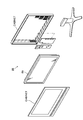
- FIG. 3 is an exploded perspective view of an LED module.
- FIG. 3 is an exploded cross-sectional view of the LED module (note that the cross-sectional direction is the direction of arrow A-A ′ in FIG. 1). These are the exploded top views of a LED module. These are side views of an LED module. These are the image images which show the light radiate
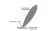
- FIG. 2 is a schematic perspective view of a simulation apparatus. These are images showing the illuminance distribution of light (Gaussian scattered light) emitted through two lenses. These are explanatory drawings explaining Gaussian scattering. These are explanatory drawings explaining Lambert scattering. These are the graphs which measured the Lambertian scattered light.
- FIG. 3 is an exploded perspective view of a liquid crystal display device. These are the exploded perspective views of the liquid crystal television which mounts a liquid crystal display device.
- FIG. 5 is an exploded perspective view of a conventional backlight unit. These are the image images which show the light radiate
- FIG. 17 shows a liquid crystal television 89 equipped with a liquid crystal display device (display device) 69.
- a liquid crystal television 89 can be said to be a television receiver because it receives a television broadcast signal and projects an image.
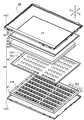
- FIG. 16 is an exploded perspective view showing a liquid crystal display device (display device) 69.
- the liquid crystal display device 69 includes a liquid crystal display panel (display panel) 59, a backlight unit (illumination device) 49 that supplies light to the liquid crystal display panel 59, and a housing HG that sandwiches them. (Front housing HG1 and back housing HG2).
- an active matrix substrate 51 including a switching element such as a TFT (Thin Film Transistor) and a counter substrate 52 facing the active matrix substrate 51 are bonded together with a sealant (not shown). Then, liquid crystal (not shown) is injected into the gap between the substrates 51 and 52.
- a switching element such as a TFT (Thin Film Transistor)
- a counter substrate 52 facing the active matrix substrate 51 are bonded together with a sealant (not shown). Then, liquid crystal (not shown) is injected into the gap between the substrates 51 and 52.
- a polarizing film 53 is attached to the light receiving surface side of the active matrix substrate 51 and the emission side of the counter substrate 52.
- the liquid crystal display panel 59 as described above displays an image using the change in transmittance caused by the inclination of the liquid crystal molecules.
- the backlight unit 49 includes an LED module (light emitting module) MJ, a backlight chassis 41, a large reflective sheet 42, a diffusion plate 43, a prism sheet 44, and a microlens sheet 45.
- LED module light emitting module
- the backlight unit 49 includes an LED module (light emitting module) MJ, a backlight chassis 41, a large reflective sheet 42, a diffusion plate 43, a prism sheet 44, and a microlens sheet 45.
- FIGS. 1 to 4 are shown in FIGS. 1 to 4 in addition to FIG. 1 is a partial perspective view of FIG. 16, and FIG. 2 is a cross-sectional view taken along the line A-A 'of FIG. 3 is an exploded plan view illustrating various members shown in FIG. 1, and FIG. 4 is a side view of FIG.
- a built-in reflective sheet 11 to be described later may be illustrated by a one-dot chain line, and a member positioned at the end of the broken line arrow covers a member on the root side of the broken line arrow.
- a built-in reflection sheet 11 and a large-format reflection sheet 42 described later are omitted for convenience.
- the LED module MJ includes a mounting substrate 21, an LED (Light Emitting Diode) 22, a lens 24, and a built-in reflection sheet (first reflection sheet) 11.
- the mounting substrate 21 is a plate-shaped and rectangular substrate, and a plurality of electrodes (not shown) are arranged on the mounting surface 21U. And LED22 which is a light emitting element is attached on these electrodes.
- a resist film (not shown) serving as a protective film is formed on the mounting surface 21U of the mounting substrate 21.
- the resist film is not particularly limited, but is desirably white having reflectivity. This is because even if light is incident on the resist film, the light is reflected by the resist film and tends to go outside, thereby eliminating the cause of unevenness in the amount of light due to light absorption by the mounting substrate 21.
- the LED 22 is a light source and emits light by a current through the electrodes of the mounting substrate 21. And there are many kinds of LED22, and the following LED22 is mentioned.
- the LED 22 includes a blue light emitting LED chip (light emitting chip) and a phosphor that receives light from the LED chip and fluoresces yellow light (the number of LED chips is the same). Not particularly limited).
- Such an LED 22 generates white light by the light from the LED chip emitting blue light and the light emitting fluorescence.
- the phosphor incorporated in the LED 22 is not limited to a phosphor that emits yellow light.
- the LED 22 includes a blue light emitting LED chip and a fluorescent material that receives light from the LED chip and emits green light and red light, and emits blue light and fluorescent light emitted from the LED chip ( White light may be generated with green light and red light.
- the LED chip built in the LED 22 is not limited to a blue light emitting device.
- the LED 22 may include a red LED chip that emits red light, a blue LED chip that emits blue light, and a phosphor that emits green light by receiving light from the blue LED chip. This is because such an LED 22 can generate white light from red light from the red LED chip, blue light from the blue LED chip, and green light that emits fluorescence.
- the LED 22 may not include any phosphor.
- the LED 22 may include a red LED chip that emits red light, a green LED chip that emits green light, and a blue LED chip that emits blue light, and generates white light using light from all the LED chips.
- a relatively long mounting board 21 mounted in a row is mounted.
- the two types of mounting boards 21 are arranged such that a row of five LEDs 22 and a row of eight LEDs 22 are arranged to form a row of 13 LEDs 22, and further, with respect to the direction in which the 13 LEDs 22 are arranged.
- the two types of mounting boards 21 are also arranged in the crossing (orthogonal) direction.
- the LEDs 22 are arranged in a matrix and emits planar light (for convenience, the direction in which different types of mounting boards 21 are arranged is defined as the X direction, and the direction in which the same type of mounting boards 21 are arranged is defined as the Y direction.
- the direction intersecting with the Z direction is defined as Z).
- the thirteen LEDs 22 arranged in the X direction are electrically connected in series, and the thirteen LEDs 22 connected in series are connected to another thirteen LEDs 22 connected in series along the Y direction. Electrically connected in parallel.
- the LEDs 22 arranged in a matrix are driven in parallel.
- the built-in reflective sheet 11 is a sheet having a reflective surface (built-in reflective surface) 11U, and is attached with the back surface of the reflective surface 11U facing the mounting surface 21U of the mounting board 21 (for details on the built-in reflective surface 11U). Will be described later). Since the built-in reflective sheet 11 includes the LED opening 11HL for exposing the LED 22 to the built-in reflective surface 11U, light from the LED 22 is not blocked.
- the built-in reflection sheet 11 includes a leg opening 11HF for allowing a leg 24F of the lens 24 to be described later to pass therethrough so as not to hinder the connection between the lens 24 covering the lens and the mounting substrate 21. That is, the built-in reflective sheet 11 is covered with the lens 24 and thus interposed between the lens 24 and the mounting substrate 21.
- the built-in reflection sheet 11 prevents the mounting surface 21U of the mounting substrate 21 from being exposed through the passage opening 42H for allowing the lens 24 formed on the large-format reflection sheet 42 to pass therethrough.
- the large reflective sheet 42 includes a passage opening 42H that is larger than the outer diameter of the lens 24 in order to expose the lens 24 to its own large reflective surface 42U. Then, when the lens 24 is exposed on the large reflective surface 42U of the large reflective sheet 42, a gap is generated between the outer edge 24E of the lens 24 and the inner edge of the passage opening 42H, and the mounting surface 21U of the mounting substrate 21 is formed from the gap. May be exposed. Therefore, the built-in reflection sheet 11 has a shape that borders the outer edge 24E of the lens 24 (an outer shape that surrounds the outer edge 24E), for example, a circle as shown in FIG.
- the lens 24 overlaps the built-in reflective surface 11U of the built-in reflective sheet 11, receives light from the LED 22, and transmits (emits) the light. More specifically, as shown in FIG. 2, the lens 24 has an accommodation recess DH that can accommodate the LED 22 on the back surface 24B (light receiving surface) side of the lens surface 24S, and aligns the position of the accommodation recess DH and the LED 22. The LED 22 exposed from the built-in reflection sheet 11 is covered. Then, the LED 22 is embedded in the lens 24, and the light from the LED 22 is reliably supplied into the lens 24. And most of the supplied light is emitted to the outside through the lens surface 24S.
- the lens surface 24S includes a recessed hole 24D in which a part of the lens surface 24S that overlaps the housing recess DH (that is, the LED 22) is recessed, as shown in FIGS. 1 to 4, for example.
- a curved surface divided by the depression hole 24D is generated on the lens surface 24S, and the light passing through the lens surface 24S is compared to the light passing through the lens surface without any depression hole, Do not concentrate light with relatively strong light intensity at one point.
- the lens 24 can be said to be a diffusing lens.
- the light from the LED 22 covered by the depression hole 24D is guided in a radial direction around the depression hole 24D by the lens surface 24S surrounding the depression hole 24D (see the image image in FIG. 5).
- the material for the lens 24 is not particularly limited, and examples thereof include acrylic resin (an acrylic resin having a refractive index nd of 1.49 to 1.50).
- the attachment of the lens 24 and the mounting substrate 21 is not particularly limited.
- a leg portion 24F that protrudes away from the lens surface 24S is formed on the outer edge 24E of the lens 24, and the mounting surface 21U and the leg portion 24F are, for example, an adhesive (not shown).
- the built-in reflective sheet 11 interposed between the lens 24 and the mounting substrate 21 has a leg opening 11HF through which the leg 24F passes).
- the backlight chassis 41 is, for example, a box-shaped member, and houses the plurality of LED modules MJ by spreading the LED modules MJ on the bottom surface 41B.
- the bottom surface 41B of the backlight chassis 41 and the mounting substrate 21 of the LED module MJ are connected via a rivet (not shown).
- Support pins for supporting the diffusion plate 43, the prism sheet 44, and the microlens sheet 45 may be attached to the bottom surface 41B of the backlight chassis 41. Then, the diffusion plate 43, the prism sheet 44, and the microlens sheet 45 may be stacked and supported in this order).
- the large reflective sheet (second reflective sheet) 42 is an optical sheet having a reflective surface 42U, and covers a plurality of LED modules MJ arranged in a matrix with the back surface of the reflective surface 42U facing.
- the large reflective sheet 42 includes a through hole 42H that is aligned with the position of the lens 24 of the LED module MJ, and exposes the lens 24 from the reflective surface 42U (note that the above-described rivets and support pins are not exposed). There should be holes).
- the lens 24 travels toward the bottom surface 41B side of the backlight chassis 41, it is reflected by the reflective surface 42U of the large-sized reflective sheet 42 and travels away from the bottom surface 41B. To do. Accordingly, the presence of the large reflective sheet 42 causes the light of the LED 22 to travel toward the diffusion plate 43 facing the reflective surface 42U without loss.
- the diffusion plate 43 is an optical sheet that overlaps the large reflective sheet 42, and diffuses the light emitted from the LED module MJ and the reflected light from the large reflective sheet 42U. That is, the diffusing plate 43 diffuses the planar light formed by the plurality of LED modules MJ and spreads the light over the entire liquid crystal display panel 59.
- the diffusion plate 43 preferably has a transmittance of 52% or more and 60% or less. This is because such a diffusing plate 43 can diffuse while appropriately transmitting light and suppress unevenness in the amount of light.
- the prism sheet 44 is an optical sheet that overlaps the diffusion plate 43.
- the prism sheet 44 arranges, for example, triangular prisms extending in one direction (linear) in a direction intersecting with one direction in the sheet surface. Thereby, the prism sheet 44 deflects the radiation characteristic of the light from the diffusion plate 43.
- the prisms extend along the Y direction with a small number of LEDs 22 arranged, and are arranged along the X direction with a large number of LEDs 22 arranged.
- the microlens sheet 45 is an optical sheet that overlaps the prism sheet 44.
- the microlens sheet 45 disperses the fine particles that refract and scatter light inside. As a result, the microlens sheet 45 suppresses the light / dark difference (light intensity unevenness) without locally condensing the light from the prism sheet 44.
- the backlight unit 49 as described above supplies the planar light formed by the plurality of LED modules MJ through the plurality of optical sheets 43 to 45 to the liquid crystal display panel 59.
- the non-light-emitting liquid crystal display panel 59 receives the light (backlight light) from the backlight unit 49 and improves the display function.
- FIG. 6 is a schematic diagram of the simulation device 79.
- This simulation device 79 includes an experimental unit 71 and a photographing camera 73.
- the experimental unit 71 has an LED module MJ that includes two lenses 24 in a box 72 that includes an opening and a reflecting surface that has a reflectance of about 97% on the bottom surface and a reflecting surface that has a reflectance of approximately 100% on the inner wall. Is installed. Furthermore, the experiment unit 71 arranges the diffusion plate 43 in the opening of the box 72, thereby allowing the light from the LED module MJ to pass through the diffusion plate 43.
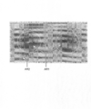
- the photographing camera 73 measures the illuminance on the surface of the diffusion plate 43 by photographing the diffusion plate 43. Specifically, as shown in FIG. 7, an image that can identify the illuminance level for each area in two dimensions is taken.
- an image showing two circles is obtained by the photographing camera 73.
- This circular image represents the light that has passed through the lens 24.
- a circular line shows the boundary line of the illumination intensity range with a height difference.
- the image in FIG. 7 includes an area AR1 surrounded only by a dotted line, and an area AR2 other than that (area surrounded by a one-dot chain line frame excluding the dotted line area) AR2.
- the LED module MJ showing the illuminance image as shown in FIG. 7 includes an LED 22, a mounting substrate 21 on which the LED 22 is mounted, a lens 24 for emitting light from the LED 22 from the lens surface 24S, and a mounting substrate from the back surface 24B of the lens surface 24S. And a built-in reflection sheet 11 having a built-in reflection surface 11U facing the back surface 24B of the lens surface 24S.
- Gaussian scattering as shown in FIG. 8 occurs in the built-in reflective surface 11U of the built-in reflective sheet 11.
- the light reflected by the back surface 24B of the lens 24 is further reflected by the built-in reflective surface 11U, reaches the back surface 24B of the lens 24, and enters the inside of the lens 24.
- the light reflected by the back surface 24B of the lens 24 is not absorbed by, for example, the mounting surface 21U or reflected by the mounting surface 21U and does not enter the back surface 24B of the lens 24. . That is, the light from the LED 22 is emitted through the lens 24 without loss.
- the area AR1 indicating the illuminance LN1 increases, and the illuminance of the entire illuminance range by the LED module MJ increases (in addition, FIG. 20 is given as an example of low illuminance of the entire illuminance range). .
- the light emitted from the LED module MJ is less likely to include light amount unevenness.
- the illuminance of the backlight unit 49 on which such an LED module MJ is mounted is also increased, and as a result, the light of the backlight unit 49 is less likely to include unevenness in the amount of light.
- the image quality of the liquid crystal display device 69 equipped with such a backlight unit 49 is also improved (in short, the liquid crystal display device 69 can display an image that does not include unevenness in the amount of light).
- the reflection that occurs on the built-in reflective surface 11U of the built-in reflective sheet 11 can be considered other than Gaussian scattering.
- the built-in reflective surface 11U may be subjected to texture processing to cause Lambertian scattering of light (in short, the built-in reflective surface 11U may be a completely diffuse reflective surface).
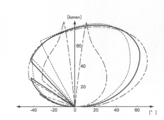
- FIG. 10 is a measurement result of a light distribution measurement system ⁇ Spectral Discoloration Color Difference Meter GC5000 manufactured by Nippon Denshoku Industries Co., Ltd. ⁇ .
- FIG. 10 is a polar coordinate graph, in which the horizontal axis is an angle [unit; °], and the normal direction size (vertical axis) is an illuminance [unit: lumen].
- the shape surrounded by the graph line indicates the reflection state of the light reflected at the incident point. Then, it can be seen from FIG. 10 that in the case of Lambert scattering, light is reflected (scattered) in various directions.
- the area AR1 indicating the illuminance LN1 is increased compared to the illuminance image of FIG.
- the illuminance of the entire illuminance range by MJ is further increased.
- the number of optical sheets for preventing unevenness in the amount of light included in the backlight unit 49 may be reduced (in short, the backlight unit 49 Cost and the backlight unit 49 also becomes thin).
- the built-in reflective surface 11U for Lambertian scattering includes a texture pattern
- the method of forming the texture pattern is not particularly limited.
- the embossed pattern may be formed by various methods such as masking, roll transfer, or extrusion.
- beads that scatter light may be coated on the built-in reflective surface 11U. That is, even if the built-in reflective surface 11U is a coated surface coated with beads, it is sufficient to cause Lambert scattering.
- the surface roughness [Ra] of the built-in reflective surface 11U having such a rough surface is 400 nm or more.
- a rough surface formed by embossing or the like may be formed on the back surface 24B of the lens 24. In this case, the light incident directly on the back surface 24B of the lens 24 is scattered from the LED 22.
- the built-in reflective surface 11U of the built-in reflective sheet 11 may be a Lambertian scattering surface or a Gaussian scattering surface.
- another part of the light diffused in various directions proceeds as shown in the optical path diagram of FIG. That is, a part of the light that has reached the back surface 24B of the lens 24 (a dashed-dotted arrow) enters the lens 24 as it is while being scattered.
- the light of the LED 22 is reliably emitted through the lens 24 without loss, and the illuminance of the entire illuminance range by the LED module MJ is further increased.
- Such a scattering state has been confirmed as a relatively good result by verification using, for example, optical analysis software SPEOS manufactured by OPTIS ⁇ Asia & Pacific.
- the large reflective sheet 42 has a reflectance of 97% or more.
- the luminance in the vicinity immediately above the lens 24 corresponds to the luminance in the vicinity immediately above the lens 24. Compared to, it will not be too low.
- the luminance curve Lp indicates the luminance of light from the LED module MJ covered by the large-format reflection sheet 42 having a reflectance of 97%.
- the luminance curve Lc indicates the luminance of light from the LED module MJ when the large-format reflection sheet 42 is not covered (note that the maximum luminance in the luminance curves Lp and Lc is approximately the same).
- the difference between the luminance near the lens 24 in the luminance curve Lp and the luminance near the lens 24 between the lenses 24 is the lens on the luminance curve Lc. This is smaller than the difference between the luminance in the vicinity immediately above 24 and the luminance in the vicinity immediately above between the lenses 24.
- the magnitude of the luminance difference indicates whether or not the light from the backlight unit 49 includes light amount unevenness (in short, the light amount unevenness occurs when the luminance difference is large). Then, the light from the backlight unit 49 on which the LED module MJ when not covering the large-format reflection sheet 42 includes light amount unevenness, but the LED covered with the large-format reflection sheet 42 having a reflectivity of 97%. The light from the backlight unit 49 on which the module MJ is mounted does not include light amount unevenness. That is, it can be said that it is desirable that the large-size reflection sheet 42 having a reflectance of 97% is mounted on the backlight unit 49.
- the shape (outer shape) of the built-in reflective sheet 11 is not limited to a circle as shown in FIG.
- the internal reflection sheet 11 having a rectangular outer shape may be used.
- the built-in reflective sheet 11 may have a substantially rectangular outer shape and include a slit ST for avoiding contact between the LED 22 and the lens leg 24F.
- the built-in reflective sheet 11 shown in FIG. 15 has three cuts ST on one side of the rectangular outer shape. And, one notch ST1 at the center of the three parallel parts sandwiches the LED 22 and one leg 24F of the lens 24, and the remaining two notches ST2 and ST3 are each one. Designed to sandwich the leg 24F.
- the built-in reflection sheet 11 After the lens 24 is attached to the mounting substrate 21, the built-in reflection sheet 11 is moved along the mounting surface 21U, so that the mounting surface 21U and the back surface 24B of the lens 24 are obtained.
- the built-in reflection sheet 11 fits between the two. Therefore, the degree of freedom in assembling the LED module MJ increases. Further, the built-in reflective sheet 11 can be removed from the LED module MJ once completed (rework becomes possible).
- the light guide plate is omitted, and the LED directly enters the optical sheet (such as a diffusion plate).
- the optical sheet such as a diffusion plate.
- the distance from the LED to the diffusion plate should be long.
- the lens 24 including the lens surface 24S having the recessed hole 24D covers each LED 22, the light from the LED 22 is sufficiently diffused before reaching the diffusion plate 43.
- Backlight does not include unevenness in the amount of light.
- the distance between the LED 22 and the diffusion plate 43 may be relatively short (in short, the backlight unit 49 is relatively thin, and the liquid crystal display device 69 on which the backlight unit 49 is mounted is also likely to be thin).
- the driving heat of the LED 22 tends to be confined in a narrow space called the accommodation recess DH of the lens 24 (and the LED 22 cannot maintain a relatively high light intensity due to its own driving heat).
- the LED module MJ is attached to the backlight chassis 41 formed of a material with high heat dissipation, for example, metal.
- a separate heat dissipation member is not required between the mounting substrate 21 and the bottom surface 41B of the backlight chassis 41.
- the backlight unit 49 capable of maintaining the light intensity over a long period of time at a low cost is completed.
- the LED 22 which is a light emitting element is used as the light source.
- the present invention is not limited to this.
- it may be a light emitting element formed of a self-luminous material such as organic EL (Electro-Luminescence) or inorganic EL.
Landscapes
- Physics & Mathematics (AREA)
- Nonlinear Science (AREA)
- General Physics & Mathematics (AREA)
- Optics & Photonics (AREA)
- Mathematical Physics (AREA)
- Chemical & Material Sciences (AREA)
- Crystallography & Structural Chemistry (AREA)
- Planar Illumination Modules (AREA)
Abstract
Priority Applications (2)
| Application Number | Priority Date | Filing Date | Title |
|---|---|---|---|
| US13/376,395 US20120081614A1 (en) | 2009-06-15 | 2010-03-15 | Light-emitting module, illumination device, display device, and television receiver |
| CN2010800264245A CN102460746A (zh) | 2009-06-15 | 2010-03-15 | 发光模块、照明装置、显示装置以及电视接收装置 |
Applications Claiming Priority (2)
| Application Number | Priority Date | Filing Date | Title |
|---|---|---|---|
| JP2009-141919 | 2009-06-15 | ||
| JP2009141919 | 2009-06-15 |
Publications (1)
| Publication Number | Publication Date |
|---|---|
| WO2010146904A1 true WO2010146904A1 (fr) | 2010-12-23 |
Family
ID=43356234
Family Applications (1)
| Application Number | Title | Priority Date | Filing Date |
|---|---|---|---|
| PCT/JP2010/054306 Ceased WO2010146904A1 (fr) | 2009-06-15 | 2010-03-15 | Module electroluminescent, dispositif d'eclairage, dispositif d'affichage, et recepteur de television |
Country Status (3)
| Country | Link |
|---|---|
| US (1) | US20120081614A1 (fr) |
| CN (1) | CN102460746A (fr) |
| WO (1) | WO2010146904A1 (fr) |
Cited By (6)
| Publication number | Priority date | Publication date | Assignee | Title |
|---|---|---|---|---|
| JP2012004078A (ja) * | 2010-06-21 | 2012-01-05 | Enplas Corp | 発光装置、面光源装置、表示装置及び光束制御部材 |
| EP2584395A1 (fr) * | 2011-10-21 | 2013-04-24 | Barco N.V. | Systèmes d'émission de lumière |
| JP2013143219A (ja) * | 2012-01-10 | 2013-07-22 | Sharp Corp | 照明装置、表示装置及びテレビ受信装置 |
| JP2013143220A (ja) * | 2012-01-10 | 2013-07-22 | Sharp Corp | 照明装置、表示装置、及びテレビ受信装置 |
| JP2015002066A (ja) * | 2013-06-14 | 2015-01-05 | 岩崎電気株式会社 | 光学レンズユニット及び照明器具 |
| JPWO2018181701A1 (ja) * | 2017-03-31 | 2019-04-04 | 株式会社Ctnb | 配光制御素子、配光調整手段、反射部材、補強板、照明ユニット、ディスプレイ及びテレビ受信機 |
Families Citing this family (7)
| Publication number | Priority date | Publication date | Assignee | Title |
|---|---|---|---|---|
| WO2014031877A2 (fr) | 2012-08-22 | 2014-02-27 | Seoul Semiconductor Co., Ltd. | Lentille d'éclairage pour rétroéclairages à led |
| US10503010B2 (en) | 2012-08-22 | 2019-12-10 | Seoul Semiconductor Co., Ltd. | Thin direct-view LED backlights |
| US9523884B2 (en) * | 2014-06-24 | 2016-12-20 | Shenzhen China Star Optoelectronics Technology Co., Ltd | Direct type backlight module unit of dual-side liquid crystal display device |
| US20160004123A1 (en) * | 2014-07-02 | 2016-01-07 | Kabushiki Kaisha Toshiba | Image display apparatus |
| CN107452849B (zh) * | 2016-06-01 | 2019-08-27 | 光宝光电(常州)有限公司 | 发光二极管封装结构 |
| US10153416B1 (en) * | 2017-05-23 | 2018-12-11 | Radiant Choice Limited | Package body and light emitting device using same |
| JP7281363B2 (ja) * | 2019-08-10 | 2023-05-25 | Hoya株式会社 | 光照射装置 |
Citations (5)
| Publication number | Priority date | Publication date | Assignee | Title |
|---|---|---|---|---|
| JP2006228698A (ja) * | 2005-02-18 | 2006-08-31 | Samsung Electro-Mechanics Co Ltd | 導光機能を有する直下型バックライト装置 |
| JP2008147147A (ja) * | 2006-12-13 | 2008-06-26 | Sony Corp | バックライト装置及び液晶表示装置 |
| JP2008258146A (ja) * | 2007-04-04 | 2008-10-23 | Ctx Opto Electronics Corp | 高輝度拡散板 |
| JP2009044016A (ja) * | 2007-08-09 | 2009-02-26 | Sharp Corp | 発光装置およびこれを備える照明装置 |
| JP2009117207A (ja) * | 2007-11-07 | 2009-05-28 | Enplas Corp | 発光装置、面光源装置、及び表示装置 |
Family Cites Families (2)
| Publication number | Priority date | Publication date | Assignee | Title |
|---|---|---|---|---|
| US4714983A (en) * | 1985-06-10 | 1987-12-22 | Motorola, Inc. | Uniform emission backlight |
| KR100674850B1 (ko) * | 2005-05-02 | 2007-01-26 | 삼성전기주식회사 | 하이브리드 백라이트 장치 |
-
2010
- 2010-03-15 CN CN2010800264245A patent/CN102460746A/zh active Pending
- 2010-03-15 US US13/376,395 patent/US20120081614A1/en not_active Abandoned
- 2010-03-15 WO PCT/JP2010/054306 patent/WO2010146904A1/fr not_active Ceased
Patent Citations (5)
| Publication number | Priority date | Publication date | Assignee | Title |
|---|---|---|---|---|
| JP2006228698A (ja) * | 2005-02-18 | 2006-08-31 | Samsung Electro-Mechanics Co Ltd | 導光機能を有する直下型バックライト装置 |
| JP2008147147A (ja) * | 2006-12-13 | 2008-06-26 | Sony Corp | バックライト装置及び液晶表示装置 |
| JP2008258146A (ja) * | 2007-04-04 | 2008-10-23 | Ctx Opto Electronics Corp | 高輝度拡散板 |
| JP2009044016A (ja) * | 2007-08-09 | 2009-02-26 | Sharp Corp | 発光装置およびこれを備える照明装置 |
| JP2009117207A (ja) * | 2007-11-07 | 2009-05-28 | Enplas Corp | 発光装置、面光源装置、及び表示装置 |
Cited By (7)
| Publication number | Priority date | Publication date | Assignee | Title |
|---|---|---|---|---|
| JP2012004078A (ja) * | 2010-06-21 | 2012-01-05 | Enplas Corp | 発光装置、面光源装置、表示装置及び光束制御部材 |
| EP2584395A1 (fr) * | 2011-10-21 | 2013-04-24 | Barco N.V. | Systèmes d'émission de lumière |
| US8842705B2 (en) | 2011-10-21 | 2014-09-23 | Barco N.V. | Light emitting systems |
| JP2013143219A (ja) * | 2012-01-10 | 2013-07-22 | Sharp Corp | 照明装置、表示装置及びテレビ受信装置 |
| JP2013143220A (ja) * | 2012-01-10 | 2013-07-22 | Sharp Corp | 照明装置、表示装置、及びテレビ受信装置 |
| JP2015002066A (ja) * | 2013-06-14 | 2015-01-05 | 岩崎電気株式会社 | 光学レンズユニット及び照明器具 |
| JPWO2018181701A1 (ja) * | 2017-03-31 | 2019-04-04 | 株式会社Ctnb | 配光制御素子、配光調整手段、反射部材、補強板、照明ユニット、ディスプレイ及びテレビ受信機 |
Also Published As
| Publication number | Publication date |
|---|---|
| US20120081614A1 (en) | 2012-04-05 |
| CN102460746A (zh) | 2012-05-16 |
Similar Documents
| Publication | Publication Date | Title |
|---|---|---|
| WO2010146904A1 (fr) | Module electroluminescent, dispositif d'eclairage, dispositif d'affichage, et recepteur de television | |
| JP5228109B2 (ja) | レンズユニット、発光モジュール、照明装置、表示装置、およびテレビ受像装置 | |
| WO2010146905A1 (fr) | Module electroluminescent, dispositif d'eclairage, dispositif d'affichage, et dispositif recepteur de television | |
| US7637646B2 (en) | Backlight assembly and liquid crystal display device having the same | |
| TWI466319B (zh) | A light emitting device, a lighting device, and a display device | |
| TWI467118B (zh) | A light emitting device, a lighting device, and a display device | |
| US8430519B2 (en) | Lighting device, display device and television receiver | |
| US7862221B2 (en) | Optical lens, optical package having the same, backlight assembly having the same and display device having the same | |
| EP2515027A1 (fr) | Dispositif d'éclairage, dispositif d'affichage et récepteur de télévision | |
| EP2458263A1 (fr) | Picot de support, dispositif d éclairage, dispositif d affichage, et dispositif de réception de télévision | |
| WO2010146903A1 (fr) | Module émetteur de lumière, dispositif d'éclairage, dispositif d'affichage et dispositif récepteur de télévision | |
| WO2011016269A1 (fr) | Lentille, module électroluminescent, boîtier déléments électroluminescents, dispositif déclairage, dispositif daffichage et récepteur de télévision | |
| US10352530B2 (en) | Lens, light emitting apparatus including the lens, and backlight unit including the apparatus | |
| TWM565322U (zh) | Direct type backlight module and display device | |
| WO2010146902A1 (fr) | Module émetteur de lumière, dispositif d'éclairage, dispositif d'affichage et dispositif récepteur de télévision | |
| KR20140089058A (ko) | 백라이트 장치 | |
| JP2013218940A (ja) | 発光モジュール、それを備えた照明装置および表示装置 | |
| US9720161B2 (en) | LCD backlight device having light guide plate with optical scattering dots | |
| WO2011004642A1 (fr) | Lentille, conditionnement d'élément électroluminescent, module électroluminescent, dispositif d'éclairage, dispositif d'affichage et télévision | |
| US8657458B2 (en) | Lighting device, display device and television receiver | |
| JP2009043738A (ja) | 面状光源装置 | |
| EP2762959B1 (fr) | Appareil d'affichage | |
| WO2012026164A1 (fr) | Dispositif d'éclairage, dispositif d'affichage | |
| US20090147533A1 (en) | Display Device | |
| WO2011102335A1 (fr) | Ensemble d'éclairage, dispositif d'éclairage et dispositif d'affichage |
Legal Events
| Date | Code | Title | Description |
|---|---|---|---|
| WWE | Wipo information: entry into national phase |
Ref document number: 201080026424.5 Country of ref document: CN |
|
| 121 | Ep: the epo has been informed by wipo that ep was designated in this application |
Ref document number: 10789281 Country of ref document: EP Kind code of ref document: A1 |
|
| WWE | Wipo information: entry into national phase |
Ref document number: 13376395 Country of ref document: US |
|
| NENP | Non-entry into the national phase |
Ref country code: DE |
|
| 122 | Ep: pct application non-entry in european phase |
Ref document number: 10789281 Country of ref document: EP Kind code of ref document: A1 |
|
| NENP | Non-entry into the national phase |
Ref country code: JP |