WO2010146967A1 - Laminated ceramic electronic component and manufacturing method therefor - Google Patents
Laminated ceramic electronic component and manufacturing method therefor Download PDFInfo
- Publication number
- WO2010146967A1 WO2010146967A1 PCT/JP2010/058618 JP2010058618W WO2010146967A1 WO 2010146967 A1 WO2010146967 A1 WO 2010146967A1 JP 2010058618 W JP2010058618 W JP 2010058618W WO 2010146967 A1 WO2010146967 A1 WO 2010146967A1
- Authority
- WO
- WIPO (PCT)
- Prior art keywords
- ceramic
- laminate
- temperature
- grain region
- internal electrode
- Prior art date
- Legal status (The legal status is an assumption and is not a legal conclusion. Google has not performed a legal analysis and makes no representation as to the accuracy of the status listed.)
- Ceased
Links
Images





Classifications
-
- B—PERFORMING OPERATIONS; TRANSPORTING
- B32—LAYERED PRODUCTS
- B32B—LAYERED PRODUCTS, i.e. PRODUCTS BUILT-UP OF STRATA OF FLAT OR NON-FLAT, e.g. CELLULAR OR HONEYCOMB, FORM
- B32B18/00—Layered products essentially comprising ceramics, e.g. refractory products
-
- H—ELECTRICITY
- H01—ELECTRIC ELEMENTS
- H01G—CAPACITORS; CAPACITORS, RECTIFIERS, DETECTORS, SWITCHING DEVICES, LIGHT-SENSITIVE OR TEMPERATURE-SENSITIVE DEVICES OF THE ELECTROLYTIC TYPE
- H01G4/00—Fixed capacitors; Processes of their manufacture
- H01G4/002—Details
- H01G4/005—Electrodes
-
- C—CHEMISTRY; METALLURGY
- C04—CEMENTS; CONCRETE; ARTIFICIAL STONE; CERAMICS; REFRACTORIES
- C04B—LIME, MAGNESIA; SLAG; CEMENTS; COMPOSITIONS THEREOF, e.g. MORTARS, CONCRETE OR LIKE BUILDING MATERIALS; ARTIFICIAL STONE; CERAMICS; REFRACTORIES; TREATMENT OF NATURAL STONE
- C04B35/00—Shaped ceramic products characterised by their composition; Ceramics compositions; Processing powders of inorganic compounds preparatory to the manufacturing of ceramic products
- C04B35/01—Shaped ceramic products characterised by their composition; Ceramics compositions; Processing powders of inorganic compounds preparatory to the manufacturing of ceramic products based on oxide ceramics
- C04B35/46—Shaped ceramic products characterised by their composition; Ceramics compositions; Processing powders of inorganic compounds preparatory to the manufacturing of ceramic products based on oxide ceramics based on titanium oxides or titanates
- C04B35/462—Shaped ceramic products characterised by their composition; Ceramics compositions; Processing powders of inorganic compounds preparatory to the manufacturing of ceramic products based on oxide ceramics based on titanium oxides or titanates based on titanates
- C04B35/465—Shaped ceramic products characterised by their composition; Ceramics compositions; Processing powders of inorganic compounds preparatory to the manufacturing of ceramic products based on oxide ceramics based on titanium oxides or titanates based on titanates based on alkaline earth metal titanates
- C04B35/468—Shaped ceramic products characterised by their composition; Ceramics compositions; Processing powders of inorganic compounds preparatory to the manufacturing of ceramic products based on oxide ceramics based on titanium oxides or titanates based on titanates based on alkaline earth metal titanates based on barium titanates
- C04B35/4682—Shaped ceramic products characterised by their composition; Ceramics compositions; Processing powders of inorganic compounds preparatory to the manufacturing of ceramic products based on oxide ceramics based on titanium oxides or titanates based on titanates based on alkaline earth metal titanates based on barium titanates based on BaTiO3 perovskite phase
-
- C—CHEMISTRY; METALLURGY
- C04—CEMENTS; CONCRETE; ARTIFICIAL STONE; CERAMICS; REFRACTORIES
- C04B—LIME, MAGNESIA; SLAG; CEMENTS; COMPOSITIONS THEREOF, e.g. MORTARS, CONCRETE OR LIKE BUILDING MATERIALS; ARTIFICIAL STONE; CERAMICS; REFRACTORIES; TREATMENT OF NATURAL STONE
- C04B35/00—Shaped ceramic products characterised by their composition; Ceramics compositions; Processing powders of inorganic compounds preparatory to the manufacturing of ceramic products
- C04B35/622—Forming processes; Processing powders of inorganic compounds preparatory to the manufacturing of ceramic products
- C04B35/626—Preparing or treating the powders individually or as batches ; preparing or treating macroscopic reinforcing agents for ceramic products, e.g. fibres; mechanical aspects section B
- C04B35/62605—Treating the starting powders individually or as mixtures
- C04B35/62685—Treating the starting powders individually or as mixtures characterised by the order of addition of constituents or additives
-
- H—ELECTRICITY
- H01—ELECTRIC ELEMENTS
- H01G—CAPACITORS; CAPACITORS, RECTIFIERS, DETECTORS, SWITCHING DEVICES, LIGHT-SENSITIVE OR TEMPERATURE-SENSITIVE DEVICES OF THE ELECTROLYTIC TYPE
- H01G4/00—Fixed capacitors; Processes of their manufacture
- H01G4/002—Details
- H01G4/005—Electrodes
- H01G4/012—Form of non-self-supporting electrodes
-
- H—ELECTRICITY
- H01—ELECTRIC ELEMENTS
- H01G—CAPACITORS; CAPACITORS, RECTIFIERS, DETECTORS, SWITCHING DEVICES, LIGHT-SENSITIVE OR TEMPERATURE-SENSITIVE DEVICES OF THE ELECTROLYTIC TYPE
- H01G4/00—Fixed capacitors; Processes of their manufacture
- H01G4/002—Details
- H01G4/018—Dielectrics
- H01G4/06—Solid dielectrics
- H01G4/08—Inorganic dielectrics
- H01G4/12—Ceramic dielectrics
-
- H—ELECTRICITY
- H01—ELECTRIC ELEMENTS
- H01G—CAPACITORS; CAPACITORS, RECTIFIERS, DETECTORS, SWITCHING DEVICES, LIGHT-SENSITIVE OR TEMPERATURE-SENSITIVE DEVICES OF THE ELECTROLYTIC TYPE
- H01G4/00—Fixed capacitors; Processes of their manufacture
- H01G4/002—Details
- H01G4/018—Dielectrics
- H01G4/06—Solid dielectrics
- H01G4/08—Inorganic dielectrics
- H01G4/12—Ceramic dielectrics
- H01G4/1209—Ceramic dielectrics characterised by the ceramic dielectric material
-
- H—ELECTRICITY
- H01—ELECTRIC ELEMENTS
- H01G—CAPACITORS; CAPACITORS, RECTIFIERS, DETECTORS, SWITCHING DEVICES, LIGHT-SENSITIVE OR TEMPERATURE-SENSITIVE DEVICES OF THE ELECTROLYTIC TYPE
- H01G4/00—Fixed capacitors; Processes of their manufacture
- H01G4/30—Stacked capacitors
-
- C—CHEMISTRY; METALLURGY
- C04—CEMENTS; CONCRETE; ARTIFICIAL STONE; CERAMICS; REFRACTORIES
- C04B—LIME, MAGNESIA; SLAG; CEMENTS; COMPOSITIONS THEREOF, e.g. MORTARS, CONCRETE OR LIKE BUILDING MATERIALS; ARTIFICIAL STONE; CERAMICS; REFRACTORIES; TREATMENT OF NATURAL STONE
- C04B2235/00—Aspects relating to ceramic starting mixtures or sintered ceramic products
- C04B2235/02—Composition of constituents of the starting material or of secondary phases of the final product
- C04B2235/30—Constituents and secondary phases not being of a fibrous nature
- C04B2235/32—Metal oxides, mixed metal oxides, or oxide-forming salts thereof, e.g. carbonates, nitrates, (oxy)hydroxides, chlorides
- C04B2235/3205—Alkaline earth oxides or oxide forming salts thereof, e.g. beryllium oxide
- C04B2235/3206—Magnesium oxides or oxide-forming salts thereof
-
- C—CHEMISTRY; METALLURGY
- C04—CEMENTS; CONCRETE; ARTIFICIAL STONE; CERAMICS; REFRACTORIES
- C04B—LIME, MAGNESIA; SLAG; CEMENTS; COMPOSITIONS THEREOF, e.g. MORTARS, CONCRETE OR LIKE BUILDING MATERIALS; ARTIFICIAL STONE; CERAMICS; REFRACTORIES; TREATMENT OF NATURAL STONE
- C04B2235/00—Aspects relating to ceramic starting mixtures or sintered ceramic products
- C04B2235/02—Composition of constituents of the starting material or of secondary phases of the final product
- C04B2235/30—Constituents and secondary phases not being of a fibrous nature
- C04B2235/32—Metal oxides, mixed metal oxides, or oxide-forming salts thereof, e.g. carbonates, nitrates, (oxy)hydroxides, chlorides
- C04B2235/3205—Alkaline earth oxides or oxide forming salts thereof, e.g. beryllium oxide
- C04B2235/3215—Barium oxides or oxide-forming salts thereof
-
- C—CHEMISTRY; METALLURGY
- C04—CEMENTS; CONCRETE; ARTIFICIAL STONE; CERAMICS; REFRACTORIES
- C04B—LIME, MAGNESIA; SLAG; CEMENTS; COMPOSITIONS THEREOF, e.g. MORTARS, CONCRETE OR LIKE BUILDING MATERIALS; ARTIFICIAL STONE; CERAMICS; REFRACTORIES; TREATMENT OF NATURAL STONE
- C04B2235/00—Aspects relating to ceramic starting mixtures or sintered ceramic products
- C04B2235/02—Composition of constituents of the starting material or of secondary phases of the final product
- C04B2235/30—Constituents and secondary phases not being of a fibrous nature
- C04B2235/32—Metal oxides, mixed metal oxides, or oxide-forming salts thereof, e.g. carbonates, nitrates, (oxy)hydroxides, chlorides
- C04B2235/3224—Rare earth oxide or oxide forming salts thereof, e.g. scandium oxide
-
- C—CHEMISTRY; METALLURGY
- C04—CEMENTS; CONCRETE; ARTIFICIAL STONE; CERAMICS; REFRACTORIES
- C04B—LIME, MAGNESIA; SLAG; CEMENTS; COMPOSITIONS THEREOF, e.g. MORTARS, CONCRETE OR LIKE BUILDING MATERIALS; ARTIFICIAL STONE; CERAMICS; REFRACTORIES; TREATMENT OF NATURAL STONE
- C04B2235/00—Aspects relating to ceramic starting mixtures or sintered ceramic products
- C04B2235/02—Composition of constituents of the starting material or of secondary phases of the final product
- C04B2235/30—Constituents and secondary phases not being of a fibrous nature
- C04B2235/32—Metal oxides, mixed metal oxides, or oxide-forming salts thereof, e.g. carbonates, nitrates, (oxy)hydroxides, chlorides
- C04B2235/3231—Refractory metal oxides, their mixed metal oxides, or oxide-forming salts thereof
- C04B2235/3232—Titanium oxides or titanates, e.g. rutile or anatase
- C04B2235/3234—Titanates, not containing zirconia
- C04B2235/3236—Alkaline earth titanates
-
- C—CHEMISTRY; METALLURGY
- C04—CEMENTS; CONCRETE; ARTIFICIAL STONE; CERAMICS; REFRACTORIES
- C04B—LIME, MAGNESIA; SLAG; CEMENTS; COMPOSITIONS THEREOF, e.g. MORTARS, CONCRETE OR LIKE BUILDING MATERIALS; ARTIFICIAL STONE; CERAMICS; REFRACTORIES; TREATMENT OF NATURAL STONE
- C04B2235/00—Aspects relating to ceramic starting mixtures or sintered ceramic products
- C04B2235/02—Composition of constituents of the starting material or of secondary phases of the final product
- C04B2235/30—Constituents and secondary phases not being of a fibrous nature
- C04B2235/32—Metal oxides, mixed metal oxides, or oxide-forming salts thereof, e.g. carbonates, nitrates, (oxy)hydroxides, chlorides
- C04B2235/3262—Manganese oxides, manganates, rhenium oxides or oxide-forming salts thereof, e.g. MnO
-
- C—CHEMISTRY; METALLURGY
- C04—CEMENTS; CONCRETE; ARTIFICIAL STONE; CERAMICS; REFRACTORIES
- C04B—LIME, MAGNESIA; SLAG; CEMENTS; COMPOSITIONS THEREOF, e.g. MORTARS, CONCRETE OR LIKE BUILDING MATERIALS; ARTIFICIAL STONE; CERAMICS; REFRACTORIES; TREATMENT OF NATURAL STONE
- C04B2235/00—Aspects relating to ceramic starting mixtures or sintered ceramic products
- C04B2235/02—Composition of constituents of the starting material or of secondary phases of the final product
- C04B2235/30—Constituents and secondary phases not being of a fibrous nature
- C04B2235/34—Non-metal oxides, non-metal mixed oxides, or salts thereof that form the non-metal oxides upon heating, e.g. carbonates, nitrates, (oxy)hydroxides, chlorides
- C04B2235/3418—Silicon oxide, silicic acids or oxide forming salts thereof, e.g. silica sol, fused silica, silica fume, cristobalite, quartz or flint
-
- C—CHEMISTRY; METALLURGY
- C04—CEMENTS; CONCRETE; ARTIFICIAL STONE; CERAMICS; REFRACTORIES
- C04B—LIME, MAGNESIA; SLAG; CEMENTS; COMPOSITIONS THEREOF, e.g. MORTARS, CONCRETE OR LIKE BUILDING MATERIALS; ARTIFICIAL STONE; CERAMICS; REFRACTORIES; TREATMENT OF NATURAL STONE
- C04B2235/00—Aspects relating to ceramic starting mixtures or sintered ceramic products
- C04B2235/02—Composition of constituents of the starting material or of secondary phases of the final product
- C04B2235/50—Constituents or additives of the starting mixture chosen for their shape or used because of their shape or their physical appearance
- C04B2235/54—Particle size related information
- C04B2235/5418—Particle size related information expressed by the size of the particles or aggregates thereof
- C04B2235/5445—Particle size related information expressed by the size of the particles or aggregates thereof submicron sized, i.e. from 0,1 to 1 micron
-
- C—CHEMISTRY; METALLURGY
- C04—CEMENTS; CONCRETE; ARTIFICIAL STONE; CERAMICS; REFRACTORIES
- C04B—LIME, MAGNESIA; SLAG; CEMENTS; COMPOSITIONS THEREOF, e.g. MORTARS, CONCRETE OR LIKE BUILDING MATERIALS; ARTIFICIAL STONE; CERAMICS; REFRACTORIES; TREATMENT OF NATURAL STONE
- C04B2235/00—Aspects relating to ceramic starting mixtures or sintered ceramic products
- C04B2235/65—Aspects relating to heat treatments of ceramic bodies such as green ceramics or pre-sintered ceramics, e.g. burning, sintering or melting processes
- C04B2235/656—Aspects relating to heat treatments of ceramic bodies such as green ceramics or pre-sintered ceramics, e.g. burning, sintering or melting processes characterised by specific heating conditions during heat treatment
-
- C—CHEMISTRY; METALLURGY
- C04—CEMENTS; CONCRETE; ARTIFICIAL STONE; CERAMICS; REFRACTORIES
- C04B—LIME, MAGNESIA; SLAG; CEMENTS; COMPOSITIONS THEREOF, e.g. MORTARS, CONCRETE OR LIKE BUILDING MATERIALS; ARTIFICIAL STONE; CERAMICS; REFRACTORIES; TREATMENT OF NATURAL STONE
- C04B2235/00—Aspects relating to ceramic starting mixtures or sintered ceramic products
- C04B2235/65—Aspects relating to heat treatments of ceramic bodies such as green ceramics or pre-sintered ceramics, e.g. burning, sintering or melting processes
- C04B2235/656—Aspects relating to heat treatments of ceramic bodies such as green ceramics or pre-sintered ceramics, e.g. burning, sintering or melting processes characterised by specific heating conditions during heat treatment
- C04B2235/6562—Heating rate
-
- C—CHEMISTRY; METALLURGY
- C04—CEMENTS; CONCRETE; ARTIFICIAL STONE; CERAMICS; REFRACTORIES
- C04B—LIME, MAGNESIA; SLAG; CEMENTS; COMPOSITIONS THEREOF, e.g. MORTARS, CONCRETE OR LIKE BUILDING MATERIALS; ARTIFICIAL STONE; CERAMICS; REFRACTORIES; TREATMENT OF NATURAL STONE
- C04B2235/00—Aspects relating to ceramic starting mixtures or sintered ceramic products
- C04B2235/65—Aspects relating to heat treatments of ceramic bodies such as green ceramics or pre-sintered ceramics, e.g. burning, sintering or melting processes
- C04B2235/656—Aspects relating to heat treatments of ceramic bodies such as green ceramics or pre-sintered ceramics, e.g. burning, sintering or melting processes characterised by specific heating conditions during heat treatment
- C04B2235/6567—Treatment time
-
- C—CHEMISTRY; METALLURGY
- C04—CEMENTS; CONCRETE; ARTIFICIAL STONE; CERAMICS; REFRACTORIES
- C04B—LIME, MAGNESIA; SLAG; CEMENTS; COMPOSITIONS THEREOF, e.g. MORTARS, CONCRETE OR LIKE BUILDING MATERIALS; ARTIFICIAL STONE; CERAMICS; REFRACTORIES; TREATMENT OF NATURAL STONE
- C04B2235/00—Aspects relating to ceramic starting mixtures or sintered ceramic products
- C04B2235/65—Aspects relating to heat treatments of ceramic bodies such as green ceramics or pre-sintered ceramics, e.g. burning, sintering or melting processes
- C04B2235/658—Atmosphere during thermal treatment
- C04B2235/6582—Hydrogen containing atmosphere
-
- C—CHEMISTRY; METALLURGY
- C04—CEMENTS; CONCRETE; ARTIFICIAL STONE; CERAMICS; REFRACTORIES
- C04B—LIME, MAGNESIA; SLAG; CEMENTS; COMPOSITIONS THEREOF, e.g. MORTARS, CONCRETE OR LIKE BUILDING MATERIALS; ARTIFICIAL STONE; CERAMICS; REFRACTORIES; TREATMENT OF NATURAL STONE
- C04B2235/00—Aspects relating to ceramic starting mixtures or sintered ceramic products
- C04B2235/65—Aspects relating to heat treatments of ceramic bodies such as green ceramics or pre-sintered ceramics, e.g. burning, sintering or melting processes
- C04B2235/658—Atmosphere during thermal treatment
- C04B2235/6583—Oxygen containing atmosphere, e.g. with changing oxygen pressures
- C04B2235/6584—Oxygen containing atmosphere, e.g. with changing oxygen pressures at an oxygen percentage below that of air
-
- C—CHEMISTRY; METALLURGY
- C04—CEMENTS; CONCRETE; ARTIFICIAL STONE; CERAMICS; REFRACTORIES
- C04B—LIME, MAGNESIA; SLAG; CEMENTS; COMPOSITIONS THEREOF, e.g. MORTARS, CONCRETE OR LIKE BUILDING MATERIALS; ARTIFICIAL STONE; CERAMICS; REFRACTORIES; TREATMENT OF NATURAL STONE
- C04B2235/00—Aspects relating to ceramic starting mixtures or sintered ceramic products
- C04B2235/65—Aspects relating to heat treatments of ceramic bodies such as green ceramics or pre-sintered ceramics, e.g. burning, sintering or melting processes
- C04B2235/658—Atmosphere during thermal treatment
- C04B2235/6588—Water vapor containing atmospheres
-
- C—CHEMISTRY; METALLURGY
- C04—CEMENTS; CONCRETE; ARTIFICIAL STONE; CERAMICS; REFRACTORIES
- C04B—LIME, MAGNESIA; SLAG; CEMENTS; COMPOSITIONS THEREOF, e.g. MORTARS, CONCRETE OR LIKE BUILDING MATERIALS; ARTIFICIAL STONE; CERAMICS; REFRACTORIES; TREATMENT OF NATURAL STONE
- C04B2235/00—Aspects relating to ceramic starting mixtures or sintered ceramic products
- C04B2235/70—Aspects relating to sintered or melt-casted ceramic products
- C04B2235/72—Products characterised by the absence or the low content of specific components, e.g. alkali metal free alumina ceramics
- C04B2235/721—Carbon content
-
- C—CHEMISTRY; METALLURGY
- C04—CEMENTS; CONCRETE; ARTIFICIAL STONE; CERAMICS; REFRACTORIES
- C04B—LIME, MAGNESIA; SLAG; CEMENTS; COMPOSITIONS THEREOF, e.g. MORTARS, CONCRETE OR LIKE BUILDING MATERIALS; ARTIFICIAL STONE; CERAMICS; REFRACTORIES; TREATMENT OF NATURAL STONE
- C04B2235/00—Aspects relating to ceramic starting mixtures or sintered ceramic products
- C04B2235/70—Aspects relating to sintered or melt-casted ceramic products
- C04B2235/74—Physical characteristics
- C04B2235/78—Grain sizes and shapes, product microstructures, e.g. acicular grains, equiaxed grains, platelet-structures
- C04B2235/785—Submicron sized grains, i.e. from 0,1 to 1 micron
-
- C—CHEMISTRY; METALLURGY
- C04—CEMENTS; CONCRETE; ARTIFICIAL STONE; CERAMICS; REFRACTORIES
- C04B—LIME, MAGNESIA; SLAG; CEMENTS; COMPOSITIONS THEREOF, e.g. MORTARS, CONCRETE OR LIKE BUILDING MATERIALS; ARTIFICIAL STONE; CERAMICS; REFRACTORIES; TREATMENT OF NATURAL STONE
- C04B2235/00—Aspects relating to ceramic starting mixtures or sintered ceramic products
- C04B2235/70—Aspects relating to sintered or melt-casted ceramic products
- C04B2235/74—Physical characteristics
- C04B2235/78—Grain sizes and shapes, product microstructures, e.g. acicular grains, equiaxed grains, platelet-structures
- C04B2235/786—Micrometer sized grains, i.e. from 1 to 100 micron
-
- C—CHEMISTRY; METALLURGY
- C04—CEMENTS; CONCRETE; ARTIFICIAL STONE; CERAMICS; REFRACTORIES
- C04B—LIME, MAGNESIA; SLAG; CEMENTS; COMPOSITIONS THEREOF, e.g. MORTARS, CONCRETE OR LIKE BUILDING MATERIALS; ARTIFICIAL STONE; CERAMICS; REFRACTORIES; TREATMENT OF NATURAL STONE
- C04B2235/00—Aspects relating to ceramic starting mixtures or sintered ceramic products
- C04B2235/70—Aspects relating to sintered or melt-casted ceramic products
- C04B2235/74—Physical characteristics
- C04B2235/79—Non-stoichiometric products, e.g. perovskites (ABO3) with an A/B-ratio other than 1
-
- C—CHEMISTRY; METALLURGY
- C04—CEMENTS; CONCRETE; ARTIFICIAL STONE; CERAMICS; REFRACTORIES
- C04B—LIME, MAGNESIA; SLAG; CEMENTS; COMPOSITIONS THEREOF, e.g. MORTARS, CONCRETE OR LIKE BUILDING MATERIALS; ARTIFICIAL STONE; CERAMICS; REFRACTORIES; TREATMENT OF NATURAL STONE
- C04B2237/00—Aspects relating to ceramic laminates or to joining of ceramic articles with other articles by heating
- C04B2237/30—Composition of layers of ceramic laminates or of ceramic or metallic articles to be joined by heating, e.g. Si substrates
- C04B2237/32—Ceramic
- C04B2237/34—Oxidic
- C04B2237/345—Refractory metal oxides
- C04B2237/346—Titania or titanates
-
- C—CHEMISTRY; METALLURGY
- C04—CEMENTS; CONCRETE; ARTIFICIAL STONE; CERAMICS; REFRACTORIES
- C04B—LIME, MAGNESIA; SLAG; CEMENTS; COMPOSITIONS THEREOF, e.g. MORTARS, CONCRETE OR LIKE BUILDING MATERIALS; ARTIFICIAL STONE; CERAMICS; REFRACTORIES; TREATMENT OF NATURAL STONE
- C04B2237/00—Aspects relating to ceramic laminates or to joining of ceramic articles with other articles by heating
- C04B2237/50—Processing aspects relating to ceramic laminates or to the joining of ceramic articles with other articles by heating
- C04B2237/58—Forming a gradient in composition or in properties across the laminate or the joined articles
- C04B2237/588—Forming a gradient in composition or in properties across the laminate or the joined articles by joining layers or articles of the same composition but having different particle or grain sizes
-
- C—CHEMISTRY; METALLURGY
- C04—CEMENTS; CONCRETE; ARTIFICIAL STONE; CERAMICS; REFRACTORIES
- C04B—LIME, MAGNESIA; SLAG; CEMENTS; COMPOSITIONS THEREOF, e.g. MORTARS, CONCRETE OR LIKE BUILDING MATERIALS; ARTIFICIAL STONE; CERAMICS; REFRACTORIES; TREATMENT OF NATURAL STONE
- C04B2237/00—Aspects relating to ceramic laminates or to joining of ceramic articles with other articles by heating
- C04B2237/50—Processing aspects relating to ceramic laminates or to the joining of ceramic articles with other articles by heating
- C04B2237/70—Forming laminates or joined articles comprising layers of a specific, unusual thickness
- C04B2237/704—Forming laminates or joined articles comprising layers of a specific, unusual thickness of one or more of the ceramic layers or articles
Definitions
- the present invention relates to a multilayer ceramic electronic component and a method for manufacturing the same, and particularly to a technique that can be advantageously employed for miniaturization of the multilayer ceramic electronic component.
- the thickness (thinning) of a multilayer ceramic capacitor it is effective to reduce not only the ceramic layer but also the internal electrode.
- the internal electrode is made thinner, the electrode is likely to be cut off as a result of the firing step for sintering the green laminate.
- the following techniques have been proposed as techniques that can suppress this electrode breakage.
- the rate of temperature increase in the firing step is set to 500 ° C./hour to 5000 ° C./hour, so that electrode breakage is suppressed, and the electrode thickness is 0.8 to 1 ⁇ m. Realized.
- the temperature rise rate is 700 ° C. to 1100 ° C. in the temperature raising process during firing, the temperature rising rate is 500 ° C./hour or higher, and the oxygen partial pressure in the atmosphere is 1100 ° C. or higher. and 10 -8 atm or less, by the oxygen partial pressure and 10 -8 atm or more at 1100 ° C. the following part of the cooling process, to suppress structural defects such as cracks, the reliability of the obtained multilayer ceramic capacitor I try to increase it.
- Patent Document 3 Korean Patent Laid-Open No. 10-2006-0135249 (Patent Document 3), by raising the temperature at a rate of temperature increase of 10 ° C./second to a temperature 20 ° C. lower than the maximum temperature, suppression of electrode breakage and overshoot during temperature increase ( The temperature is further higher than the desired firing temperature at the time of temperature rise).
- An atmosphere for firing a raw laminate including an internal electrode using a base metal as a conductive component is, for example, an N 2 / H 2 / H 2 O system, which is closer to the reduction side than Ni / NiO equilibrium oxygen partial pressure. This needs to be controlled, which is a constraint on equipment and material design.
- the low-temperature sintered ceramic material may contain a volatile component such as Li, but this volatile component tends to be scattered during firing.
- the residual amount of the volatile component tends to vary depending on the size of the raw laminate to be fired, that is, the chip size and the amount of charge to the firing furnace, but it is difficult to suppress this variation in the residual amount.
- thinning the ceramic layer is also effective for reducing the size of the multilayer ceramic capacitor.
- the thinning of the ceramic layer may cause the following problems.
- a ferroelectric ceramic is used for a ceramic layer of a multilayer ceramic capacitor having a relatively high capacitance per unit volume.
- the ferroelectric ceramic has a property that its dielectric constant decreases when a large DC voltage is applied thereto. Further, the ferroelectric ceramic tends to have a higher rate of decrease in dielectric constant due to application of a DC voltage when the dielectric constant is higher and when the applied DC electric field strength is higher.
- the direct current voltage per thickness of the ceramic layer becomes higher, which decreases the dielectric constant of the dielectric ceramic under the direct current voltage.
- the capacitance of the multilayer ceramic capacitor under a direct current voltage is reduced. That is, even if the ceramic layer is made thinner, the ceramic layer has already been made thinner to the point where it is difficult to increase the capacity of the multilayer ceramic capacitor.
- JP 2008-226941 A JP 2000-216042 A Republic of Korea Open Patent Gazette 10-2006-0135249 JP 2006-165259 A
- an object of the present invention is to provide a multilayer ceramic electronic component that can solve the above-described problems and a method for manufacturing the same.
- the present invention includes a laminated body including a plurality of laminated ceramic layers and internal electrodes formed along a specific interface between the ceramic layers, and the laminated body so as to be electrically connected to the specific internal electrodes.
- the multilayer electrode is first directed to a multilayer ceramic electronic component including an external electrode formed on an outer surface, and is characterized by having the following configuration in order to solve the technical problem described above.
- the laminated body is classified into a relatively large large grain region and a relatively small small grain region with respect to the grain diameter of the ceramic constituting the ceramic layer, and the large grain region is located outside the small grain region,
- the boundary surface between the large grain region and the small grain region is characterized in that it is located inside the outer surface of the multilayer body while surrounding the portion where the internal electrode is present in the multilayer body.
- the multilayer body has an LW surface defined by its lengthwise dimension L and its widthwise dimension W, its lengthwise dimension L and its It has a rectangular parallelepiped shape having an LT surface defined by a thickness direction dimension T, a width direction dimension W and a WT surface defined by the thickness direction dimension T, and the external electrode is formed on the WT surface.
- the boundary surface between the large grain region and the small grain region is outside the portion where the internal electrode exists in the multilayer body, and extends outside the multilayer body so as to continuously extend along at least the LW plane and the LT plane. Located inside the surface.
- the D 80 value in the grain diameter distribution of the ceramic in the large grain region is 5 times or more than the D 80 value in the grain diameter distribution of the ceramic in the small grain region.
- the present invention also includes a step of preparing a raw laminate including a plurality of laminated ceramic layers and internal electrodes formed along a specific interface between the ceramic layers, and sintering the raw laminate. Therefore, the present invention is also directed to a method for manufacturing a multilayer ceramic electronic component including a firing step.
- the method for manufacturing a multilayer ceramic electronic component according to the present invention has a temperature profile in which an average temperature increase rate from room temperature to the maximum temperature is 40 ° C./second or more in the firing step. It is characterized by performing a heat treatment step.
- the above heat treatment step is preferably performed with a temperature profile in which the average rate of temperature rise from room temperature to the maximum temperature is 100 ° C./second or more.
- the heat treatment step is preferably performed in an atmosphere in which an atmospheric gas on the oxidation side is supplied with respect to the equilibrium oxygen partial pressure of the base metal.
- the DC bias characteristics can be maintained well even when the ceramic layer is thinned.
- the rate of decrease in capacitance due to application of a DC voltage can be kept low, and a relatively high dielectric constant can be obtained in the ceramic layer. Such an effect is presumed to be brought about by the following mechanism.
- the large grain region outside the boundary surface is considered to have a larger ferroelectricity as seen in the BaTiO 3 ferroelectrics than the small grain region inside the boundary surface. For this reason, when the phase transition occurs from the high-temperature phase (paraelectric phase) to the normal temperature phase (ferroelectric phase) during cooling after firing, the c-axis direction of the crystal in the region outside the boundary surface is on the surface of the laminate. On the other hand, it becomes easy to orient in the vertical direction, and it is assumed that stress perpendicular to the surface is generated toward the inside of the laminate.
- the boundary surface When the portion where the internal electrode exists is only partially covered by the boundary surface (for example, when the boundary surface is formed only inside the LT surface or only inside the LW surface), the above phenomenon occurs. It is presumed that the stress estimated to occur is dispersed. Therefore, in this case, the object of the present invention is not sufficiently achieved.
- the characteristic grain diameter distribution as described above can be advantageously realized in the multilayer body.
- the method for manufacturing a multilayer ceramic electronic component according to the present invention in the internal electrode, state changes such as electrode breakage and dizziness during heat treatment are suppressed, and the internal electrode is made thinner and has higher coverage. Can do.
- the conventional heat treatment method for example, in the case of a multilayer ceramic capacitor including an internal electrode containing Ni as a conductive component, it is very difficult to realize an electrode thickness of 0.3 ⁇ m or less and a coverage of 80% or more for the internal electrode.
- an electrode thickness of 0.2 ⁇ m or less and a coverage of 80% or more can be achieved by employing a heating rate of 40 ° C./second or more.
- a coverage of 80% or more can be achieved at an electrode thickness of 0.1 ⁇ m or less.
- the thinning and high coverage of the internal electrode are brought about as a result of suppressing the shrinkage of the internal electrode, it is possible to simultaneously suppress the generation of voids and gaps at the end of the internal electrode. Therefore, the sealing performance of the laminated body after the heat treatment is improved, and the environmental reliability as the multilayer ceramic electronic component can be improved.
- the contraction of the internal electrode is suppressed as described above, when the internal electrode is pulled out to a predetermined surface of the laminate, the degree of retraction at the leading end of the internal electrode becomes very small. Further, as described above, since the sintering is completed in a short time, the migration and precipitation to the surface of the glass phase due to the ceramic additive component constituting the ceramic layer hardly occur. Therefore, when forming the external electrode that is electrically connected to the internal electrode, the step for exposing the lead end of the internal electrode can be omitted.
- the additive elements in the ceramic constituting the ceramic layer can be present uniformly without segregation. Therefore, the characteristics given by the ceramic layer can be stabilized. Furthermore, even with a relatively small addition amount, the effect of the additive element can be sufficiently exhibited.
- the ceramic constituting the ceramic layer contains volatile components (sintering aids) such as Li, B, and Pb, since the sintering is completed in a short time, scattering of these volatile components during heat treatment is suppressed. Is done. As a result, it is possible to suppress the residual amount of these volatile components from fluctuating due to the change in the size of the laminate and the charge amount to the firing furnace.
- volatile components such as Li, B, and Pb
- the oxygen partial pressure in the atmosphere Must be precisely controlled in the vicinity of the equilibrium oxygen partial pressure of the base metal, which makes the design of the firing furnace complicated.
- the rate of temperature rise is high in the heat treatment step, and the heat treatment (ceramic sintering shrinkage) time is as short as 120 to 5 seconds. Even in the atmosphere on the oxidation side, heat treatment can be performed with little oxidation.
- the internal electrode containing the base metal can be heat-treated under a high oxygen partial pressure with almost no oxidation. Therefore, it is difficult to reduce the ceramic, and it is not necessary to re-oxidize the multilayer ceramic electronic component with high reliability.
- FIG. 1 is a cross-sectional view schematically showing a multilayer ceramic capacitor as an example of a multilayer ceramic electronic component manufactured by a manufacturing method according to an embodiment of the present invention. It is a figure for demonstrating the grain diameter distribution of the ceramic implement
- FIG. 1 the structure of a multilayer ceramic capacitor 1 as an example of a multilayer ceramic electronic component to which the present invention is applied will be described.
- the multilayer ceramic capacitor 1 includes a multilayer body 2 as a component body.
- the laminate 2 includes a plurality of laminated ceramic layers 3 and a plurality of internal electrodes 4 and 5 formed along a specific interface between the ceramic layers 3.
- the ends of the plurality of internal electrodes 4 and 5 are exposed on the one and other end faces 6 and 7 of the laminate 2, respectively.
- the ends of the internal electrodes 4 and the ends of the internal electrodes 5 are External electrodes 8 and 9 are formed so as to be electrically connected to each other.
- the raw material of the multilayer body 2 is first produced by a known method of laminating ceramic green sheets on which the internal electrodes 4 and 5 are printed. Next, a firing step is performed to sinter the raw laminate. Next, external electrodes 8 and 9 are respectively formed on the end faces 6 and 7 of the sintered multilayer body 2 to complete the multilayer ceramic capacitor 1.
- a heat treatment step is applied in which a temperature profile is applied in which the average rate of temperature increase from room temperature to the maximum temperature is 40 ° C./second or more.
- the temperature profile is 100 ° C./second or more.
- the raw laminate is degreased before the above heat treatment step.
- the heat treatment step may be performed in an atmosphere in which an atmosphere gas on the oxidation side is supplied with respect to the equilibrium oxygen partial pressure of the base metal.
- the temperature is immediately cooled without maintaining this temperature after reaching the above-mentioned maximum temperature.
- the ceramic grain diameter distribution as described below with reference to FIG. 2 is realized in the obtained multilayer ceramic electronic component laminate.
- FIG. 2A shows a cross-sectional view along a plane parallel to the LW plane defined by the lengthwise dimension L and the widthwise dimension W of the laminate 12, and FIG. 2B shows the longitudinal direction of the laminate 12.
- a sectional view along a plane parallel to the LT plane defined by the dimension L and the thickness direction dimension T is shown, and (C) is parallel to the WT plane defined by the width direction dimension W and the thickness direction dimension T of the laminate 12.
- a cross-sectional view along the plane is shown.
- the laminated body 12 has a rectangular parallelepiped shape having the LW surface, the LT surface, and the WT surface.
- the laminate 12 includes a plurality of laminated ceramic layers and internal electrodes formed along a specific interface between the ceramic layers.
- external electrodes are formed on the outer surface of the laminated body 12 so as to be electrically connected to specific internal electrodes.
- the ceramic layer, internal electrodes and external electrodes not shown in FIG. 2 correspond to the ceramic layer 3, internal electrodes 4 and 5 and external electrodes 8 and 9 shown in FIG.
- the surface directions of the ceramic layer and the internal electrode are, for example, parallel to the LW surface, and the external electrode is formed on the WT surface.
- the laminated body 12 is classified into a large grain region 13 and a relatively small small grain region 14 in which the diameter of the ceramic constituting the ceramic layer is relatively large.
- the D 80 value in the grain diameter distribution of the ceramic in the large grain region 13 is five times or more than the D 80 value in the grain diameter distribution of the ceramic in the small grain region 14.
- the large grain region 13 is located outside the small grain region 14.
- a boundary surface 15 between the large grain region 13 and the small grain region 14 is located outside the element portion 16 where the internal electrode exists in the multilayer body 12 and inside the outer surface of the multilayer body 12. As described above, when the external electrode is formed on the WT surface, the boundary surface 15 preferably extends continuously along at least the LW surface and the LT surface.
- the LW surface and the LT surface on the outer surface of the laminate 12 are in the large grain region 13, and the boundary surface 15 exists inside each of the LW surface and the LT surface. That is, the boundary surface 15 exists somewhere in the outer layer portion corresponding to both end portions in the stacking direction in the stacked body 12, and the boundary surface 15 exists somewhere in the side gap portions formed on both sides of the internal electrode. It will be.
- the action of the boundary surface on the WT surface is smaller than the action of the boundary surface 15 on the LW surface or the LT surface. Therefore, it does not matter whether the boundary surface 15 is formed along the WT surface.
- the ceramic layer 3 is made of a dielectric ceramic.
- the present invention is not limited to a multilayer ceramic capacitor, but may be an inductor, a thermistor, a piezoelectric component, or the like. Therefore, according to the function of the multilayer ceramic electronic component, the ceramic layer may be composed of a dielectric ceramic, a magnetic ceramic, a semiconductor ceramic, a piezoelectric ceramic, or the like.
- the multilayer ceramic capacitor 1 shown in FIG. 1 is a two-terminal type having two external terminals 8 and 9, but the present invention can also be applied to a multi-terminal type multilayer ceramic electronic component. it can.
- the present invention is not limited to a multilayer ceramic electronic component having a rectangular parallelepiped laminate, but can be applied to a multilayer ceramic electronic component having a laminate having a shape other than a rectangular parallelepiped shape.
- Experimental Example 1 Comparison of Examples and Comparative Examples under Typical Heat Treatment Conditions
- a raw laminate for a multilayer ceramic capacitor having an internal electrode containing Ni as a conductive component and a ceramic layer mainly composed of BaTiO 3 is degreased until the residual carbon content is about 1000 ppm by weight, and then the following It heat-processed on the heat processing conditions as shown in Table 1, and obtained the laminated body after the sintering which concerns on each of an Example and a comparative example.
- temperature increase rate indicates an average temperature increase rate from room temperature to the maximum temperature.
- FIG. 3 shows each temperature profile in order to facilitate relative comparison between the example and the comparative example.
- FIG. 4 shows a cross section in the thickness direction of the internal electrode at the center of the laminate.
- the relatively dark color area is the internal electrode. From FIG. 4, it can be seen that, compared to the comparative example, the embodiment achieves a thinner layer while ensuring the continuity of the internal electrodes.
- FIG. 5 shows the surface state of the internal electrode at the center of the laminate.
- a relatively dark spot is a deficient portion of the internal electrode. From FIG. 5, it can be seen that, according to the example, higher coverage of the internal electrode is achieved as compared with the comparative example.
- FIG. 6 shows a cross section in the thickness direction at the end of the internal electrode.
- the relatively light colored area is the internal electrode. From FIG. 6, it can be seen that, according to the example, generation of voids and gaps at the end of the internal electrode is suppressed as compared with the comparative example.
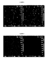
- FIG. 7 shows a WDX mapping image of the ceramic layer at the center of the laminate.
- FIG. 7 particularly shows the segregation state of different phases (Mg and Si). These heterophases are indicated by relatively bright spots in FIG.
- Additive elements (Mg, Si, etc.) added to the ceramic constituting the ceramic layer are easily segregated after heat treatment, and the segregated heterogeneous phase often adversely affects the reliability of the ceramic layer.
- the segregation of the additive element is very small as compared with the comparative example. Therefore, according to the example, it can be seen that the characteristics are stable.
- FIG. 8 shows the lead-out portion of the internal electrode.
- the internal electrode was made thinner, but the amount of retraction at the lead-out portion was very small, and sintering was completed in a short time. For this reason, the movement and precipitation of the glass phase to the surface due to the additive component hardly occur. Therefore, when forming the external electrode, it is possible to omit the process for exposing the lead end portion of the internal electrode.
- Experimental Example 2 (Relationship between heating rate and electrode thickness) As shown in Table 2 below, the temperature increase rate was variously changed, and the minimum electrode thickness at which coverage of 80% or more was obtained in the internal electrode was determined.
- two types of samples were prepared, one using an Ni foil (Ni foil electrode) and one using a conductive paste containing Ni spherical powder (Ni spherical electrode) as an internal electrode. did.
- the conductive paste containing Ni spherical powder a paste having a relatively low filling rate of about 40 to 50% was used.
- Ni electrode A is a Ni foil electrode
- Ni electrode B is a Ni spherical electrode
- the thinning of the internal electrode is affected by the gap at the interface between the ceramic layer and the internal electrode. As shown in Table 2 and FIG. 9, at a heating rate of 15 ° C./second or less, the restraining force for the internal electrode having an electrode thickness of 0.3 ⁇ m or less cannot be maintained, and it is difficult to ensure coverage of 80% or more. On the other hand, since the ceramic is sintered and contracted in a short time by setting the temperature raising rate to 40 ° C./second or more, it is possible to ensure a coverage of 80% or more even at an electrode thickness of 0.3 ⁇ m or less. . Furthermore, by setting the rate of temperature rise to 100 ° C./second or more, 80% or more coverage can be secured even with an electrode thickness of 0.1 ⁇ m or less.
- the level of electrode thickness as described above varies depending on the filling rate of the conductive paste used.
- the electrode thickness must be relatively thick in order to ensure a predetermined coverage.
- Ni was used as the conductive component of the internal electrode, but the same applies to Cu, Ag, Pt, Pd, Al, Ti, Cr or alloys thereof other than Ni. There is a trend.
- the residual rate variation due to the size of the laminate can be reduced by increasing the rate of temperature rise, and in particular by setting the rate of temperature rise to 40 ° C./second or more, the residual rate variation is 1% or less. It can be seen that it can be suppressed.
- Experimental Example 4 (Relationship between maximum temperature holding time and electrode coverage) As described above, according to the present invention, it is possible to reduce the thickness of the internal electrode and increase the coverage, but these are also affected by the maximum temperature holding time in addition to the rate of temperature increase.
- FIG. 10 in order to obtain a multilayer body for a multilayer ceramic capacitor having an Ni internal electrode corresponding to an electrode thickness of 0.3 ⁇ m, after reaching 1380 ° C. at a temperature rising rate of 40 ° C./second, The relationship between retention time and electrode coverage is shown.
- Experimental Example 5 (Relationship between heating rate and Ni electrode oxidation degree)
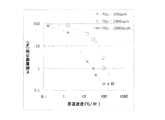
- oxygen partial pressure (PO 2 ) in the heat treatment step three atmospheres of 100 ppm, 1000 ppm and 10000 ppm were adopted as shown in Table 4 and FIG. Table 4 and FIG. 11 show the relationship between the average temperature increase rate from room temperature to the maximum temperature under three oxygen partial pressures of 100 ppm, 1000 ppm, and 10000 ppm and the Ni electrode oxidation degree. These oxygen partial pressures were adjusted by introducing a predetermined amount of oxygen into the nitrogen atmosphere.
- Experimental Example 6 Influence of boundary surface between large grain region and small grain region
- samples 1 to 4 were prepared and evaluated for multilayer ceramic capacitors having a normal rectangular parallelepiped shape.
- the outline of Samples 1 to 4 is as follows.
- Sample 1 is an example within the scope of the present invention, and a boundary surface exists inside each of the LW surface and the LT surface.
- Samples 2 to 4 are comparative examples outside the scope of the present invention. In particular, sample 2 has a boundary surface only inside the LW surface, sample 3 has a boundary surface only inside the LT surface, and sample 4 has no boundary surface. is there.
- a ceramic green sheet B having a thickness of 5 ⁇ m was formed by the same method.
- a portion of the slurry prepared for forming the ceramic green sheet B was taken, and the solvent was partially removed to prepare a thickened ceramic slurry C.
- the ceramic slurry C was applied by a predetermined thickness on the surface to be the LT surface of the individual piece thus cut, and dried to set the side gap thickness to 145 ⁇ m on one side. Further cutting was performed to obtain a green laminated chip C.
- the green laminated chip A according to Sample 1 was fired under heating conditions of an average temperature rising rate of 40 ° C./second, a maximum temperature of 1300 ° C., and a maximum temperature holding time of 1 second.
- green laminated chips B, C, and D relating to each of Samples 2, 3, and 4 were fired under heating conditions of an average temperature rising rate of 0.17 ° C./second, a maximum temperature of 1220 ° C., and a maximum temperature holding time of 1 hour. did.
- the dimensions of the multilayer ceramic capacitor thus obtained were length L: 2.0 mm, width W: 1.2 mm, and thickness T: 1.2 mm.
- the thickness of the dielectric ceramic layer per layer was 2.0 ⁇ m.
- the area of the overlapping part of the internal electrodes was 2.0 mm 2 .
- the thickness of the outer layer portion was 120 ⁇ m, and the thickness of the side gap portion was 120 ⁇ m.
- FIG. 12 shows an SEM image obtained by imaging a cross section parallel to the LT surface of the multilayer ceramic capacitor multilayer body according to Sample 1.
- the upper end of FIG. 12 is at a distance of 60 ⁇ m from the outermost internal electrode, and the lower end of FIG. 12 is at a distance of 25 ⁇ m from the outermost internal electrode.
- FIG. 12 it is observed that the grain diameter distributions are different from each other inside and outside the boundary surface.
- the image analysis was performed on SEM photographs having an area per visual field of 12.5 ⁇ m 2 and 50 visual fields, and the grain diameter was determined. In each field of view, are arranged in ascending order of the grain diameter, total area of each grain, the grain diameter of the order reaching 80% of the entire field of view was defined as the 80 value D of the grain size distribution in its field of view.
- a region having a distance of 20 to 40 ⁇ m from the internal electrode corresponds to a region on the inner side of the boundary surface in the sample 1, for example.
- the maximum The values are shown in Table 6 as “maximum D 80 values in the 20-40 ⁇ m region”.
- the distance from the internal electrode is equivalent to 50 to 70 [mu] m in the region of the sample 1 at the boundary surface outer e.g. region of the D 80 value in this region, a minimum value, in Table 6, "50 ⁇ The value is shown as “Minimum D 80 value in 70 ⁇ m region”.
- Table 6 also shows the presence or absence of the boundary surface described above.
- the “maximum D 80 value in the 20 to 40 ⁇ m region” and the “minimum D 80 value in the 50 to 70 ⁇ m region” are naturally It shows the same value.
- the “minimum D 80 value in the 50 to 70 ⁇ m region” is larger than the “maximum D 80 value in the 20 to 40 ⁇ m region”.
- the latter “minimum D 80 value in the 50 to 70 ⁇ m region” was 5 times or more than the former “maximum D 80 value in the 20 to 40 ⁇ m region”.
- the capacitance (C DC0V ) of the multilayer ceramic capacitor according to each sample when no DC voltage is applied is measured at a temperature of 25 ° C. under the conditions of 120 Hz and 1.0 V using an automatic bridge type measuring instrument. did.
- the capacitance under application of a DC voltage was determined as the capacitance (C DC4V ) when a DC voltage of 4 V was applied for 1 second.
- the sample of the multilayer ceramic capacitor to be measured was heated at a temperature of 150 ° C. for 1 hour, and the voltage was applied at a temperature of 25 ° C. until the measurement was performed after the heating. The process which stored without applying is performed.
- the dielectric constant change rate ( ⁇ ) is small.
- the minimum "50 ⁇ 70 [mu] m region as compared with Sample 1 the boundary surface is present in both the outer portion and the side gap portion, and" maximum D 80 value of 20 ⁇ 40 [mu] m region " “D 80 value” indicates a large value. Therefore, as in Sample 1, the large grain region is located outside the small grain region, and the boundary surface between the large grain region and the grain region is outside the portion where the internal electrode exists, and the outer layer portion.
- the ceramic layer is located inside the outer surface of the laminate so as to extend along the side gap portion, it can be seen that the DC bias characteristics can be maintained well even when the ceramic layer is thinned.
- a temperature profile in which the average rate of temperature increase from room temperature to the maximum temperature is 40 ° C./second or more is used. It can be seen that it is effective to employ a heat treatment step.
Landscapes
- Engineering & Computer Science (AREA)
- Chemical & Material Sciences (AREA)
- Power Engineering (AREA)
- Manufacturing & Machinery (AREA)
- Ceramic Engineering (AREA)
- Microelectronics & Electronic Packaging (AREA)
- Inorganic Chemistry (AREA)
- Materials Engineering (AREA)
- Structural Engineering (AREA)
- Organic Chemistry (AREA)
- Ceramic Capacitors (AREA)
- Fixed Capacitors And Capacitor Manufacturing Machines (AREA)
Abstract
Description
この発明は、積層セラミック電子部品およびその製造方法に関するもので、特に、積層セラミック電子部品の小型化のために有利に採用され得る技術に関するものである。 The present invention relates to a multilayer ceramic electronic component and a method for manufacturing the same, and particularly to a technique that can be advantageously employed for miniaturization of the multilayer ceramic electronic component.
たとえば積層セラミックコンデンサにおいて、その小型化(薄型化)を図るにあたっては、セラミック層だけでなく、内部電極についても薄層化を図ることが有効である。しかしながら、内部電極の薄層化が進むと、生の積層体を焼結させるための焼成工程の結果、電極切れが生じやすくなる。この電極切れを抑制し得る技術として、たとえば以下のものが提案されている。 For example, in reducing the thickness (thinning) of a multilayer ceramic capacitor, it is effective to reduce not only the ceramic layer but also the internal electrode. However, when the internal electrode is made thinner, the electrode is likely to be cut off as a result of the firing step for sintering the green laminate. For example, the following techniques have been proposed as techniques that can suppress this electrode breakage.
特開2008‐226941号公報(特許文献1)では、焼成工程での昇温速度を500℃/時~5000℃/時とすることにより、電極切れを抑制し、電極厚0.8~1μmを実現している。 In Japanese Patent Application Laid-Open No. 2008-226941 (Patent Document 1), the rate of temperature increase in the firing step is set to 500 ° C./hour to 5000 ° C./hour, so that electrode breakage is suppressed, and the electrode thickness is 0.8 to 1 μm. Realized.
特開2000‐216042号公報(特許文献2)では、焼成時の昇温過程における700℃~1100℃で、昇温速度を500℃/時以上とし、1100℃以上において、雰囲気の酸素分圧を10-8atm以下とし、降温過程における1100℃以下の一部において酸素分圧を10-8atm以上とすることにより、クラック等の構造欠陥を抑制し、得られた積層セラミックコンデンサの信頼性を高めるようにしている。 In Japanese Patent Laid-Open No. 2000-216042 (Patent Document 2), the temperature rise rate is 700 ° C. to 1100 ° C. in the temperature raising process during firing, the temperature rising rate is 500 ° C./hour or higher, and the oxygen partial pressure in the atmosphere is 1100 ° C. or higher. and 10 -8 atm or less, by the oxygen partial pressure and 10 -8 atm or more at 1100 ° C. the following part of the cooling process, to suppress structural defects such as cracks, the reliability of the obtained multilayer ceramic capacitor I try to increase it.
大韓民国公開特許公報10‐2006‐0135249(特許文献3)では、最高温度より20℃低い温度まで10℃/秒の昇温速度で昇温することにより、電極切れ抑制と昇温時のオーバシュート(昇温時に所望の焼成温度よりさらに高い温度となること)抑制とを両立させている。
According to Korean Patent Laid-Open No. 10-2006-0135249 (Patent Document 3), by raising the temperature at a rate of temperature increase of 10 ° C./second to a
以上、特許文献1~3のいずれに記載の先行技術においても、昇温速度を高くするといった手段によって、内部電極の薄層化が可能となる効果が得られるが、その効果には限界があり、たとえばNiを導電成分として含む内部電極を備える積層セラミックコンデンサにおいて、焼成後の電極厚として0.3μm以下の実現は非常に困難である。
As described above, in any of the prior arts described in
また、卑金属を導電成分として用いた内部電極を備える生の積層体を焼成するための雰囲気は、たとえばN2/H2/H2O系であり、Ni/NiO平衡酸素分圧より還元側で制御する必要があり、このことは、設備や材料設計に対する制約となる。 An atmosphere for firing a raw laminate including an internal electrode using a base metal as a conductive component is, for example, an N 2 / H 2 / H 2 O system, which is closer to the reduction side than Ni / NiO equilibrium oxygen partial pressure. This needs to be controlled, which is a constraint on equipment and material design.
また、内部電極を薄層化するには、低温焼結するセラミック材料を使用することも有効である。低温焼結セラミック材料には、Li等の揮発成分を含ませることがあるが、焼成時において、この揮発成分は飛散しやすい傾向がある。そして、焼成されるべき生の積層体のサイズ、すなわちチップサイズや焼成炉へのチャージ量により、揮発成分の残留量がばらつきやすいが、この残留量ばらつきを抑制することは困難である。 It is also effective to use a ceramic material that is sintered at a low temperature in order to make the internal electrode thin. The low-temperature sintered ceramic material may contain a volatile component such as Li, but this volatile component tends to be scattered during firing. The residual amount of the volatile component tends to vary depending on the size of the raw laminate to be fired, that is, the chip size and the amount of charge to the firing furnace, but it is difficult to suppress this variation in the residual amount.
他方、前述したように、セラミック層の薄層化も、積層セラミックコンデンサの小型化のために有効である。しかし、セラミック層の薄層化は、次のような問題を招くことがある。 On the other hand, as described above, thinning the ceramic layer is also effective for reducing the size of the multilayer ceramic capacitor. However, the thinning of the ceramic layer may cause the following problems.
セラミック層の薄層化が進めば進むほど、セラミック層に印加される直流電界強度がより高くなる。一般に、単位体積あたりの静電容量が比較的高い積層セラミックコンデンサのセラミック層には、強誘電体セラミックが用いられている。しかし、強誘電体セラミックは、そこに大きな直流電圧が印加されると、その誘電率が低下するという性質を有している。さらに、強誘電体セラミックには、その誘電率が高い方が、また、印加される直流電界強度が高い方が、直流電圧印加による誘電率の低下率が高くなる傾向がある。 The thinner the ceramic layer is, the higher the DC electric field strength applied to the ceramic layer. In general, a ferroelectric ceramic is used for a ceramic layer of a multilayer ceramic capacitor having a relatively high capacitance per unit volume. However, the ferroelectric ceramic has a property that its dielectric constant decreases when a large DC voltage is applied thereto. Further, the ferroelectric ceramic tends to have a higher rate of decrease in dielectric constant due to application of a DC voltage when the dielectric constant is higher and when the applied DC electric field strength is higher.
現状において要求されるセラミック層の薄層化は、それを進めた結果、セラミック層の厚さあたりの直流電圧が高くなり、それにより、誘電体セラミックの直流電圧下での誘電率が低下してしまい、積層セラミックコンデンサの直流電圧下での静電容量がかえって低下するほどのものとなってきている。すなわち、セラミック層の薄層化を進めても、積層セラミックコンデンサの大容量化を図ることが困難な状況にまで、セラミック層の薄層化が既に進んでいる。 As a result of the progress of thinning of the ceramic layer that is currently required, the direct current voltage per thickness of the ceramic layer becomes higher, which decreases the dielectric constant of the dielectric ceramic under the direct current voltage. As a result, the capacitance of the multilayer ceramic capacitor under a direct current voltage is reduced. That is, even if the ceramic layer is made thinner, the ceramic layer has already been made thinner to the point where it is difficult to increase the capacity of the multilayer ceramic capacitor.
そこで、印加される直流電界強度が高くなっても、誘電体セラミックの誘電率が低下しにくい、すなわち、DCバイアス特性の優れた、積層セラミックコンデンサが求められる。たとえば、特開2006-165259号公報(特許文献4)に記載の技術では、DCバイアス特性を改善するために、材料組成を検討している。しかし、材料組成を変更する場合は、他の諸特性(誘電率、温度特性、信頼性など)とのバランスをとるのが難しく、設計の幅を狭めてしまうという問題を招く。 Therefore, there is a demand for a multilayer ceramic capacitor in which the dielectric constant of the dielectric ceramic is unlikely to decrease even when the applied DC electric field strength is high, that is, excellent in DC bias characteristics. For example, in the technique described in Japanese Patent Application Laid-Open No. 2006-165259 (Patent Document 4), the material composition is examined in order to improve the DC bias characteristics. However, when changing the material composition, it is difficult to balance with other characteristics (dielectric constant, temperature characteristics, reliability, etc.), which causes a problem of narrowing the design range.
なお、上述した課題は、積層セラミックコンデンサについてのものであったが、同様の課題は、積層セラミックコンデンサ以外の積層セラミック電子部品についても遭遇し得る。 In addition, although the subject mentioned above was a thing about a multilayer ceramic capacitor, the same subject can be encountered also about multilayer ceramic electronic components other than a multilayer ceramic capacitor.
そこで、この発明の目的は、上述したような問題を解決し得る積層セラミック電子部品およびその製造方法を提供しようとすることである。 Therefore, an object of the present invention is to provide a multilayer ceramic electronic component that can solve the above-described problems and a method for manufacturing the same.
この発明は、積層された複数のセラミック層とセラミック層間の特定の界面に沿って形成される内部電極とを備える、積層体と、特定の内部電極と電気的に接続されるように積層体の外表面上に形成される外部電極とを備える、積層セラミック電子部品にまず向けられるものであって、上述した技術的課題を解決するため、次のような構成を備えることを特徴としている。 The present invention includes a laminated body including a plurality of laminated ceramic layers and internal electrodes formed along a specific interface between the ceramic layers, and the laminated body so as to be electrically connected to the specific internal electrodes. The multilayer electrode is first directed to a multilayer ceramic electronic component including an external electrode formed on an outer surface, and is characterized by having the following configuration in order to solve the technical problem described above.
すなわち、上記積層体は、セラミック層を構成するセラミックのグレイン径に関して、これが比較的大きい大グレイン領域と比較的小さい小グレイン領域とに分類され、大グレイン領域は小グレイン領域の外側に位置し、大グレイン領域と小グレイン領域との境界面は、積層体における内部電極の存在する部分を囲みながら積層体の外表面の内側に位置していることを特徴としている。なお、上記境界面が、積層体における、外部電極と内部電極との接続部分に存在するか否かは問わない。 That is, the laminated body is classified into a relatively large large grain region and a relatively small small grain region with respect to the grain diameter of the ceramic constituting the ceramic layer, and the large grain region is located outside the small grain region, The boundary surface between the large grain region and the small grain region is characterized in that it is located inside the outer surface of the multilayer body while surrounding the portion where the internal electrode is present in the multilayer body. In addition, it does not ask | require whether the said interface exists in the connection part of an external electrode and an internal electrode in a laminated body.
この発明に係る積層セラミック電子部品のより特定的な実施態様では、上記積層体は、その長さ方向寸法Lおよびその幅方向寸法Wによって規定されるLW面と、その長さ方向寸法Lおよびその厚み方向寸法Tによって規定されるLT面と、その幅方向寸法Wおよびその厚み方向寸法Tによって規定されるWT面とを有する直方体形状であり、上記外部電極はWT面上に形成される。この場合、大グレイン領域と小グレイン領域との境界面は、積層体における内部電極の存在する部分の外側であって、少なくともLW面およびLT面に沿って連続的に延びるように積層体の外表面の内側に位置する。ここで、境界面が、WT面に沿うように延びるか否かは問わない。 In a more specific embodiment of the multilayer ceramic electronic component according to the present invention, the multilayer body has an LW surface defined by its lengthwise dimension L and its widthwise dimension W, its lengthwise dimension L and its It has a rectangular parallelepiped shape having an LT surface defined by a thickness direction dimension T, a width direction dimension W and a WT surface defined by the thickness direction dimension T, and the external electrode is formed on the WT surface. In this case, the boundary surface between the large grain region and the small grain region is outside the portion where the internal electrode exists in the multilayer body, and extends outside the multilayer body so as to continuously extend along at least the LW plane and the LT plane. Located inside the surface. Here, it does not matter whether the boundary surface extends along the WT surface.
この発明に係る積層セラミック電子部品において、より好ましくは、大グレイン領域でのセラミックのグレイン径分布におけるD80値は、小グレイン領域でのセラミックのグレイン径分布におけるD80値の5倍以上である。 In the multilayer ceramic electronic component according to the present invention, more preferably, the D 80 value in the grain diameter distribution of the ceramic in the large grain region is 5 times or more than the D 80 value in the grain diameter distribution of the ceramic in the small grain region. .
この発明は、また、積層された複数のセラミック層とセラミック層間の特定の界面に沿って形成される内部電極とを備える、生の積層体を用意する工程と、生の積層体を焼結させるため、焼成する工程とを備える、積層セラミック電子部品の製造方法にも向けられる。この発明に係る積層セラミック電子部品の製造方法は、前述した技術的課題を解決するため、焼成する工程において、室温から最高温度までの平均昇温速度を40℃/秒以上とする温度プロファイルにて熱処理する工程を実施することを特徴としている。 The present invention also includes a step of preparing a raw laminate including a plurality of laminated ceramic layers and internal electrodes formed along a specific interface between the ceramic layers, and sintering the raw laminate. Therefore, the present invention is also directed to a method for manufacturing a multilayer ceramic electronic component including a firing step. In order to solve the above-described technical problem, the method for manufacturing a multilayer ceramic electronic component according to the present invention has a temperature profile in which an average temperature increase rate from room temperature to the maximum temperature is 40 ° C./second or more in the firing step. It is characterized by performing a heat treatment step.
上記熱処理する工程は、好ましくは、室温から最高温度までの平均昇温速度を100℃/秒以上とする温度プロファイルにて実施される。 The above heat treatment step is preferably performed with a temperature profile in which the average rate of temperature rise from room temperature to the maximum temperature is 100 ° C./second or more.
熱処理する工程の前に、生の積層体を脱脂する工程をさらに備えることが好ましい。 It is preferable to further include a step of degreasing the raw laminate before the heat treatment step.
内部電極が導電成分として卑金属を含む場合であっても、熱処理する工程は、卑金属の平衡酸素分圧に対して酸化側の雰囲気ガスを供給した雰囲気中で実施されることが好ましい。 Even if the internal electrode contains a base metal as a conductive component, the heat treatment step is preferably performed in an atmosphere in which an atmospheric gas on the oxidation side is supplied with respect to the equilibrium oxygen partial pressure of the base metal.
熱処理する工程において、最高温度到達後、温度保持することなく、冷却されることが好ましい。 In the heat treatment step, after reaching the maximum temperature, it is preferable to cool without holding the temperature.
この発明に係る積層セラミック電子部品によれば、セラミック層が薄層化されても、DCバイアス特性を良好に維持することができる。特に、この発明が積層セラミックコンデンサに適用される場合には、直流電圧印加による静電容量の低下率を低く抑えることができるとともに、セラミック層において、比較的高い誘電率を得ることができる。このような効果は、次のようなメカニズムによってもたらされるものと推測される。 According to the multilayer ceramic electronic component according to the present invention, the DC bias characteristics can be maintained well even when the ceramic layer is thinned. In particular, when the present invention is applied to a multilayer ceramic capacitor, the rate of decrease in capacitance due to application of a DC voltage can be kept low, and a relatively high dielectric constant can be obtained in the ceramic layer. Such an effect is presumed to be brought about by the following mechanism.
境界面の外側にある大グレイン領域は、境界面の内側にある小グレイン領域と比較して、BaTiO3系強誘電体に見られる強誘電性が大きいと考えられる。このため、焼成後の冷却時において高温相(常誘電相)から常温相(強誘電相)に相転移が生じる際に、境界面の外側の領域における結晶のc軸方向が積層体の表面に対し垂直方向に配向しやすくなり、表面に垂直な応力が積層体内部に向かって発生すると推測される。 The large grain region outside the boundary surface is considered to have a larger ferroelectricity as seen in the BaTiO 3 ferroelectrics than the small grain region inside the boundary surface. For this reason, when the phase transition occurs from the high-temperature phase (paraelectric phase) to the normal temperature phase (ferroelectric phase) during cooling after firing, the c-axis direction of the crystal in the region outside the boundary surface is on the surface of the laminate. On the other hand, it becomes easy to orient in the vertical direction, and it is assumed that stress perpendicular to the surface is generated toward the inside of the laminate.
このとき、境界面の内側のセラミック層において面内方向収縮を喚起する応力がかかると推測され、結晶のc軸方向が積層方向と平行な方向へ配向する応力が喚起されると推測される。 At this time, it is presumed that a stress that induces in-plane direction shrinkage is applied to the ceramic layer inside the boundary surface, and it is presumed that a stress in which the c-axis direction of the crystal is oriented in a direction parallel to the stacking direction is induced.
このような状態において、積層セラミック電子部品に直流電圧が印加された場合、直流電圧により電界強度の方向と結晶のc軸方向が平行になる場合が多いため、電界がセラミック層に印加されても、誘電率はさほど低下しないものと推測される。 In such a state, when a DC voltage is applied to the multilayer ceramic electronic component, the direction of the electric field strength and the c-axis direction of the crystal are often parallel due to the DC voltage, so even if an electric field is applied to the ceramic layer. It is estimated that the dielectric constant does not decrease so much.
なお、内部電極の存在する部分が境界面によって部分的にしか覆われていない場合(たとえば、境界面がLT面の内側のみ、またはLW面の内側のみに形成されている場合)、上記現象により生じると推測される応力が分散してしまうと推測される。よって、この場合には、この発明の目的は十分には達成されない。 When the portion where the internal electrode exists is only partially covered by the boundary surface (for example, when the boundary surface is formed only inside the LT surface or only inside the LW surface), the above phenomenon occurs. It is presumed that the stress estimated to occur is dispersed. Therefore, in this case, the object of the present invention is not sufficiently achieved.
また、外部電極が形成されている付近(たとえば、WT面の内側など)は、境界面の形成が不十分でも問題はない。外部電極により応力分散が防がれるためであると推測される。 Also, in the vicinity where the external electrode is formed (for example, inside the WT surface), there is no problem even if the boundary surface is insufficiently formed. This is presumed to be because stress dispersion is prevented by the external electrode.
この発明に係る積層セラミック電子部品の製造方法によれば、積層体において、上述したような特徴あるグレイン径分布を有利に実現することができる。 According to the method for manufacturing a multilayer ceramic electronic component according to the present invention, the characteristic grain diameter distribution as described above can be advantageously realized in the multilayer body.
また、この発明に係る積層セラミック電子部品の製造方法によれば、内部電極において、熱処理中の電極切れや玉化等の状態変化が抑制され、内部電極の薄層化および高カバレッジ化を進めることができる。従来の熱処理方法では、たとえば、Niを導電成分として含む内部電極を備える積層セラミックコンデンサの場合、内部電極について、0.3μm以下の電極厚および80%以上のカバレッジの実現は非常に困難であったが、この発明に係る製造方法によれば、40℃/秒以上の昇温速度を採用することにより、0.2μm以下の電極厚および80%以上のカバレッジを達成することができる。さらに、昇温速度を100℃/秒以上と高めると、0.1μm以下の電極厚において80%以上のカバレッジを達成することができる。 In addition, according to the method for manufacturing a multilayer ceramic electronic component according to the present invention, in the internal electrode, state changes such as electrode breakage and dizziness during heat treatment are suppressed, and the internal electrode is made thinner and has higher coverage. Can do. In the conventional heat treatment method, for example, in the case of a multilayer ceramic capacitor including an internal electrode containing Ni as a conductive component, it is very difficult to realize an electrode thickness of 0.3 μm or less and a coverage of 80% or more for the internal electrode. However, according to the manufacturing method according to the present invention, an electrode thickness of 0.2 μm or less and a coverage of 80% or more can be achieved by employing a heating rate of 40 ° C./second or more. Furthermore, when the rate of temperature increase is increased to 100 ° C./second or more, a coverage of 80% or more can be achieved at an electrode thickness of 0.1 μm or less.
熱処理中の電極切れおよび玉化は、セラミック層と内部電極との収縮タイミングのミスマッチにより発生する界面隙間が大きい場合や、与える熱エネルギー総量が大きい場合に、より顕著に発生する。よって、熱処理時における収縮が生じる時間を、従来の40~10分間から、この発明に係る製造方法によれば、120~5秒間と大幅に短縮することができることから、セラミック層と内部電極との界面隙間の発生を抑制することができる。また、最高温度到達後、温度保持することなく、すぐに冷却するようにすれば、熱エネルギー総量を削減することができ、電極切れおよび玉化の抑制により効果的である。 During the heat treatment, electrode breakage and spheroidization occur more prominently when the interfacial gap generated due to the mismatch in shrinkage timing between the ceramic layer and the internal electrode is large or when the total amount of heat energy applied is large. Therefore, the time during which shrinkage occurs during the heat treatment can be greatly reduced from the conventional 40 to 10 minutes to 120 to 5 seconds according to the manufacturing method according to the present invention. Generation of an interfacial gap can be suppressed. Further, if the cooling is performed immediately after the maximum temperature is reached without maintaining the temperature, the total amount of heat energy can be reduced, which is more effective in suppressing electrode breakage and ball formation.
また、内部電極の薄層化および高カバレッジ化は、内部電極の収縮抑制の結果もたらされたものであるため、内部電極の端部におけるボイドや隙間等の発生も同時に抑制することができる。したがって、熱処理後の積層体のシール性が向上し、積層セラミック電子部品としての耐環境信頼性も向上させることができる。 Moreover, since the thinning and high coverage of the internal electrode are brought about as a result of suppressing the shrinkage of the internal electrode, it is possible to simultaneously suppress the generation of voids and gaps at the end of the internal electrode. Therefore, the sealing performance of the laminated body after the heat treatment is improved, and the environmental reliability as the multilayer ceramic electronic component can be improved.
また、上記のように内部電極の収縮が抑制されるため、内部電極が積層体の所定の面に引き出される場合、内部電極の引出し端部での引っ込み度合いが非常に小さくなる。また、前述したように、短時間で焼結が完了するため、セラミック層を構成するセラミックの添加成分によるガラス相の表面への移動および析出がほとんど発生しない。したがって、内部電極に電気的に接続される外部電極を形成するにあたって、内部電極の引出し端部を露出させるための工程を省略することができる。 In addition, since the contraction of the internal electrode is suppressed as described above, when the internal electrode is pulled out to a predetermined surface of the laminate, the degree of retraction at the leading end of the internal electrode becomes very small. Further, as described above, since the sintering is completed in a short time, the migration and precipitation to the surface of the glass phase due to the ceramic additive component constituting the ceramic layer hardly occur. Therefore, when forming the external electrode that is electrically connected to the internal electrode, the step for exposing the lead end of the internal electrode can be omitted.
また、短時間で焼結が完了するため、セラミック層を構成するセラミックにおける添加元素を偏析させることなく均一に存在させることができる。そのため、セラミック層が与える特性を安定させることができる。さらに、比較的少ない添加量であっても、添加元素による効果を十分に発揮させることができる。 Further, since the sintering is completed in a short time, the additive elements in the ceramic constituting the ceramic layer can be present uniformly without segregation. Therefore, the characteristics given by the ceramic layer can be stabilized. Furthermore, even with a relatively small addition amount, the effect of the additive element can be sufficiently exhibited.
また、セラミック層を構成するセラミックが、Li、B、Pb等の揮発成分(焼結助剤)を含有する場合、短時間で焼結が完了するため、熱処理時のそれら揮発成分の飛散が抑制される。その結果、これら揮発成分の残留量が、積層体のサイズや焼成炉へのチャージ量が変わることによって変動することを抑制することができる。 In addition, when the ceramic constituting the ceramic layer contains volatile components (sintering aids) such as Li, B, and Pb, since the sintering is completed in a short time, scattering of these volatile components during heat treatment is suppressed. Is done. As a result, it is possible to suppress the residual amount of these volatile components from fluctuating due to the change in the size of the laminate and the charge amount to the firing furnace.
また、Niなどの卑金属を導電成分として含む内部電極を備える積層セラミック電子部品にあっては、従来、熱処理工程において、内部電極酸化抑制とセラミック還元抑制とを両立させるため、雰囲気中の酸素分圧を卑金属の平衡酸素分圧近傍に精密に制御する必要があり、焼成炉の設計を煩雑なものとしていた。これに対し、この発明に係る製造方法によれば、熱処理工程において昇温速度が高く、熱処理(セラミック焼結収縮)時間が120~5秒間と短時間であるため、卑金属の平衡酸素分圧より酸化側の雰囲気でも、ほとんど酸化することなく、熱処理を行なうことができる。たとえば、昇温速度40℃/秒では、100ppm(平衡酸素分圧より約3.7桁酸化側/1300℃)、100℃/秒では1000ppm(平衡酸素分圧より約4.7桁酸化側/1300℃)というように、高い酸素分圧下で卑金属を含む内部電極をほとんど酸化させることなく、熱処理することができる。よって、セラミックが還元されにくく、また、再酸化処理する必要もなく、高い信頼性をもって積層セラミック電子部品を製造することができる。 In addition, in a multilayer ceramic electronic component having an internal electrode containing a base metal such as Ni as a conductive component, conventionally, in order to achieve both internal electrode oxidation suppression and ceramic reduction suppression in the heat treatment step, the oxygen partial pressure in the atmosphere Must be precisely controlled in the vicinity of the equilibrium oxygen partial pressure of the base metal, which makes the design of the firing furnace complicated. In contrast, according to the manufacturing method of the present invention, the rate of temperature rise is high in the heat treatment step, and the heat treatment (ceramic sintering shrinkage) time is as short as 120 to 5 seconds. Even in the atmosphere on the oxidation side, heat treatment can be performed with little oxidation. For example, at a rate of temperature increase of 40 ° C./second, 100 ppm (approximately 3.7 digits oxidation side from equilibrium oxygen partial pressure / 1300 ° C.), and at 100 ° C./second, 1000 ppm (approximately 4.7 digits oxidation side / from equilibrium oxygen partial pressure / (1300 ° C.), the internal electrode containing the base metal can be heat-treated under a high oxygen partial pressure with almost no oxidation. Therefore, it is difficult to reduce the ceramic, and it is not necessary to re-oxidize the multilayer ceramic electronic component with high reliability.
図1を参照して、この発明が適用される積層セラミック電子部品の一例としての積層セラミックコンデンサ1の構造について説明する。
Referring to FIG. 1, the structure of a multilayer
積層セラミックコンデンサ1は、部品本体としての積層体2を備えている。積層体2は、積層された複数のセラミック層3とセラミック層3間の特定の界面に沿って形成される複数の内部電極4および5とを備えている。積層体2の一方および他方端面6および7には、それぞれ、複数の内部電極4および5の各端部が露出していて、これら内部電極4の各端部および内部電極5の各端部を、それぞれ、互いに電気的に接続するように、外部電極8および9が形成されている。
The multilayer
このような積層セラミックコンデンサ1を製造するにあたっては、まず、内部電極4および5が印刷されたセラミックグリーンシートを積層するといった周知の方法により、積層体2の生の状態のものが作製される。次いで、生の積層体を焼結させるため、焼成工程が実施される。次いで、焼結した積層体2の端面6および7上に、それぞれ、外部電極8および9が形成され、積層セラミックコンデンサ1が完成される。
In manufacturing such a multilayer
上述した焼成工程において、この発明では、室温から最高温度までの平均昇温速度を40℃/秒以上とする温度プロファイルが適用された熱処理工程が実施される。好ましくは、上記温度プロファイルは100℃/秒以上とされる。 In the above-described firing step, in the present invention, a heat treatment step is applied in which a temperature profile is applied in which the average rate of temperature increase from room temperature to the maximum temperature is 40 ° C./second or more. Preferably, the temperature profile is 100 ° C./second or more.
また、上述の熱処理工程の前に、生の積層体は脱脂処理されることが好ましい。 Moreover, it is preferable that the raw laminate is degreased before the above heat treatment step.
内部電極4および5が導電成分としてNiのような卑金属を含むとき、熱処理工程は、卑金属の平衡酸素分圧に対して酸化側の雰囲気ガスを供給した雰囲気中で実施されてもよい。
When the
また、熱処理工程において、前述した最高温度到達後、この温度を保持することなく、直ちに冷却されることが好ましい。 In the heat treatment step, it is preferable that the temperature is immediately cooled without maintaining this temperature after reaching the above-mentioned maximum temperature.
これらの好ましい条件が採用される理由については、後述する実験例において明らかにする。 The reason why these preferable conditions are adopted will be clarified in an experimental example described later.
上述した製造方法、特に上述した焼成工程を採用したとき、得られた積層セラミック電子部品の積層体において、図2を参照して以下に説明するようなセラミックのグレイン径分布が実現される。 When the above-described manufacturing method, particularly the firing step described above, is adopted, the ceramic grain diameter distribution as described below with reference to FIG. 2 is realized in the obtained multilayer ceramic electronic component laminate.
図2において、(A)は積層体12の長さ方向寸法Lおよび幅方向寸法Wによって規定されるLW面に平行な面に沿う断面図を示し、(B)は積層体12の長さ方向寸法Lおよび厚み方向寸法Tによって規定されるLT面に平行な面に沿う断面図を示し、(C)は積層体12の幅方向寸法Wおよび厚み方向寸法Tによって規定されるWT面に平行な面に沿う断面図を示している。積層体12は、上記LW面と上記LT面と上記WT面とを有する直方体形状である。
2A shows a cross-sectional view along a plane parallel to the LW plane defined by the lengthwise dimension L and the widthwise dimension W of the laminate 12, and FIG. 2B shows the longitudinal direction of the laminate 12. A sectional view along a plane parallel to the LT plane defined by the dimension L and the thickness direction dimension T is shown, and (C) is parallel to the WT plane defined by the width direction dimension W and the thickness direction dimension T of the laminate 12. A cross-sectional view along the plane is shown. The
積層体12は、図2では図示されないが、積層された複数のセラミック層とセラミック層間の特定の界面に沿って形成される内部電極とを備えている。また、図2では図示されないが、特定の内部電極と電気的に接続されるように、外部電極が積層体12の外表面上に形成されている。
Although not shown in FIG. 2, the laminate 12 includes a plurality of laminated ceramic layers and internal electrodes formed along a specific interface between the ceramic layers. Although not shown in FIG. 2, external electrodes are formed on the outer surface of the
図2では図示されない上記セラミック層、内部電極ならびに外部電極は、図1に示したセラミック層3、内部電極4および5ならびに外部電極8および9に相当する。セラミック層および内部電極の各々の面方向は、たとえば上記LW面と平行であり、外部電極は上記WT面上に形成される。
The ceramic layer, internal electrodes and external electrodes not shown in FIG. 2 correspond to the
図2に示すように、積層体12は、セラミック層を構成するセラミックのグレイン径に関して、これが比較的大きい大グレイン領域13と比較的小さい小グレイン領域14とに分類される。ここで、大グレイン領域13でのセラミックのグレイン径分布におけるD80値は、小グレイン領域14でのセラミックのグレイン径分布におけるD80値の5倍以上であることが好ましい。
As shown in FIG. 2, the
大グレイン領域13は小グレイン領域14の外側に位置している。大グレイン領域13と小グレイン領域14との境界面15は、積層体12における内部電極の存在する素子部分16の外側であって、積層体12の外表面の内側に位置している。前述したように、外部電極がWT面上に形成される場合、境界面15は、好ましくは、少なくともLW面およびLT面に沿って連続的に延びている。
The
言い換えると、積層体12の外表面におけるLW面およびLT面は大グレイン領域13内にあり、LW面およびLT面の各々の内側には境界面15が存在することになる。すなわち、積層体12における、積層方向での両端部に相当する外層部のどこかに境界面15が存在し、内部電極の両側に形成されるサイドギャップ部のどこかに境界面15が存在することになる。
In other words, the LW surface and the LT surface on the outer surface of the laminate 12 are in the
しかし、外部電極が形成されたWT面には内部電極が引き出されているため、WT面での境界面による作用は、LW面やLT面での境界面15による作用に比べて小さい。よって、WT面に沿って境界面15が形成されるかどうかは問わない。
However, since the internal electrode is drawn out to the WT surface on which the external electrode is formed, the action of the boundary surface on the WT surface is smaller than the action of the
この発明が、上述したように、図1に示した積層セラミックコンデンサ1の製造に向けられるとき、セラミック層3は、誘電体セラミックから構成される。しかしながら、この発明が適用されるのは、積層セラミックコンデンサに限らず、その他、インダクタ、サーミスタ、圧電部品などであってもよい。したがって、積層セラミック電子部品の機能に応じて、セラミック層は、誘電体セラミックのほか、磁性体セラミック、半導体セラミック、圧電体セラミックなどから構成されてもよい。
As described above, when the present invention is directed to the manufacture of the multilayer
また、図1に示した積層セラミックコンデンサ1は、2個の外部端子8および9を備える2端子型のものであったが、多端子型の積層セラミック電子部品にもこの発明を適用することができる。
The multilayer
また、この発明は、直方体形状の積層体を備える積層セラミック電子部品に限らず、直方体形状以外の形状の積層体を備える積層セラミック電子部品にも適用されることができる。 Further, the present invention is not limited to a multilayer ceramic electronic component having a rectangular parallelepiped laminate, but can be applied to a multilayer ceramic electronic component having a laminate having a shape other than a rectangular parallelepiped shape.
以下に、この発明の範囲内にある実施例および範囲外の比較例の各々に従って、試料となる積層セラミックコンデンサを作製し、その評価を行なった実験例について説明する。 Hereinafter, experimental examples in which a multilayer ceramic capacitor as a sample was manufactured and evaluated according to each of the examples within the scope of the present invention and comparative examples outside the scope will be described.
1.実験例1(典型的熱処理条件下での実施例および比較例の比較)
Niを導電成分として含む内部電極およびBaTiO3を主成分とするセラミック層を備える積層セラミックコンデンサのための生の積層体を、残留カーボン量が約1000重量ppmとなるまで脱脂処理した後、以下の表1に示すような熱処理条件にて熱処理し、実施例および比較例の各々に係る焼結後の積層体を得た。
1. Experimental Example 1 (Comparison of Examples and Comparative Examples under Typical Heat Treatment Conditions)
A raw laminate for a multilayer ceramic capacitor having an internal electrode containing Ni as a conductive component and a ceramic layer mainly composed of BaTiO 3 is degreased until the residual carbon content is about 1000 ppm by weight, and then the following It heat-processed on the heat processing conditions as shown in Table 1, and obtained the laminated body after the sintering which concerns on each of an Example and a comparative example.

表1において、「昇温速度」は、室温から最高温度までの平均昇温速度を示している。図3は、実施例と比較例との相対比較を容易にするため、各々の温度プロファイルを図示したものである。 In Table 1, “temperature increase rate” indicates an average temperature increase rate from room temperature to the maximum temperature. FIG. 3 shows each temperature profile in order to facilitate relative comparison between the example and the comparative example.
上記熱処理により焼結した実施例および比較例の各々に係る積層体試料を評価した結果が図4ないし図8に示されている。 Results of evaluating the laminate samples according to each of the examples and comparative examples sintered by the heat treatment are shown in FIGS.
図4には、積層体の中央部での内部電極の厚み方向断面が示されている。図4において、相対的に濃い色の領域が内部電極である。図4から、比較例に比べ、実施例によれば、内部電極の連続性を確保しながら、より薄層化が図られていることがわかる。 FIG. 4 shows a cross section in the thickness direction of the internal electrode at the center of the laminate. In FIG. 4, the relatively dark color area is the internal electrode. From FIG. 4, it can be seen that, compared to the comparative example, the embodiment achieves a thinner layer while ensuring the continuity of the internal electrodes.
図5には、積層体の中央部での内部電極の表面状態が示されている。図5において、相対的に濃い色のスポットが内部電極の欠乏部分である。図5から、比較例に比べて、実施例によれば、内部電極の高カバレッジ化が図られていることがわかる。 FIG. 5 shows the surface state of the internal electrode at the center of the laminate. In FIG. 5, a relatively dark spot is a deficient portion of the internal electrode. From FIG. 5, it can be seen that, according to the example, higher coverage of the internal electrode is achieved as compared with the comparative example.
図6には、内部電極の端部での厚み方向断面が示されている。図6において、相対的に薄い色の領域が内部電極である。図6から、比較例に比べて、実施例によれば、内部電極の端部でのボイドや隙間の発生が抑制されていることがわかる。 FIG. 6 shows a cross section in the thickness direction at the end of the internal electrode. In FIG. 6, the relatively light colored area is the internal electrode. From FIG. 6, it can be seen that, according to the example, generation of voids and gaps at the end of the internal electrode is suppressed as compared with the comparative example.
これら図4ないし図6に示した評価結果から、実施例によれば、積層体において高いシール性が得られ、そのため、積層セラミックコンデンサの耐環境信頼性を向上させ得ることがわかる。従来、外部電極に対して耐環境信頼性向上のためのシール機能が求められることがあったが、実施例によれば、積層体において高いシール性が得られるので、外部電極は内部電極との電気的接続を達成すれば足り、それゆえ、外部電極の形成にあたっての材料選択やプロセス設計が容易になるという利点も期待できる。 From these evaluation results shown in FIG. 4 to FIG. 6, it can be seen that according to the examples, high sealing performance can be obtained in the multilayer body, and therefore the environmental reliability of the multilayer ceramic capacitor can be improved. Conventionally, the external electrode has been required to have a sealing function for improving the environmental resistance reliability. However, according to the example, since a high sealing performance is obtained in the laminate, the external electrode is connected to the internal electrode. It is sufficient to achieve the electrical connection, and therefore, it is possible to expect the advantage that the material selection and the process design in forming the external electrode become easy.
図7には、積層体の中央部でのセラミック層のWDXマッピング像が示されている。図7では、特に異相(MgおよびSi)の偏析状態が示されている。これら異相は、図7において、相対的に明るいスポットによって示されている。セラミック層を構成するセラミックへの添加元素(Mg、Siなど)は、熱処理後に偏析しやすく、このように偏析した異相は、セラミック層の信頼性に悪影響を及ぼすことが多い。図7からわかるように、実施例によれば、比較例に比べて、添加元素の偏析が極めて少ない。よって、実施例によれば、特性が安定することがわかる。 FIG. 7 shows a WDX mapping image of the ceramic layer at the center of the laminate. FIG. 7 particularly shows the segregation state of different phases (Mg and Si). These heterophases are indicated by relatively bright spots in FIG. Additive elements (Mg, Si, etc.) added to the ceramic constituting the ceramic layer are easily segregated after heat treatment, and the segregated heterogeneous phase often adversely affects the reliability of the ceramic layer. As can be seen from FIG. 7, according to the example, the segregation of the additive element is very small as compared with the comparative example. Therefore, according to the example, it can be seen that the characteristics are stable.
図8には、内部電極の引出し部が示されている。図8からわかるように、比較例に比べて、実施例によれば、内部電極の薄層化ばかりでなく、引出し部での引っ込み量が非常に少なく、また、短時間で焼結が完了するため、添加成分によるガラス相の表面への移動および析出がほとんど発生していない。よって、外部電極形成時において、内部電極の引出し端部を露出させるための工程の省略も可能となる。 FIG. 8 shows the lead-out portion of the internal electrode. As can be seen from FIG. 8, compared to the comparative example, according to the example, not only the internal electrode was made thinner, but the amount of retraction at the lead-out portion was very small, and sintering was completed in a short time. For this reason, the movement and precipitation of the glass phase to the surface due to the additive component hardly occur. Therefore, when forming the external electrode, it is possible to omit the process for exposing the lead end portion of the internal electrode.
2.実験例2(昇温速度と電極厚との関係)
以下の表2に示すように、昇温速度を種々に変更し、内部電極においてカバレッジ80%以上が得られる最小電極厚を求めた。なお、この実験例2では、内部電極として、Ni箔を用いたもの(Ni箔電極)と、Ni球状粉末を含む導電性ペーストを用いたもの(Ni球状電極)との2種類の試料を作製した。なお、Ni球状粉末を含む導電性ペーストについては、充填率が40~50%程度の比較的低い充填率のものを用いた。
2. Experimental Example 2 (Relationship between heating rate and electrode thickness)
As shown in Table 2 below, the temperature increase rate was variously changed, and the minimum electrode thickness at which coverage of 80% or more was obtained in the internal electrode was determined. In Experimental Example 2, two types of samples were prepared, one using an Ni foil (Ni foil electrode) and one using a conductive paste containing Ni spherical powder (Ni spherical electrode) as an internal electrode. did. As the conductive paste containing Ni spherical powder, a paste having a relatively low filling rate of about 40 to 50% was used.

表2に示した昇温速度と電極厚との関係は図9にも示されている。図9において、「Ni電極A」はNi箔電極であり、「Ni電極B」はNi球状電極である。 The relationship between the heating rate and electrode thickness shown in Table 2 is also shown in FIG. In FIG. 9, “Ni electrode A” is a Ni foil electrode, and “Ni electrode B” is a Ni spherical electrode.
内部電極の薄層化は、セラミック層と内部電極との界面の隙間の影響を受ける。表2および図9に示すように、15℃/秒以下の昇温速度では、電極厚0.3μm以下の内部電極に対する拘束力を維持できず、カバレッジ80%以上の確保は困難である。これに対し、昇温速度を40℃/秒以上とすることにより、短時間でセラミックが焼結収縮するため、0.3μm以下の電極厚においても、80%以上のカバレッジを確保することができる。さらに、昇温速度を100℃/秒以上とすることにより、0.1μm以下の電極厚でも80%以上のカバレッジを確保することができる。 The thinning of the internal electrode is affected by the gap at the interface between the ceramic layer and the internal electrode. As shown in Table 2 and FIG. 9, at a heating rate of 15 ° C./second or less, the restraining force for the internal electrode having an electrode thickness of 0.3 μm or less cannot be maintained, and it is difficult to ensure coverage of 80% or more. On the other hand, since the ceramic is sintered and contracted in a short time by setting the temperature raising rate to 40 ° C./second or more, it is possible to ensure a coverage of 80% or more even at an electrode thickness of 0.3 μm or less. . Furthermore, by setting the rate of temperature rise to 100 ° C./second or more, 80% or more coverage can be secured even with an electrode thickness of 0.1 μm or less.
なお、導電性ペーストを用いたNi球状電極の場合には、上述したような電極厚の水準は、用いた導電性ペーストの充填率により変わる。この実験例で用いた比較的低い充填率の導電性ペーストの場合には、所定のカバレッジを確保し得るようにするためには、電極厚を比較的厚くしなければならない。 In the case of a Ni spherical electrode using a conductive paste, the level of electrode thickness as described above varies depending on the filling rate of the conductive paste used. In the case of the conductive paste having a relatively low filling rate used in this experimental example, the electrode thickness must be relatively thick in order to ensure a predetermined coverage.
この実験例では、内部電極の導電成分としてNiを用いた場合のものであったが、Ni以外のたとえばCu、Ag、Pt、Pd、Al、Ti、Crまたはそれらの合金であっても同様の傾向が見られる。 In this experimental example, Ni was used as the conductive component of the internal electrode, but the same applies to Cu, Ag, Pt, Pd, Al, Ti, Cr or alloys thereof other than Ni. There is a trend.
3.実験例3(昇温速度と揮発成分残留量との関係)
セラミック層を構成するセラミックが、Li、B、Pb等の揮発成分を含む場合、これら揮発成分の熱処理後における残留量は、積層体のサイズや熱処理時の焼成炉への積層体のチャージ量によって変動することが経験的に知られている。したがって、この変動が、実用化段階においては、特性の安定を阻害するといった問題を招く。しかしながら、この発明のように、昇温速度を高くすることにより、セラミックの焼結収縮時間を短時間化することができるため、揮発成分の残留量の変動を大幅に抑制することができる。
3. Experimental Example 3 (Relationship between heating rate and residual amount of volatile components)
When the ceramic constituting the ceramic layer contains volatile components such as Li, B, and Pb, the residual amount of these volatile components after heat treatment depends on the size of the laminate and the amount of charge of the laminate to the firing furnace during heat treatment. It is empirically known to fluctuate. Therefore, this variation causes a problem that the stability of characteristics is hindered in the practical application stage. However, since the sintering shrinkage time of the ceramic can be shortened by increasing the rate of temperature increase as in the present invention, fluctuations in the residual amount of volatile components can be significantly suppressed.
以下の表3には、揮発成分の残留率(=残留量/添加量)に対する昇温速度による影響が示されている。より具体的には、積層体の平面サイズが0.6mm×0.3mm(0603サイズ)の場合と3.2mm×2.5mm(3225サイズ)の場合とについて評価した揮発成分残留率と昇温速度との関係が示されるとともに、「0603サイズ」と「3225サイズ」との各々の揮発成分残留率の差が「残留率ばらつき」として示されている。 Table 3 below shows the influence of the rate of temperature rise on the residual rate of volatile components (= residual amount / added amount). More specifically, the volatile component residual ratio and the temperature rise evaluated when the planar size of the laminate is 0.6 mm × 0.3 mm (0603 size) and 3.2 mm × 2.5 mm (3225 size). The relationship with the speed is shown, and the difference in volatile component residual ratio between “0603 size” and “3225 size” is shown as “residual ratio variation”.

表3から、積層体のサイズによる残留率ばらつきは、昇温速度をより高くすることによって低減することができ、特に昇温速度40℃/秒以上とすることにより、残留率ばらつきを1%以下に抑制できることがわかる。 From Table 3, the residual rate variation due to the size of the laminate can be reduced by increasing the rate of temperature rise, and in particular by setting the rate of temperature rise to 40 ° C./second or more, the residual rate variation is 1% or less. It can be seen that it can be suppressed.
上述のような傾向は、熱処理時の積層体のチャージ量を変えた場合にも同様に見られる。 The same tendency as described above can be seen when the charge amount of the laminate during the heat treatment is changed.
4.実験例4(最高温度保持時間と電極カバレッジとの関係)
上述したように、この発明によれば、内部電極の薄層化および高カバレッジ化を実現できるが、これらは、昇温速度に加えて、最高温度保持時間によっても影響される。図10には、電極厚0.3μm相当のNi内部電極を有する積層セラミックコンデンサのための積層体を得るため、昇温速度40℃/秒で1380℃にまで到達した後、この1380℃での保持時間と電極カバレッジとの関係が示されている。
4). Experimental Example 4 (Relationship between maximum temperature holding time and electrode coverage)
As described above, according to the present invention, it is possible to reduce the thickness of the internal electrode and increase the coverage, but these are also affected by the maximum temperature holding time in addition to the rate of temperature increase. In FIG. 10, in order to obtain a multilayer body for a multilayer ceramic capacitor having an Ni internal electrode corresponding to an electrode thickness of 0.3 μm, after reaching 1380 ° C. at a temperature rising rate of 40 ° C./second, The relationship between retention time and electrode coverage is shown.
図10に示すように、昇温速度を高めることにより、1380℃到達直後では高いカバレッジが達成されている。しかし、この1380℃といった最高温度を保持することにより、急激にカバレッジが低下(玉化)することがわかる。これは、急激な昇温中においては、内部電極への拘束力を維持できるが、収縮を完了した最高温度付近では、セラミックに強度はなく、柔らかい状態であるため、温度保持により、内部電極の表面エネルギーを最小にしようとする駆動力が働き、この駆動力によってもたらされる玉化に対抗することができず、その結果、カバレッジが低下することになると考えられる。特に、上記駆動力は、電極厚が薄くなるほど、表面の割合が増加するため、より顕著になる。したがって、最高温度到達後は、その温度を保持することなく、直ちに冷却することが望ましい。 As shown in FIG. 10, high coverage is achieved immediately after reaching 1380 ° C. by increasing the heating rate. However, it can be seen that by maintaining the maximum temperature such as 1380 ° C., the coverage is drastically lowered (balling). This is because the restraining force on the internal electrode can be maintained during the rapid temperature rise, but the ceramic is not strong and soft near the maximum temperature at which the shrinkage is completed. It is thought that the driving force that tries to minimize the surface energy works and cannot counter the spheroidization caused by this driving force, resulting in a decrease in coverage. In particular, the driving force becomes more prominent because the proportion of the surface increases as the electrode thickness decreases. Therefore, it is desirable to cool immediately after reaching the maximum temperature without maintaining the temperature.
5.実験例5(昇温速度とNi電極酸化度との関係)
この実験例5では、熱処理工程での酸素分圧(PO2)として、表4および図11に示すように、100ppm、1000ppmおよび10000ppmの3種類の雰囲気を採用した。表4および図11には、100ppm、1000ppmおよび10000ppmの3種類の酸素分圧下での室温から最高温度までの平均昇温速度とNi電極酸化度との関係が示されている。なお、これら酸素分圧の調整は、窒素雰囲気中への所定量の酸素導入によって行なった。
5). Experimental Example 5 (Relationship between heating rate and Ni electrode oxidation degree)
In this Experimental Example 5, as oxygen partial pressure (PO 2 ) in the heat treatment step, three atmospheres of 100 ppm, 1000 ppm and 10000 ppm were adopted as shown in Table 4 and FIG. Table 4 and FIG. 11 show the relationship between the average temperature increase rate from room temperature to the maximum temperature under three oxygen partial pressures of 100 ppm, 1000 ppm, and 10000 ppm and the Ni electrode oxidation degree. These oxygen partial pressures were adjusted by introducing a predetermined amount of oxygen into the nitrogen atmosphere.
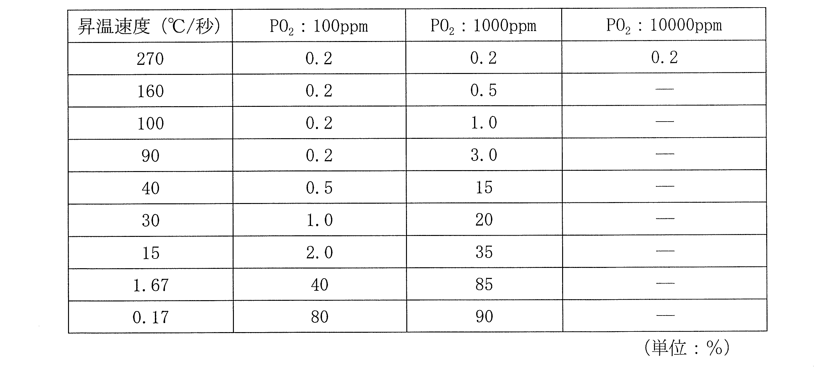
表4における「PO2:10000ppm」の欄において数値が記入されていないものについては評価を行なわなかった。すなわち、酸素分圧が10000ppmの条件下では、昇温速度270℃/秒についてのみ評価した。 Evaluation was not performed for those for which no numerical value was entered in the column “PO 2 : 10000 ppm” in Table 4. That is, only the temperature increase rate of 270 ° C./second was evaluated under the condition where the oxygen partial pressure was 10,000 ppm.
表4および図11から、酸素分圧100ppmにおいて、昇温速度が40℃/秒以上であれば、電極酸化度1%以下でNi内部電極を備える積層セラミックコンデンサの焼成が可能であることがわかる。さらに、昇温速度を100℃/秒以上とすることにより、酸素分圧1000ppmにおいても、電極酸化度1%以下で焼成が可能であることがわかる。また、酸素分圧10000ppmと高くても、この実験例では、昇温速度を270℃/秒とすることにより、0.2%の電極酸化度と抑制できることがわかる。 From Table 4 and FIG. 11, it can be seen that if the rate of temperature rise is 40 ° C./second or higher at an oxygen partial pressure of 100 ppm, it is possible to fire a multilayer ceramic capacitor having a Ni internal electrode with an electrode oxidation degree of 1% or less. . Furthermore, it can be seen that by setting the rate of temperature rise to 100 ° C./second or more, firing can be performed with an electrode oxidation degree of 1% or less even at an oxygen partial pressure of 1000 ppm. Moreover, even if the oxygen partial pressure is as high as 10,000 ppm, it can be seen that in this experimental example, the electrode oxidation degree of 0.2% can be suppressed by setting the temperature rising rate to 270 ° C./second.
これらの結果から、昇温速度を高めることにより、焼成時の酸素分圧が相対的に高くなるので、セラミック還元(酸素空孔の生成)が抑制され、得られた積層セラミックコンデンサの信頼性が向上するといった効果が得られることがわかる。 From these results, since the oxygen partial pressure during firing becomes relatively high by increasing the temperature rising rate, ceramic reduction (generation of oxygen vacancies) is suppressed, and the reliability of the obtained multilayer ceramic capacitor is improved. It turns out that the effect of improving is acquired.
6.実験例6(大グレイン領域と小グレイン領域との境界面の影響)
実験例6では、通常の直方体形状を持つ積層セラミックコンデンサについて、試料1~4をそれぞれ作製し、かつ評価した。試料1~4の概略を述べると、次のとおりである。試料1は、この発明の範囲内の実施例であり、LW面およびLT面の各々の内側に境界面が存在するものである。他方、試料2~4は、この発明の範囲外の比較例である。特に、試料2は、LW面の内側にのみ境界面が存在するもの、試料3は、LT面の内側にのみ境界面が存在するもの、試料4は、いずれにも境界面が存在しないものである。
6). Experimental Example 6 (Influence of boundary surface between large grain region and small grain region)
In Experimental Example 6,
(1)セラミック原料粉末の作製
<比較的小径のセラミック原料粉末A>
BaCO3粉末とTiO2粉末とを、Ba/Tiモル比が1.001になるように秤量して、ZrO2ボールを用いたミルにて湿式混合粉砕した。湿式粉砕で得たスラリーを乾燥後、900℃以上に加熱し、平均粒子径が0.2μmのBaTiO3粉末を作製した。このBaTiO3粉末100モル部に対し、0.5モル部のDy2O3粉末、1.2モル部のMgCO3粉末、0.2モル部のMnCO3粉末、および1.0モル部のBaCO3粉末をそれぞれ添加し、さらにSiO2換算で1.2モル部のSiO2ゾルを添加して、ZrO2ボールを使ったミルにより湿式混合粉砕を行ない、その後、湿式混合粉砕で得たスラリーを乾燥し、セラミック原料粉末Aを作製した。
(1) Production of ceramic raw material powder <Relatively small diameter ceramic raw material powder A>
BaCO 3 powder and TiO 2 powder were weighed so that the Ba / Ti molar ratio was 1.001, and wet-mixed and pulverized in a mill using ZrO 2 balls. The slurry obtained by wet pulverization was dried and then heated to 900 ° C. or higher to prepare BaTiO 3 powder having an average particle size of 0.2 μm. For 100 mol parts of this BaTiO 3 powder, 0.5 mol parts of Dy 2 O 3 powder, 1.2 mol parts of MgCO 3 powder, 0.2 mol parts of MnCO 3 powder, and 1.0 mol parts of BaCO. 3 powders were added, and 1.2 mol part of SiO 2 sol was added in terms of SiO 2 , and wet mixing and pulverization was performed by a mill using ZrO 2 balls. It dried and produced ceramic raw material powder A.
<比較的大径のセラミック原料粉末B>
BaCO3粉末とTiO2粉末とを、Ba/Tiモル比が1.001になるように秤量して、ZrO2ボールを用いたミルにて湿式混合粉砕した。湿式粉砕で得たスラリーを乾燥後、1000℃以上に加熱し、平均粒子径が0.5μmのBaTiO3粉末を作製した。このBaTiO3粉末100モル部に対し、0.25モル部のDy2O3粉末、1.2モル部のMgCO3粉末、0.2モル部のMnCO3粉末、および1.0モル部のBaCO3粉末をそれぞれ添加し、さらにSiO2換算で1.7モル部のSiO2ゾルを添加して、ZrO2ボールを使ったミルにより湿式混合粉砕を行ない、その後、湿式混合粉砕で得たスラリーを乾燥し、セラミック原料粉末Bを作製した。
<Relatively large diameter ceramic raw material powder B>
BaCO 3 powder and TiO 2 powder were weighed so that the Ba / Ti molar ratio was 1.001, and wet-mixed and pulverized in a mill using ZrO 2 balls. After drying the slurry obtained by wet milling, heated above 1000 ° C., an average particle diameter were produced BaTiO 3 powder of 0.5 [mu] m. For 100 mol parts of this BaTiO 3 powder, 0.25 mol parts of Dy 2 O 3 powder, 1.2 mol parts of MgCO 3 powder, 0.2 mol parts of MnCO 3 powder, and 1.0 mol parts of BaCO. 3 powders were added, and 1.7 mol parts of SiO 2 sol was added in terms of SiO 2 , and wet mixing and pulverization were performed by a mill using ZrO 2 balls. It dried and produced ceramic raw material powder B.
(2)セラミックスラリーおよびセラミックグリーンシートの作製
セラミック原料粉末Aに、ポリブチラール系バインダと可塑剤とを添加し、エチルアルコール類を加えて、ZrO2ボールミルにより湿式混合粉砕してスラリー化し、グラビアコーターで厚みが2.8μmのセラミックグリーンシートAを成形した。
(2) Production of ceramic slurry and ceramic green sheet To the ceramic raw material powder A, a polybutyral binder and a plasticizer are added, ethyl alcohols are added, and wet blended and pulverized with a ZrO 2 ball mill to form a slurry, and a gravure coater A ceramic green sheet A having a thickness of 2.8 μm was formed.
セラミック原料粉末Bについても、同様な方法で、厚みが5μmのセラミックグリーンシートBを成形した。 For the ceramic raw material powder B, a ceramic green sheet B having a thickness of 5 μm was formed by the same method.
また、セラミックグリーンシートBを成形するために調製したスラリーを一部分取し、溶剤を部分除去することによって、増粘させたセラミックススラリーCを作製した。 Further, a portion of the slurry prepared for forming the ceramic green sheet B was taken, and the solvent was partially removed to prepare a thickened ceramic slurry C.
(3)積層体の作製
<試料1>
セラミックグリーンシートA上に、ニッケルを主成分とする導電性ペーストをスクリーン印刷し、内部電極となる導電性ペースト膜パターンを形成した。その後、導電性ペースト膜が形成されたセラミックグリーンシートAを、導電性ペースト膜の引き出されている側が互い違いになるように280枚積層して内層部とし、さらに、この内層部を挟み込む外層部を形成するため、導電性ペースト膜を形成していないセラミックグリーンシートAを積層した。片側の外層部の厚みは145μmであった。次に、このようにして得られたグリーン積層ブロックAに対してダイシングソーを適用して、片側のサイドギャップ部の厚さが145μmになるようにグリーン積層ブロックAをカットし、多数のグリーン積層チップAを得た。
(3) Production of laminate <
On the ceramic green sheet A, the conductive paste which has nickel as a main component was screen-printed, and the conductive paste film pattern used as an internal electrode was formed. Thereafter, 280 ceramic green sheets A on which the conductive paste film is formed are stacked so that the side from which the conductive paste film is drawn is alternated to form an inner layer portion, and an outer layer portion sandwiching the inner layer portion is further formed. In order to form, the ceramic green sheet A in which the conductive paste film was not formed was laminated. The thickness of the outer layer part on one side was 145 μm. Next, a dicing saw is applied to the green laminated block A thus obtained, and the green laminated block A is cut so that the thickness of the side gap portion on one side becomes 145 μm. Chip A was obtained.
<試料2>
セラミックグリーンシートA上に、ニッケルを主成分とする導電性ペーストをスクリーン印刷し、内部電極となる導電性ペースト膜パターンを形成した。その後、導電性ペースト膜が形成されたセラミックグリーンシートAを、導電性ペースト膜の引き出されている側が互い違いになるように280枚積層して内層部とし、さらに、この内層部を挟み込む外層部を形成するため、導電性ペースト膜を形成していないセラミックグリーンシートBを積層した。片側の外層部の厚みは145μmであった。次に、このようにして得られたグリーン積層ブロックBに対してダイシングソーを適用して、片側のサイドギャップ部の厚さが145μmになるようにグリーン積層ブロックBをカットし、多数のグリーン積層チップBを得た。
<
On the ceramic green sheet A, the conductive paste which has nickel as a main component was screen-printed, and the conductive paste film pattern used as an internal electrode was formed. Thereafter, 280 ceramic green sheets A on which the conductive paste film is formed are stacked so that the side from which the conductive paste film is drawn is alternated to form an inner layer portion, and an outer layer portion sandwiching the inner layer portion is further formed. In order to form, the ceramic green sheet B in which the conductive paste film was not formed was laminated. The thickness of the outer layer part on one side was 145 μm. Next, a dicing saw is applied to the green laminated block B thus obtained, and the green laminated block B is cut so that the thickness of the side gap portion on one side becomes 145 μm. Chip B was obtained.
<試料3>
セラミックグリーンシートA上に、ニッケルを主成分とする導電性ペーストをスクリーン印刷し、内部電極となる導電性ペースト膜パターンを形成した。その後、導電性ペースト膜が形成されたセラミックグリーンシートAを、導電性ペースト膜の引き出されている側が互い違いになるように280枚積層して内層部とし、さらに、この内層部を挟み込む外層部を形成するため、導電性ペースト膜を形成していないセラミックグリーンシートAを積層した。片側の外層部の厚みは145μmであった。次に、このようにして得られたグリーン積層ブロックCに対してダイシングソーを適用して、片側のサイドギャップの厚さが10μmになるようにグリーン積層ブロックCをカットした。次に、このように切り分けた個片のLT面となるべき表面に、セラミックススラリーCを、所定の厚み分だけ塗布し、乾燥させ、サイドギャップの厚みを片側で145μmとした。さらにカットを進め、グリーン積層チップCを得た。
<
On the ceramic green sheet A, the conductive paste which has nickel as a main component was screen-printed, and the conductive paste film pattern used as an internal electrode was formed. Thereafter, 280 ceramic green sheets A on which the conductive paste film is formed are stacked so that the side from which the conductive paste film is drawn is alternated to form an inner layer portion, and an outer layer portion sandwiching the inner layer portion is further formed. In order to form, the ceramic green sheet A in which the conductive paste film was not formed was laminated. The thickness of the outer layer part on one side was 145 μm. Next, a dicing saw was applied to the green laminated block C thus obtained, and the green laminated block C was cut so that the thickness of the side gap on one side was 10 μm. Next, the ceramic slurry C was applied by a predetermined thickness on the surface to be the LT surface of the individual piece thus cut, and dried to set the side gap thickness to 145 μm on one side. Further cutting was performed to obtain a green laminated chip C.
<試料4>
試料1の場合と同じ工程を適用して、多数のグリーン積層チップDを得た。なお、グリーン積層チップDは、前述のグリーン積層チップAと同じ性状を有するものである。
<
The same process as in the case of
(4)積層セラミックコンデンサの作製
上記のように作製したグリーン積層チップA~Dを、N2気流中、280℃で熱処理し、バインダを燃焼除去した。引き続き、これらを、N2/H2/H2O気流中、酸素分圧:10-9.6MPaの雰囲気下で焼成した。
(4) Production of Multilayer Ceramic Capacitor The green multilayer chips A to D produced as described above were heat-treated at 280 ° C. in a N 2 gas stream to burn and remove the binder. Subsequently, these were fired in an N 2 / H 2 / H 2 O stream under an atmosphere having an oxygen partial pressure of 10 −9.6 MPa.
ここで、表5に示すように、試料1に係るグリーン積層チップAについては、平均昇温速度を40℃/秒、最高温度1300℃、最高温度保持時間1秒間の加熱条件で焼成した。
Here, as shown in Table 5, the green laminated chip A according to
また、試料2、3および4の各々に係るグリーン積層チップB、CおよびDについては、平均昇温速度0.17℃/秒、最高温度1220℃、最高温度保持時間1時間の加熱条件で焼成した。
In addition, green laminated chips B, C, and D relating to each of

次に、上記のように焼成して得られた積層チップにおける、内部電極が引き出された端面部に外部電極を形成するため、Cuを主成分とする導電性ペーストを塗布して、800℃の温度で焼き付けることにより、Cu厚膜層を形成し、さらに、Cu厚膜層上に、NiめっきおよびSnめっきを施した。 Next, in order to form an external electrode on the end face part from which the internal electrode was drawn out in the laminated chip obtained by firing as described above, a conductive paste containing Cu as a main component was applied, and the 800 ° C. By baking at a temperature, a Cu thick film layer was formed, and Ni plating and Sn plating were further performed on the Cu thick film layer.
このようにして得られた積層セラミックコンデンサの寸法(外部電極を含む寸法)は、長さL:2.0mm、幅W:1.2mm、厚みT:1.2mmであった。また、誘電体セラミック層の1層あたりの厚みは2.0μmであった。また、内部電極の重なり部の面積は2.0mm2であった。また、外層部の厚みは120μm、サイドギャップ部の厚みは120μmであった。 The dimensions of the multilayer ceramic capacitor thus obtained (including the external electrodes) were length L: 2.0 mm, width W: 1.2 mm, and thickness T: 1.2 mm. The thickness of the dielectric ceramic layer per layer was 2.0 μm. The area of the overlapping part of the internal electrodes was 2.0 mm 2 . The thickness of the outer layer portion was 120 μm, and the thickness of the side gap portion was 120 μm.
(5)評価
試料1に係る積層セラミックコンデンサの積層体のLT面に平行な断面を観察したところ、外層部における、最も外側の内部電極から約45μmの距離に、その内外でグレイン径分布の互いに異なる境界面が観察された。同様に、積層体のLW面に平行な断面を観察したところ、サイドギャップ部における、内部電極の側縁から約45μmの距離にも、同様の境界面が観察された。
(5) Evaluation When a cross section parallel to the LT surface of the multilayer ceramic capacitor multilayer body according to
図12は、試料1に係る積層セラミックコンデンサの積層体のLT面に平行な断面を撮像したSEM像を示している。図12の上端は、最も外側の内部電極から60μmの距離にあり、図12の下端は、最も外側の内部電極から25μmの距離にある。図12において、境界面の内外でグレイン径分布が互いに異なっている様子が観察される。
FIG. 12 shows an SEM image obtained by imaging a cross section parallel to the LT surface of the multilayer ceramic capacitor multilayer body according to
他方、試料2では、外層部のみに境界面が観察され、試料3では、サイドギャップ部のみに境界面が観察された。また、試料4では、いずれにも境界面が観察されなかった。
On the other hand, in
次に、各試料に係る積層セラミックコンデンサを破断し、N2/H2気流中、1000℃の温度下で5分間、サーマル・エッチングを実施した後、破断面を30000倍で撮影したSEM写真を画像解析し、各グレインの面積等価円相当径を、グレイン径として算出することによって、外層部およびサイドギャップ部の各々における、内部電極からの距離が20~40μmの領域にあるグレインのグレイン径、および、内部電極からの距離が50μm~70μmの領域にあるグレインのグレイン径を求めた。 Next, after breaking the multilayer ceramic capacitor according to each sample and performing thermal etching for 5 minutes at a temperature of 1000 ° C. in a N 2 / H 2 airflow, SEM photographs were taken of the fractured surface at 30000 times. By analyzing the image and calculating the area equivalent circle equivalent diameter of each grain as the grain diameter, the grain diameter of the grains in the region whose distance from the internal electrode is 20 to 40 μm in each of the outer layer portion and the side gap portion, In addition, the grain diameter of the grains in the region where the distance from the internal electrode is 50 μm to 70 μm was determined.
上記画像解析は、1視野あたりの面積が12.5μm2のSEM写真、50視野分について行ない、グレイン径を求めた。そして、各視野において、グレイン径の小さな順に並べて、各グレインの面積の累計が、視野全体の80%に達した順位のグレイン径を、その視野におけるグレイン径分布のD80値と定義した。 The image analysis was performed on SEM photographs having an area per visual field of 12.5 μm 2 and 50 visual fields, and the grain diameter was determined. In each field of view, are arranged in ascending order of the grain diameter, total area of each grain, the grain diameter of the order reaching 80% of the entire field of view was defined as the 80 value D of the grain size distribution in its field of view.
そして、外層部およびサイドギャップ部の各々について、内部電極からの距離が20~40μmの領域がたとえば試料1では境界面内側の領域に相当するが、この領域でのD80値のうち、最大の値を、表6において、「20~40μm領域の最大D80値」として示した。また、内部電極からの距離が50~70μmの領域がたとえば試料1では境界面外側の領域に相当するが、この領域でのD80値のうち、最小の値を、表6において、「50~70μm領域の最小D80値」として示した。
For each of the outer layer portion and the side gap portion, a region having a distance of 20 to 40 μm from the internal electrode corresponds to a region on the inner side of the boundary surface in the

表6には、前述した境界面の有無についても示されている。 Table 6 also shows the presence or absence of the boundary surface described above.
表6に示すように、境界面が存在しない外層部またはサイドギャップ部では、当然のことながら、「20~40μm領域の最大D80値」と「50~70μm領域の最小D80値」とが同じ値を示している。これに対して、境界面が存在する外層部またはサイドギャップ部では、「20~40μm領域の最大D80値」に比べて、「50~70μm領域の最小D80値」が大きい値を示し、後者の「50~70μm領域の最小D80値」は、前者の「20~40μm領域の最大D80値」の5倍以上の値を示した。 As shown in Table 6, in the outer layer portion or the side gap portion where the boundary surface does not exist, the “maximum D 80 value in the 20 to 40 μm region” and the “minimum D 80 value in the 50 to 70 μm region” are naturally It shows the same value. On the other hand, in the outer layer portion or the side gap portion where the boundary surface exists, the “minimum D 80 value in the 50 to 70 μm region” is larger than the “maximum D 80 value in the 20 to 40 μm region”. The latter “minimum D 80 value in the 50 to 70 μm region” was 5 times or more than the former “maximum D 80 value in the 20 to 40 μm region”.
他方、各試料に係る積層セラミックコンデンサの、直流電圧を印加しない場合の静電容量(CDC0V)を、自動ブリッジ式測定器を用い、120Hz、1.0Vの条件下で、温度25℃において測定した。 On the other hand, the capacitance (C DC0V ) of the multilayer ceramic capacitor according to each sample when no DC voltage is applied is measured at a temperature of 25 ° C. under the conditions of 120 Hz and 1.0 V using an automatic bridge type measuring instrument. did.
次に、同様の要領にて、直流電圧印加下での静電容量を、直流電圧4Vを1秒間印加した時点での静電容量(CDC4V)として求めた。 Next, in the same manner, the capacitance under application of a DC voltage was determined as the capacitance (C DC4V ) when a DC voltage of 4 V was applied for 1 second.
なお、静電容量を測定する24時間前には、150℃の温度にて1時間、測定する積層セラミックコンデンサの試料を加熱し、加熱後から測定するまで、25℃の温度下にて電圧を印加せずに保管する処理を行なった。 In addition, 24 hours before measuring the capacitance, the sample of the multilayer ceramic capacitor to be measured was heated at a temperature of 150 ° C. for 1 hour, and the voltage was applied at a temperature of 25 ° C. until the measurement was performed after the heating. The process which stored without applying is performed.
前述した方法で測定した静電容量(CDC0VおよびCDC4V)と、誘電体セラミック層厚み、内部電極重なり面積、および積層数とから、表7に示すように、各試料に係るセラミックコンデンサにおける、直流電圧を印加しない場合の基準の誘電率(εDC0V)と直流電圧下での誘電率(εDC4V)とを求めるとともに、基準の誘電率(εDC0V)および直流電圧下での誘電率(εDC4V)から、基準の誘電率(εDC0V)に対する、直流電圧下での誘電率(εDC4V)の変化率、すなわち誘電率変化率(Δε)[%]を、Δε={(εDC4V-εDC0V)/εDC0V}×100の式により算出した。 The capacitance measured in the above-described method (C 0V dc and C DC4V), dielectric ceramic layer thickness, the area overlapping the internal electrodes, and the number of laminated layers, as shown in Table 7, in the ceramic capacitor according to each sample, reference dielectric constant when no DC voltage was applied (epsilon 0V dc) and the dielectric constant under a DC voltage (ε DC4V) and with obtaining the reference dielectric constant (epsilon 0V dc) and DC dielectric constant under voltage (epsilon from DC4V), reference dielectric constant with respect to (epsilon 0V dc), the dielectric constant under a DC voltage (ε DC4V) rate of change, ie the dielectric constant change rate (Δε) [%], Δε = {(ε DC4V -ε DC0V ) / εDC0V } × 100.

表7からわかるように、試料1において、最も高い誘電率を示した。そして、試料1によれば、基準の誘電率(εDC0V)が高いにも関わらず、他の試料2~4に比べて、直流電圧下での誘電率(εDC4V)があまり低下しておらず、誘電率変化率(Δε)が小さかった。
As can be seen from Table 7,
このような表7に示した結果と前述した表6に示した結果とを併せて考察すると、次のことがわる。 Considering the results shown in Table 7 together with the results shown in Table 6 described above, the following can be seen.
試料1によれば、表7に示すように、誘電率変化率(Δε)が小さい。他方、表6に示すように、試料1では、境界面が外層部およびサイドギャップ部の双方において存在し、かつ「20~40μm領域の最大D80値」に比べて「50~70μm領域の最小D80値」が大きい値を示している。このことから、試料1のように、大グレイン領域が小グレイン領域の外側に位置し、かつ大グレイン領域とグレイン領域との境界面が、内部電極の存在する部分の外側であって、外層部およびサイドギャップ部に沿って延びるように積層体の外表面の内側に位置していると、セラミック層が薄層化されても、DCバイアス特性を良好に維持できることがわかる。
According to
そして、上述したような試料1が有する特徴的なグレイン径分布を有利に実現するには、焼成工程において、室温から最高温度までの平均昇温速度を40℃/秒以上とする温度プロファイルにて熱処理する工程を採用することが有効であることがわかる。
In order to advantageously realize the characteristic grain size distribution of the
これに対して、内部電極の存在する部分が境界面によって部分的にしか覆われていない場合、すなわち、試料2のように境界面が外層部のみに存在する場合、または試料3のように境界面がサイドギャップ部のみに存在する場合、さらには、試料4のように境界面がいずれにも存在しない場合には、誘電率変化率が大きくなり、DCバイアス特性が劣ることがわかる。
On the other hand, when the portion where the internal electrode exists is only partially covered by the boundary surface, that is, when the boundary surface exists only in the outer layer portion as in the
1 積層セラミックコンデンサ
2,12 積層体
3 セラミック層
4,5 内部電極
8,9 外部電極
13 大グレイン領域
14 小グレイン領域
15 境界面
16 素子部分
DESCRIPTION OF
Claims (8)
特定の前記内部電極と電気的に接続されるように前記積層体の外表面上に形成される外部電極と
を備え、
前記積層体は、前記セラミック層を構成するセラミックのグレイン径に関して、これが比較的大きい大グレイン領域と比較的小さい小グレイン領域とに分類され、前記大グレイン領域は前記小グレイン領域の外側に位置し、前記大グレイン領域と前記小グレイン領域との境界面は、前記積層体における前記内部電極の存在する部分を囲みながら前記積層体の外表面の内側に位置している、
積層セラミック電子部品。 A laminate comprising a plurality of laminated ceramic layers and internal electrodes formed along specific interfaces between the ceramic layers;
An external electrode formed on the outer surface of the laminate so as to be electrically connected to the specific internal electrode,
The laminated body is classified into a large grain region having a relatively large size and a small grain region having a relatively small size with respect to a diameter of a ceramic constituting the ceramic layer, and the large grain region is located outside the small grain region. The boundary surface between the large grain region and the small grain region is located inside the outer surface of the stacked body while surrounding the portion where the internal electrode exists in the stacked body,
Multilayer ceramic electronic components.
特定の前記内部電極と電気的に接続されるように前記積層体の外表面上に形成される外部電極と
を備え、
前記積層体は、その長さ方向寸法Lおよびその幅方向寸法Wによって規定されるLW面と、その長さ方向寸法Lおよびその厚み方向寸法Tによって規定されるLT面と、その幅方向寸法Wおよびその厚み方向寸法Tによって規定されるWT面とを有する直方体形状であり、
前記外部電極は前記WT面上に形成され、
前記積層体は、前記セラミック層を構成するセラミックのグレイン径に関して、これが比較的大きい大グレイン領域と比較的小さい小グレイン領域とに分類され、前記大グレイン領域は前記小グレイン領域の外側に位置し、前記大グレイン領域と前記小グレイン領域との境界面は、前記積層体における前記内部電極の存在する部分の外側であって、少なくとも前記LW面および前記LT面に沿って連続的に延びるように前記積層体の外表面の内側に位置している、
積層セラミック電子部品。 A laminate comprising a plurality of laminated ceramic layers and internal electrodes formed along specific interfaces between the ceramic layers;
An external electrode formed on the outer surface of the laminate so as to be electrically connected to the specific internal electrode,
The laminate has an LW surface defined by its lengthwise dimension L and its widthwise dimension W, an LT surface defined by its lengthwise dimension L and its thicknesswise dimension T, and its widthwise dimension W. And a cuboid shape having a WT surface defined by a thickness direction dimension T thereof,
The external electrode is formed on the WT surface,
The laminated body is classified into a large grain region having a relatively large size and a small grain region having a relatively small size with respect to a diameter of a ceramic constituting the ceramic layer, and the large grain region is located outside the small grain region. The boundary surface between the large grain region and the small grain region is outside the portion where the internal electrode is present in the multilayer body, and extends continuously along at least the LW surface and the LT surface. Located inside the outer surface of the laminate,
Multilayer ceramic electronic components.
前記生の積層体を焼結させるため、焼成する工程と
を備え、
前記焼成する工程は、室温から最高温度までの平均昇温速度を40℃/秒以上とする温度プロファイルにて熱処理する工程を備える、積層セラミック電子部品の製造方法。 Providing a raw laminate comprising a plurality of laminated ceramic layers and internal electrodes formed along a specific interface between the ceramic layers;
In order to sinter the raw laminate, it comprises a firing step,
The step of firing includes a step of heat-treating with a temperature profile in which an average rate of temperature rise from room temperature to a maximum temperature is 40 ° C./second or more, and a method for manufacturing a multilayer ceramic electronic component.
Priority Applications (5)
| Application Number | Priority Date | Filing Date | Title |
|---|---|---|---|
| JP2010543339A JP5287869B2 (en) | 2009-06-15 | 2010-05-21 | Multilayer ceramic electronic component and manufacturing method thereof |
| KR1020117000219A KR101143128B1 (en) | 2009-06-15 | 2010-05-21 | Laminated ceramic electronic component and manufacturing method therefor |
| CN201080002124.3A CN102099880B (en) | 2009-06-15 | 2010-05-21 | Laminated ceramic electronic component and manufacturing method therefor |
| US13/004,213 US8540832B2 (en) | 2009-06-15 | 2011-01-11 | Laminated ceramic electronic component and manufacturing method therefor |
| US13/956,616 US9183986B2 (en) | 2009-06-15 | 2013-08-01 | Laminated ceramic electronic component and manufacturing method therefor |
Applications Claiming Priority (4)
| Application Number | Priority Date | Filing Date | Title |
|---|---|---|---|
| JP2009-141866 | 2009-06-15 | ||
| JP2009141866 | 2009-06-15 | ||
| JP2009156655 | 2009-07-01 | ||
| JP2009-156655 | 2009-07-01 |
Related Child Applications (1)
| Application Number | Title | Priority Date | Filing Date |
|---|---|---|---|
| US13/004,213 Continuation US8540832B2 (en) | 2009-06-15 | 2011-01-11 | Laminated ceramic electronic component and manufacturing method therefor |
Publications (1)
| Publication Number | Publication Date |
|---|---|
| WO2010146967A1 true WO2010146967A1 (en) | 2010-12-23 |
Family
ID=43356288
Family Applications (1)
| Application Number | Title | Priority Date | Filing Date |
|---|---|---|---|
| PCT/JP2010/058618 Ceased WO2010146967A1 (en) | 2009-06-15 | 2010-05-21 | Laminated ceramic electronic component and manufacturing method therefor |
Country Status (6)
| Country | Link |
|---|---|
| US (2) | US8540832B2 (en) |
| JP (1) | JP5287869B2 (en) |
| KR (1) | KR101143128B1 (en) |
| CN (1) | CN102099880B (en) |
| TW (1) | TWI424455B (en) |
| WO (1) | WO2010146967A1 (en) |
Cited By (14)
| Publication number | Priority date | Publication date | Assignee | Title |
|---|---|---|---|---|
| WO2012111592A1 (en) * | 2011-02-14 | 2012-08-23 | 株式会社村田製作所 | Multilayer ceramic capacitor and multilayer ceramic capacitor manufacturing method |
| JP2013055333A (en) * | 2011-08-31 | 2013-03-21 | Samsung Electro-Mechanics Co Ltd | Magnetic substrate and method for manufacturing the same |
| JP2013157459A (en) * | 2012-01-30 | 2013-08-15 | Tdk Corp | Laminated ceramic capacitor |
| US20130222973A1 (en) * | 2010-11-24 | 2013-08-29 | Murata Manufacturing Co., Ltd. | Laminated Ceramic Electronic Component and Manufacturing Method Therefor |
| JP5298255B1 (en) * | 2012-06-19 | 2013-09-25 | 太陽誘電株式会社 | Multilayer ceramic capacitor |
| JP2013229546A (en) * | 2012-04-26 | 2013-11-07 | Samsung Electro-Mechanics Co Ltd | Multilayer ceramic electronic component and manufacturing method thereof |
| JP2014082462A (en) * | 2012-09-27 | 2014-05-08 | Taiyo Yuden Co Ltd | Multilayer ceramic capacitor |
| JP2014093515A (en) * | 2012-11-06 | 2014-05-19 | Samsung Electro-Mechanics Co Ltd | Multilayered ceramic electronic component |
| JPWO2013175945A1 (en) * | 2012-05-24 | 2016-01-12 | 株式会社村田製作所 | Multilayer ceramic electronic components |
| JP2018098489A (en) * | 2016-12-14 | 2018-06-21 | サムソン エレクトロ−メカニックス カンパニーリミテッド. | Inductor |
| JP2018142728A (en) * | 2016-02-18 | 2018-09-13 | 太陽誘電株式会社 | Multilayer ceramic capacitor |
| JP2019029422A (en) * | 2017-07-26 | 2019-02-21 | 太陽誘電株式会社 | Multilayer ceramic capacitor and manufacturing method thereof |
| JP2022104550A (en) * | 2020-12-28 | 2022-07-08 | サムソン エレクトロ-メカニックス カンパニーリミテッド. | Laminated capacitor and mounting substrate for the same |
| WO2025164016A1 (en) * | 2024-02-01 | 2025-08-07 | 株式会社村田製作所 | Multilayer ceramic capacitor |
Families Citing this family (25)
| Publication number | Priority date | Publication date | Assignee | Title |
|---|---|---|---|---|
| CN102473523B (en) * | 2009-08-20 | 2014-07-23 | 株式会社村田制作所 | Manufacturing method of laminated ceramic capacitor, and laminated ceramic capacitor |
| WO2013021885A1 (en) * | 2011-08-05 | 2013-02-14 | 株式会社村田製作所 | Method of manufacturing ceramic electronic part |
| JP5556854B2 (en) * | 2012-06-12 | 2014-07-23 | 株式会社村田製作所 | Method for manufacturing ceramic electronic component and ceramic electronic component |
| KR101983130B1 (en) | 2012-09-06 | 2019-05-28 | 삼성전기주식회사 | Multi-layered ceramic capacitor and manufacturing method thereof |
| JP2015126219A (en) * | 2013-12-27 | 2015-07-06 | 株式会社村田製作所 | Multilayer ceramic capacitor |
| JP2015126220A (en) * | 2013-12-27 | 2015-07-06 | 株式会社村田製作所 | Multilayer ceramic capacitor |
| JP6439551B2 (en) * | 2014-05-21 | 2018-12-19 | 株式会社村田製作所 | Multilayer ceramic capacitor |
| JP6665438B2 (en) * | 2015-07-17 | 2020-03-13 | 株式会社村田製作所 | Multilayer ceramic capacitors |
| JP6793027B2 (en) * | 2016-12-16 | 2020-12-02 | 太陽誘電株式会社 | Multilayer ceramic electronic components |
| JP6888324B2 (en) * | 2017-02-23 | 2021-06-16 | 株式会社村田製作所 | Manufacturing method of multilayer ceramic electronic components |
| JP2020167283A (en) | 2019-03-29 | 2020-10-08 | 株式会社村田製作所 | Multilayer ceramic capacitors |
| KR102257992B1 (en) * | 2019-07-08 | 2021-05-28 | 삼성전기주식회사 | Capacitor component |
| KR102333094B1 (en) * | 2019-07-08 | 2021-12-01 | 삼성전기주식회사 | Capacitor component |
| JP2021034648A (en) * | 2019-08-28 | 2021-03-01 | 株式会社村田製作所 | Multilayer ceramic capacitor |
| CN114502904A (en) * | 2020-02-20 | 2022-05-13 | 日本碍子株式会社 | Dielectric drying method and dielectric drying device for ceramic molded body, and method for manufacturing ceramic structure |
| JP7821569B2 (en) * | 2020-12-16 | 2026-02-27 | 太陽誘電株式会社 | Multilayer ceramic capacitor and method of manufacturing the same |
| JP7750662B2 (en) * | 2021-03-17 | 2025-10-07 | 太陽誘電株式会社 | Ceramic electronic component and manufacturing method thereof |
| US11990284B2 (en) * | 2021-05-25 | 2024-05-21 | Samsung Electro-Mechanics Co., Ltd. | Multilayered electronic component |
| US12051543B2 (en) * | 2021-05-25 | 2024-07-30 | Samsung Electro-Mechanics Co., Ltd. | Mutilayer electronic component and method of manufacturing the same |
| JP2023057491A (en) * | 2021-10-11 | 2023-04-21 | 株式会社村田製作所 | Multilayer ceramic capacitor |
| KR102946060B1 (en) * | 2021-12-29 | 2026-04-01 | 삼성전기주식회사 | Mutilayered electronic component |
| WO2023223652A1 (en) * | 2022-05-20 | 2023-11-23 | 株式会社村田製作所 | Multilayer ceramic capacitor |
| KR20250002660A (en) * | 2022-06-03 | 2025-01-07 | 가부시키가이샤 무라타 세이사쿠쇼 | Multilayer Ceramic Capacitor |
| CN119054034A (en) * | 2022-06-08 | 2024-11-29 | 株式会社村田制作所 | Laminated ceramic capacitor |
| JP2025139421A (en) * | 2024-03-12 | 2025-09-26 | 株式会社村田製作所 | Multilayer ceramic capacitors |
Citations (6)
| Publication number | Priority date | Publication date | Assignee | Title |
|---|---|---|---|---|
| JPH06267785A (en) * | 1993-03-12 | 1994-09-22 | Toshiba Corp | Method for manufacturing monolithic ceramic electronic component |
| JPH10149941A (en) * | 1996-11-18 | 1998-06-02 | Toyota Central Res & Dev Lab Inc | Method for manufacturing multilayer substrate |
| JPH10241987A (en) * | 1997-02-25 | 1998-09-11 | Tokin Corp | Manufacturing method of multilayer ceramic capacitor |
| JP2002289457A (en) * | 2001-03-28 | 2002-10-04 | Kyocera Corp | Manufacturing method of multilayer ceramic electronic component |
| KR20060135249A (en) * | 2005-06-24 | 2006-12-29 | 삼성전기주식회사 | High Speed Heating Firing Method of Laminated Chips |
| JP2008226941A (en) * | 2007-03-09 | 2008-09-25 | Matsushita Electric Ind Co Ltd | Manufacturing method of ceramic capacitor |
Family Cites Families (15)
| Publication number | Priority date | Publication date | Assignee | Title |
|---|---|---|---|---|
| US4039338A (en) * | 1972-12-29 | 1977-08-02 | International Business Machines Corporation | Accelerated sintering for a green ceramic sheet |
| US4490319A (en) * | 1983-10-26 | 1984-12-25 | General Electric Company | Rapid rate sintering of ceramics |
| US5260094A (en) * | 1991-09-30 | 1993-11-09 | Cornell Research Foundation, Inc. | Preparing densified low porosity titania sol-gel forms |
| US5391339A (en) * | 1992-12-31 | 1995-02-21 | Valenite Inc. | Continuous process for producing alumina-titanium carbide composites |
| JPH08264721A (en) * | 1995-03-28 | 1996-10-11 | Olympus Optical Co Ltd | Dielectric capacitor |
| JPH11163273A (en) * | 1997-12-01 | 1999-06-18 | Tokyo Ohka Kogyo Co Ltd | Manufacture of dielectric thin film and dielectric capacitor and dielectric memory |
| JP4803854B2 (en) | 1999-01-27 | 2011-10-26 | Tdk株式会社 | Manufacturing method of multilayer ceramic capacitor |
| JP4551991B2 (en) | 2000-06-27 | 2010-09-29 | ルネサスエレクトロニクス株式会社 | Plasma etching method and semiconductor device manufactured using the same |
| JP2001284341A (en) | 2001-02-22 | 2001-10-12 | Tokyo Electron Ltd | Heat treatment method |
| JP4407299B2 (en) * | 2004-01-30 | 2010-02-03 | Tdk株式会社 | Multilayer ceramic capacitor |
| JP4574267B2 (en) * | 2004-07-28 | 2010-11-04 | 京セラ株式会社 | Manufacturing method of multilayer electronic component and multilayer electronic component |
| JP2006165259A (en) | 2004-12-07 | 2006-06-22 | Kyocera Corp | Dielectric porcelain and multilayer electronic components |
| JP2007173480A (en) * | 2005-12-21 | 2007-07-05 | Tdk Corp | Laminated electronic component and its manufacturing method |
| JP5164463B2 (en) * | 2007-07-26 | 2013-03-21 | 太陽誘電株式会社 | Manufacturing method of multilayer ceramic capacitor and multilayer ceramic capacitor |
| CN102473523B (en) * | 2009-08-20 | 2014-07-23 | 株式会社村田制作所 | Manufacturing method of laminated ceramic capacitor, and laminated ceramic capacitor |
-
2010
- 2010-05-21 JP JP2010543339A patent/JP5287869B2/en active Active
- 2010-05-21 WO PCT/JP2010/058618 patent/WO2010146967A1/en not_active Ceased
- 2010-05-21 CN CN201080002124.3A patent/CN102099880B/en active Active
- 2010-05-21 KR KR1020117000219A patent/KR101143128B1/en active Active
- 2010-05-31 TW TW099117472A patent/TWI424455B/en active
-
2011
- 2011-01-11 US US13/004,213 patent/US8540832B2/en active Active
-
2013
- 2013-08-01 US US13/956,616 patent/US9183986B2/en active Active
Patent Citations (6)
| Publication number | Priority date | Publication date | Assignee | Title |
|---|---|---|---|---|
| JPH06267785A (en) * | 1993-03-12 | 1994-09-22 | Toshiba Corp | Method for manufacturing monolithic ceramic electronic component |
| JPH10149941A (en) * | 1996-11-18 | 1998-06-02 | Toyota Central Res & Dev Lab Inc | Method for manufacturing multilayer substrate |
| JPH10241987A (en) * | 1997-02-25 | 1998-09-11 | Tokin Corp | Manufacturing method of multilayer ceramic capacitor |
| JP2002289457A (en) * | 2001-03-28 | 2002-10-04 | Kyocera Corp | Manufacturing method of multilayer ceramic electronic component |
| KR20060135249A (en) * | 2005-06-24 | 2006-12-29 | 삼성전기주식회사 | High Speed Heating Firing Method of Laminated Chips |
| JP2008226941A (en) * | 2007-03-09 | 2008-09-25 | Matsushita Electric Ind Co Ltd | Manufacturing method of ceramic capacitor |
Cited By (26)
| Publication number | Priority date | Publication date | Assignee | Title |
|---|---|---|---|---|
| US20130222973A1 (en) * | 2010-11-24 | 2013-08-29 | Murata Manufacturing Co., Ltd. | Laminated Ceramic Electronic Component and Manufacturing Method Therefor |
| US9136058B2 (en) * | 2010-11-24 | 2015-09-15 | Murata Manufacturing Co., Ltd. | Laminated ceramic electronic component and manufacturing method therefor |
| US9099244B2 (en) | 2011-02-14 | 2015-08-04 | Murata Manufacturing Co., Ltd. | Multilayer ceramic capacitor and method for manufacturing multilayer ceramic capacitor |
| WO2012111592A1 (en) * | 2011-02-14 | 2012-08-23 | 株式会社村田製作所 | Multilayer ceramic capacitor and multilayer ceramic capacitor manufacturing method |
| JP5488725B2 (en) * | 2011-02-14 | 2014-05-14 | 株式会社村田製作所 | Manufacturing method of multilayer ceramic capacitor |
| JP2013055333A (en) * | 2011-08-31 | 2013-03-21 | Samsung Electro-Mechanics Co Ltd | Magnetic substrate and method for manufacturing the same |
| JP2013157459A (en) * | 2012-01-30 | 2013-08-15 | Tdk Corp | Laminated ceramic capacitor |
| KR101823160B1 (en) * | 2012-04-26 | 2018-01-29 | 삼성전기주식회사 | Laminated ceramic electronic parts and manufacturing method thereof |
| JP2013229546A (en) * | 2012-04-26 | 2013-11-07 | Samsung Electro-Mechanics Co Ltd | Multilayer ceramic electronic component and manufacturing method thereof |
| JPWO2013175945A1 (en) * | 2012-05-24 | 2016-01-12 | 株式会社村田製作所 | Multilayer ceramic electronic components |
| WO2013190718A1 (en) * | 2012-06-19 | 2013-12-27 | 太陽誘電株式会社 | Laminated ceramic capacitor |
| US9607766B2 (en) | 2012-06-19 | 2017-03-28 | Taiyo Yuden Co., Ltd. | Laminated ceramic capacitor |
| JP5298255B1 (en) * | 2012-06-19 | 2013-09-25 | 太陽誘電株式会社 | Multilayer ceramic capacitor |
| JP2014082462A (en) * | 2012-09-27 | 2014-05-08 | Taiyo Yuden Co Ltd | Multilayer ceramic capacitor |
| JP2014093515A (en) * | 2012-11-06 | 2014-05-19 | Samsung Electro-Mechanics Co Ltd | Multilayered ceramic electronic component |
| JP2022020816A (en) * | 2016-02-18 | 2022-02-01 | 太陽誘電株式会社 | Multilayer ceramic capacitor |
| JP2018142728A (en) * | 2016-02-18 | 2018-09-13 | 太陽誘電株式会社 | Multilayer ceramic capacitor |
| JP2021010036A (en) * | 2016-02-18 | 2021-01-28 | 太陽誘電株式会社 | Multilayer ceramic capacitor and method of manufacturing the same |
| JP7019781B2 (en) | 2016-02-18 | 2022-02-15 | 太陽誘電株式会社 | Multilayer ceramic capacitors and their manufacturing methods |
| JP7326407B2 (en) | 2016-02-18 | 2023-08-15 | 太陽誘電株式会社 | Multilayer ceramic capacitor |
| US10490332B2 (en) | 2016-12-14 | 2019-11-26 | Samsung Electro-Mechanics Co., Ltd. | Inductor |
| JP2018098489A (en) * | 2016-12-14 | 2018-06-21 | サムソン エレクトロ−メカニックス カンパニーリミテッド. | Inductor |
| JP2019029422A (en) * | 2017-07-26 | 2019-02-21 | 太陽誘電株式会社 | Multilayer ceramic capacitor and manufacturing method thereof |
| JP7227690B2 (en) | 2017-07-26 | 2023-02-22 | 太陽誘電株式会社 | Multilayer ceramic capacitor and manufacturing method thereof |
| JP2022104550A (en) * | 2020-12-28 | 2022-07-08 | サムソン エレクトロ-メカニックス カンパニーリミテッド. | Laminated capacitor and mounting substrate for the same |
| WO2025164016A1 (en) * | 2024-02-01 | 2025-08-07 | 株式会社村田製作所 | Multilayer ceramic capacitor |
Also Published As
| Publication number | Publication date |
|---|---|
| US20110110014A1 (en) | 2011-05-12 |
| CN102099880B (en) | 2015-03-25 |
| TWI424455B (en) | 2014-01-21 |
| US8540832B2 (en) | 2013-09-24 |
| KR20110018936A (en) | 2011-02-24 |
| TW201108275A (en) | 2011-03-01 |
| US20140078641A1 (en) | 2014-03-20 |
| KR101143128B1 (en) | 2012-05-08 |
| JPWO2010146967A1 (en) | 2012-12-06 |
| US9183986B2 (en) | 2015-11-10 |
| CN102099880A (en) | 2011-06-15 |
| JP5287869B2 (en) | 2013-09-11 |
Similar Documents
| Publication | Publication Date | Title |
|---|---|---|
| JP5287869B2 (en) | Multilayer ceramic electronic component and manufacturing method thereof | |
| JP5316642B2 (en) | Manufacturing method of multilayer ceramic capacitor and multilayer ceramic capacitor | |
| JP7091584B2 (en) | Dielectric composition and laminated electronic components | |
| JP5316641B2 (en) | Manufacturing method of multilayer ceramic capacitor and multilayer ceramic capacitor | |
| CN100585763C (en) | Multilayer Ceramic Capacitors | |
| JP7598824B2 (en) | Dielectric composition and multilayer ceramic electronic component | |
| CN112992538B (en) | Dielectric composition and electronic component | |
| JP4561922B2 (en) | DIELECTRIC CERAMIC COMPOSITION, ELECTRONIC COMPONENT AND METHOD FOR PRODUCING THEM | |
| JP2014146752A (en) | Laminated ceramic capacitor | |
| JP2009161417A (en) | Dielectric porcelain composition and electronic component | |
| JP2006199536A (en) | Electronic component, dielectric ceramic composition and method for producing the same | |
| JP2010024126A (en) | Dielectric ceramic composition | |
| JP4206062B2 (en) | Ceramic electronic component and manufacturing method thereof | |
| JP2007173480A (en) | Laminated electronic component and its manufacturing method | |
| JP4661203B2 (en) | Ceramic electronic component and manufacturing method thereof | |
| JP2008247657A (en) | Dielectric porcelain composition and electronic component | |
| KR100581398B1 (en) | Dielectric ceramic composition, electronic device and manufacturing method thereof | |
| JP5114861B2 (en) | Dielectric porcelain composition and electronic component | |
| JP2007157769A (en) | Laminated electronic part | |
| JP2007258477A (en) | Laminated electronic component and manufacturing method thereof | |
| KR101115647B1 (en) | A dielectric ceramic composition, an electronic component and a manufacturing method thereof |
Legal Events
| Date | Code | Title | Description |
|---|---|---|---|
| WWE | Wipo information: entry into national phase |
Ref document number: 201080002124.3 Country of ref document: CN |
|
| ENP | Entry into the national phase |
Ref document number: 2010543339 Country of ref document: JP Kind code of ref document: A |
|
| ENP | Entry into the national phase |
Ref document number: 20117000219 Country of ref document: KR Kind code of ref document: A |
|
| 121 | Ep: the epo has been informed by wipo that ep was designated in this application |
Ref document number: 10789342 Country of ref document: EP Kind code of ref document: A1 |
|
| NENP | Non-entry into the national phase |
Ref country code: DE |
|
| 122 | Ep: pct application non-entry in european phase |
Ref document number: 10789342 Country of ref document: EP Kind code of ref document: A1 |