WO2011008043A2 - Capteur de gaz - Google Patents
Capteur de gaz Download PDFInfo
- Publication number
- WO2011008043A2 WO2011008043A2 PCT/KR2010/004635 KR2010004635W WO2011008043A2 WO 2011008043 A2 WO2011008043 A2 WO 2011008043A2 KR 2010004635 W KR2010004635 W KR 2010004635W WO 2011008043 A2 WO2011008043 A2 WO 2011008043A2
- Authority
- WO
- WIPO (PCT)
- Prior art keywords
- electrode
- gas sensor
- carbon nanotube
- sub
- gas
- Prior art date
- Legal status (The legal status is an assumption and is not a legal conclusion. Google has not performed a legal analysis and makes no representation as to the accuracy of the status listed.)
- Ceased
Links
Images




Classifications
-
- G—PHYSICS
- G01—MEASURING; TESTING
- G01N—INVESTIGATING OR ANALYSING MATERIALS BY DETERMINING THEIR CHEMICAL OR PHYSICAL PROPERTIES
- G01N27/00—Investigating or analysing materials by the use of electric, electrochemical, or magnetic means
- G01N27/02—Investigating or analysing materials by the use of electric, electrochemical, or magnetic means by investigating impedance
- G01N27/04—Investigating or analysing materials by the use of electric, electrochemical, or magnetic means by investigating impedance by investigating resistance
- G01N27/12—Investigating or analysing materials by the use of electric, electrochemical, or magnetic means by investigating impedance by investigating resistance of a solid body in dependence upon absorption of a fluid; of a solid body in dependence upon reaction with a fluid, for detecting components in the fluid
- G01N27/125—Composition of the body, e.g. the composition of its sensitive layer
- G01N27/127—Composition of the body, e.g. the composition of its sensitive layer comprising nanoparticles
-
- B—PERFORMING OPERATIONS; TRANSPORTING
- B82—NANOTECHNOLOGY
- B82B—NANOSTRUCTURES FORMED BY MANIPULATION OF INDIVIDUAL ATOMS, MOLECULES, OR LIMITED COLLECTIONS OF ATOMS OR MOLECULES AS DISCRETE UNITS; MANUFACTURE OR TREATMENT THEREOF
- B82B3/00—Manufacture or treatment of nanostructures by manipulation of individual atoms or molecules, or limited collections of atoms or molecules as discrete units
- B82B3/0095—Manufacture or treatments or nanostructures not provided for in groups B82B3/0009 - B82B3/009
-
- G—PHYSICS
- G01—MEASURING; TESTING
- G01N—INVESTIGATING OR ANALYSING MATERIALS BY DETERMINING THEIR CHEMICAL OR PHYSICAL PROPERTIES
- G01N27/00—Investigating or analysing materials by the use of electric, electrochemical, or magnetic means
- G01N27/26—Investigating or analysing materials by the use of electric, electrochemical, or magnetic means by investigating electrochemical variables; by using electrolysis or electrophoresis
- G01N27/403—Cells and electrode assemblies
- G01N27/414—Ion-sensitive or chemical field-effect transistors, i.e. ISFETS or CHEMFETS
- G01N27/4146—Ion-sensitive or chemical field-effect transistors, i.e. ISFETS or CHEMFETS involving nanosized elements, e.g. nanotubes, nanowires
-
- H—ELECTRICITY
- H10—SEMICONDUCTOR DEVICES; ELECTRIC SOLID-STATE DEVICES NOT OTHERWISE PROVIDED FOR
- H10K—ORGANIC ELECTRIC SOLID-STATE DEVICES
- H10K85/00—Organic materials used in the body or electrodes of devices covered by this subclass
- H10K85/20—Carbon compounds, e.g. carbon nanotubes or fullerenes
- H10K85/221—Carbon nanotubes
-
- B—PERFORMING OPERATIONS; TRANSPORTING
- B82—NANOTECHNOLOGY
- B82Y—SPECIFIC USES OR APPLICATIONS OF NANOSTRUCTURES; MEASUREMENT OR ANALYSIS OF NANOSTRUCTURES; MANUFACTURE OR TREATMENT OF NANOSTRUCTURES
- B82Y40/00—Manufacture or treatment of nanostructures
Definitions
- the present invention relates to a gas sensor, and more particularly, to a gas sensor that can easily and accurately sense gas while increasing reaction rate and recovery rate by using carbon nanotube powder dispersed between electrodes.
- the gas sensor operates on a principle of measuring the amount of harmful gas by using a characteristic that the electrical conductivity or electrical resistance changes depending on the degree of adsorption of gas molecules.
- carbon nanotubes which are in the spotlight as new material devices, can operate at room temperature and have excellent sensitivity, and gas sensors for measuring changes in electrical resistance using carbon nanotubes have been widely developed. .
- gas sensors using carbon nanotubes take a long time to return to their original electrical conductivity after sensing.
- gas sensors using carbon nanotubes must be heated to return to the original conductivity, which requires additional elements such as heaters and the like.
- the heater or the like is mounted on the gas sensor, the power consumption is high, so that it cannot be used in a portable device, and the manufacturing process is complicated.
- the technical problem to be achieved by the present invention is to provide a gas sensor that can operate easily and accurately while increasing the response speed and recovery speed.
- a gas sensor comprising: a first electrode and a second electrode formed on a substrate, to which an AC power is applied, and spaced apart from each other; And carbon nanotube powder or nanowires dispersed in a region formed between the first electrode and the second electrode, and the impedance of the carbon nanotube powder is changed according to the concentration of the gas.
- the substrate may be a flexible printed circuit board implemented with a polyimide film.
- the first electrode is formed integrally with the first electrode and has first sub electrodes whose ends are directed toward the second electrode, and the second electrode is integrally formed with the second electrode.
- An end is provided with second sub-electrodes facing the first electrode, and the first sub-electrodes and the second sub-electrodes are comb-shaped with the second sub-electrodes positioned between each other and the first sub-electrodes. It may be provided in the inter-digitated (inter-digitated) shape.
- the first sub-electrode and the second sub-electrode may be spaced apart from each other by 10 micrometers or less.
- the carbon nanotube powder or nanowire powder may be dispersed in a solvent by a surfactant and applied between the first electrode and the second electrode.
- the solution in which the carbon nanotube powder or the nanowire powder is dispersed may be applied between the first electrode and the second electrode by a spray method.
- the carbon nanotube powder or the nanowire powder may be dispersed in a stamping method by imposing a solution in which the carbon nanotube powder or the nanowire powder is dispersed in a region formed between the first electrode and the second electrode.
- the heater may be further provided below the first electrode and the second electrode to maintain the temperature of the gas sensor.
- a via penetrating the first electrode or the second electrode and the heater may be further provided, and a bias voltage having a voltage level according to the type of gas to be sensed may be applied to the via.
- the AC power may be applied at a frequency according to the type of gas to be sensed.
- the gas sensor according to the present invention has an advantage of improving sensitivity and reaction speed.
- by varying the bias voltage to improve the selectivity for a particular gas, or by varying the frequency of the AC power source can be variously designed according to the needs of the user, such as adjusting the selectivity or recovery rate for a particular gas.
- FIG. 1 is a view showing a gas sensor according to an embodiment of the present invention.
- FIG. 2 is a view for explaining a difference between dropping and spraying a solution in which carbon nanotube powder is dissolved in the gas sensor of FIG. 1.
- FIG. 3 is a view showing that the sensitivity of the gas sensor of FIG. 1 is improved when the carbon nanotube powder is dispersed in the gas sensor of FIG.
- FIG. 4 is a view for explaining a case in which carbon nanotube powder is dispersed in a stamping method in the gas sensor of FIG.
- FIG. 5 is a diagram illustrating an experimental example of a correlation between a gap between a first electrode and a second electrode of the gas sensor of FIG. 1 and a sensitivity of the gas sensor.
- FIG. 6 is a diagram illustrating a relationship between a frequency of an AC power source applied to the gas sensor of FIG. 1 and a sensitivity of the gas sensor of FIG. 1 to nitrogen.
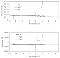
- FIG. 7 is a diagram illustrating a correlation between a bias voltage applied to the gas sensor of FIG. 1 and an impedance of carbon nanotube powder.
- FIG. 8 is a diagram for describing a chip including the gas sensor of FIG. 1.
- FIG. 9 is a view illustrating a result of performing heat treatment or washing on the chip of FIG. 8.
- FIG. 10 is a diagram illustrating a result of increasing sensitivity and recovery speed of a gas sensor when the chip of FIG. 8 is heat-treated at a high temperature.
- FIG. 1 is a view showing a gas sensor according to an embodiment of the present invention.
- the gas sensor 100 includes a substrate 110, an insulating layer 120, The first electrode 130 and the second electrode 140 are provided.
- the substrate 110 may be a flexible printed circuit board implemented with a film such as polyimide.
- the first electrode 130 and the second electrode 140 are formed on the substrate 110 and spaced apart from each other.
- An insulating layer 120 may be formed between the first electrode 130, the second electrode 140, and the substrate 110.
- the first electrode 130 and the second electrode 140 may be made of various materials such as Au, Ti, or an alloy thereof. Since the first electrode 130 and the second electrode 140 are formed on one substrate 110, the manufacturing process may be simplified.
- AC power AC may be applied to the first electrode 130 and the second electrode 140.
- the first electrode 130 and the second electrode 140 are each inter-digitated with each other. It may include a plurality of first sub-electrodes 132 and the second sub-electrodes 142 formed in a digitated form. That is, the plurality of first sub-electrodes 132 and the second sub-electrodes 142 face each other and are spaced apart from each other, such that the second sub-electrodes 142 are positioned between the first sub-electrodes 132.
- the first sub electrodes 132 are positioned between the second sub electrodes 142.
- the first sub-electrodes 132 may be formed in a comb-like shape integrally formed with the first electrode 130 and extending toward the second electrode 140.
- the second sub-electrodes 142 may be formed integrally with the second electrode 140 and may have a comb-shaped shape extending toward the first electrode 130.
- Carbon nanotube powder may be distributed between the first electrode 130 and the second electrode 140, that is, between the first sub-electrodes 132 and the second sub-electrodes 142.
- the present invention is not limited thereto, and nanowire powder may be used instead of carbon nanotube powder (CNT).
- the nanowire is a wire structure having a size in nanometers, and may be applied between the first electrode 130 and the second electrode 140 in the same manner as the carbon nanotube powder (CNT) described below.
- the impedance can be changed accordingly. Therefore, for convenience of description, hereinafter, only carbon nanotube powder (CNT) will be described. However, those of ordinary skill in the art to which the present invention pertains may easily perform the gas sensor of the present invention using the nanowire powder from the description of the following carbon nanotube powder (CNT).
- the carbon nanotube when used in a gas sensor, the carbon nanotube can be operated at room temperature, and the impedance change is large even when reacting with harmful gases such as NH 3 , NO 2, or volatile organic compounds (VOCs). Sensitivity is very good. In addition, there is an advantage that the reaction rate and response rate is fast.
- harmful gases such as NH 3 , NO 2, or volatile organic compounds (VOCs).
- Carbon nanotubes originally have hydrophobic properties because of the structure of carbon nanotubes.
- surface defects of carbon nanotubes have a strong bonding force and thus easily bond with other molecules. Therefore, hydrophobic or hydrophilic properties of the carbon nanotubes can be controlled by surface defects of the carbon nanotubes.
- the gas sensor using the carbon nanotubes can give a selectivity to a specific gas, it is possible to accurately measure the concentration of various gases.
- the gas sensor using the carbon nanotube according to the prior art has a problem that it takes a long time to initialize the sensor after the sensing operation is finished or the sensing sensitivity is lowered.
- the gas sensor 100 can reduce the recovery speed (time required for initialization) while increasing the sensitivity. This is described in more detail.
- the carbon nanotube powder CNT dispersed between the first electrode 130 and the second electrode 140 may be applied to the type of gas when AC power is applied.
- the impedance change amount of the carbon nanotube powder (CNT) dispersed between the first electrode 130 and the second electrode 140 is measured by a measuring device (not shown) such as an LCR (inductance, capacitance and resistance) meter. Since dispersed carbon nanotubes are in the form of very small tubes with diameters of several tens of nanometers, a strong electric field is applied to the ends. As a result, adsorption of gas molecules on the ends and surfaces of the carbon nanotubes causes large changes in capacitance. Will appear. Thus, by measuring the impedance to be changed, the concentration of the gas can be measured.
- the carbon nanotube powder (CNT) is DCE (1,2-dichloroethane, [ClCH 2 CH 2 Cl]), SDS (Sodium Dodecyl Sulfate, [CH 3 (CH 2) 11 OSO 3 Na +]) and NaDDBS (Sodium Dodecylbenzene Sulfonate, [CH 3 (CH 2) 11C6H4SO3Na +]), and the like, may be dispersed in a solvent and applied to the first electrode 130 and the second electrode 140.
- the carbon nanotube powder (CNT) may be evenly applied between the first electrode 130 and the second electrode 140. Therefore, the sensing sensitivity can be improved.
- the gas sensor 100 may apply carbon nanotube powder (CNT) dispersed in a solvent by a surfactant in a spray method.
- carbon nanotube powder (CNT) When carbon nanotube powder (CNT) is applied using a spray, it is as shown in (b) of FIG. 2 rather than dropping a solution in which the carbon nanotube powder is dissolved ((a) of FIG. 2).
- carbon nanotube powder (CNT) may be uniformly applied.
- the spray method has an advantage that the carbon nanotube formation conditions can be precisely adjusted than when the solution in which the carbon nanotube powder is dispersed is dropped.
- the gas sensor 100 shows the carbon nanotube powder (CNT) dispersed by a surfactant in FIG.
- the solution is formed in the shape of hemisphere by the surface tension of the solution in which the carbon nanotube powder is dispersed at the end of the tube by using a tube having an inner diameter similar to that of the electrode, and the solution is formed in the first electrode 130 It can be dispersed in a stamping (stamping) method in the space between the second electrode 140.
- Carbon nanotube powder (CNT) dispersed in a stamping method as shown in Figure 4 (a), can be applied quickly, simply and uniformly.
- the carbon nanotube powder (CNT) can solve the problem of dense to the edge of the drop of the solution have. That is, in the case of the stamping method, the carbon nanotube powder (CNT) is evenly distributed, so that the sensitivity of the gas sensor may be improved.
- the gas sensor 100 may improve the sensitivity of the dispersion of the solution in which the carbon nanotube powder (CNT) is dissolved by spraying or stamping.
- CNT carbon nanotube powder
- sensitivity may increase.
- FIG. 5 which shows an experimental example of the correlation between the interval between the first electrode 130 and the second electrode 140 and the sensitivity, it can be seen that the sensitivity is increased at about 5 micrometers or less.
- the specific gas may be improved in sensitivity at a specific frequency.
- Gas sensor according to an embodiment of the present invention by using a characteristic that the specific gas has a good sensitivity and recovery rate at a specific frequency, by checking the sensitivity to the gas at three or more different frequencies, respectively, selectivity to the gas Can have
- the sensitivity or the recovery speed for the specific gas can be set.
- the gas sensor 100 may further include a heater 150.
- the heater 150 may be located between the substrate 110 and the electrodes 130 and 140. A current is supplied to the heater 150 to maintain the temperature of the gas sensor 100, thereby improving the sensitivity and reliability of the sensor.
- the heater mainly uses platinum, which is stable at high temperatures, and may be implemented as a material having a moderate thermal expansion coefficient between the substrate and the heater material, such as titanium (Ti), to solve the problem of peeling off due to the difference in thermal expansion coefficient with the substrate. have.
- the gas sensor 100 according to the embodiment of the present invention may further include vias 160 connecting the first electrode 130 or the second electrode 140.
- the gas sensor 100 according to the exemplary embodiment of the present invention may set the gas to be sensed by applying the bias voltage DC to the via 160.
- the type of gas sensed varies according to the magnitude of the bias voltage DC. That is, the sensitivity of a particular gas at a specific bias voltage can be improved. For example, in a section in which the bias voltage is about ⁇ 2V to 0V, sensitivity to nitrogen dioxide may be improved.
- the gas sensor 100 may set the type of gas to be sensed by differently setting the bias voltage DC.
- FIG. 8A illustrates an operating power supply (AC, AC) for supplying a voltage to the gas sensor 100 of FIG. 1 and the first electrode 130 and the second electrode 140 of the gas sensor 100 of FIG. 1.
- the gas sensor 100 may be positioned in the middle of the voltage pads VPAD and the heater pads HPAD.
- A, b, c, and d of FIG. 1B may be connected to a ', b', c ', and d' of FIG. 8A, respectively.
- the heater is mainly composed of a platinum resistor that is stable at high temperature and generates heat when a current flows.
- the heater is heated to generate heat, and when the heater power is controlled, the temperature of the heater can be controlled.
- the sensor may have a selectivity to gas by applying a bias voltage between the heater pattern and the electrode using the same pad.
- the chip CIP of FIG. 8A or the wafer of FIG. 8B may be heated or cleaned.
- the surfactant is removed to increase the reaction and recovery rate of the gas sensor. Faster.
- the chip CIP of FIG. 8A or the wafer of FIG. 9B is washed with alcohol or water and then thermally treated, as shown in FIG. 9B, the surfactant is removed to form a gas. The response and recovery rate of the sensor is faster.
- the uniformity of the carbon nanotube powder (CNT) applied to the region between the first electrode 130 and the second electrode 140 can have a significant effect on the sensitivity of the sensor.
- the chip CIP of FIG. 8A or the wafer of FIG. 8B can also be heat treated using a halogen lamp or the like. By the heat treatment at a high temperature, the sensitivity and reaction speed of the gas sensor as shown in FIG. 10 (a) can be improved as shown in FIG. 10 (b).
- the gas sensor according to the present invention has an advantage of improving sensitivity and reaction speed.
- by varying the bias voltage to improve the sensitivity to a specific gas, or by varying the frequency of the AC power source can be variously designed according to the needs of the user, such as adjusting the sensitivity or recovery rate.
- the present invention can be used in the field of manufacturing gas sensors.
Landscapes
- Chemical & Material Sciences (AREA)
- Engineering & Computer Science (AREA)
- Nanotechnology (AREA)
- Health & Medical Sciences (AREA)
- Life Sciences & Earth Sciences (AREA)
- Biochemistry (AREA)
- General Physics & Mathematics (AREA)
- Electrochemistry (AREA)
- Chemical Kinetics & Catalysis (AREA)
- Analytical Chemistry (AREA)
- Materials Engineering (AREA)
- General Health & Medical Sciences (AREA)
- Physics & Mathematics (AREA)
- Immunology (AREA)
- Pathology (AREA)
- Crystallography & Structural Chemistry (AREA)
- Manufacturing & Machinery (AREA)
- Microelectronics & Electronic Packaging (AREA)
- Molecular Biology (AREA)
- Investigating Or Analyzing Materials By The Use Of Fluid Adsorption Or Reactions (AREA)
Abstract
La présente invention concerne un capteur de gaz. Un capteur de gaz cité à titre d'exemple dans l'invention comprend: une première électrode et une seconde électrode qui sont formées sur une plaque de base, placées à distance l'une de l'autre et sur lesquelles est appliquée une source de courant alternatif. Une poudre de nanotubes de carbone ou une poudre de nanocâbles est déposée dans les régions formées entre la première électrode et la seconde électrode et l'impédance de la poudre de nanotubes change en fonction de la concentration d'un gaz.
Applications Claiming Priority (2)
| Application Number | Priority Date | Filing Date | Title |
|---|---|---|---|
| KR10-2009-0065227 | 2009-07-17 | ||
| KR1020090065227A KR20110007676A (ko) | 2009-07-17 | 2009-07-17 | 가스 센서 |
Publications (3)
| Publication Number | Publication Date |
|---|---|
| WO2011008043A2 true WO2011008043A2 (fr) | 2011-01-20 |
| WO2011008043A9 WO2011008043A9 (fr) | 2011-03-31 |
| WO2011008043A3 WO2011008043A3 (fr) | 2011-05-12 |
Family
ID=43449987
Family Applications (1)
| Application Number | Title | Priority Date | Filing Date |
|---|---|---|---|
| PCT/KR2010/004635 Ceased WO2011008043A2 (fr) | 2009-07-17 | 2010-07-16 | Capteur de gaz |
Country Status (2)
| Country | Link |
|---|---|
| KR (1) | KR20110007676A (fr) |
| WO (1) | WO2011008043A2 (fr) |
Cited By (3)
| Publication number | Priority date | Publication date | Assignee | Title |
|---|---|---|---|---|
| US11346806B2 (en) | 2017-11-20 | 2022-05-31 | Honeywell International Inc. | Low profile ionization detector |
| US12306127B2 (en) | 2022-07-07 | 2025-05-20 | Ge Infrastructure Technology Llc | System and method for multi-gas sensing at a single operating temperature |
| US12669485B2 (en) | 2022-07-07 | 2026-06-30 | Ge Infrastructure Technology Llc | System and method for multi-gas sensing at several operating temperatures |
Families Citing this family (5)
| Publication number | Priority date | Publication date | Assignee | Title |
|---|---|---|---|---|
| KR101492389B1 (ko) * | 2013-10-18 | 2015-02-12 | 공주대학교 산학협력단 | 정전식 기체센서 |
| KR102651194B1 (ko) * | 2019-05-21 | 2024-03-27 | 울산과학기술원 | 공중 부유형 탄소 나노와이어를 이용한 3ω 방법 기반 가스센서 및 그 제조 방법 |
| KR102435557B1 (ko) * | 2020-04-10 | 2022-08-24 | 포항공과대학교 산학협력단 | 플렉시블 가스 센서 및 그 제조 방법 |
| KR102832844B1 (ko) * | 2020-08-21 | 2025-07-10 | 주식회사 엘지에너지솔루션 | 탄소나노튜브 분산액 평가 방법 |
| KR102608526B1 (ko) * | 2021-10-05 | 2023-12-04 | 한국과학기술원 | 고속 동작이 가능한 공중부유 나노와이어 구조체 |
Family Cites Families (4)
| Publication number | Priority date | Publication date | Assignee | Title |
|---|---|---|---|---|
| JP2002082082A (ja) * | 2000-09-07 | 2002-03-22 | Matsushita Refrig Co Ltd | 臭気センサー及びその製造方法 |
| KR100837397B1 (ko) * | 2006-01-05 | 2008-06-17 | 삼성전자주식회사 | 탄소나노튜브를 이용한 개스 센서 및 그 측정방법 |
| KR100809421B1 (ko) * | 2006-09-29 | 2008-03-05 | 한국전자통신연구원 | 나노 크기의 감지물질을 갖는 다중가스 감지센서 및 이를이용한 감지방법 |
| JP5140493B2 (ja) * | 2007-09-26 | 2013-02-06 | 独立行政法人国立高等専門学校機構 | ガスセンサー及びガスセンサー製造方法 |
-
2009
- 2009-07-17 KR KR1020090065227A patent/KR20110007676A/ko not_active Withdrawn
-
2010
- 2010-07-16 WO PCT/KR2010/004635 patent/WO2011008043A2/fr not_active Ceased
Cited By (3)
| Publication number | Priority date | Publication date | Assignee | Title |
|---|---|---|---|---|
| US11346806B2 (en) | 2017-11-20 | 2022-05-31 | Honeywell International Inc. | Low profile ionization detector |
| US12306127B2 (en) | 2022-07-07 | 2025-05-20 | Ge Infrastructure Technology Llc | System and method for multi-gas sensing at a single operating temperature |
| US12669485B2 (en) | 2022-07-07 | 2026-06-30 | Ge Infrastructure Technology Llc | System and method for multi-gas sensing at several operating temperatures |
Also Published As
| Publication number | Publication date |
|---|---|
| KR20110007676A (ko) | 2011-01-25 |
| WO2011008043A9 (fr) | 2011-03-31 |
| WO2011008043A3 (fr) | 2011-05-12 |
Similar Documents
| Publication | Publication Date | Title |
|---|---|---|
| WO2011008043A9 (fr) | Capteur de gaz | |
| Khan et al. | All printed full range humidity sensor based on Fe2O3 | |
| CN109100075A (zh) | 一种用于电子皮肤的柔性压力传感器及制备方法 | |
| US9964508B2 (en) | Sensing water vapour | |
| CN111157039B (zh) | 一种可同时检测湿度、温度和流量的多功能气体传感器及其制备方法 | |
| CN1379731A (zh) | 气敏元件及其制造方法 | |
| CN109211459A (zh) | 一种柔性碳纳米管热敏薄膜剪应力微传感器及其制造方法 | |
| CN115343346B (zh) | 离子传感器及其无掩模制备方法及体液传感监测系统 | |
| Yu et al. | Facile Preparation of Carbon Nanotube‐Based Skin‐Like Pressure Sensors | |
| JP6370111B2 (ja) | 容量型ガスセンサ及びその製造方法 | |
| WO2014034744A1 (fr) | Élément chauffant et dispositif de fixation, dispositif de formation d'image et dispositif de chauffe équipé ce dernier | |
| Padigi et al. | Carbon nanotube based aliphatic hydrocarbon sensor | |
| KR101431471B1 (ko) | 저 소비 전력형 가스 센서 | |
| CN117091732A (zh) | 一种具有湿度快速恢复特性的柔性复合传感器及制备方法 | |
| CN110514319A (zh) | 温度传感器及制造传感器单元与温度传感器的方法 | |
| Zhang et al. | A flexible calligraphy-integrated in situ humidity sensor | |
| KR100856577B1 (ko) | 탄소나노튜브 센서 및 그 제조방법 | |
| KR20150111246A (ko) | 바이오 센서 | |
| KR100809421B1 (ko) | 나노 크기의 감지물질을 갖는 다중가스 감지센서 및 이를이용한 감지방법 | |
| US7304490B2 (en) | In-situ wafer and probe desorption using closed loop heating | |
| WO2006073469A3 (fr) | Nanotubes a base de nanoparticules de silicium et leur procede de fabrication | |
| Maalaoui et al. | Towards miniaturized pH sensor based on carbon nanotubes assembled by DEP on titanium electrodes? | |
| CN107529233A (zh) | 一种基于铂电阻的加热和测温电路 | |
| Soukup et al. | Advanced screen printing for the fabrication of organic humidity sensors | |
| CN104391137A (zh) | 一种新型同步微区电化学成像和温度成像系统 |
Legal Events
| Date | Code | Title | Description |
|---|---|---|---|
| 121 | Ep: the epo has been informed by wipo that ep was designated in this application |
Ref document number: 10800054 Country of ref document: EP Kind code of ref document: A2 |
|
| NENP | Non-entry into the national phase |
Ref country code: DE |
|
| 122 | Ep: pct application non-entry in european phase |
Ref document number: 10800054 Country of ref document: EP Kind code of ref document: A2 |