WO2011052257A1 - 液晶表示素子 - Google Patents
液晶表示素子 Download PDFInfo
- Publication number
- WO2011052257A1 WO2011052257A1 PCT/JP2010/059128 JP2010059128W WO2011052257A1 WO 2011052257 A1 WO2011052257 A1 WO 2011052257A1 JP 2010059128 W JP2010059128 W JP 2010059128W WO 2011052257 A1 WO2011052257 A1 WO 2011052257A1
- Authority
- WO
- WIPO (PCT)
- Prior art keywords
- liquid crystal
- alignment film
- display element
- crystal display
- pair
- Prior art date
- Legal status (The legal status is an assumption and is not a legal conclusion. Google has not performed a legal analysis and makes no representation as to the accuracy of the status listed.)
- Ceased
Links
Images


Classifications
-
- G—PHYSICS
- G02—OPTICS
- G02F—OPTICAL DEVICES OR ARRANGEMENTS FOR THE CONTROL OF LIGHT BY MODIFICATION OF THE OPTICAL PROPERTIES OF THE MEDIA OF THE ELEMENTS INVOLVED THEREIN; NON-LINEAR OPTICS; FREQUENCY-CHANGING OF LIGHT; OPTICAL LOGIC ELEMENTS; OPTICAL ANALOGUE/DIGITAL CONVERTERS
- G02F1/00—Devices or arrangements for the control of the intensity, colour, phase, polarisation or direction of light arriving from an independent light source, e.g. switching, gating or modulating; Non-linear optics
- G02F1/01—Devices or arrangements for the control of the intensity, colour, phase, polarisation or direction of light arriving from an independent light source, e.g. switching, gating or modulating; Non-linear optics for the control of the intensity, phase, polarisation or colour
- G02F1/13—Devices or arrangements for the control of the intensity, colour, phase, polarisation or direction of light arriving from an independent light source, e.g. switching, gating or modulating; Non-linear optics for the control of the intensity, phase, polarisation or colour based on liquid crystals, e.g. single liquid crystal display cells
- G02F1/133—Constructional arrangements; Operation of liquid crystal cells; Circuit arrangements
- G02F1/1333—Constructional arrangements; Manufacturing methods
- G02F1/1337—Surface-induced orientation of the liquid crystal molecules, e.g. by alignment layers
- G02F1/133742—Surface-induced orientation of the liquid crystal molecules, e.g. by alignment layers for homeotropic alignment
-
- G—PHYSICS
- G02—OPTICS
- G02F—OPTICAL DEVICES OR ARRANGEMENTS FOR THE CONTROL OF LIGHT BY MODIFICATION OF THE OPTICAL PROPERTIES OF THE MEDIA OF THE ELEMENTS INVOLVED THEREIN; NON-LINEAR OPTICS; FREQUENCY-CHANGING OF LIGHT; OPTICAL LOGIC ELEMENTS; OPTICAL ANALOGUE/DIGITAL CONVERTERS
- G02F1/00—Devices or arrangements for the control of the intensity, colour, phase, polarisation or direction of light arriving from an independent light source, e.g. switching, gating or modulating; Non-linear optics
- G02F1/01—Devices or arrangements for the control of the intensity, colour, phase, polarisation or direction of light arriving from an independent light source, e.g. switching, gating or modulating; Non-linear optics for the control of the intensity, phase, polarisation or colour
- G02F1/13—Devices or arrangements for the control of the intensity, colour, phase, polarisation or direction of light arriving from an independent light source, e.g. switching, gating or modulating; Non-linear optics for the control of the intensity, phase, polarisation or colour based on liquid crystals, e.g. single liquid crystal display cells
- G02F1/133—Constructional arrangements; Operation of liquid crystal cells; Circuit arrangements
- G02F1/1333—Constructional arrangements; Manufacturing methods
- G02F1/1343—Electrodes
- G02F1/134309—Electrodes characterised by their geometrical arrangement
- G02F1/134363—Electrodes characterised by their geometrical arrangement for applying an electric field parallel to the substrate, i.e. in-plane switching [IPS]
Definitions
- the present invention relates to a liquid crystal display element. More specifically, the present invention relates to a liquid crystal display element suitable for a display method in which light is transmitted through a liquid crystal layer by applying a voltage to bend the liquid crystal molecules in the liquid crystal layer in a lateral direction.
- a liquid crystal display element (hereinafter abbreviated as LCD) is a display device characterized by thinness, light weight, and low power consumption. It is a mobile phone, PDA, car navigation system, personal computer monitor, TV, and information on the station premises. It has been adopted for many uses such as information displays such as boards and outdoor bulletin boards.
- Electric field type liquid crystal display elements include a TN (Twisted Nematic) mode, an OCB (Optically Compensated Bend) mode, and the like, which can satisfy characteristics such as high transmittance and high-speed response, respectively.
- a vertical electric field type liquid crystal display element in which the liquid crystal alignment when no voltage is applied is perpendicular to the substrate, there is a multi-domain vertical alignment (MVA) mode, and the liquid crystal alignment when no voltage is applied is perpendicular to the substrate.
- MVA multi-domain vertical alignment
- TBA Transverse Bend Alignment
- IPS In-plane Switching
- a liquid crystal device in which a liquid crystal having negative dielectric anisotropy is sandwiched between a pair of substrates, and at least one of the pair of substrates includes a pixel electrode and a pixel electrode on the pixel electrode.
- the alignment film provided on at least one of the pair of substrates is composed of an inorganic film having a porous structure, and a plurality of protrusions formed on the surface of the inorganic film on the liquid crystal layer side
- a liquid crystal device (see, for example, Patent Document 2) in which the convex portion has a major axis and a minor axis in a plan view is disclosed.
- an active matrix type liquid crystal display device in which an extrapolation length representing the strength of torsional coupling between the liquid crystal molecules and the alignment film surface at the interface between the alignment film and the liquid crystal layer is 10% or more of a pair of substrate gaps ( For example, see Patent Document 3.).
- a TBA mode liquid crystal display device or the like (see, for example, Patent Documents 4 to 10) is disclosed.
- JP 2008-225032 A JP 2008-191264 A JP 2005-189889 A JP-A-57-618 JP-A-10-186351 JP-A-10-333171 Japanese Patent Laid-Open No. 11-24068 JP 2000-275682 A JP 2002-55357 A JP 2001-159759 A
- the present invention has been made in view of the above-described present situation, and an object thereof is to provide a liquid crystal display element capable of sufficiently improving reliability and optical characteristics and capable of being driven at a low voltage. It is.
- the present invention is not limited to the TBA mode.
- the present inventors have made various studies on reducing the driving voltage in a liquid crystal display element capable of obtaining a high contrast.
- the initial alignment is vertical alignment, and the liquid crystal is directed toward the center of the non-electrode portion when an electric field is applied.
- the dielectric anisotropy ⁇ (hereinafter also simply referred to as ⁇ ) of the liquid crystal is about 20 (MVA). It cannot be driven without using a material of about -3 for the mode and about 5 for the TN mode. In general, as ⁇ is increased, the reliability as a material may decrease or the optical characteristics may decrease.
- the reason why the drive voltage becomes high in this way is as follows.
- the transmittance is determined by the liquid crystal of the non-electrode portion, the non-electrode portion is made as large as possible. Therefore, the space between the electrode portions is widened.
- the distance between the electrodes (that is, the cell thickness) is usually 3 to 4 ⁇ m in the MVA mode or the TN mode, but is about 8 ⁇ m in the TBA mode, for example, and the threshold voltage becomes high.
- the TBA mode since liquid crystal molecules are driven between a pair of comb-shaped electrodes formed on one substrate, the electric field becomes weaker as the substrate on the side opposite to the comb-shaped substrate is approached. (Insensitive area is present). This increases the threshold voltage.
- the inventors of the present invention have made it possible to increase the dielectric constant of the alignment film so that the electric field applied to the liquid crystal is sufficiently large, and to form a pole at the interface with the liquid crystal layer of the substrate.
- reducing the angular binding force is effective in reducing the ⁇ of the liquid crystal sufficiently, improving the reliability and optical characteristics, and reducing the driving voltage. .
- the present inventors have conducted various studies on specific methods for sufficiently improving the reliability and optical characteristics and reducing the driving voltage in the TBA mode and the like, and as a result, the vertical alignment film included in the substrate is inorganic.
- the electric field applied to the liquid crystal is sufficiently large, ⁇ of the liquid crystal is sufficiently small, and anchoring in the polar angle direction of the substrate at the interface with the liquid crystal layer is performed.
- the inventors have arrived at the present invention by conceiving that energy can be effectively reduced and the above-mentioned problems can be solved brilliantly.
- the present invention is a liquid crystal display element including a pair of substrates and a liquid crystal layer sealed between the pair of substrates, wherein the liquid crystal layer contains liquid crystal molecules having positive dielectric anisotropy. And at least one of the pair of substrates has a pair of comb-shaped electrodes, and at least one of the pair of substrates has a vertical alignment film in a display region on a surface in contact with the liquid crystal layer, and the vertical
- the alignment film is a liquid crystal display element that is an inorganic alignment film formed of an inorganic material.
- the liquid crystal display element of the present invention is a liquid crystal display element including a pair of substrates and a liquid crystal layer sealed between the pair of substrates.
- the liquid crystal layer is filled with liquid crystal molecules whose orientation is controlled by application of a constant voltage.
- a voltage can be applied to the liquid crystal layer and the alignment of liquid crystal molecules can be controlled.
- liquid crystal molecules having a positive dielectric anisotropy are used as the liquid crystal molecules.
- the liquid crystal molecules are aligned along the direction of the electric field by applying a voltage to the liquid crystal layer, and the liquid crystal molecules have an arch shape, for example. You can get a corner.
- the dielectric constant anisotropy ⁇ of the liquid crystal molecules is preferably 10 or more. Thereby, the effect of the present invention can be exhibited more remarkably. More preferably, it is 15 or more.
- the upper limit is preferably 25 or less.
- the pair of substrates has a pair of comb electrodes.
- the pair of comb-shaped electrodes is, for example, a common voltage in which one comb-shaped electrode is provided in pixel units and a signal voltage is applied, and the other comb-shaped electrode is maintained at a constant voltage.
- an electric field for example, a horizontal electric field
- the distance between the pair of comb electrodes is preferably 7 to 9 ⁇ m, for example.
- At least one of the pair of substrates has a vertical alignment film on a surface in contact with the liquid crystal layer, and the vertical alignment film is an inorganic alignment film formed of an inorganic material.
- the inorganic alignment film preferably aligns the liquid crystal molecules substantially perpendicularly to at least one of the pair of substrates when no voltage is applied.
- the inorganic alignment film has an inclination of the liquid crystal molecules close to the surface when no voltage is applied, approximately 90 ° (90 ° ⁇ 0-4) in the polar angle direction when the direction parallel to the substrate surface is 0 °.
- An inorganic alignment film defined by The orientation may be due to the material of the inorganic orientation film or may be due to the structure of the inorganic orientation film.
- the inorganic alignment film is preferably provided over the entire display region when viewed from the normal direction of the substrate surface.
- the configuration of the liquid crystal display element of the present invention is not particularly limited by other components as long as such components are essential.
- the preferable form in the liquid crystal display element of this invention is demonstrated in detail below.
- the said inorganic material has the form whose dielectric constant is 4-6.
- the electric field applied to the liquid crystal can be made sufficiently large.
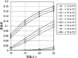
- a liquid crystal having a small dielectric anisotropy ⁇ can be used to sufficiently improve the reliability and optical characteristics as a material, or a desired transmittance can be achieved even when the threshold voltage is low ( 7 and FIG. 8 partially enlarged from FIG. 7).
- a silicon-based inorganic material usually has a dielectric constant of 6 or less, and the form in which the inorganic material contains silicon is also a preferred form of the present invention. 7 and 8, the transmittance ratio when the transmittance 100% is 1 is shown as “transmittance”.
- the inorganic alignment film is preferably made of a material having a SiO bond. By using a material having a SiO bond, the anchoring energy for the liquid crystal molecules can be lowered.
- the said inorganic alignment film has the form provided only in the board
- the said inorganic alignment film has a form formed by the printing method, the spin coating method, or the inkjet method.
- the liquid crystal display element of the present invention the liquid crystal display element can thereby be easily manufactured, and the throughput can be sufficiently improved.
- the printing method, spin coating method, or ink jet method an inorganic alignment film that vertically aligns liquid crystal molecules when no voltage is applied can be obtained.
- the present invention it is possible to sufficiently improve the reliability and optical characteristics as a material by adopting a liquid crystal having a small dielectric anisotropy ⁇ in a liquid crystal display element having an initial alignment of vertical alignment. It is possible to perform low voltage driving.
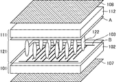
- FIG. 1 It is a perspective schematic diagram of the liquid crystal display element of Embodiment 1 which concerns on this invention. It is a cross-sectional schematic diagram of the liquid crystal display element of Embodiment 1 which concerns on this invention.
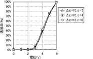
- 6 is a graph showing voltage-transmittance characteristics of TBA mode cells of Examples 1 and 2 and Comparative Example 1 when the dielectric anisotropy ⁇ of the liquid crystal is 10.
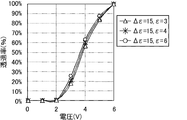
- 6 is a graph showing voltage-transmittance characteristics of TBA mode cells of Examples 1 and 2 and Comparative Example 1 when the dielectric anisotropy ⁇ of liquid crystal is 15.
- 6 is a graph showing voltage-transmittance characteristics of TBA mode cells of Examples 1 and 2 and Comparative Example 1 when the dielectric anisotropy ⁇ of the liquid crystal is 20.
- 6 is a graph showing voltage-transmittance characteristics of the TBA mode cells of Examples 1 and 2 and Comparative Example 1 when the dielectric anisotropy ⁇ of the liquid crystal is 25. 6 is a graph showing dielectric anisotropy-transmittance characteristics of each liquid crystal used in a TBA mode cell. It is the graph which expanded the graph of FIG. 7 partially. 6 is a schematic cross-sectional view illustrating a configuration of a liquid crystal display element of Embodiment 2. FIG.
- FIG. 1 is a schematic perspective view of a liquid crystal display element according to Embodiment 1 of the present invention.
- FIG. 2 is a schematic cross-sectional view of the liquid crystal display element of Embodiment 1 according to the present invention.
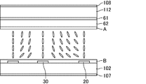
- the liquid crystal display element according to the first embodiment of the present invention is sandwiched between the array substrate 101, the counter substrate 111 facing the glass substrate 102, and the array substrate 101 and the counter substrate 111.
- the liquid crystal layer 121 is formed.
- the array substrate 101 has a pair of comb-shaped electrodes 103 that generate a lateral electric field, and is mainly a glass substrate 102 on which an alignment film B including a vertical alignment group is stacked.
- the counter substrate 111 mainly includes a glass substrate 112 on which a color filter (CF) 113 and an alignment film A including a vertical alignment group are stacked.
- CF color filter
- Each of the pair of comb-shaped electrodes 103 is a pixel electrode and a common electrode, and includes comb teeth as a basic configuration.
- the comb teeth of the picture element electrode and the comb teeth of the common electrode are parallel to each other and are alternately meshed with each other with a space therebetween.
- the picture element electrode is an electrode arranged for each picture element unit constituting the display area, and is supplied with an image signal.
- the common electrode is an electrode that is electrically conductive regardless of the boundary of the picture element, and is supplied with a common signal.
- nematic liquid crystal molecules nematic liquid crystal having positive dielectric anisotropy
- the positive nematic liquid crystal molecules (nematic liquid crystal having positive dielectric anisotropy) 122 are bend-oriented in the lateral direction along the applied electric field. In the electrode forming portion and the central portion between the electrodes, the vertical alignment is maintained, and the liquid crystal molecules located in the non-electrode portion contribute to the transmission.
- the liquid crystal display element according to the first embodiment of the present invention includes a liquid crystal layer 121 including positive nematic liquid crystal (nematic liquid crystal having positive dielectric anisotropy) aligned perpendicular to the substrate surface in the absence of voltage.
- a liquid crystal layer 121 including positive nematic liquid crystal (nematic liquid crystal having positive dielectric anisotropy) aligned perpendicular to the substrate surface in the absence of voltage is a TBA mode liquid crystal display element in which an electric field in the horizontal direction (substrate surface direction) is applied to transfer liquid crystal molecules in the liquid crystal layer to a bend alignment in the horizontal direction.
- the liquid crystal display element of this embodiment includes a resin bead spacer that defines the liquid crystal layer thickness (cell gap) between the array substrate 101 and the counter substrate 111, and a seal for sealing the liquid crystal layer 121. It has a member.
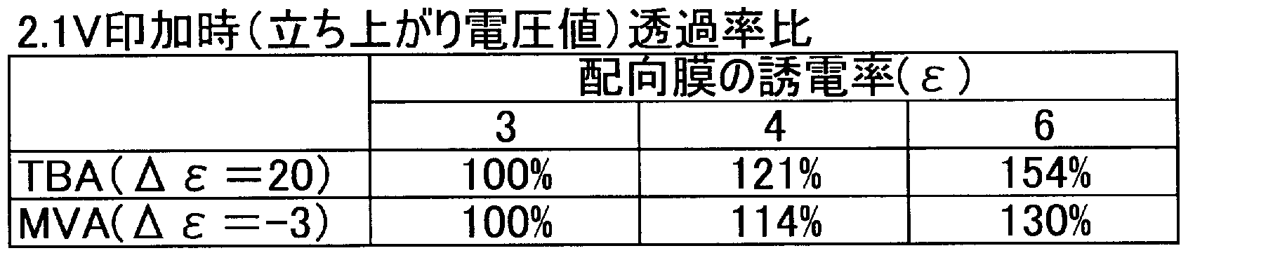
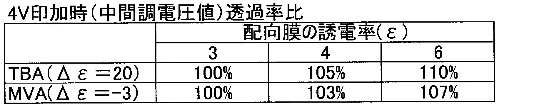
- Example 1 (Examples 1 and 2 and Comparative Example 1) As shown in Table 1 below, the dielectric constant of organic substances is generally about 3 or less, and the dielectric constant of inorganic substances is about 4 or more. Note that ⁇ ⁇ represents a relative dielectric constant.
- the dielectric constant ⁇ of the alignment film A and alignment film B is 3 corresponding to an organic material and 4 and 6 corresponding to an inorganic material (respectively comparative examples) 1 and Examples 1 and 2) show the voltage versus transmittance (alignment film thickness 1000 mm) in the TBA mode in FIGS. 3 to 6, respectively.
- FIG. 3 is a graph showing voltage-transmittance characteristics of the TBA mode cells of Examples 1 and 2 and Comparative Example 1 when the dielectric anisotropy ⁇ of the liquid crystal is 10.
- FIG. 4 is a graph showing voltage-transmittance characteristics of the TBA mode cells of Examples 1 and 2 and Comparative Example 1 when the dielectric anisotropy ⁇ of the liquid crystal is 15.
- FIG. 5 is a graph showing voltage-transmittance characteristics of the TBA mode cells of Examples 1 and 2 and Comparative Example 1 when the dielectric anisotropy ⁇ of the liquid crystal is 20.
- FIGS. 3 to 6 are graph showing voltage-transmittance characteristics of the TBA mode cells of Examples 1 and 2 and Comparative Example 1 when the dielectric anisotropy ⁇ of the liquid crystal is 25.
- ⁇ shown in FIGS. 3 to 6 indicates the dielectric anisotropy of the liquid crystal.
- ⁇ represents the dielectric constant of the vertical alignment film. 3 to 6, it can be seen that the alignment film having a high dielectric constant ⁇ achieves a high transmittance at a low voltage.
- the following can be said. (1) If the liquid crystal has the same ⁇ , the larger the ⁇ of the alignment film, the higher the rise or the low transmittance can be achieved. Therefore, the liquid crystal display element can be driven with a low voltage.
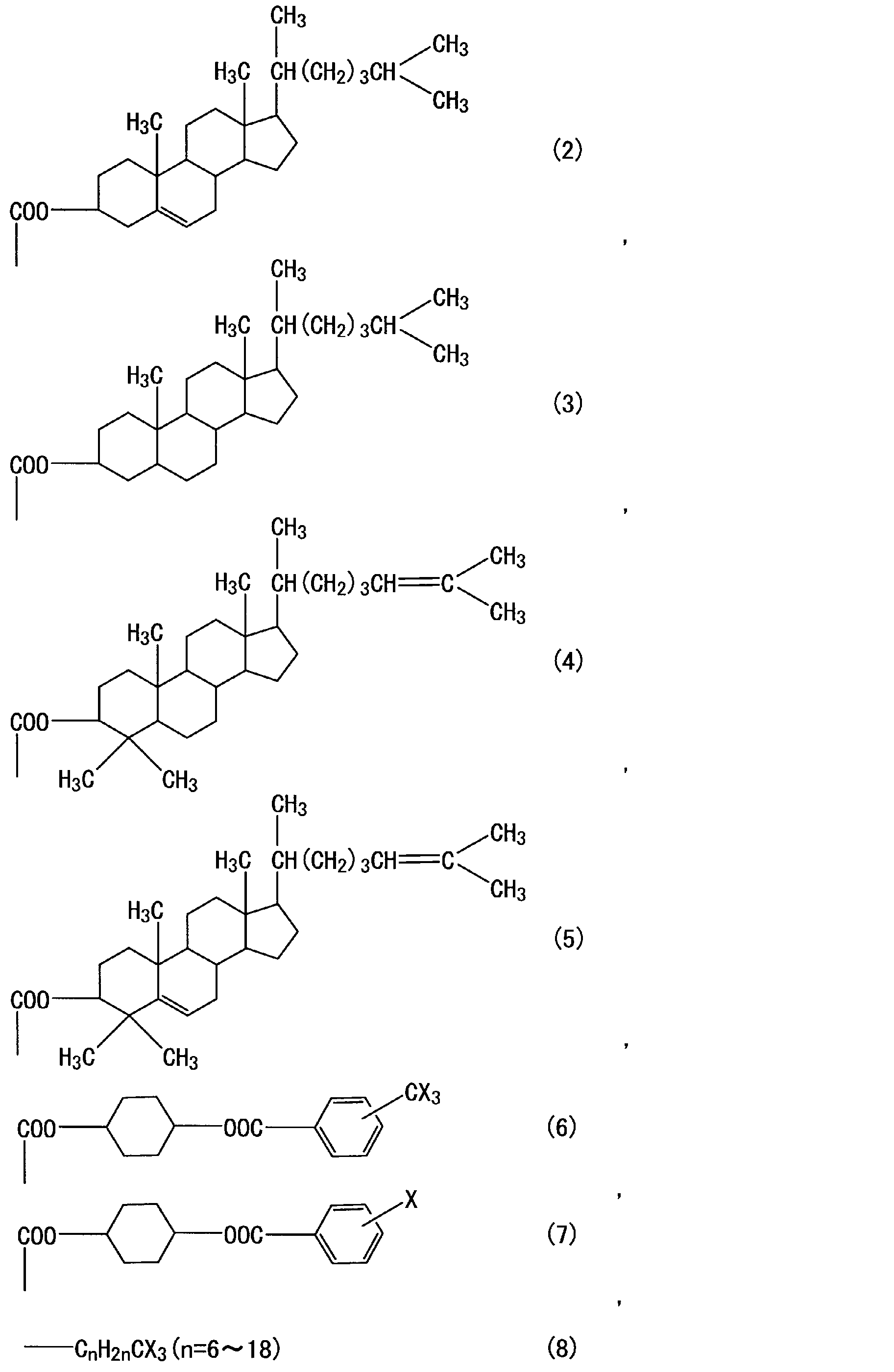
- an inorganic alignment film including a chemical structure represented by the following chemical formula (1) it is preferable to use an inorganic alignment film including a chemical structure represented by the following chemical formula (1).
- the following chemical formula (1) has a vertical alignment group -Y at the end of the side chain of the organosiloxane skeleton that is the main chain.
- the following chemical formula (1) indicates that it is obtained by polycondensation of an alkoxysilane monomer.
- l and m represent the number of repeating structures in parentheses and are positive integers.
- Y for example, a long chain alkyl group, a long chain fluorine-containing alkyl group, a siloxane chain and the like are preferable. Of these, those represented by any one of the following chemical formulas (2) to (8) are particularly preferred.
- liquid crystal alignment material examples include a liquid crystal alignment treatment agent described in JP-A-9-230354, a liquid crystal alignment treatment agent described in International Publication No. 2003/042752, and an international publication No. 2005/052028. It is possible to use the liquid crystal aligning agent for vertical alignment described in the above, the liquid crystal aligning agent for vertical alignment described in WO 2006/070819, the vertical liquid crystal aligning agent described in JP-A-2006-30961, and the like. .
- Example 3 the liquid crystal display element of Example 3 was produced as follows.
- a glass substrate on the side of the array substrate which is provided with a pair of transparent electrodes made of ITO (Indium Tin Oxide) or the like on the surface, is prepared on the glass substrate and the pair of comb electrodes.
- a vertical alignment film inorganic solution having the chemical structure represented by the chemical formula (1) is applied by spin coating under the condition of 1000 mm after firing, and then the substrate after application of the solution at 200 ° C.
- the inorganic alignment film was formed by baking for about 1 hour.
- variety of the comb tooth which a pair of comb-shaped electrode has was 4.0 micrometers, and the space
- interval of comb teeth was 8.0 micrometers (line / space 4.0 micrometers / 8.0 micrometers).
- an inorganic alignment film was formed on the glass substrate on the counter substrate side by the same process. Thereafter, resin bead spacers having a diameter of a desired cell thickness (d) are arranged on the array substrate by spraying or the like, and on the other hand, an epoxy-based seal resin is printed on the counter substrate, and these are bonded to each other at 180 ° C. Then, the sealing resin was cured for 2 hours to prepare a liquid crystal cell.
- positive type nematic liquid crystal (nematic liquid crystal having positive dielectric anisotropy) is sealed in a liquid crystal cell by vacuum injection, and then a polarizing plate is placed on the surface of each glass substrate opposite to the liquid crystal layer.
- the liquid crystal display element (Example 3) was produced by bonding. Encapsulated between the pair of substrates.
- ⁇ n is a value at which d ⁇ n is approximately ⁇ / 2 when voltage is applied, and ⁇ is 22.
- the vertical alignment film A is formed using an organic alignment film SE-1211 (manufactured by Nissan Chemical Industries, Ltd.) having no SiO bond instead of the above-described inorganic solution for the vertical alignment film as a material of the vertical alignment film.
- the vertical alignment film B is formed (Example 5), and the vertical alignment film A and the vertical alignment film B are formed (Comparative Example 1). Then, a liquid crystal display element was produced and the voltage-transmittance characteristics were measured in the same manner.
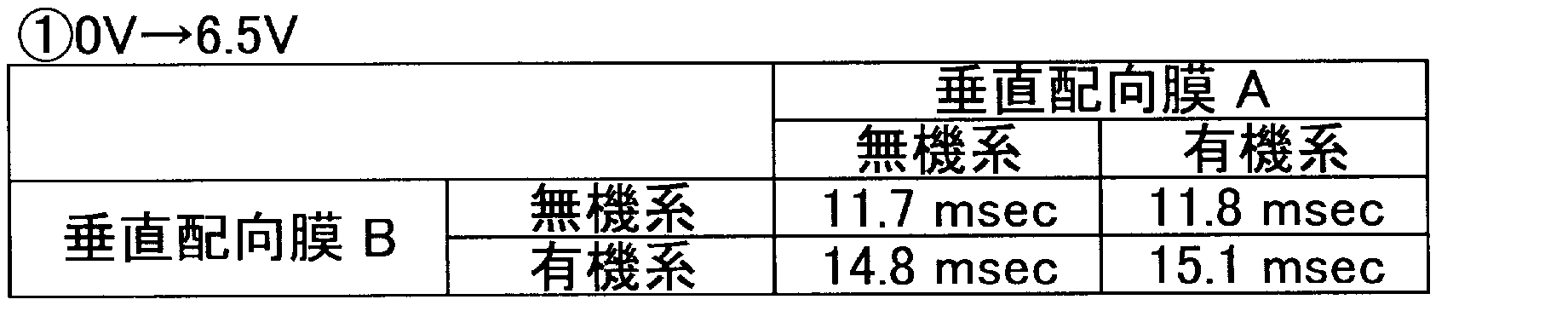
- (1) Table 4 below shows the results when a voltage of 0 V to 6.5 V was applied.
- Table 5 shows the results when a voltage of 6.5 V ⁇ 0 V was applied.
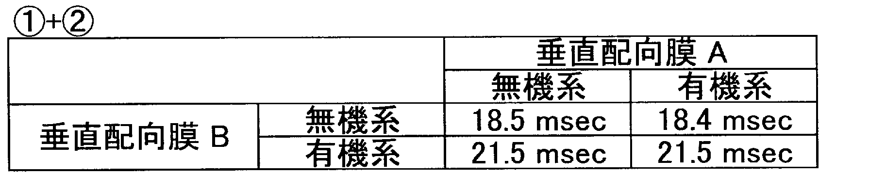
- it shows in Table 6 about the sum total of (1) and (2).
- the inorganic alignment film is provided on a substrate having a pair of comb-shaped electrodes, in particular, only on a substrate having a pair of comb-shaped electrodes. It was found that the ring energy can be reduced, and as a result, the effect of reducing the threshold voltage can be obtained.
- the inorganic alignment film including the SiO bond and the vertical alignment group Y is exemplified as the inorganic alignment film, but the present invention is not limited to this, and other inorganic alignment films such as AlOx, SiOx, TiOx, SiC, and the like are used. Is also possible.
- the inorganic alignment film may be a laminated film of these inorganic dielectrics, and can be combined as appropriate.
- Al aluminum
- Ga gallium
- In indium
- Si silicon
- Ge germanium
- Sn tin
- Ti titanium
- Zr zirconium
- Hf hafnium
- the liquid crystal display element of the present embodiment is further equipped with a drive circuit, a backlight (illumination device), etc., so that information such as mobile phones, PDAs, car navigation systems, personal computer monitors, televisions, information boards in stations, outdoor bulletin boards, etc. It can be used as a display or the like.
- the liquid crystal display element of this embodiment is different from that of Embodiment 1 in the following points. That is, the liquid crystal display element of this embodiment has a counter electrode on the counter substrate side. Specifically, as shown in FIG. 9, the counter electrode 61, the dielectric layer (insulating layer) 62, and the vertical alignment film A are laminated in this order on the main surface of the glass substrate 112 on the liquid crystal layer 121 side. Yes. Note that a color filter 113, a black matrix (BM), or the like may be provided between the counter electrode 61 and the glass substrate 112.
- BM black matrix
- the counter electrode 61 is formed from a transparent conductive film such as ITO or IZO. Each of the counter electrode 61 and the dielectric layer 62 is formed without a break so as to cover at least the entire display region. A predetermined potential common to each picture element is applied to the counter electrode 61.
- the dielectric layer 62 is formed from a transparent insulating material. Specifically, it is formed from an inorganic insulating film such as silicon nitride, an organic insulating film such as acrylic resin, or the like.
- the glass substrate 102 is provided with a comb-shaped electrode including the pixel electrode 20 and the common electrode 30 and a vertical alignment film B, as in the first embodiment. Further, polarizing plates 107 and 108 are disposed on the outer main surfaces of the two substrates 102 and 112.
- the common electrode 30 and the counter electrode 61 may be grounded, the voltage having the same magnitude and polarity may be applied to the common electrode 30 and the counter electrode 61, or voltages having different magnitudes and polarities may be applied to each other. It may be applied.
- the liquid crystal display element according to the second embodiment can sufficiently improve reliability and optical characteristics as in the first embodiment, and can be driven at a low voltage. Further, the response speed can be improved by forming the counter electrode 61.
- the vertical alignment film A since the denseness of the inorganic alignment film is very high, by using the inorganic alignment film as the vertical alignment film A, impurities are eluted from the color filter 113 and the dielectric layer 62 to the liquid crystal layer 121. It becomes possible to prevent. That is, the vertical alignment film A can function as a barrier layer.
Landscapes
- Physics & Mathematics (AREA)
- Nonlinear Science (AREA)
- Spectroscopy & Molecular Physics (AREA)
- Mathematical Physics (AREA)
- Chemical & Material Sciences (AREA)
- Crystallography & Structural Chemistry (AREA)
- General Physics & Mathematics (AREA)
- Optics & Photonics (AREA)
- Liquid Crystal (AREA)
Abstract
Description
更に、上述した負の誘電率異方性を有する液晶と無機配向膜とを組み合わせた液晶装置においては、スループット(生産率)をより充分なものとし、液晶分子の傾斜方向の制御をより容易にすることが望まれるところであった。
本発明者らは、高コントラストを得ることができる液晶表示素子において、駆動電圧を低減させることについて種々検討したところ、初期配向は垂直配向であり、電界印加時に非電極部の中央に向かって液晶分子が倒れ込む表示方式であるTBAモードでの液晶分子の電圧印加時の動きに着目した。
所望の透過率をなるべく小さいΔεを持つ液晶を使って得るためには、高い電圧をかけなければならない。その傾向は、液晶のΔεがある程度大きい範囲(立ち上がり電圧である2V付近では、Δεが10以上程度)で顕著になる。
以下、本発明の液晶表示素子について詳述する。
上記液晶分子の誘電率異方性Δεは、10以上であることが好ましい。これにより、本発明の効果を更に顕著に発揮することが可能となる。より好ましくは、15以上である。上限値としては、25以下であることが好ましい。
なお、上記一対の櫛型電極の電極間距離は、例えば、7~9μmであることが好ましい。
また上記無機配向膜は、基板面法線方向からみたときに、表示領域全面に設けられていることが好ましい。
本発明の液晶表示素子における好ましい形態について以下に詳しく説明する。
図1は、本発明に係る実施形態1の液晶表示素子の斜視模式図である。
図2は、本発明に係る実施形態1の液晶表示素子の断面模式図である。
図1、図2に示すように、本発明に係る実施形態1の液晶表示素子は、アレイ基板101、ガラス基板102に対向する対向基板111、及び、アレイ基板101と対向基板111とに狭持される液晶層121で構成される。アレイ基板101は、横電界を発生する一対の櫛型電極103を有し、垂直配向基を含む配向膜Bを積層したガラス基板102を主体とする。対向基板111は、カラーフィルタ(CF)113及び垂直配向基を含む配向膜Aを積層したガラス基板112を主体とする。
下記表1に示されるように、一般的に有機物の誘電率はほぼ3以下であり、無機物の誘電率はほぼ4以上である。なお、εγは、比誘電率を表す。

図4は、液晶の誘電率異方性Δεを15にしたときの、実施例1、2及び比較例1のTBAモードのセルの電圧-透過率特性を表したグラフである。
図5は、液晶の誘電率異方性Δεを20にしたときの、実施例1、2及び比較例1のTBAモードのセルの電圧-透過率特性を表したグラフである。
図6は、液晶の誘電率異方性Δεを25にしたときの、実施例1、2及び比較例1のTBAモードのセルの電圧-透過率特性を表したグラフである。
なお、図3~6に示したΔεは、液晶の誘電率異方性を示す。また、εは、垂直配向膜の誘電率を示す。
図3~6より、誘電率εの高い配向膜の方が低電圧で高透過率を達成していることが分かる。
まとめると、以下のことがいえる。
(1)同じΔεの液晶であれば配向膜のεが大きいほうが低電圧での立ち上がり、又は、高透過率を達成することができる。したがって、液晶表示素子を低電圧で駆動させることが可能である。(2)ある電圧値である透過率を達成したい場合、配向膜のεが大きいほうが低いΔε値で到達することができる。したがって、よりΔεが低い液晶を採用することができ、その結果、液晶表示素子における信頼性向上、光学特性向上が可能である。
実施例3~5における無機配向膜14は、SiO結合(SiOx(x=1~3))及び垂直配向基Yを有する配向膜である。例えば、下記化学式(1)で示される化学構造を含む無機配向膜を用いることが好ましい。下記化学式(1)は、主鎖であるオルガノシロキサン骨格の側鎖末端に垂直配向基-Yを有する。なお、下記化学式(1)は、アルコキシシランモノマーを重縮合して得られるものであることを示している。

Yは、例えば、長鎖アルキル基、長鎖含フッ素アルキル基、シロキサン鎖等が好適なものとして挙げられる。中でも、下記化学式(2)~(8)のいずれか一つで示されるものであることが特に好ましい。
なお、液晶配向材料としては、例えば、特開平9-230354号公報に記載の液晶配向処理剤、国際公開第2003/042752号パンフレットに記載の液晶配向処理剤、国際公開第2005/052028号パンフレットに記載の垂直配向用液晶配向処理剤、国際公開第2006/070819号パンフレットに記載の垂直配向用液晶配向剤、特開2006-30961号公報に記載の垂直液晶配向剤等を用いることが可能である。

(2)6.5V→0Vの電圧印加時は、一般的には弱アンカリングの場合は応答が遅くなるが、本モードにおいては、ベンド状配向が内部応力により垂直配向に戻るので、弱アンカリングの影響による応答の遅れはほとんどない(表5)。
(1)と(2)との合計の応答で見ても、櫛歯電極側(垂直配向膜B)に無機配向膜を用いた場合の方が応答が速いことが分かる(表6)。
本実施形態の液晶表示素子は、以下の点で実施形態1と異なる。
すなわち、本実施形態の液晶表示素子は、対向基板側に対向電極を有する。具体的には、図9に示すように、ガラス基板112の液晶層121側の主面上には、対向電極61、誘電体層(絶縁層)62及び垂直配向膜Aがこの順に積層されている。なお、対向電極61とガラス基板112の間には、カラーフィルタ113や、ブラックマトリクス(BM)等が設けられてもよい。
30:共通電極
61:対向電極
62:誘電体層
101:アレイ基板
102,112:ガラス基板
103:櫛型電極
107,108:偏光板
111:対向基板
113:カラーフィルタ
121:液晶層
122:印加電界に沿ってベンド状配向する液晶分子
123:電界の印加方位
A,B:垂直配向膜
Claims (4)
- 一対の基板と、該一対の基板間に封止された液晶層とを含む液晶表示素子であって、
該液晶層は、正の誘電率異方性を有する液晶分子を含有し、
該一対の基板の少なくとも一方は、一対の櫛型電極を有し、
該一対の基板の少なくとも一方は、液晶層と接する側の面の表示領域に垂直配向膜を有し、
該垂直配向膜は、無機材料で形成された無機配向膜である
ことを特徴とする液晶表示素子。 - 前記無機材料は、誘電率が4以上、6以下であることを特徴とする請求項1に記載の液晶表示素子。
- 前記無機配向膜は、前記一対の櫛型電極を有する基板のみに設けられていることを特徴とする請求項1又は2に記載の液晶表示素子。
- 前記無機配向膜は、印刷法、スピンコーティング法又はインクジェット法で形成されたものであることを特徴とする請求項1~3のいずれかに記載の液晶表示素子。
Priority Applications (6)
| Application Number | Priority Date | Filing Date | Title |
|---|---|---|---|
| EP10826392.2A EP2495610A4 (en) | 2009-10-30 | 2010-05-28 | LIQUID CRYSTAL DISPLAY ELEMENT |
| BR112012010185A BR112012010185A2 (pt) | 2009-10-30 | 2010-05-28 | elemento de exibição de cristal líquido |
| JP2011538276A JPWO2011052257A1 (ja) | 2009-10-30 | 2010-05-28 | 液晶表示素子 |
| RU2012122206/28A RU2012122206A (ru) | 2009-10-30 | 2010-05-28 | Жидкокристаллический элемент отображения |
| US13/393,261 US20120176575A1 (en) | 2009-10-30 | 2010-05-28 | Liquid crystal display element |
| CN2010800347981A CN102472926A (zh) | 2009-10-30 | 2010-05-28 | 液晶显示元件 |
Applications Claiming Priority (4)
| Application Number | Priority Date | Filing Date | Title |
|---|---|---|---|
| JP2009250395 | 2009-10-30 | ||
| JP2009-250395 | 2009-10-30 | ||
| JP2010006692 | 2010-01-15 | ||
| JP2010-006692 | 2010-01-15 |
Publications (1)
| Publication Number | Publication Date |
|---|---|
| WO2011052257A1 true WO2011052257A1 (ja) | 2011-05-05 |
Family
ID=43921688
Family Applications (1)
| Application Number | Title | Priority Date | Filing Date |
|---|---|---|---|
| PCT/JP2010/059128 Ceased WO2011052257A1 (ja) | 2009-10-30 | 2010-05-28 | 液晶表示素子 |
Country Status (7)
| Country | Link |
|---|---|
| US (1) | US20120176575A1 (ja) |
| EP (1) | EP2495610A4 (ja) |
| JP (1) | JPWO2011052257A1 (ja) |
| CN (1) | CN102472926A (ja) |
| BR (1) | BR112012010185A2 (ja) |
| RU (1) | RU2012122206A (ja) |
| WO (1) | WO2011052257A1 (ja) |
Cited By (1)
| Publication number | Priority date | Publication date | Assignee | Title |
|---|---|---|---|---|
| RU2491316C1 (ru) * | 2011-12-30 | 2013-08-27 | Государственное образовательное учреждение высшего профессионального образования Московский государственный областной университет | Способ изготовления жидкокристаллической ячейки |
Families Citing this family (4)
| Publication number | Priority date | Publication date | Assignee | Title |
|---|---|---|---|---|
| KR20140046818A (ko) * | 2012-10-11 | 2014-04-21 | 삼성디스플레이 주식회사 | 표시 패널 및 이를 포함하는 표시 장치 |
| JP2014153605A (ja) * | 2013-02-12 | 2014-08-25 | Japan Display Inc | 液晶表示装置 |
| US10317733B2 (en) * | 2016-10-26 | 2019-06-11 | Omnivision Technologies, Inc. | Method to make LCOS oxide alignment layer by offset print |
| TWI724808B (zh) * | 2020-03-02 | 2021-04-11 | 友達光電股份有限公司 | 顯示裝置 |
Citations (21)
| Publication number | Priority date | Publication date | Assignee | Title |
|---|---|---|---|---|
| JPS57618A (en) | 1981-04-27 | 1982-01-05 | Sharp Corp | Field effect type liquid crystal display device |
| JPH09230354A (ja) | 1996-02-21 | 1997-09-05 | Sagami Chem Res Center | ポリアミド系液晶配向処理剤 |
| JPH10186351A (ja) | 1996-12-24 | 1998-07-14 | Hitachi Ltd | 液晶表示装置 |
| JPH10333171A (ja) | 1997-05-30 | 1998-12-18 | Samsung Electron Co Ltd | 液晶表示装置 |
| JPH1124068A (ja) | 1997-05-30 | 1999-01-29 | Hyundai Electron Ind Co Ltd | 液晶層内のデュアルドメインの形成方法、それを用いた液晶表示装置の製造方法、及び液晶表示装置 |
| JP2000275682A (ja) | 1999-03-26 | 2000-10-06 | Seiko Epson Corp | 液晶装置およびそれを用いた電子機器 |
| JP2001159759A (ja) | 1999-12-02 | 2001-06-12 | Fujitsu Ltd | 液晶表示装置 |
| JP2002055357A (ja) | 2000-08-09 | 2002-02-20 | Casio Comput Co Ltd | 液晶表示素子 |
| WO2003042752A1 (fr) | 2001-11-15 | 2003-05-22 | Nissan Chemical Industries, Ltd. | Agent d'alignement de cristal liquide pour l'alignement vertical, couche d'alignement pour cristal liquide, et afficheurs a cristaux liquides fabriques a l'aide de ceux-ci |
| WO2005052028A1 (ja) | 2003-11-26 | 2005-06-09 | Nissan Chemical Industries, Ltd. | 垂直配向用液晶配向処理剤および液晶表示素子 |
| JP2005189889A (ja) | 1996-05-08 | 2005-07-14 | Hitachi Ltd | アクティブマトリクス型液晶表示装置 |
| JP2006030961A (ja) | 2004-06-18 | 2006-02-02 | Jsr Corp | 垂直液晶配向剤、および垂直液晶表示素子 |
| WO2006070819A1 (ja) | 2004-12-28 | 2006-07-06 | Nissan Chemical Industries, Ltd. | 垂直配向用液晶配向剤、液晶配向膜及びそれを用いた液晶表示素子 |
| JP2006251700A (ja) * | 2005-03-14 | 2006-09-21 | Seiko Epson Corp | 無機配向膜、無機配向膜の形成方法、電子デバイス用基板、液晶パネルおよび電子機器 |
| JP2007101972A (ja) * | 2005-10-06 | 2007-04-19 | Seiko Epson Corp | 液晶装置及び電子機器 |
| JP2008020521A (ja) * | 2006-07-11 | 2008-01-31 | Seiko Epson Corp | 液晶装置、及びそれを備えた画像表示装置 |
| JP2008191264A (ja) | 2007-02-01 | 2008-08-21 | Seiko Epson Corp | 液晶装置、配向膜の製造方法、液晶装置の製造方法 |
| JP2008225032A (ja) | 2007-03-13 | 2008-09-25 | Seiko Epson Corp | 液晶装置、液晶装置の製造方法、電子機器 |
| JP2008257078A (ja) * | 2007-04-09 | 2008-10-23 | National Institute Of Advanced Industrial & Technology | 液晶表示素子及び液晶表示装置 |
| WO2009154258A1 (ja) * | 2008-06-18 | 2009-12-23 | シャープ株式会社 | 液晶パネルおよび液晶表示装置 |
| JP2010006692A (ja) | 2008-05-30 | 2010-01-14 | Ohara Inc | 光学ガラス、光学素子及び精密プレス成形用プリフォーム |
Family Cites Families (6)
| Publication number | Priority date | Publication date | Assignee | Title |
|---|---|---|---|---|
| SE0303041D0 (sv) * | 2003-06-23 | 2003-11-18 | Ecsibeo Ab | A liquid crystal device and a method for manufacturing thereof |
| KR100649039B1 (ko) * | 2004-01-15 | 2006-11-27 | 샤프 가부시키가이샤 | 표시 소자 및 표시 장치, 및 표시 소자의 제조 방법 |
| KR101186249B1 (ko) * | 2005-11-02 | 2012-09-27 | 엘지디스플레이 주식회사 | 횡전계 방식의 액정 표시 장치 |
| JP4897341B2 (ja) * | 2006-04-28 | 2012-03-14 | 富士フイルム株式会社 | 液晶表示装置 |
| JP2008233713A (ja) * | 2007-03-23 | 2008-10-02 | Sony Corp | 液晶表示装置および電子機器 |
| WO2009154021A1 (ja) * | 2008-06-18 | 2009-12-23 | シャープ株式会社 | 液晶パネルおよび液晶表示装置 |
-
2010
- 2010-05-28 CN CN2010800347981A patent/CN102472926A/zh active Pending
- 2010-05-28 US US13/393,261 patent/US20120176575A1/en not_active Abandoned
- 2010-05-28 JP JP2011538276A patent/JPWO2011052257A1/ja active Pending
- 2010-05-28 BR BR112012010185A patent/BR112012010185A2/pt not_active IP Right Cessation
- 2010-05-28 EP EP10826392.2A patent/EP2495610A4/en not_active Withdrawn
- 2010-05-28 RU RU2012122206/28A patent/RU2012122206A/ru unknown
- 2010-05-28 WO PCT/JP2010/059128 patent/WO2011052257A1/ja not_active Ceased
Patent Citations (21)
| Publication number | Priority date | Publication date | Assignee | Title |
|---|---|---|---|---|
| JPS57618A (en) | 1981-04-27 | 1982-01-05 | Sharp Corp | Field effect type liquid crystal display device |
| JPH09230354A (ja) | 1996-02-21 | 1997-09-05 | Sagami Chem Res Center | ポリアミド系液晶配向処理剤 |
| JP2005189889A (ja) | 1996-05-08 | 2005-07-14 | Hitachi Ltd | アクティブマトリクス型液晶表示装置 |
| JPH10186351A (ja) | 1996-12-24 | 1998-07-14 | Hitachi Ltd | 液晶表示装置 |
| JPH10333171A (ja) | 1997-05-30 | 1998-12-18 | Samsung Electron Co Ltd | 液晶表示装置 |
| JPH1124068A (ja) | 1997-05-30 | 1999-01-29 | Hyundai Electron Ind Co Ltd | 液晶層内のデュアルドメインの形成方法、それを用いた液晶表示装置の製造方法、及び液晶表示装置 |
| JP2000275682A (ja) | 1999-03-26 | 2000-10-06 | Seiko Epson Corp | 液晶装置およびそれを用いた電子機器 |
| JP2001159759A (ja) | 1999-12-02 | 2001-06-12 | Fujitsu Ltd | 液晶表示装置 |
| JP2002055357A (ja) | 2000-08-09 | 2002-02-20 | Casio Comput Co Ltd | 液晶表示素子 |
| WO2003042752A1 (fr) | 2001-11-15 | 2003-05-22 | Nissan Chemical Industries, Ltd. | Agent d'alignement de cristal liquide pour l'alignement vertical, couche d'alignement pour cristal liquide, et afficheurs a cristaux liquides fabriques a l'aide de ceux-ci |
| WO2005052028A1 (ja) | 2003-11-26 | 2005-06-09 | Nissan Chemical Industries, Ltd. | 垂直配向用液晶配向処理剤および液晶表示素子 |
| JP2006030961A (ja) | 2004-06-18 | 2006-02-02 | Jsr Corp | 垂直液晶配向剤、および垂直液晶表示素子 |
| WO2006070819A1 (ja) | 2004-12-28 | 2006-07-06 | Nissan Chemical Industries, Ltd. | 垂直配向用液晶配向剤、液晶配向膜及びそれを用いた液晶表示素子 |
| JP2006251700A (ja) * | 2005-03-14 | 2006-09-21 | Seiko Epson Corp | 無機配向膜、無機配向膜の形成方法、電子デバイス用基板、液晶パネルおよび電子機器 |
| JP2007101972A (ja) * | 2005-10-06 | 2007-04-19 | Seiko Epson Corp | 液晶装置及び電子機器 |
| JP2008020521A (ja) * | 2006-07-11 | 2008-01-31 | Seiko Epson Corp | 液晶装置、及びそれを備えた画像表示装置 |
| JP2008191264A (ja) | 2007-02-01 | 2008-08-21 | Seiko Epson Corp | 液晶装置、配向膜の製造方法、液晶装置の製造方法 |
| JP2008225032A (ja) | 2007-03-13 | 2008-09-25 | Seiko Epson Corp | 液晶装置、液晶装置の製造方法、電子機器 |
| JP2008257078A (ja) * | 2007-04-09 | 2008-10-23 | National Institute Of Advanced Industrial & Technology | 液晶表示素子及び液晶表示装置 |
| JP2010006692A (ja) | 2008-05-30 | 2010-01-14 | Ohara Inc | 光学ガラス、光学素子及び精密プレス成形用プリフォーム |
| WO2009154258A1 (ja) * | 2008-06-18 | 2009-12-23 | シャープ株式会社 | 液晶パネルおよび液晶表示装置 |
Non-Patent Citations (1)
| Title |
|---|
| See also references of EP2495610A4 * |
Cited By (1)
| Publication number | Priority date | Publication date | Assignee | Title |
|---|---|---|---|---|
| RU2491316C1 (ru) * | 2011-12-30 | 2013-08-27 | Государственное образовательное учреждение высшего профессионального образования Московский государственный областной университет | Способ изготовления жидкокристаллической ячейки |
Also Published As
| Publication number | Publication date |
|---|---|
| US20120176575A1 (en) | 2012-07-12 |
| BR112012010185A2 (pt) | 2016-04-19 |
| JPWO2011052257A1 (ja) | 2013-03-14 |
| CN102472926A (zh) | 2012-05-23 |
| EP2495610A1 (en) | 2012-09-05 |
| EP2495610A4 (en) | 2013-04-17 |
| RU2012122206A (ru) | 2013-12-10 |
Similar Documents
| Publication | Publication Date | Title |
|---|---|---|
| KR101353809B1 (ko) | 제어가능한 시야각을 가지는 액정 디스플레이 장치 및 그 구동 방법 | |
| US6344889B1 (en) | Liquid crystal display and method of manufacturing the same | |
| JPWO2010137217A1 (ja) | 液晶パネルおよび液晶表示装置 | |
| CN101526681B (zh) | 液晶组合物及使用其的液晶显示器 | |
| JP5728587B2 (ja) | 液晶駆動方法及び液晶表示装置 | |
| WO2011052257A1 (ja) | 液晶表示素子 | |
| KR101326507B1 (ko) | 액정표시장치 | |
| WO2012017931A1 (ja) | 液晶パネルおよび液晶表示装置 | |
| JP5335907B2 (ja) | 液晶パネルおよびその製造方法並びに液晶表示装置 | |
| WO2013058157A1 (ja) | 液晶表示パネル及び液晶表示装置 | |
| CN103176316A (zh) | 液晶显示面板 | |
| US8115898B2 (en) | Liquid crystal display | |
| WO2011013396A1 (ja) | 液晶表示素子 | |
| CN103792737A (zh) | 变流装置及其控制方法 | |
| CN101551551B (zh) | 液晶显示器件以及液晶显示器 | |
| CN1696803A (zh) | 边界电场型液晶显示器的电极数组结构 | |
| WO2010137213A1 (ja) | 液晶表示素子、及び、液晶表示装置 | |
| WO2012011443A1 (ja) | 液晶パネルおよび液晶表示装置 | |
| US9280022B2 (en) | Liquid crystal display device | |
| US9341872B2 (en) | Liquid crystal display device with controllable viewing angle and driving method thereof | |
| CN112835234B (zh) | 显示装置 | |
| US20090135367A1 (en) | Liquid crystal display device and liquid crystal mixture used by the same | |
| JP2002357801A (ja) | アクティブマトリクス型液晶表示装置 | |
| WO2012017863A1 (ja) | 液晶表示装置 | |
| JPH0743687A (ja) | 液晶表示装置 |
Legal Events
| Date | Code | Title | Description |
|---|---|---|---|
| WWE | Wipo information: entry into national phase |
Ref document number: 201080034798.1 Country of ref document: CN |
|
| 121 | Ep: the epo has been informed by wipo that ep was designated in this application |
Ref document number: 10826392 Country of ref document: EP Kind code of ref document: A1 |
|
| WWE | Wipo information: entry into national phase |
Ref document number: 2011538276 Country of ref document: JP |
|
| WWE | Wipo information: entry into national phase |
Ref document number: 1077/CHENP/2012 Country of ref document: IN |
|
| WWE | Wipo information: entry into national phase |
Ref document number: 13393261 Country of ref document: US |
|
| WWE | Wipo information: entry into national phase |
Ref document number: 2010826392 Country of ref document: EP |
|
| NENP | Non-entry into the national phase |
Ref country code: DE |
|
| WWE | Wipo information: entry into national phase |
Ref document number: 2012122206 Country of ref document: RU |
|
| REG | Reference to national code |
Ref country code: BR Ref legal event code: B01A Ref document number: 112012010185 Country of ref document: BR |
|
| ENP | Entry into the national phase |
Ref document number: 112012010185 Country of ref document: BR Kind code of ref document: A2 Effective date: 20120430 |