WO2011055946A2 - Cellule solaire et procédé de fabrication de celle-ci - Google Patents
Cellule solaire et procédé de fabrication de celle-ci Download PDFInfo
- Publication number
- WO2011055946A2 WO2011055946A2 PCT/KR2010/007616 KR2010007616W WO2011055946A2 WO 2011055946 A2 WO2011055946 A2 WO 2011055946A2 KR 2010007616 W KR2010007616 W KR 2010007616W WO 2011055946 A2 WO2011055946 A2 WO 2011055946A2
- Authority
- WO
- WIPO (PCT)
- Prior art keywords
- substrate
- bus bar
- solar cell
- electrode pattern
- hole
- Prior art date
- Legal status (The legal status is an assumption and is not a legal conclusion. Google has not performed a legal analysis and makes no representation as to the accuracy of the status listed.)
- Ceased
Links
Images




Classifications
-
- H—ELECTRICITY
- H10—SEMICONDUCTOR DEVICES; ELECTRIC SOLID-STATE DEVICES NOT OTHERWISE PROVIDED FOR
- H10F—INORGANIC SEMICONDUCTOR DEVICES SENSITIVE TO INFRARED RADIATION, LIGHT, ELECTROMAGNETIC RADIATION OF SHORTER WAVELENGTH OR CORPUSCULAR RADIATION
- H10F19/00—Integrated devices, or assemblies of multiple devices, comprising at least one photovoltaic cell covered by group H10F10/00, e.g. photovoltaic modules
- H10F19/30—Integrated devices, or assemblies of multiple devices, comprising at least one photovoltaic cell covered by group H10F10/00, e.g. photovoltaic modules comprising thin-film photovoltaic cells
-
- H—ELECTRICITY
- H10—SEMICONDUCTOR DEVICES; ELECTRIC SOLID-STATE DEVICES NOT OTHERWISE PROVIDED FOR
- H10F—INORGANIC SEMICONDUCTOR DEVICES SENSITIVE TO INFRARED RADIATION, LIGHT, ELECTROMAGNETIC RADIATION OF SHORTER WAVELENGTH OR CORPUSCULAR RADIATION
- H10F77/00—Constructional details of devices covered by this subclass
- H10F77/93—Interconnections
- H10F77/933—Interconnections for devices having potential barriers
- H10F77/935—Interconnections for devices having potential barriers for photovoltaic devices or modules
- H10F77/937—Busbar structures for modules
-
- Y—GENERAL TAGGING OF NEW TECHNOLOGICAL DEVELOPMENTS; GENERAL TAGGING OF CROSS-SECTIONAL TECHNOLOGIES SPANNING OVER SEVERAL SECTIONS OF THE IPC; TECHNICAL SUBJECTS COVERED BY FORMER USPC CROSS-REFERENCE ART COLLECTIONS [XRACs] AND DIGESTS
- Y02—TECHNOLOGIES OR APPLICATIONS FOR MITIGATION OR ADAPTATION AGAINST CLIMATE CHANGE
- Y02E—REDUCTION OF GREENHOUSE GAS [GHG] EMISSIONS, RELATED TO ENERGY GENERATION, TRANSMISSION OR DISTRIBUTION
- Y02E10/00—Energy generation through renewable energy sources
- Y02E10/50—Photovoltaic [PV] energy
Definitions
- the embodiment relates to a solar cell and a method of manufacturing the same.
- CIGS-based solar cells that are pn heterojunction devices having a substrate structure including a glass substrate, a metal back electrode layer, a p-type CIGS-based light absorbing layer, a high resistance buffer layer, an n-type window layer, and the like are widely used.
- a bus bar is formed on the n-type window layer, and the bus bar has a problem that the effective area for forming the solar cell is narrow due to its wide width.
- the embodiment provides a solar cell and a method of manufacturing the same that can increase the efficiency of the solar cell.
- the solar cell according to the embodiment is formed on a substrate, a plurality of solar cells including a back electrode pattern, a light absorbing layer, a buffer layer and a front electrode; A through hole penetrating the substrate; And a bus bar electrically connected to the rear electrode pattern through the through hole.
- a method of manufacturing a solar cell includes forming a through hole penetrating a substrate; Forming a bus bar in a region corresponding to the through hole on a rear surface of the substrate; And forming a plurality of solar cells including a rear electrode pattern, a light absorbing layer, a buffer layer, and a front electrode on a front surface of the substrate on which the bus bar is formed, wherein the back electrode pattern and the bus bar are formed through the through holes. Includes electrically connected.
- connection electrode having a width smaller than that of the bus bar is connected to the rear electrode pattern through the through hole, so that the solar cell forming area is widened, thereby increasing the efficiency of the solar cell.
- 1 to 11 are plan and cross-sectional views illustrating a method of manufacturing a solar cell according to an embodiment.
- each substrate, layer, film, or electrode is described as being formed “on” or “under” of each substrate, layer, film, or electrode, etc.
- "On” and “under” include both “directly” or “indirectly” formed through other components.
- the criteria for the top or bottom of each component will be described with reference to the drawings. The size of each component in the drawings may be exaggerated for description, and does not mean a size that is actually applied.
- FIG. 9 is a cross-sectional view showing a solar cell according to an embodiment.
- a solar cell includes a back electrode pattern 200, a light absorbing layer 300, a buffer layer 400, a front electrode 500, and a through hole 10 formed on a substrate 100. ), A connection electrode 50 and a bus bar 150.
- the through hole 10 is formed through the substrate 100, and the connection electrode 50 is formed by filling a conductive material in the through hole 10.
- the bus bar 150 is electrically connected to the rear surface of the substrate 100 in contact with the connection electrode 50.
- connection electrode 50 is electrically connected to the back electrode pattern 200 so that the back electrode pattern 200 and the bus bar 150 are electrically connected to each other.
- the bus bar 150 is electrically connected to the back electrode pattern 200 formed at the outermost portion of the substrate 100.
- 1 to 11 are plan and cross-sectional views illustrating a method of manufacturing a solar cell according to an embodiment.
- a through hole 10 penetrating the substrate 100 is formed.
- the substrate 100 may be glass, and a ceramic substrate such as alumina, stainless steel, a titanium substrate, or a polymer substrate may also be used.
- a ceramic substrate such as alumina, stainless steel, a titanium substrate, or a polymer substrate may also be used.
- Soda lime glass may be used as the glass substrate, and polyimide may be used as the polymer substrate.
- the substrate 100 may be rigid or flexible.
- the through hole 10 may be deformed according to the shape of the bus bar and the rear electrode pattern to be formed later, but in the embodiment, the through hole 10 is formed to be elongated in one direction.
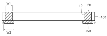
- FIG. 2 illustrates a cross-sectional view of II ′ of FIG. 1.
- Two through holes 10 are formed at both edges of the substrate 100.
- one through hole is then connected to the bus bar to be connected to the (+) electrode, and the other through hole is connected to the bus bar to be connected to the (-) electrode afterwards, and two are formed.
- the number of the through holes 10 is not limited thereto, and the number may be changed according to the structure of the solar cell.
- the width W1 of the through hole 10 may be formed to a size of 0.5mm ⁇ 3mm, preferably 1mm ⁇ 2mm.
- connection electrode 50 filling the inside of the through hole 10 is formed.
- connection electrode 50 may be formed by inserting Ag or Al paste to fill the through hole 10, and inserting molybdenum (Mo), which is a back electrode material, into the through hole 10. It may be formed to.
- Mo molybdenum
- connection electrode 50 is not limited thereto, and may be formed of a conductive material.
- bus bar 150 on the back of the substrate 100.
- the bus bar 150 may be formed to be exposed to the rear surface of the substrate 100, and may be electrically connected to the connection electrode 50.
- the bus bar 150 may be formed of a conductive material including Al and Cu.
- the bus bar 150 may be formed to have a width W2 of 1 mm to 5 mm, preferably 3 mm to 4 mm.
- the bus bar 150 may be wider than the width W1 of the connection electrode 50.
- connection electrode 50 and the bus bar 150 may be changed. That is, although the bus bar 150 is formed after the connection electrode 50 is formed in the embodiment, the bus bar 150 may be formed first, and then the connection electrode 50 may be formed.
- the back electrode pattern 200 is formed on the front surface of the substrate 100.
- the back electrode pattern 200 may be formed of a conductor such as metal.
- the back electrode pattern 200 may be formed by a sputtering process using a molybdenum (Mo) target.
- Mo molybdenum
- the back electrode pattern 200 may be formed to cover the through hole 10. That is, it may be electrically connected to the connection electrode 50.
- the back electrode pattern 200 and the bus bar 150 are electrically connected by the connection electrode 50.
- the through hole 10 is formed at an edge of the substrate 100, and the back electrode pattern 200 and the bus bar 150 formed at the outermost portion of the substrate 100 are electrically connected to each other.
- the back electrode pattern 200 may be formed of at least one layer.
- the layers constituting the back electrode pattern 200 may be formed of different materials.
- a portion of the substrate 100 may be exposed between the rear electrode patterns 200.
- the back electrode pattern 200 may be arranged in a stripe form or a matrix form and may correspond to each cell.
- the back electrode pattern 200 is not limited to the above form and may be formed in various forms.
- the back electrode pattern 200 is formed to electrically connect the back electrode pattern 200 and the bus bar 150.
- the rear electrode pattern 200 may be formed after the bus bar 150 is formed on the rear surface of the substrate 150.
- a material of the back electrode pattern 200 is formed in the through hole 10. Inserted therein, it may be electrically connected to the bus bar 150.
- a light absorbing layer 300 and a buffer layer 400 are formed on the back electrode pattern 200.
- the light absorbing layer 300 includes an Ib-IIIb-VIb-based compound.
- the light absorbing layer 300 includes a copper-indium-gallium-selenide-based (Cu (In, Ga) Se 2 , CIGS-based) compound.
- the light absorbing layer 300 may include a copper-indium selenide-based (CuInSe 2 , CIS-based) compound or a copper-gallium-selenide-based (CuGaSe 2 , CIS-based) compound.
- a CIG-based metal precursor film is formed on the back electrode pattern 200 using a copper target, an indium target, and a gallium target.
- the metal precursor film is reacted with selenium (Se) by a selenization process to form a CIGS-based light absorbing layer 300.
- Se selenium
- an alkali component included in the substrate 100 may pass through the back electrode pattern 200, and the metal precursor film and the light absorbing layer ( 300).
- An alkali component may improve grain size and improve crystallinity of the light absorbing layer 300.
- the light absorbing layer 300 may form copper, indium, gallium, selenide (Cu, In, Ga, Se) by co-evaporation.
- the light absorbing layer 300 may be formed on the back electrode pattern 200, and may be formed on the substrate 100 partially exposed between the back electrode patterns 200.
- the light absorbing layer 300 receives external light and converts the light into electrical energy.
- the light absorbing layer 300 generates photo electromotive force by the photoelectric effect.
- the buffer layer 400 is formed on the light absorbing layer 300, is formed of at least one or more layers, and cadmium sulfide (CdS), ITO, ZnO, on the substrate 100 on which the light absorbing layer 300 is formed. It may be formed of any one of i-ZnO or a stack thereof.
- the buffer layer 400 is an n-type semiconductor layer
- the light absorbing layer 300 is a p-type semiconductor layer.
- the light absorbing layer 300 and the buffer layer 400 form a pn junction.
- the buffer layer 400 is disposed between the light absorbing layer 300 and the front electrode to be formed later.
- a good junction may be formed by inserting the buffer layer 400 having a band gap between the two materials.
- one buffer layer is formed on the light absorbing layer 300, but the present invention is not limited thereto, and the buffer layer may be formed of a plurality of layers.
- a contact pattern 310 penetrating the light absorbing layer 300 and the buffer layer 400 is formed.
- the contact pattern 310 may be formed by a mechanical method, and a portion of the back electrode pattern 200 is exposed.
- the contact pattern 310 may be formed in an area adjacent to the back electrode pattern 200.
- a transparent conductive material is stacked on the buffer layer 400 to form the front electrode 500 and the connection wiring 700.
- the transparent conductive material When the transparent conductive material is stacked on the buffer layer 400, the transparent conductive material may also be inserted into the contact pattern 310 to form the connection wiring 700. That is, the front electrode 500 and the connection wiring 700 may be formed of the same material.
- the back electrode pattern 200 and the front electrode 500 are electrically connected to each other by the connection wiring 700.
- the front electrode 500 is formed of zinc oxide doped with aluminum by performing a sputtering process on the substrate 100.
- the front electrode 500 is a window layer forming a pn junction with the light absorbing layer 300. Since the front electrode 500 functions as a transparent electrode on the front of the solar cell, zinc oxide (ZnO) having high light transmittance and good electrical conductivity is provided. Is formed.
- ZnO zinc oxide
- the aluminum oxide may be doped with aluminum to form an electrode having a low resistance value.
- the zinc oxide thin film as the front electrode 500 may be formed by a method of depositing using a ZnO target by RF sputtering, reactive sputtering using a Zn target, and an organometallic chemical vapor deposition method.
- ITO indium tin oxide
- a separation pattern 320 penetrating the light absorbing layer 300, the buffer layer 400, and the front electrode 500 is formed.
- the separation pattern 320 may be formed by a mechanical method, and a part of the top surface of the back electrode pattern 200 is exposed.
- the buffer layer 400 and the front electrode 500 may be separated by the separation pattern 320, and the cells C1 and C2 may be separated from each other by the separation pattern 320.
- the front electrode 500, the buffer layer 400, and the light absorbing layer 300 may be arranged in the form of a stripe or a matrix by the separation pattern 320.
- the separation pattern 320 is not limited to the above form and may be formed in various forms.
- Cells C1 and C2 including the back electrode pattern 200, the light absorbing layer 300, the buffer layer 400, and the front electrode 500 are formed by the separation pattern 320.
- each of the cells C1 and C2 may be connected to each other by the connection wiring 700. That is, the connection wiring 700 electrically connects the back electrode pattern 200 of the second cell C2 and the front electrode 500 of the first cell C1 adjacent to the second cell C2. do.
- FIG. 10 is a plan view illustrating a front surface of the substrate 100 on which a solar cell is formed by the separation pattern 320, and FIG. 11 illustrates a rear surface of the substrate 100 on which the bus bar 150 is formed. Top view.
- bus bar 150 is formed on the rear surface of the substrate 100, a bus bar is formed on the front electrode 500 to transmit a signal of the bus bar to the rear surface of the substrate 100. It is not necessary to form additionally.
- the width W1 of the connection electrode 50 directly connected to the back electrode pattern 200 is formed to be narrower than the width W2 of the bus bar 150, thereby widening the solar cell forming region.
- the existing bus bar is formed on the front electrode 500, the solar cell forming region is narrowed by the width of the bus bar, in the present embodiment, the connection narrower than the bus bar 150 Since the electrode 50 is connected to the back electrode pattern 200, the solar cell formation region may be widened.
- the efficiency of the solar cell may also be increased.
- connection electrode having a narrower width than the bus bar is connected to the rear electrode pattern through the through hole, so that the solar cell forming region is widened, thereby increasing the efficiency of the solar cell. Can be.
Landscapes
- Photovoltaic Devices (AREA)
Abstract
Priority Applications (4)
| Application Number | Priority Date | Filing Date | Title |
|---|---|---|---|
| US13/379,300 US20120186624A1 (en) | 2009-11-03 | 2010-11-01 | Solar Cell and Manufacturing Method Thereof |
| JP2012536701A JP2013510426A (ja) | 2009-11-03 | 2010-11-01 | 太陽電池及びその製造方法 |
| CN2010800499202A CN102598302A (zh) | 2009-11-03 | 2010-11-01 | 太阳能电池及其制造方法 |
| EP10828481.1A EP2442369A4 (fr) | 2009-11-03 | 2010-11-01 | Cellule solaire et procédé de fabrication de celle-ci |
Applications Claiming Priority (2)
| Application Number | Priority Date | Filing Date | Title |
|---|---|---|---|
| KR10-2009-0105424 | 2009-11-03 | ||
| KR1020090105424A KR101125322B1 (ko) | 2009-11-03 | 2009-11-03 | 태양전지 및 이의 제조방법 |
Publications (2)
| Publication Number | Publication Date |
|---|---|
| WO2011055946A2 true WO2011055946A2 (fr) | 2011-05-12 |
| WO2011055946A3 WO2011055946A3 (fr) | 2011-09-29 |
Family
ID=43970517
Family Applications (1)
| Application Number | Title | Priority Date | Filing Date |
|---|---|---|---|
| PCT/KR2010/007616 Ceased WO2011055946A2 (fr) | 2009-11-03 | 2010-11-01 | Cellule solaire et procédé de fabrication de celle-ci |
Country Status (6)
| Country | Link |
|---|---|
| US (1) | US20120186624A1 (fr) |
| EP (1) | EP2442369A4 (fr) |
| JP (1) | JP2013510426A (fr) |
| KR (1) | KR101125322B1 (fr) |
| CN (1) | CN102598302A (fr) |
| WO (1) | WO2011055946A2 (fr) |
Cited By (3)
| Publication number | Priority date | Publication date | Assignee | Title |
|---|---|---|---|---|
| JP2013115119A (ja) * | 2011-11-25 | 2013-06-10 | Nitto Denko Corp | 化合物太陽電池セルおよびその製法ならびにそれを用いた化合物太陽電池モジュールおよびその製法 |
| US20140326291A1 (en) * | 2011-10-13 | 2014-11-06 | Lg Innotek Co., Ltd. | Solar cell module and method of fabricating the same |
| WO2015056934A1 (fr) * | 2013-10-18 | 2015-04-23 | 엘지이노텍 주식회사 | Module de cellule solaire |
Families Citing this family (10)
| Publication number | Priority date | Publication date | Assignee | Title |
|---|---|---|---|---|
| KR101470065B1 (ko) * | 2012-03-05 | 2014-12-08 | 엘지이노텍 주식회사 | 태양전지 모듈 |
| KR101459830B1 (ko) * | 2012-08-23 | 2014-11-21 | 엘지이노텍 주식회사 | 태양전지 및 이의 제조 방법 |
| WO2017103663A1 (fr) | 2015-12-15 | 2017-06-22 | Flisom Ag | Structuration d'un appareil photovoltaïque |
| EP3391418B1 (fr) * | 2015-12-15 | 2022-11-16 | Flisom AG | Barre omnibus de module solaire |
| WO2017118905A1 (fr) | 2016-01-06 | 2017-07-13 | Flisom Ag | Appareil photovoltaïque souple |
| KR102567037B1 (ko) * | 2016-01-19 | 2023-08-14 | 주성엔지니어링(주) | 박막형 태양전지 및 그 제조 방법 |
| EP3414779B1 (fr) * | 2016-02-11 | 2021-01-13 | Flisom AG | Modelage à auto-assemblage pour fabrication de dispositifs à film mince |
| CN109037368A (zh) * | 2018-08-21 | 2018-12-18 | 北京铂阳顶荣光伏科技有限公司 | 太阳能电池组件及电极引出方法 |
| CN117673194A (zh) * | 2022-09-01 | 2024-03-08 | 中国建材国际工程集团有限公司 | 一种柔性cigs太阳电池组件及其制作方法 |
| KR102715008B1 (ko) * | 2022-12-15 | 2024-10-07 | 주식회사 에스티 | 신재생에너지 생산을 위한 태양전지모듈 제조방법 |
Family Cites Families (13)
| Publication number | Priority date | Publication date | Assignee | Title |
|---|---|---|---|---|
| JPS60123073A (ja) * | 1983-12-08 | 1985-07-01 | Fuji Electric Corp Res & Dev Ltd | 薄膜太陽電池 |
| US6720576B1 (en) * | 1992-09-11 | 2004-04-13 | Semiconductor Energy Laboratory Co., Ltd. | Plasma processing method and photoelectric conversion device |
| JP2755281B2 (ja) * | 1992-12-28 | 1998-05-20 | 富士電機株式会社 | 薄膜太陽電池およびその製造方法 |
| JP3352252B2 (ja) * | 1994-11-04 | 2002-12-03 | キヤノン株式会社 | 太陽電池素子群並びに太陽電池モジュール及びその製造方法 |
| EP0986109A4 (fr) * | 1998-03-25 | 2005-01-12 | Tdk Corp | Module de batterie solaire |
| JP3424553B2 (ja) * | 1998-06-16 | 2003-07-07 | 株式会社デンソー | 横形絶縁ゲート型トランジスタ |
| JP4558646B2 (ja) * | 2003-06-19 | 2010-10-06 | 株式会社カネカ | 集積化薄膜光電変換装置 |
| JP4064340B2 (ja) * | 2003-12-25 | 2008-03-19 | 昭和シェル石油株式会社 | 集積型薄膜太陽電池の製造方法 |
| KR100682017B1 (ko) * | 2004-12-16 | 2007-02-12 | 주식회사 실트론 | 태양전지 및 이의 제작 방법 |
| US20080023065A1 (en) * | 2006-07-25 | 2008-01-31 | Borden Peter G | Thin film photovoltaic module wiring for improved efficiency |
| JP5025184B2 (ja) * | 2006-07-28 | 2012-09-12 | 京セラ株式会社 | 太陽電池素子及びこれを用いた太陽電池モジュール、並びに、これらの製造方法 |
| EP2253023B2 (fr) * | 2008-03-11 | 2022-11-09 | (CNBM) Bengbu Design & Research Institute for Glass Industry Co., Ltd. | Module solaire |
| KR100984700B1 (ko) | 2009-06-04 | 2010-10-01 | 엘지전자 주식회사 | 태양 전지 및 그 제조 방법 |
-
2009
- 2009-11-03 KR KR1020090105424A patent/KR101125322B1/ko not_active Expired - Fee Related
-
2010
- 2010-11-01 EP EP10828481.1A patent/EP2442369A4/fr not_active Withdrawn
- 2010-11-01 US US13/379,300 patent/US20120186624A1/en not_active Abandoned
- 2010-11-01 JP JP2012536701A patent/JP2013510426A/ja active Pending
- 2010-11-01 WO PCT/KR2010/007616 patent/WO2011055946A2/fr not_active Ceased
- 2010-11-01 CN CN2010800499202A patent/CN102598302A/zh active Pending
Non-Patent Citations (1)
| Title |
|---|
| None |
Cited By (4)
| Publication number | Priority date | Publication date | Assignee | Title |
|---|---|---|---|---|
| US20140326291A1 (en) * | 2011-10-13 | 2014-11-06 | Lg Innotek Co., Ltd. | Solar cell module and method of fabricating the same |
| JP2013115119A (ja) * | 2011-11-25 | 2013-06-10 | Nitto Denko Corp | 化合物太陽電池セルおよびその製法ならびにそれを用いた化合物太陽電池モジュールおよびその製法 |
| WO2015056934A1 (fr) * | 2013-10-18 | 2015-04-23 | 엘지이노텍 주식회사 | Module de cellule solaire |
| US10249770B2 (en) | 2013-10-18 | 2019-04-02 | Lg Innotek Co., Ltd. | Solar cell module |
Also Published As
| Publication number | Publication date |
|---|---|
| US20120186624A1 (en) | 2012-07-26 |
| KR101125322B1 (ko) | 2012-03-27 |
| CN102598302A (zh) | 2012-07-18 |
| EP2442369A4 (fr) | 2013-10-02 |
| JP2013510426A (ja) | 2013-03-21 |
| WO2011055946A3 (fr) | 2011-09-29 |
| KR20110048730A (ko) | 2011-05-12 |
| EP2442369A2 (fr) | 2012-04-18 |
Similar Documents
| Publication | Publication Date | Title |
|---|---|---|
| WO2011002230A2 (fr) | Batterie solaire et son procédé de production | |
| WO2011053077A2 (fr) | Cellule solaire et procédé de fabrication associé | |
| KR101125322B1 (ko) | 태양전지 및 이의 제조방법 | |
| WO2015041470A1 (fr) | Cellule solaire | |
| WO2011040782A2 (fr) | Appareil de production d'énergie solaire et procédé de fabrication correspondant | |
| WO2011043610A2 (fr) | Appareil de génération d'énergie photovoltaïque et procédé pour sa fabrication | |
| WO2011040781A2 (fr) | Appareil de génération d'énergie solaire et son procédé de fabrication | |
| WO2011040780A2 (fr) | Appareil de génération d'énergie solaire et son procédé de fabrication | |
| WO2013062298A1 (fr) | Cellule solaire et procédé de fabrication de celle-ci | |
| WO2011002211A2 (fr) | Pile solaire et procédé de production associé | |
| WO2013147517A1 (fr) | Cellule solaire et procédé de fabrication de celle-ci | |
| WO2012033274A1 (fr) | Dispositif permettant de produire de l'énergie solaire et son procédé de fabrication | |
| WO2014021617A1 (fr) | Appareil à cellules solaires et son procédé de fabrication | |
| WO2012046934A1 (fr) | Dispositif photovoltaïque et son procédé de fabrication | |
| WO2012015150A1 (fr) | Dispositif de production d'énergie photovoltaïque et procédé de fabrication associé | |
| WO2012015286A2 (fr) | Dispositif destiné à générer de l'énergie photovoltaïque et son procédé de fabrication | |
| WO2012057490A2 (fr) | Appareil à cellules solaires et son procédé de fabrication | |
| WO2013058521A1 (fr) | Cellule solaire et procédé de fabrication de celle-ci | |
| WO2013055008A1 (fr) | Cellule solaire et module de cellule solaire | |
| WO2013055005A1 (fr) | Cellule solaire et son procédé de préparation | |
| WO2011055954A2 (fr) | Batterie solaire et procédé de fabrication de celle-ci | |
| WO2011083994A2 (fr) | Dispositif photovoltaïque solaire | |
| WO2012102453A1 (fr) | Cellule solaire et procédé de fabrication de celle-ci | |
| WO2012102476A2 (fr) | Appareil à cellule solaire et son procédé de fabrication | |
| WO2011083995A2 (fr) | Dispositif photovoltaïque solaire et son procédé de fabrication |
Legal Events
| Date | Code | Title | Description |
|---|---|---|---|
| WWE | Wipo information: entry into national phase |
Ref document number: 201080049920.2 Country of ref document: CN |
|
| 121 | Ep: the epo has been informed by wipo that ep was designated in this application |
Ref document number: 10828481 Country of ref document: EP Kind code of ref document: A1 |
|
| WWE | Wipo information: entry into national phase |
Ref document number: 13379300 Country of ref document: US |
|
| WWE | Wipo information: entry into national phase |
Ref document number: 2010828481 Country of ref document: EP |
|
| WWE | Wipo information: entry into national phase |
Ref document number: 2012536701 Country of ref document: JP |
|
| NENP | Non-entry into the national phase |
Ref country code: DE |