WO2011083671A1 - 蛍光体、発光装置およびそれを用いた液晶表示装置 - Google Patents
蛍光体、発光装置およびそれを用いた液晶表示装置 Download PDFInfo
- Publication number
- WO2011083671A1 WO2011083671A1 PCT/JP2010/072684 JP2010072684W WO2011083671A1 WO 2011083671 A1 WO2011083671 A1 WO 2011083671A1 JP 2010072684 W JP2010072684 W JP 2010072684W WO 2011083671 A1 WO2011083671 A1 WO 2011083671A1
- Authority
- WO
- WIPO (PCT)
- Prior art keywords
- light emitting
- phosphor
- light
- general formula
- emitting device
- Prior art date
- Legal status (The legal status is an assumption and is not a legal conclusion. Google has not performed a legal analysis and makes no representation as to the accuracy of the status listed.)
- Ceased
Links
Images
Classifications
-
- C—CHEMISTRY; METALLURGY
- C09—DYES; PAINTS; POLISHES; NATURAL RESINS; ADHESIVES; COMPOSITIONS NOT OTHERWISE PROVIDED FOR; APPLICATIONS OF MATERIALS NOT OTHERWISE PROVIDED FOR
- C09K—MATERIALS FOR MISCELLANEOUS APPLICATIONS, NOT PROVIDED FOR ELSEWHERE
- C09K11/00—Luminescent materials, e.g. electroluminescent or chemiluminescent
- C09K11/08—Luminescent materials, e.g. electroluminescent or chemiluminescent containing inorganic luminescent materials
- C09K11/0883—Arsenides; Nitrides; Phosphides
-
- C—CHEMISTRY; METALLURGY
- C09—DYES; PAINTS; POLISHES; NATURAL RESINS; ADHESIVES; COMPOSITIONS NOT OTHERWISE PROVIDED FOR; APPLICATIONS OF MATERIALS NOT OTHERWISE PROVIDED FOR
- C09K—MATERIALS FOR MISCELLANEOUS APPLICATIONS, NOT PROVIDED FOR ELSEWHERE
- C09K11/00—Luminescent materials, e.g. electroluminescent or chemiluminescent
- C09K11/08—Luminescent materials, e.g. electroluminescent or chemiluminescent containing inorganic luminescent materials
- C09K11/64—Luminescent materials, e.g. electroluminescent or chemiluminescent containing inorganic luminescent materials containing aluminium
-
- H—ELECTRICITY
- H10—SEMICONDUCTOR DEVICES; ELECTRIC SOLID-STATE DEVICES NOT OTHERWISE PROVIDED FOR
- H10H—INORGANIC LIGHT-EMITTING SEMICONDUCTOR DEVICES HAVING POTENTIAL BARRIERS
- H10H20/00—Individual inorganic light-emitting semiconductor devices having potential barriers, e.g. light-emitting diodes [LED]
- H10H20/80—Constructional details
- H10H20/85—Packages
- H10H20/851—Wavelength conversion means
- H10H20/8511—Wavelength conversion means characterised by their material, e.g. binder
- H10H20/8512—Wavelength conversion materials
- H10H20/8513—Wavelength conversion materials having two or more wavelength conversion materials
-
- C—CHEMISTRY; METALLURGY
- C09—DYES; PAINTS; POLISHES; NATURAL RESINS; ADHESIVES; COMPOSITIONS NOT OTHERWISE PROVIDED FOR; APPLICATIONS OF MATERIALS NOT OTHERWISE PROVIDED FOR
- C09K—MATERIALS FOR MISCELLANEOUS APPLICATIONS, NOT PROVIDED FOR ELSEWHERE
- C09K11/00—Luminescent materials, e.g. electroluminescent or chemiluminescent
- C09K11/08—Luminescent materials, e.g. electroluminescent or chemiluminescent containing inorganic luminescent materials
- C09K11/59—Luminescent materials, e.g. electroluminescent or chemiluminescent containing inorganic luminescent materials containing silicon
-
- C—CHEMISTRY; METALLURGY
- C09—DYES; PAINTS; POLISHES; NATURAL RESINS; ADHESIVES; COMPOSITIONS NOT OTHERWISE PROVIDED FOR; APPLICATIONS OF MATERIALS NOT OTHERWISE PROVIDED FOR
- C09K—MATERIALS FOR MISCELLANEOUS APPLICATIONS, NOT PROVIDED FOR ELSEWHERE
- C09K11/00—Luminescent materials, e.g. electroluminescent or chemiluminescent
- C09K11/08—Luminescent materials, e.g. electroluminescent or chemiluminescent containing inorganic luminescent materials
- C09K11/77—Luminescent materials, e.g. electroluminescent or chemiluminescent containing inorganic luminescent materials containing rare earth metals
-
- C—CHEMISTRY; METALLURGY
- C09—DYES; PAINTS; POLISHES; NATURAL RESINS; ADHESIVES; COMPOSITIONS NOT OTHERWISE PROVIDED FOR; APPLICATIONS OF MATERIALS NOT OTHERWISE PROVIDED FOR
- C09K—MATERIALS FOR MISCELLANEOUS APPLICATIONS, NOT PROVIDED FOR ELSEWHERE
- C09K11/00—Luminescent materials, e.g. electroluminescent or chemiluminescent
- C09K11/08—Luminescent materials, e.g. electroluminescent or chemiluminescent containing inorganic luminescent materials
- C09K11/77—Luminescent materials, e.g. electroluminescent or chemiluminescent containing inorganic luminescent materials containing rare earth metals
- C09K11/7728—Luminescent materials, e.g. electroluminescent or chemiluminescent containing inorganic luminescent materials containing rare earth metals containing europium
- C09K11/77348—Silicon Aluminium Nitrides or Silicon Aluminium Oxynitrides
-
- G—PHYSICS
- G02—OPTICS
- G02F—OPTICAL DEVICES OR ARRANGEMENTS FOR THE CONTROL OF LIGHT BY MODIFICATION OF THE OPTICAL PROPERTIES OF THE MEDIA OF THE ELEMENTS INVOLVED THEREIN; NON-LINEAR OPTICS; FREQUENCY-CHANGING OF LIGHT; OPTICAL LOGIC ELEMENTS; OPTICAL ANALOGUE/DIGITAL CONVERTERS
- G02F1/00—Devices or arrangements for the control of the intensity, colour, phase, polarisation or direction of light arriving from an independent light source, e.g. switching, gating or modulating; Non-linear optics
- G02F1/01—Devices or arrangements for the control of the intensity, colour, phase, polarisation or direction of light arriving from an independent light source, e.g. switching, gating or modulating; Non-linear optics for the control of the intensity, phase, polarisation or colour
- G02F1/13—Devices or arrangements for the control of the intensity, colour, phase, polarisation or direction of light arriving from an independent light source, e.g. switching, gating or modulating; Non-linear optics for the control of the intensity, phase, polarisation or colour based on liquid crystals, e.g. single liquid crystal display cells
- G02F1/133—Constructional arrangements; Operation of liquid crystal cells; Circuit arrangements
- G02F1/1333—Constructional arrangements; Manufacturing methods
- G02F1/1335—Structural association of cells with optical devices, e.g. polarisers or reflectors
-
- G—PHYSICS
- G02—OPTICS
- G02F—OPTICAL DEVICES OR ARRANGEMENTS FOR THE CONTROL OF LIGHT BY MODIFICATION OF THE OPTICAL PROPERTIES OF THE MEDIA OF THE ELEMENTS INVOLVED THEREIN; NON-LINEAR OPTICS; FREQUENCY-CHANGING OF LIGHT; OPTICAL LOGIC ELEMENTS; OPTICAL ANALOGUE/DIGITAL CONVERTERS
- G02F1/00—Devices or arrangements for the control of the intensity, colour, phase, polarisation or direction of light arriving from an independent light source, e.g. switching, gating or modulating; Non-linear optics
- G02F1/01—Devices or arrangements for the control of the intensity, colour, phase, polarisation or direction of light arriving from an independent light source, e.g. switching, gating or modulating; Non-linear optics for the control of the intensity, phase, polarisation or colour
- G02F1/13—Devices or arrangements for the control of the intensity, colour, phase, polarisation or direction of light arriving from an independent light source, e.g. switching, gating or modulating; Non-linear optics for the control of the intensity, phase, polarisation or colour based on liquid crystals, e.g. single liquid crystal display cells
- G02F1/133—Constructional arrangements; Operation of liquid crystal cells; Circuit arrangements
- G02F1/1333—Constructional arrangements; Manufacturing methods
- G02F1/1335—Structural association of cells with optical devices, e.g. polarisers or reflectors
- G02F1/1336—Illuminating devices
-
- G—PHYSICS
- G02—OPTICS
- G02F—OPTICAL DEVICES OR ARRANGEMENTS FOR THE CONTROL OF LIGHT BY MODIFICATION OF THE OPTICAL PROPERTIES OF THE MEDIA OF THE ELEMENTS INVOLVED THEREIN; NON-LINEAR OPTICS; FREQUENCY-CHANGING OF LIGHT; OPTICAL LOGIC ELEMENTS; OPTICAL ANALOGUE/DIGITAL CONVERTERS
- G02F1/00—Devices or arrangements for the control of the intensity, colour, phase, polarisation or direction of light arriving from an independent light source, e.g. switching, gating or modulating; Non-linear optics
- G02F1/01—Devices or arrangements for the control of the intensity, colour, phase, polarisation or direction of light arriving from an independent light source, e.g. switching, gating or modulating; Non-linear optics for the control of the intensity, phase, polarisation or colour
- G02F1/13—Devices or arrangements for the control of the intensity, colour, phase, polarisation or direction of light arriving from an independent light source, e.g. switching, gating or modulating; Non-linear optics for the control of the intensity, phase, polarisation or colour based on liquid crystals, e.g. single liquid crystal display cells
- G02F1/133—Constructional arrangements; Operation of liquid crystal cells; Circuit arrangements
- G02F1/1333—Constructional arrangements; Manufacturing methods
- G02F1/1335—Structural association of cells with optical devices, e.g. polarisers or reflectors
- G02F1/1336—Illuminating devices
- G02F1/133602—Direct backlight
- G02F1/133603—Direct backlight with LEDs
-
- H—ELECTRICITY
- H10—SEMICONDUCTOR DEVICES; ELECTRIC SOLID-STATE DEVICES NOT OTHERWISE PROVIDED FOR
- H10H—INORGANIC LIGHT-EMITTING SEMICONDUCTOR DEVICES HAVING POTENTIAL BARRIERS
- H10H20/00—Individual inorganic light-emitting semiconductor devices having potential barriers, e.g. light-emitting diodes [LED]
- H10H20/80—Constructional details
- H10H20/85—Packages
- H10H20/851—Wavelength conversion means
- H10H20/8511—Wavelength conversion means characterised by their material, e.g. binder
- H10H20/8512—Wavelength conversion materials
-
- H—ELECTRICITY
- H10—SEMICONDUCTOR DEVICES; ELECTRIC SOLID-STATE DEVICES NOT OTHERWISE PROVIDED FOR
- H10W—GENERIC PACKAGES, INTERCONNECTIONS, CONNECTORS OR OTHER CONSTRUCTIONAL DETAILS OF DEVICES COVERED BY CLASS H10
- H10W90/00—Package configurations
- H10W90/701—Package configurations characterised by the relative positions of pads or connectors relative to package parts
- H10W90/751—Package configurations characterised by the relative positions of pads or connectors relative to package parts of bond wires
- H10W90/756—Package configurations characterised by the relative positions of pads or connectors relative to package parts of bond wires between a chip and a stacked lead frame, conducting package substrate or heat sink
-
- Y—GENERAL TAGGING OF NEW TECHNOLOGICAL DEVELOPMENTS; GENERAL TAGGING OF CROSS-SECTIONAL TECHNOLOGIES SPANNING OVER SEVERAL SECTIONS OF THE IPC; TECHNICAL SUBJECTS COVERED BY FORMER USPC CROSS-REFERENCE ART COLLECTIONS [XRACs] AND DIGESTS
- Y10—TECHNICAL SUBJECTS COVERED BY FORMER USPC
- Y10T—TECHNICAL SUBJECTS COVERED BY FORMER US CLASSIFICATION
- Y10T428/00—Stock material or miscellaneous articles
- Y10T428/29—Coated or structually defined flake, particle, cell, strand, strand portion, rod, filament, macroscopic fiber or mass thereof
- Y10T428/2982—Particulate matter [e.g., sphere, flake, etc.]
Definitions
- the present invention relates to a phosphor suitable for a light emitting device, a light emitting device using the same for a wavelength conversion unit, particularly a light emitting device having stable characteristics, and a liquid crystal display using the same.
- a light emitting device combining a semiconductor light emitting element and a phosphor has attracted attention as a next-generation light emitting device expected to have low power consumption, small size, high luminance, wide range color reproducibility, and high color rendering. ⁇ Development is under way.
- the primary light emitted from the light emitting element is usually in the range of long wavelength ultraviolet light to blue, ie, 380 to 480 nm.
- wavelength converters using various phosphors adapted to this application have also been proposed.
- a blue light emitting element peak wavelength: around 460 nm
- trivalent cerium which is excited by the blue color and shows yellow light emission is activated (Y, Gd) 3
- Y, Gd A combination of Al, Ga) 5 O 12 phosphor or 2 (Sr, Ba) O ⁇ SiO 2 phosphor activated with divalent europium is mainly used.
- the color reproducibility is around 70%, and in recent years, even in a small LCD, a device with better color reproducibility is required.
- the divalent europium-activated oxynitride green light emitting phosphor that is ⁇ -type SiAlON is basically a columnar crystal, and if it is intended to maintain its crystal structure in a simple composition, a sintered body (Aggregates) are easily generated.
- the extremely large columnar crystals (needle-like crystals) have insufficient crystal growth, and good characteristics (brightness) can not be obtained.
- the sintered body (aggregate) is not a single uniform particle, good characteristics (brightness) can not be obtained for the size due to absorption of light at grain boundaries and the like.
- JP-A-2005-255895 Patent Document 1 relates to ⁇ -type SiAlON in which the crystal phase is a single crystal having an average particle diameter of 50 nm or more and 20 ⁇ m or less, or the average particle diameter of the synthesized phosphor powder is 50 nm It is described that the particle size is adjusted to 20 ⁇ m or less.
- Patent Document 1 does not describe the dispersibility (degree of aggregation (sintering)), nor describes the relationship between it and the absorptivity at 600 nm, and further, the initial characteristics and life characteristics of the light emitting device.
- the present invention has been made to solve the above problems, and the object of the present invention is to stabilize the characteristics with high efficiency by using the ⁇ -type SiAlON whose dispersibility is controlled and transparency is enhanced. Providing a light emitting device.
- the present inventors not only depend on the optimization of the chemical composition of ⁇ -type SiAlON, but also to improve the dispersibility of the particles. It has been found that a light emitting device having excellent initial characteristics (brightness) and good life characteristics can be obtained by using the ⁇ -type SiAlON. That is, the present invention is as follows.
- the average particle size (d1) air permeation method
- the median diameter (50% D) in the particle size distribution is 12.5 to 35 ⁇ m.
- the green light emitting phosphor of the present invention preferably has c ⁇ 0.3 in the general formula (A).
- the green light emitting phosphor of the present invention in the general formula (A), it is preferable that 0.01 ⁇ a ⁇ 0.2.
- the present invention also relates to a light emitting element which is a gallium nitride based semiconductor emitting a primary light having a peak wavelength of 430 to 480 nm, and a secondary light having a wavelength longer than that of the primary light by absorbing a part of the primary light.
- a light emitting element which is a gallium nitride based semiconductor emitting a primary light having a peak wavelength of 430 to 480 nm, and a secondary light having a wavelength longer than that of the primary light by absorbing a part of the primary light.
- the green light emitting phosphor in the light emitting device of the present invention preferably has c ⁇ 0.3 in the general formula (A).
- the green light emitting phosphor in the light emitting device of the present invention is preferably 0.01 ⁇ a ⁇ 0.2 in the general formula (A).
- a red light emitting phosphor is used in combination with the wavelength converting portion, and as the red light emitting phosphor, a general formula (B): (MI 1-x Eu x ) MIISiN 3 (In the general formula (B), MI represents at least one alkaline earth metal element selected from Mg, Ca, Sr and Ba, and MII represents Al, Ga, In, Sc, Y, La, Gd And Lu at least one trivalent metal element selected from the group consisting of: and a number satisfying 0.001 ⁇ x ⁇ 0.10. It is preferable to use a system light emitting phosphor.
- MII is preferably at least one element selected from Al, Ga and In.
- the present invention also provides a backlight source device including a plurality of the above-described light emitting devices of the present invention as point light sources.
- the present invention also provides a liquid crystal display device comprising a liquid crystal panel and the above-described backlight source device of the present invention disposed on the back of the liquid crystal panel.
- a light emitting device capable of efficiently absorbing primary light from a light emitting element and obtaining white light having high efficiency and excellent color reproducibility (NTSC ratio) and further excellent life characteristics; It is possible to provide a phosphor suitably used.
- the phosphor of the present invention is a divalent europium-activated oxynitride green light-emitting phosphor that is ⁇ -type SiAlON (sialon) represented by the following general formula (A).
- the average particle size (d1) (air permeation method) of the phosphor of the present invention is 9 to 16 ⁇ m. If d1 is less than 9 ⁇ m, many columnar crystals (needle-like crystals) and sintered bodies (aggregates) with insufficient crystal growth exist, and sufficient brightness can not be obtained. On the other hand, when d1 exceeds 16 ⁇ m, the presence of coarse sintered bodies (aggregates) increases, and sufficient brightness can not be obtained in proportion to the size. It is preferable that 10 ⁇ m ⁇ d1 ⁇ 13 ⁇ m from the stability of properties and the homogeneity of the matrix.
- the formula 50% D / d1 (that is, an index indicating the existence ratio of single particles) representing the dispersibility of crystals is limited to the range of 1.4 to 2.2.
- the 50% D / d1 is ideally 1.0, but when the 50% D / d1 is less than 1.4, the pulverization tends to be excessive and the decrease in brightness can not be ignored.
- 50% D / d1 exceeds 2.2, the presence of a sintered body (aggregate) increases, and the brightness significantly decreases. From the viewpoint of the stability of properties and the homogeneity of the mother, it is preferable to satisfy 1.6 ⁇ 50% D / d1 ⁇ 2.0.
- the average particle size (d1) air permeation method
- the range of 50% D / d1 are determined
- the median diameter (50% D) in the particle size distribution is determined accordingly. That is, it has a range of 12.5 to 35 ⁇ m.
- the body color is a ⁇ -type SiAlON (sialon) having an average particle size (d1) (air permeation method) and a range of 50% D / d1
- the absorptivity at 600 nm has a value of less than or equal to 8.0%. If it exceeds 8.0%, the absorption of long wavelength components (particularly, reddish region) can not be ignored, and the brightness of white drops significantly. It is preferable that the absorptivity at 600 nm is 7.0% or less from the viewpoint of the stability of properties and the homogeneity of the matrix.
- divalent europium-activated oxynitride green light emitting phosphor that is ⁇ -type SiAlON (Sialon) represented by the above formula are Eu 0.05 Si 11.50 Al 0.50 O 0.30 N 15.70 , and Eu 0.10 Si.
- the average particle size (d1) (air permeation method) refers to the value measured by the Lenaas method, the brain method, etc., using, for example, an air permeation type powder specific surface area measuring device (made by Tsutsui Rikagaku Instruments Co., Ltd.) Can be measured.
- the median diameter (50% D) indicates a value measured using a particle size distribution measuring apparatus (LA-920, manufactured by Horiba, Ltd.).
- LA-920 manufactured by Horiba, Ltd.
- an electrolyte sodium hexametaphosphate
- preliminary dispersion by ultrasonic waves was not performed.
- the absorptivity at 600 nm can be measured, for example, using a spectrum measurement apparatus MCPD7000 (manufactured by Otsuka Electronics Co., Ltd.).
- the phosphor of the present invention can be produced by a conventionally known appropriate method.
- the Al concentration (c) is made 0.3 or more, the oxygen concentration is accurately controlled, the density and bulk of the raw materials in the firing vessel are accurately controlled, the synthesis is performed There is a method such as optimizing the temperature profile at the time, but it is not limited thereto.
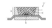
- FIG. 1 is a cross-sectional view schematically showing a light emitting device 11 according to a preferred example of the present invention.
- a gallium nitride (GaN) based semiconductor is used for the light emitting element 12 used in the light emitting device 11 of the present invention of the example shown in FIG. 1 from the viewpoint of efficiency.
- GaN gallium nitride
- the light emitting element 12 in the light emitting device 11 of the present invention one emitting primary light having a peak wavelength in the range of 430 to 480 nm is used.
- the wavelength conversion unit 13 contains the above-described phosphor of the present invention, absorbs a part of the primary light emitted from the light emitting element 12, and has a length equal to or longer than the wavelength of the primary light.
- the medium 15 is not particularly limited as long as secondary light having a wavelength can be emitted.
- a transparent resin such as an epoxy resin, a silicone resin, or a urea resin can be used, but it is not limited thereto.
- a thermosetting silicone resin encapsulant or the like is suitably used as the medium 15.
- the wavelength conversion portion 13 may of course contain appropriate additives such as SiO 2 , TiO 2 , ZrO 2 , Al 2 O 3 , Y 2 O 3 and the like within the range that does not inhibit the effects of the present invention. .
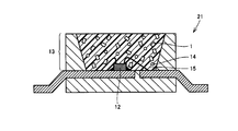
- FIG. 2 is a cross-sectional view schematically showing a light emitting device 21 according to another preferable example of the present invention.
- the wavelength conversion unit 13 of the light emitting device 21 of the present invention may of course include the phosphor 14 other than the above-described phosphor 1 of the present invention.
- the other phosphors 14 which may be included in the wavelength conversion unit 13 other than the phosphor 1 of the present invention are not particularly limited, but the phosphor 1 of the present invention is formed of a green light emitting phosphor Therefore, from the viewpoint of realizing a light emitting device exhibiting white light by color mixing, a divalent europium-activated nitride red light emitting phosphor represented by the following general formula (B) is preferable.
- MI represents at least one alkaline earth metal element selected from Mg, Ca, Sr and Ba.
- MII represents at least one trivalent metal element selected from Al, Ga, In, Sc, Y, La, Gd and Lu. Among them, MII is preferably at least one element selected from Al, Ga, and In, because red light can be emitted more efficiently.
- the value of x is preferably 0.001 ⁇ x ⁇ 0.10, and preferably 0.005 ⁇ x ⁇ 0.05. When the value of x is less than 0.001, sufficient brightness tends not to be obtained, and when the value of x exceeds 0.10, the brightness tends to be greatly reduced due to concentration quenching and the like. It is for.
- the mixing ratio with the phosphor of the present invention in the wavelength conversion unit 13 is not particularly limited.
- the ratio by weight of the phosphor is preferably in the range of 1 to 35%, and more preferably in the range of 5 to 25%.
- the wavelength conversion portion 13 in the light emitting device 11 of the present invention is a phosphor other than the phosphor of the present invention other than the above-described divalent europium-activated nitride red light emitting phosphor within the range not inhibiting the effects of the present invention. Of course, it may be included. Further, the phosphor of the present invention and the phosphor other than the above-mentioned divalent europium-activated nitride red light-emitting phosphor are the phosphor of the present invention and the above-mentioned divalent europium-activated nitride red color In addition to the light emitting phosphor, it may be further included in the wavelength conversion unit 13.
- a gallium nitride (GaN) based semiconductor is used for the light emitting element 12 used for the light emitting device 21 of the present invention from the viewpoint of efficiency. Further, as the light emitting element 12 in the light emitting device 21 of the present invention, one emitting primary light having a peak wavelength in the range of 430 to 480 nm is used. When a light emitting element having a peak wavelength of less than 430 nm is used, the contribution of the blue component is small and the color rendering property is deteriorated, which is not practical. When a light emitting element having a peak wavelength of more than 480 nm is used The brightness in white is reduced, which is not practical. From the viewpoint of efficiency, the light emitting element 12 in the light emitting device 21 of the present invention preferably emits primary light in the range of 440 to 470 nm.
- the light emitting devices 11 and 21 of the present invention can be manufactured by a conventionally known appropriate method, and the manufacturing method is not particularly limited.
- a thermosetting silicone resin sealing material is used as the medium 15, and the phosphor 1 of the present invention (and the phosphor 14 other than the phosphor of the present invention, if necessary) is kneaded with the encapsulant. Is sealed, molded and manufactured.
- the present invention also provides a backlight source device including a plurality of the above-described light emitting devices of the present invention as point light sources.
- the present invention further provides a liquid crystal display device comprising a liquid crystal panel and the above-described backlight source device of the present invention disposed on the back of the liquid crystal panel.
- a liquid crystal display device of the present invention for example, a plurality of light emitting devices are prepared, a direct type backlight light source device mounted in a matrix on a housing is disposed, and an optical sheet and a liquid crystal panel are disposed on the backlight light source device. Is configured.
- a plurality of the light emitting devices of the present invention described above are prepared, disposed on the side surface of the light guide plate, a reflecting plate is installed on the back surface of the light guide plate, and light is extracted from the surface It may be replaced with an edge light type backlight source device of
- Example 1 As a light emitting element, a gallium nitride (GaN) based semiconductor having a peak wavelength of 450 nm was used.
- this fluorescent substance is mainly prepared by controlling Al concentration (c) to 0.50.
- This phosphor is dispersed and dispersed in a thermosetting silicone resin sealing material as a medium at a predetermined ratio, and the light emitting element is sealed to prepare a wavelength conversion unit, Example 1
- the light emitting device of The brightness in the initial stage and after 5000 hours was measured for the light emitting device of Example 1 produced in this manner.
- the brightness was turned on at a forward current (IF) of 30 mA, and the light output (photocurrent) from the light emitting device was measured.
- IF forward current
- Example 1 The results of Example 1 and Comparative Example 1 are shown in Table 1. It can be seen from Table 1 that the light emitting device of Example 1 is significantly brighter and has less variation in brightness as compared with the light emitting device of Comparative Example 1.
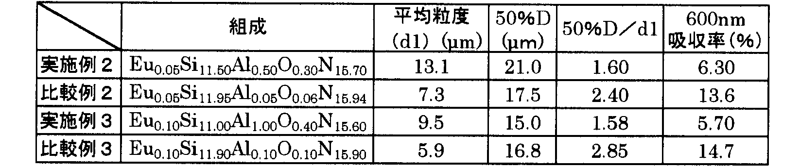
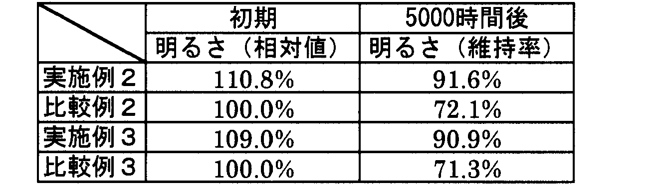
- Examples 2, 3 and Comparative Examples 2, 3> In the same manner as in Example 1 except that phosphors having various average particle sizes (d1), median diameters (50% D), 50% D / d1 values, and absorbances at 600 nm as shown in Table 2 were used. The light emitting devices of Examples 2 and 3 and Comparative Examples 2 and 3 were produced. The results of the characteristics (brightness) measured in the same manner as in Example 1 are shown in Table 3. It can be seen from Table 3 that the light emitting devices of Examples 2 and 3 are significantly brighter and have less variation in brightness than the light emitting devices of Comparative Examples 2 and 3.
- Example 4 Comparative Example 4 As a light emitting element, a gallium nitride (GaN) based semiconductor having a peak wavelength at 460 nm was used.
- the phosphor and the red light emitting phosphor are dispersed and dispersed in a thermosetting silicone resin sealing material as a medium at a predetermined ratio, and the light emitting element is sealed to obtain a wavelength conversion portion.
- the light emitting device of Example 4 was produced. With respect to the light emitting device of Example 4 produced in this manner, the brightness and the chromaticity after the initial time and 5000 hours were measured. The brightness was turned on at a forward current (IF) of 30 mA, the light output (photocurrent) from the light-emitting device was measured, and the chromaticity was measured using MCPD-2000 (manufactured by Otsuka Electronics Co., Ltd.).
- Example 4 The characteristics (brightness and chromaticity) of the light emitting devices of Example 4 and Comparative Example 4 were evaluated in the same manner as in Example 1. The results are shown in Table 4. It can be seen from Table 4 that the light emitting device of Example 4 is significantly brighter and has less variation in brightness and chromaticity as compared with the light emitting device of Comparative Example 4.
- Example 4 and Example 4 were used except that ⁇ -type SiAlON phosphors having various average particle sizes (d1), median diameters (50% D), 50% D / d 1 values, and absorptions at 600 nm as shown in Table 5 were used. Similarly, light emitting devices of Examples 5 to 9 and Comparative Examples 5 to 9 were produced. The evaluation results of the characteristics (brightness and chromaticity) measured in the same manner as in Example 4 are shown in Table 6. From Table 6, it can be seen that the light emitting devices of Examples 5 to 9 are significantly brighter and have smaller variations in brightness and chromaticity as compared with the light emitting devices of Comparative Examples 5 to 9.
- the light emitting device of the present invention is provided with a wavelength converter including the phosphor of the present invention.
- a wavelength converter including the phosphor of the present invention can efficiently absorb primary light from a light-emitting element and obtain white light of high efficiency and excellent color reproducibility (NTSC ratio), and further, good temperature and life characteristics. it can.
- a plurality of light emitting devices listed in any of the above Examples 1 to 9 are prepared, and a direct type backlight light emitting device mounted in a matrix on a casing is configured, and an optical sheet and a liquid crystal panel are formed on the backlight light source device.
- the liquid crystal display (TV) which comprised and was comprised was comprised, the liquid crystal display excellent in color reproducibility was obtained.
- a plurality of light emitting devices listed in Examples 1 to 9 are prepared, disposed on the side surface of the light guide plate, and a reflection plate is provided on the back surface of the light guide plate It may be replaced by an edge light type backlight source device configured to extract light from the surface.
Landscapes
- Chemical & Material Sciences (AREA)
- Physics & Mathematics (AREA)
- Inorganic Chemistry (AREA)
- Engineering & Computer Science (AREA)
- Materials Engineering (AREA)
- Organic Chemistry (AREA)
- Nonlinear Science (AREA)
- Mathematical Physics (AREA)
- Crystallography & Structural Chemistry (AREA)
- General Physics & Mathematics (AREA)
- Optics & Photonics (AREA)
- Luminescent Compositions (AREA)
- Led Device Packages (AREA)
- Liquid Crystal (AREA)
- Devices For Indicating Variable Information By Combining Individual Elements (AREA)
Abstract
Description
本発明の緑色系発光蛍光体は、一般式(A)中、0.01≦a≦0.2であることが好ましい。
上記一般式(A)中、aの値は、0.005≦a≦0.4であり、b+c=12であり、d+e=16である。上記一般式(A)中、aの値が0.005未満であると、十分な明るさが得られないという不具合があり、またaの値が0.4を超えると、濃度消光などにより、明るさが大きく低下するという不具合がある。なお、特性の安定性、母体の均質性から、上記一般式(A)中のaの値は、0.01≦a≦0.2であるのが好ましい。
上記一般式(B)中、MIはMg、Ca、SrおよびBaから選ばれる少なくとも1種のアルカリ土類金属元素を示す。また上記一般式(B)中、MIIはAl、Ga、In、Sc、Y、La、GdおよびLuから選ばれる少なくとも1種の3価の金属元素を示す。中でも、より一層高効率に赤色光を発光することができることから、MIIはAl、GaおよびInから選ばれる少なくとも1種の元素であることが好ましい。また上記一般式(B)中、xの値は、0.001≦x≦0.10であり、0.005≦x≦0.05であるのが好ましい。xの値が0.001未満であると、十分な明るさが得られない傾向にあり、xの値が0.10を超えると、濃度消光などにより、明るさが大きく低下するという傾向にあるためである。
発光素子として、450nmにピーク波長を有する窒化ガリウム(GaN)系半導体を用いた。波長変換部には、Eu0.05Si11.55Al0.45O0.35N15.65(β型SiAlON)なる組成を有する緑色系発光蛍光体であり、平均粒度(d1)が11.3μm、メディアン径(50%D)が18.6μm、50%D/d1=1.65、600nmにおける吸収率が5.9%である特性値を有するものを用いた。なお、この蛍光体は主として、Al濃度(c)を0.50に制御することによって、調製されたものである。この蛍光体を、所定の割合にて媒質としての熱硬化型のシリコーン樹脂製の封止材中に分散させて分散し、発光素子を封止して、波長変換部を作製し、実施例1の発光装置を作製した。このようにして作製した実施例1の発光装置について、初期および5000時間後の明るさを測定した。なお、明るさは順電流(IF)30mAにて点灯し、発光装置からの光出力(光電流)を測定した。
表2に示すような種々の平均粒度(d1)、メディアン径(50%D)、50%D/d1値、600nmにおける吸収率を有する蛍光体を用いたこと以外は実施例1と同様にして、それぞれ実施例2、3、比較例2、3の発光装置を作製した。実施例1と同様にして測定した特性(明るさ)の結果を表3に示す。表3から、実施例2、3の発光装置は、比較例2、3の発光装置に比し、著しく明るくかつ明るさの変動が小さいことが分かる。
発光素子として、460nmにピーク波長を有する窒化ガリウム(GaN)系半導体を用いた。波長変換部には、Eu0.05Si11.55Al0.45O0.35N15.65(β型SiAlON)なる組成を有する緑色系発光蛍光体であり、平均粒度(d1)が11.3μm、メディアン径(50%D)が18.6μm、50%D/d1=1.65、600nmにおける吸収率が5.9%である特性値を有するものと、(Ca0.99Eu0.01)AlSiN3(D50値:12.8μm)なる組成を有する2価のユーロピウム付活窒化物赤色系発光蛍光体とを用いた。この蛍光体および赤色系発光蛍光体を、所定の割合にて媒質としての熱硬化型のシリコーン樹脂製の封止材中に分散させて分散し、発光素子を封止して、波長変換部を作製し、実施例4の発光装置を作製した。このようにして作製した実施例4の発光装置について、初期および5000時間後の明るさおよび色度を測定した。なお、明るさは順電流(IF)30mAにて点灯し、発光装置からの光出力(光電流)を測定し、色度はMCPD-2000(大塚電子製)を用い、測定した。
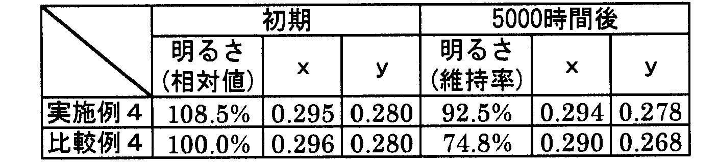
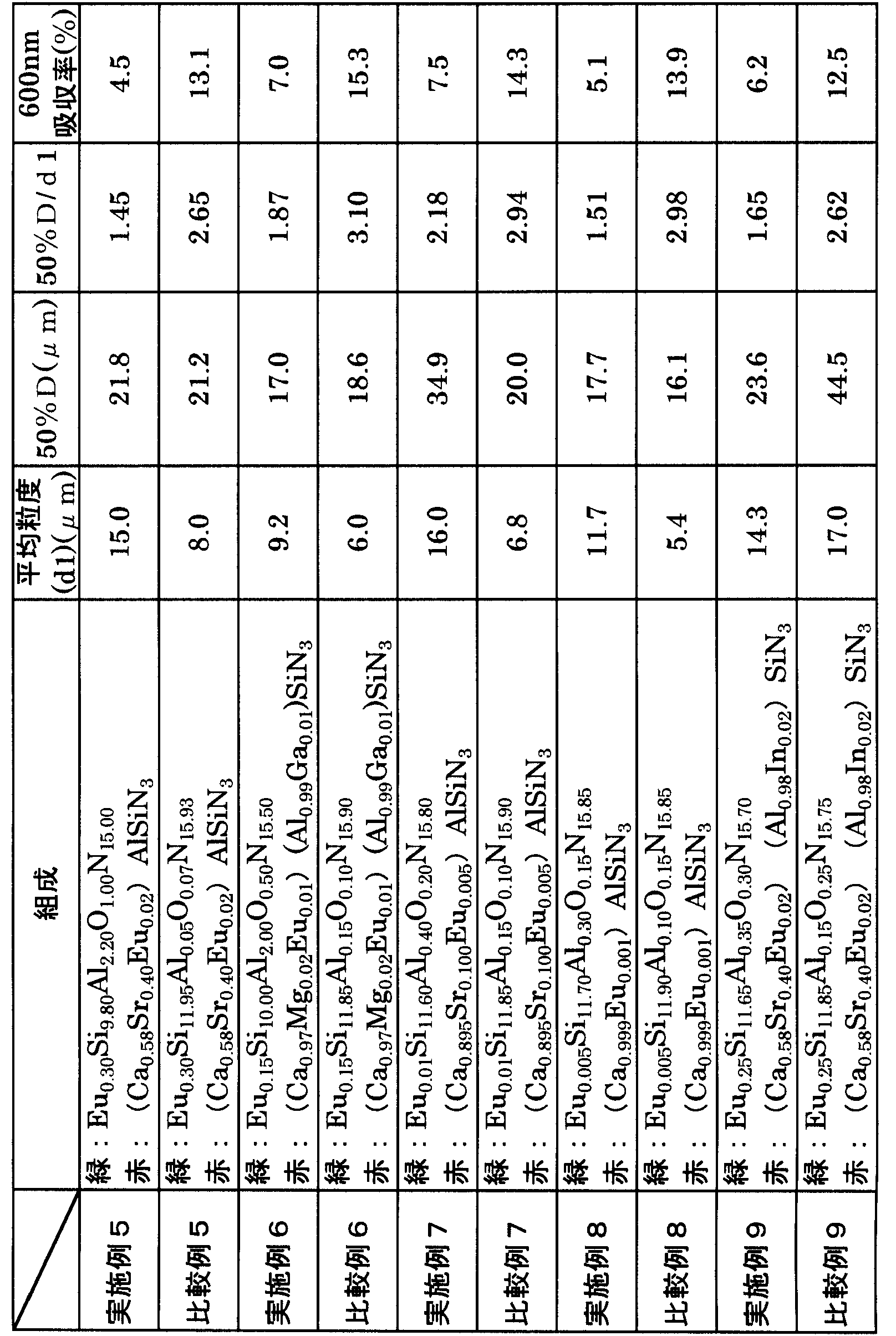
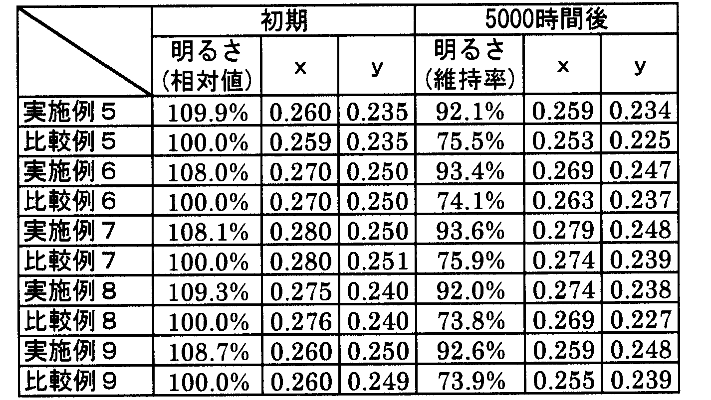
表5に示すような種々の平均粒度(d1)、メディアン径(50%D)、50%D/d1値、600nmにおける吸収率を有するβ型SiAlON蛍光体を用いたこと以外は実施例4と同様にして、それぞれ実施例5~9、比較例5~9の発光装置を作製した。実施例4と同様にして測定した特性(明るさおよび色度)の評価結果を表6に示す。表6から、実施例5~9の発光装置は、比較例5~9の発光装置に比し、著しく明るく、かつ明るさおよび色度の変動が小さいことが分かる。
Claims (12)
- 一般式(A):EuaSibAlcOdNe
(一般式(A)中、0.005≦a≦0.4、b+c=12、d+e=16を満足する数である。)
で実質的に表され、平均粒度(d1)(空気透過法)が9~16μmであり、粒度分布でのメディアン径(50%D)が12.5~35μmであり、50%D/d1=1.4~2.2であり、かつ600nmにおける吸収率が8.0%以下であるβ型SiAlONである、2価のユーロピウム付活酸窒化物緑色系発光蛍光体。 - 10μm≦d1≦13μm、50%D/d1=1.6~2.0かつ600nmにおける吸収率が7.0%以下である、請求項1に記載の蛍光体。
- 一般式(A)中、c≧0.3である、請求項1に記載の蛍光体。
- 一般式(A)中、0.01≦a≦0.2である、請求項1に記載の蛍光体。
- ピーク波長が430~480nmの一次光を発する窒化ガリウム系半導体である発光素子と、前記一次光の一部を吸収して、一次光の波長よりも長い波長を有する二次光を発する波長変換部とを備えた発光装置であって、前記波長変換部は、
一般式(A):EuaSibAlcOdNe
(一般式(A)中、0.005≦a≦0.4、b+c=12、d+e=16を満足する数である。)
で実質的に表され、平均粒度(d1)(空気透過法)が9~16μmであり、粒度分布でのメディアン径(50%D)が12.5~35μmであり、50%D/d1=1.4~2.2であり、かつ600nmにおける吸収率が8.0%以下であるβ型SiAlONである、2価のユーロピウム付活酸窒化物緑色系発光蛍光体を含む、発光装置。 - 蛍光体が、10μm≦d1≦13μm、50%D/d1=1.6~2.0かつ600nmにおける吸収率が7.0%以下である、請求項5に記載の発光装置。
- 一般式(A)中、c≧0.3である、請求項5に記載の発光装置。
- 一般式(A)中、0.01≦a≦0.2である、請求項5に記載の発光装置。
- 一般式(B):(MI1-xEux)MIISiN3
(一般式(B)中、MIはMg、Ca、SrおよびBaから選ばれる少なくとも1種のアルカリ土類金属元素を示し、MIIはAl、Ga、In、Sc、Y、La、GdおよびLuから選ばれる少なくとも1種の3価の金属元素を示し、0.001≦x≦0.10を満足する数である。)
で実質的に表される2価のユーロピウム付活窒化物赤色系発光蛍光体を波長変換部に含む、請求項5に記載の発光装置。 - 一般式(B)中、MIIはAl、GaおよびInから選ばれる少なくとも1種の元素である、請求項5に記載の発光装置。
- 請求項5に記載の発光装置を点光源として複数含むバックライト光源装置。
- 液晶パネルと、
液晶パネルの背面に配置された請求項11に記載のバックライト光源装置とを備える、液晶表示装置。
Priority Applications (7)
| Application Number | Priority Date | Filing Date | Title |
|---|---|---|---|
| US13/500,803 US8709283B2 (en) | 2010-01-08 | 2010-12-16 | Phosphor, light emitting apparatus, and liquid crystal display apparatus using the same |
| BR112012016731A BR112012016731A2 (pt) | 2010-01-08 | 2010-12-16 | "fósforo, aparelho de emissão de luz e aparelho de display de cristal líquido usando o mesmo" |
| CN201080054430.1A CN102656248B (zh) | 2010-01-08 | 2010-12-16 | 荧光体、发光装置及使用它的液晶显示装置 |
| EP10842184.3A EP2468836A4 (en) | 2010-01-08 | 2010-12-16 | PHOSPHORUS, LIGHT-EMITTING DEVICE AND LIQUID CRYSTAL DISPLAY DEVICE THEREWITH |
| KR1020127006888A KR101378813B1 (ko) | 2010-01-08 | 2010-12-16 | 형광체, 발광 장치, 및 그를 사용한 액정 표시 장치 |
| JP2011548943A JP5589002B2 (ja) | 2010-01-08 | 2010-12-16 | 蛍光体、発光装置およびそれを用いた液晶表示装置 |
| US14/248,664 US9496463B2 (en) | 2010-01-08 | 2014-04-09 | Phosphor, light emitting apparatus, and liquid crystal display apparatus using the same |
Applications Claiming Priority (2)
| Application Number | Priority Date | Filing Date | Title |
|---|---|---|---|
| JP2010-003058 | 2010-01-08 | ||
| JP2010003058 | 2010-01-08 |
Related Child Applications (2)
| Application Number | Title | Priority Date | Filing Date |
|---|---|---|---|
| US13/500,803 A-371-Of-International US8709283B2 (en) | 2010-01-08 | 2010-12-16 | Phosphor, light emitting apparatus, and liquid crystal display apparatus using the same |
| US14/248,664 Continuation US9496463B2 (en) | 2010-01-08 | 2014-04-09 | Phosphor, light emitting apparatus, and liquid crystal display apparatus using the same |
Publications (1)
| Publication Number | Publication Date |
|---|---|
| WO2011083671A1 true WO2011083671A1 (ja) | 2011-07-14 |
Family
ID=44305408
Family Applications (1)
| Application Number | Title | Priority Date | Filing Date |
|---|---|---|---|
| PCT/JP2010/072684 Ceased WO2011083671A1 (ja) | 2010-01-08 | 2010-12-16 | 蛍光体、発光装置およびそれを用いた液晶表示装置 |
Country Status (8)
| Country | Link |
|---|---|
| US (2) | US8709283B2 (ja) |
| EP (1) | EP2468836A4 (ja) |
| JP (2) | JP5589002B2 (ja) |
| KR (1) | KR101378813B1 (ja) |
| CN (1) | CN102656248B (ja) |
| BR (1) | BR112012016731A2 (ja) |
| TW (1) | TWI468495B (ja) |
| WO (1) | WO2011083671A1 (ja) |
Cited By (5)
| Publication number | Priority date | Publication date | Assignee | Title |
|---|---|---|---|---|
| JP2013163720A (ja) * | 2012-02-09 | 2013-08-22 | Denki Kagaku Kogyo Kk | 蛍光体及び発光装置 |
| JP2013163721A (ja) * | 2012-02-09 | 2013-08-22 | Denki Kagaku Kogyo Kk | 蛍光体及び発光装置 |
| JP2013163738A (ja) * | 2012-02-09 | 2013-08-22 | Denki Kagaku Kogyo Kk | 蛍光体及び発光装置 |
| WO2017122800A1 (ja) * | 2016-01-15 | 2017-07-20 | デンカ株式会社 | 蛍光体および発光装置 |
| KR20220002390A (ko) | 2019-04-23 | 2022-01-06 | 덴카 주식회사 | 형광체 분말 및 발광 장치 |
Families Citing this family (6)
| Publication number | Priority date | Publication date | Assignee | Title |
|---|---|---|---|---|
| JP5367218B2 (ja) | 2006-11-24 | 2013-12-11 | シャープ株式会社 | 蛍光体の製造方法および発光装置の製造方法 |
| CN102790164B (zh) | 2008-03-03 | 2016-08-10 | Ge磷光体技术有限责任公司 | 发光装置 |
| CN102656248B (zh) * | 2010-01-08 | 2014-07-16 | 夏普株式会社 | 荧光体、发光装置及使用它的液晶显示装置 |
| US9399731B2 (en) * | 2012-12-14 | 2016-07-26 | Denka Company Limited | Phosphor, method for producing the same, and luminescent device using the same |
| KR102353443B1 (ko) | 2014-12-22 | 2022-01-21 | 삼성전자주식회사 | 산질화물계 형광체 및 이를 포함하는 백색 발광 장치 |
| CA3072755C (en) * | 2017-08-18 | 2024-04-30 | Thorlabs, Inc. | Broadband light source based on crystalline phosphor |
Citations (4)
| Publication number | Priority date | Publication date | Assignee | Title |
|---|---|---|---|---|
| WO2007129713A1 (ja) * | 2006-05-10 | 2007-11-15 | Denki Kagaku Kogyo Kabushiki Kaisha | サイアロン蛍光体及びその製造方法並びにそれを用いた照明器具及び発光素子 |
| JP2007308593A (ja) * | 2006-05-18 | 2007-11-29 | Denki Kagaku Kogyo Kk | サイアロン蛍光体の製造方法、サイアロン蛍光体、照明器具 |
| WO2008062781A1 (en) * | 2006-11-20 | 2008-05-29 | Denki Kagaku Kogyo Kabushiki Kaisha | Fluorescent substance and production method thereof, and light emitting device |
| WO2009008250A1 (ja) * | 2007-07-09 | 2009-01-15 | Sharp Kabushiki Kaisha | 蛍光体粒子群およびそれを用いた発光装置 |
Family Cites Families (20)
| Publication number | Priority date | Publication date | Assignee | Title |
|---|---|---|---|---|
| TW383508B (en) | 1996-07-29 | 2000-03-01 | Nichia Kagaku Kogyo Kk | Light emitting device and display |
| US6608332B2 (en) | 1996-07-29 | 2003-08-19 | Nichia Kagaku Kogyo Kabushiki Kaisha | Light emitting device and display |
| JP3609709B2 (ja) | 2000-09-29 | 2005-01-12 | 株式会社シチズン電子 | 発光ダイオード |
| CA2489237A1 (en) | 2002-06-13 | 2003-12-24 | Cree, Inc. | Semiconductor emitter comprising a saturated phosphor |
| KR100609830B1 (ko) | 2003-04-25 | 2006-08-09 | 럭스피아 주식회사 | 녹색 및 적색형광체를 이용하는 백색 반도체 발광장치 |
| JP3921545B2 (ja) * | 2004-03-12 | 2007-05-30 | 独立行政法人物質・材料研究機構 | 蛍光体とその製造方法 |
| JP4517783B2 (ja) | 2004-08-31 | 2010-08-04 | 日亜化学工業株式会社 | 希土類硼アルミン酸塩蛍光体及びそれを用いた発光装置 |
| KR100880757B1 (ko) | 2004-09-22 | 2009-02-02 | 가부시끼가이샤 도시바 | 발광 장치와 그것을 이용한 백 라이트 및 액정 표시 장치 |
| JP4934792B2 (ja) * | 2005-08-04 | 2012-05-16 | Dowaエレクトロニクス株式会社 | 蛍光体及びその製造方法、並びに当該蛍光体を用いた発光装置 |
| EP2463354B1 (en) | 2005-12-08 | 2017-03-29 | National Institute for Materials Science | Phosphor, Process for producing the same, and luminescent device |
| TW200801158A (en) | 2006-02-02 | 2008-01-01 | Mitsubishi Chem Corp | Complex oxynitride phosphor, light-emitting device using the same, image display, illuminating device, phosphor-containing composition and complex oxynitride |
| WO2008004640A1 (en) | 2006-07-05 | 2008-01-10 | Ube Industries, Ltd. | Sialon-base oxynitride phosphors and process for production thereof |
| JP2008120938A (ja) * | 2006-11-14 | 2008-05-29 | Sharp Corp | 蛍光体およびその製造方法、ならびに半導体発光装置および画像表示装置 |
| JP5367218B2 (ja) | 2006-11-24 | 2013-12-11 | シャープ株式会社 | 蛍光体の製造方法および発光装置の製造方法 |
| JP2009019163A (ja) * | 2007-07-13 | 2009-01-29 | Sharp Corp | 発光装置用蛍光体粒子集合体、発光装置、および液晶表示用バックライト装置 |
| JP2009092253A (ja) | 2007-10-04 | 2009-04-30 | Masaji Furukawa | 二重煙突燃焼器具 |
| KR101213298B1 (ko) * | 2007-10-10 | 2012-12-18 | 우베 고산 가부시키가이샤 | β-사이알론 형광체 분말 및 그 제조 방법 |
| JP2009167338A (ja) * | 2008-01-18 | 2009-07-30 | Sharp Corp | 波長変換部材およびこれを備える発光装置、ならびに蛍光体 |
| CN102656248B (zh) * | 2010-01-08 | 2014-07-16 | 夏普株式会社 | 荧光体、发光装置及使用它的液晶显示装置 |
| JP4740379B1 (ja) | 2010-02-25 | 2011-08-03 | 電気化学工業株式会社 | β型サイアロン蛍光体、その用途及びβ型サイアロン蛍光体の製造方法 |
-
2010
- 2010-12-16 CN CN201080054430.1A patent/CN102656248B/zh active Active
- 2010-12-16 WO PCT/JP2010/072684 patent/WO2011083671A1/ja not_active Ceased
- 2010-12-16 JP JP2011548943A patent/JP5589002B2/ja active Active
- 2010-12-16 EP EP10842184.3A patent/EP2468836A4/en not_active Ceased
- 2010-12-16 KR KR1020127006888A patent/KR101378813B1/ko active Active
- 2010-12-16 US US13/500,803 patent/US8709283B2/en active Active
- 2010-12-16 BR BR112012016731A patent/BR112012016731A2/pt not_active Application Discontinuation
- 2010-12-27 TW TW99146167A patent/TWI468495B/zh active
-
2014
- 2014-04-09 US US14/248,664 patent/US9496463B2/en active Active
- 2014-07-22 JP JP2014149016A patent/JP2014209660A/ja active Pending
Patent Citations (4)
| Publication number | Priority date | Publication date | Assignee | Title |
|---|---|---|---|---|
| WO2007129713A1 (ja) * | 2006-05-10 | 2007-11-15 | Denki Kagaku Kogyo Kabushiki Kaisha | サイアロン蛍光体及びその製造方法並びにそれを用いた照明器具及び発光素子 |
| JP2007308593A (ja) * | 2006-05-18 | 2007-11-29 | Denki Kagaku Kogyo Kk | サイアロン蛍光体の製造方法、サイアロン蛍光体、照明器具 |
| WO2008062781A1 (en) * | 2006-11-20 | 2008-05-29 | Denki Kagaku Kogyo Kabushiki Kaisha | Fluorescent substance and production method thereof, and light emitting device |
| WO2009008250A1 (ja) * | 2007-07-09 | 2009-01-15 | Sharp Kabushiki Kaisha | 蛍光体粒子群およびそれを用いた発光装置 |
Non-Patent Citations (1)
| Title |
|---|
| See also references of EP2468836A4 * |
Cited By (8)
| Publication number | Priority date | Publication date | Assignee | Title |
|---|---|---|---|---|
| JP2013163720A (ja) * | 2012-02-09 | 2013-08-22 | Denki Kagaku Kogyo Kk | 蛍光体及び発光装置 |
| JP2013163721A (ja) * | 2012-02-09 | 2013-08-22 | Denki Kagaku Kogyo Kk | 蛍光体及び発光装置 |
| JP2013163738A (ja) * | 2012-02-09 | 2013-08-22 | Denki Kagaku Kogyo Kk | 蛍光体及び発光装置 |
| WO2017122800A1 (ja) * | 2016-01-15 | 2017-07-20 | デンカ株式会社 | 蛍光体および発光装置 |
| JPWO2017122800A1 (ja) * | 2016-01-15 | 2018-11-08 | デンカ株式会社 | 蛍光体および発光装置 |
| JP7045192B2 (ja) | 2016-01-15 | 2022-03-31 | デンカ株式会社 | 蛍光体および発光装置 |
| KR20220002390A (ko) | 2019-04-23 | 2022-01-06 | 덴카 주식회사 | 형광체 분말 및 발광 장치 |
| US11781064B2 (en) | 2019-04-23 | 2023-10-10 | Denka Company Limited | Phosphor powder and light-emitting device |
Also Published As
| Publication number | Publication date |
|---|---|
| JP5589002B2 (ja) | 2014-09-10 |
| EP2468836A1 (en) | 2012-06-27 |
| BR112012016731A2 (pt) | 2018-05-15 |
| JP2014209660A (ja) | 2014-11-06 |
| KR20120048020A (ko) | 2012-05-14 |
| US20140218658A1 (en) | 2014-08-07 |
| EP2468836A4 (en) | 2014-07-30 |
| CN102656248B (zh) | 2014-07-16 |
| TWI468495B (zh) | 2015-01-11 |
| US8709283B2 (en) | 2014-04-29 |
| CN102656248A (zh) | 2012-09-05 |
| US20120194762A1 (en) | 2012-08-02 |
| TW201134922A (en) | 2011-10-16 |
| KR101378813B1 (ko) | 2014-03-27 |
| JPWO2011083671A1 (ja) | 2013-05-13 |
| US9496463B2 (en) | 2016-11-15 |
Similar Documents
| Publication | Publication Date | Title |
|---|---|---|
| JP5589002B2 (ja) | 蛍光体、発光装置およびそれを用いた液晶表示装置 | |
| US10259997B2 (en) | Phosphor, method of producing the same, and light emitting apparatus | |
| CN101688115B (zh) | 荧光体粒子组以及使用其的发光装置 | |
| JP4769132B2 (ja) | 発光装置 | |
| WO2009110285A1 (ja) | 発光装置 | |
| KR101250838B1 (ko) | 형광체 입자 군 및 이를 사용한 발광 장치, 액정 텔레비젼 수상기 | |
| JP2013227527A (ja) | 蛍光体及びこれを用いた発光装置 | |
| JP2011091414A (ja) | 発光装置 |
Legal Events
| Date | Code | Title | Description |
|---|---|---|---|
| WWE | Wipo information: entry into national phase |
Ref document number: 201080054430.1 Country of ref document: CN |
|
| 121 | Ep: the epo has been informed by wipo that ep was designated in this application |
Ref document number: 10842184 Country of ref document: EP Kind code of ref document: A1 |
|
| WWE | Wipo information: entry into national phase |
Ref document number: 2011548943 Country of ref document: JP |
|
| ENP | Entry into the national phase |
Ref document number: 20127006888 Country of ref document: KR Kind code of ref document: A |
|
| WWE | Wipo information: entry into national phase |
Ref document number: 2010842184 Country of ref document: EP |
|
| WWE | Wipo information: entry into national phase |
Ref document number: 13500803 Country of ref document: US |
|
| NENP | Non-entry into the national phase |
Ref country code: DE |
|
| WWE | Wipo information: entry into national phase |
Ref document number: 6844/CHENP/2012 Country of ref document: IN |
|
| REG | Reference to national code |
Ref country code: BR Ref legal event code: B01A Ref document number: 112012016731 Country of ref document: BR |
|
| ENP | Entry into the national phase |
Ref document number: 112012016731 Country of ref document: BR Kind code of ref document: A2 Effective date: 20120706 |