WO2011086894A1 - Dispositif d'affichage à plasma et procédé de pilotage d'un écran d'affichage à plasma - Google Patents
Dispositif d'affichage à plasma et procédé de pilotage d'un écran d'affichage à plasma Download PDFInfo
- Publication number
- WO2011086894A1 WO2011086894A1 PCT/JP2011/000083 JP2011000083W WO2011086894A1 WO 2011086894 A1 WO2011086894 A1 WO 2011086894A1 JP 2011000083 W JP2011000083 W JP 2011000083W WO 2011086894 A1 WO2011086894 A1 WO 2011086894A1
- Authority
- WO
- WIPO (PCT)
- Prior art keywords
- sustain
- correction
- subfield
- lighting rate
- correction coefficient
- Prior art date
- Legal status (The legal status is an assumption and is not a legal conclusion. Google has not performed a legal analysis and makes no representation as to the accuracy of the status listed.)
- Ceased
Links
Images









Classifications
-
- G—PHYSICS
- G09—EDUCATION; CRYPTOGRAPHY; DISPLAY; ADVERTISING; SEALS
- G09G—ARRANGEMENTS OR CIRCUITS FOR CONTROL OF INDICATING DEVICES USING STATIC MEANS TO PRESENT VARIABLE INFORMATION
- G09G3/00—Control arrangements or circuits, of interest only in connection with visual indicators other than cathode-ray tubes
- G09G3/20—Control arrangements or circuits, of interest only in connection with visual indicators other than cathode-ray tubes for presentation of an assembly of a number of characters, e.g. a page, by composing the assembly by combination of individual elements arranged in a matrix no fixed position being assigned to or needed to be assigned to the individual characters or partial characters
- G09G3/22—Control arrangements or circuits, of interest only in connection with visual indicators other than cathode-ray tubes for presentation of an assembly of a number of characters, e.g. a page, by composing the assembly by combination of individual elements arranged in a matrix no fixed position being assigned to or needed to be assigned to the individual characters or partial characters using controlled light sources
- G09G3/28—Control arrangements or circuits, of interest only in connection with visual indicators other than cathode-ray tubes for presentation of an assembly of a number of characters, e.g. a page, by composing the assembly by combination of individual elements arranged in a matrix no fixed position being assigned to or needed to be assigned to the individual characters or partial characters using controlled light sources using luminous gas-discharge panels, e.g. plasma panels
- G09G3/288—Control arrangements or circuits, of interest only in connection with visual indicators other than cathode-ray tubes for presentation of an assembly of a number of characters, e.g. a page, by composing the assembly by combination of individual elements arranged in a matrix no fixed position being assigned to or needed to be assigned to the individual characters or partial characters using controlled light sources using luminous gas-discharge panels, e.g. plasma panels using AC panels
- G09G3/291—Control arrangements or circuits, of interest only in connection with visual indicators other than cathode-ray tubes for presentation of an assembly of a number of characters, e.g. a page, by composing the assembly by combination of individual elements arranged in a matrix no fixed position being assigned to or needed to be assigned to the individual characters or partial characters using controlled light sources using luminous gas-discharge panels, e.g. plasma panels using AC panels controlling the gas discharge to control a cell condition, e.g. by means of specific pulse shapes
- G09G3/294—Control arrangements or circuits, of interest only in connection with visual indicators other than cathode-ray tubes for presentation of an assembly of a number of characters, e.g. a page, by composing the assembly by combination of individual elements arranged in a matrix no fixed position being assigned to or needed to be assigned to the individual characters or partial characters using controlled light sources using luminous gas-discharge panels, e.g. plasma panels using AC panels controlling the gas discharge to control a cell condition, e.g. by means of specific pulse shapes for lighting or sustain discharge
- G09G3/2946—Control arrangements or circuits, of interest only in connection with visual indicators other than cathode-ray tubes for presentation of an assembly of a number of characters, e.g. a page, by composing the assembly by combination of individual elements arranged in a matrix no fixed position being assigned to or needed to be assigned to the individual characters or partial characters using controlled light sources using luminous gas-discharge panels, e.g. plasma panels using AC panels controlling the gas discharge to control a cell condition, e.g. by means of specific pulse shapes for lighting or sustain discharge by introducing variations of the frequency of sustain pulses within a frame or non-proportional variations of the number of sustain pulses in each subfield
-
- G—PHYSICS
- G09—EDUCATION; CRYPTOGRAPHY; DISPLAY; ADVERTISING; SEALS
- G09G—ARRANGEMENTS OR CIRCUITS FOR CONTROL OF INDICATING DEVICES USING STATIC MEANS TO PRESENT VARIABLE INFORMATION
- G09G3/00—Control arrangements or circuits, of interest only in connection with visual indicators other than cathode-ray tubes
- G09G3/20—Control arrangements or circuits, of interest only in connection with visual indicators other than cathode-ray tubes for presentation of an assembly of a number of characters, e.g. a page, by composing the assembly by combination of individual elements arranged in a matrix no fixed position being assigned to or needed to be assigned to the individual characters or partial characters
- G09G3/22—Control arrangements or circuits, of interest only in connection with visual indicators other than cathode-ray tubes for presentation of an assembly of a number of characters, e.g. a page, by composing the assembly by combination of individual elements arranged in a matrix no fixed position being assigned to or needed to be assigned to the individual characters or partial characters using controlled light sources
- G09G3/28—Control arrangements or circuits, of interest only in connection with visual indicators other than cathode-ray tubes for presentation of an assembly of a number of characters, e.g. a page, by composing the assembly by combination of individual elements arranged in a matrix no fixed position being assigned to or needed to be assigned to the individual characters or partial characters using controlled light sources using luminous gas-discharge panels, e.g. plasma panels
-
- G—PHYSICS
- G09—EDUCATION; CRYPTOGRAPHY; DISPLAY; ADVERTISING; SEALS
- G09G—ARRANGEMENTS OR CIRCUITS FOR CONTROL OF INDICATING DEVICES USING STATIC MEANS TO PRESENT VARIABLE INFORMATION
- G09G2320/00—Control of display operating conditions
- G09G2320/02—Improving the quality of display appearance
- G09G2320/0285—Improving the quality of display appearance using tables for spatial correction of display data
-
- G—PHYSICS
- G09—EDUCATION; CRYPTOGRAPHY; DISPLAY; ADVERTISING; SEALS
- G09G—ARRANGEMENTS OR CIRCUITS FOR CONTROL OF INDICATING DEVICES USING STATIC MEANS TO PRESENT VARIABLE INFORMATION
- G09G2330/00—Aspects of power supply; Aspects of display protection and defect management
- G09G2330/02—Details of power systems and of start or stop of display operation
- G09G2330/021—Power management, e.g. power saving
-
- G—PHYSICS
- G09—EDUCATION; CRYPTOGRAPHY; DISPLAY; ADVERTISING; SEALS
- G09G—ARRANGEMENTS OR CIRCUITS FOR CONTROL OF INDICATING DEVICES USING STATIC MEANS TO PRESENT VARIABLE INFORMATION
- G09G2360/00—Aspects of the architecture of display systems
- G09G2360/16—Calculation or use of calculated indices related to luminance levels in display data
-
- G—PHYSICS
- G09—EDUCATION; CRYPTOGRAPHY; DISPLAY; ADVERTISING; SEALS
- G09G—ARRANGEMENTS OR CIRCUITS FOR CONTROL OF INDICATING DEVICES USING STATIC MEANS TO PRESENT VARIABLE INFORMATION
- G09G3/00—Control arrangements or circuits, of interest only in connection with visual indicators other than cathode-ray tubes
- G09G3/20—Control arrangements or circuits, of interest only in connection with visual indicators other than cathode-ray tubes for presentation of an assembly of a number of characters, e.g. a page, by composing the assembly by combination of individual elements arranged in a matrix no fixed position being assigned to or needed to be assigned to the individual characters or partial characters
- G09G3/2007—Display of intermediate tones
- G09G3/2018—Display of intermediate tones by time modulation using two or more time intervals
- G09G3/2022—Display of intermediate tones by time modulation using two or more time intervals using sub-frames
-
- G—PHYSICS
- G09—EDUCATION; CRYPTOGRAPHY; DISPLAY; ADVERTISING; SEALS
- G09G—ARRANGEMENTS OR CIRCUITS FOR CONTROL OF INDICATING DEVICES USING STATIC MEANS TO PRESENT VARIABLE INFORMATION
- G09G3/00—Control arrangements or circuits, of interest only in connection with visual indicators other than cathode-ray tubes
- G09G3/20—Control arrangements or circuits, of interest only in connection with visual indicators other than cathode-ray tubes for presentation of an assembly of a number of characters, e.g. a page, by composing the assembly by combination of individual elements arranged in a matrix no fixed position being assigned to or needed to be assigned to the individual characters or partial characters
- G09G3/22—Control arrangements or circuits, of interest only in connection with visual indicators other than cathode-ray tubes for presentation of an assembly of a number of characters, e.g. a page, by composing the assembly by combination of individual elements arranged in a matrix no fixed position being assigned to or needed to be assigned to the individual characters or partial characters using controlled light sources
- G09G3/28—Control arrangements or circuits, of interest only in connection with visual indicators other than cathode-ray tubes for presentation of an assembly of a number of characters, e.g. a page, by composing the assembly by combination of individual elements arranged in a matrix no fixed position being assigned to or needed to be assigned to the individual characters or partial characters using controlled light sources using luminous gas-discharge panels, e.g. plasma panels
- G09G3/288—Control arrangements or circuits, of interest only in connection with visual indicators other than cathode-ray tubes for presentation of an assembly of a number of characters, e.g. a page, by composing the assembly by combination of individual elements arranged in a matrix no fixed position being assigned to or needed to be assigned to the individual characters or partial characters using controlled light sources using luminous gas-discharge panels, e.g. plasma panels using AC panels
- G09G3/291—Control arrangements or circuits, of interest only in connection with visual indicators other than cathode-ray tubes for presentation of an assembly of a number of characters, e.g. a page, by composing the assembly by combination of individual elements arranged in a matrix no fixed position being assigned to or needed to be assigned to the individual characters or partial characters using controlled light sources using luminous gas-discharge panels, e.g. plasma panels using AC panels controlling the gas discharge to control a cell condition, e.g. by means of specific pulse shapes
- G09G3/292—Control arrangements or circuits, of interest only in connection with visual indicators other than cathode-ray tubes for presentation of an assembly of a number of characters, e.g. a page, by composing the assembly by combination of individual elements arranged in a matrix no fixed position being assigned to or needed to be assigned to the individual characters or partial characters using controlled light sources using luminous gas-discharge panels, e.g. plasma panels using AC panels controlling the gas discharge to control a cell condition, e.g. by means of specific pulse shapes for reset discharge, priming discharge or erase discharge occurring in a phase other than addressing
- G09G3/2927—Details of initialising
-
- G—PHYSICS
- G09—EDUCATION; CRYPTOGRAPHY; DISPLAY; ADVERTISING; SEALS
- G09G—ARRANGEMENTS OR CIRCUITS FOR CONTROL OF INDICATING DEVICES USING STATIC MEANS TO PRESENT VARIABLE INFORMATION
- G09G3/00—Control arrangements or circuits, of interest only in connection with visual indicators other than cathode-ray tubes
- G09G3/20—Control arrangements or circuits, of interest only in connection with visual indicators other than cathode-ray tubes for presentation of an assembly of a number of characters, e.g. a page, by composing the assembly by combination of individual elements arranged in a matrix no fixed position being assigned to or needed to be assigned to the individual characters or partial characters
- G09G3/22—Control arrangements or circuits, of interest only in connection with visual indicators other than cathode-ray tubes for presentation of an assembly of a number of characters, e.g. a page, by composing the assembly by combination of individual elements arranged in a matrix no fixed position being assigned to or needed to be assigned to the individual characters or partial characters using controlled light sources
- G09G3/28—Control arrangements or circuits, of interest only in connection with visual indicators other than cathode-ray tubes for presentation of an assembly of a number of characters, e.g. a page, by composing the assembly by combination of individual elements arranged in a matrix no fixed position being assigned to or needed to be assigned to the individual characters or partial characters using controlled light sources using luminous gas-discharge panels, e.g. plasma panels
- G09G3/288—Control arrangements or circuits, of interest only in connection with visual indicators other than cathode-ray tubes for presentation of an assembly of a number of characters, e.g. a page, by composing the assembly by combination of individual elements arranged in a matrix no fixed position being assigned to or needed to be assigned to the individual characters or partial characters using controlled light sources using luminous gas-discharge panels, e.g. plasma panels using AC panels
- G09G3/296—Driving circuits for producing the waveforms applied to the driving electrodes
Definitions
- the present invention relates to a plasma display device and a plasma display panel driving method used for a wall-mounted television or a large monitor.
- a typical AC surface discharge type panel as a plasma display panel (hereinafter abbreviated as “panel”) has a large number of discharge cells formed between a front substrate and a rear substrate that are arranged to face each other.
- a plurality of pairs of display electrodes composed of a pair of scan electrodes and sustain electrodes are formed on the front glass substrate in parallel with each other.
- a dielectric layer and a protective layer are formed so as to cover the display electrode pairs.
- the back substrate has a plurality of parallel data electrodes formed on the glass substrate on the back side, a dielectric layer is formed so as to cover the data electrodes, and a plurality of barrier ribs are formed thereon in parallel with the data electrodes. ing. And the fluorescent substance layer is formed in the surface of a dielectric material layer, and the side surface of a partition.
- the front substrate and the rear substrate are arranged opposite to each other and sealed so that the display electrode pair and the data electrode are three-dimensionally crossed.
- a discharge gas containing xenon at a partial pressure ratio of 5% is sealed, and a discharge cell is formed in a portion where the display electrode pair and the data electrode face each other.
- ultraviolet rays are generated by gas discharge in each discharge cell, and the phosphors of each color of red (R), green (G) and blue (B) are excited and emitted by the ultraviolet rays. Display an image.
- the subfield method is generally used as a method for driving the panel.
- one field is divided into a plurality of subfields, and gradation display is performed by causing each discharge cell to emit light or not emit light in each subfield.
- Each subfield has an initialization period, an address period, and a sustain period.
- an initialization waveform is applied to each scan electrode, and an initialization discharge is generated in each discharge cell.
- wall charges necessary for the subsequent address operation are formed, and priming particles (excitation particles for generating the address discharge) for generating the address discharge stably are generated.
- scan pulses are sequentially applied to the scan electrodes (hereinafter, this operation is also referred to as “scan”), and the address pulses are selectively applied to the data electrodes based on the image signal to be displayed.
- scan pulses are sequentially applied to the scan electrodes
- the address pulses are selectively applied to the data electrodes based on the image signal to be displayed.
- an address discharge is generated between the scan electrode and the data electrode of the discharge cell to emit light, and a wall charge is formed in the discharge cell (hereinafter, these operations are also collectively referred to as “address”).
- the number of sustain pulses determined for each subfield is alternately applied to the display electrode pair composed of the scan electrode and the sustain electrode.
- a sustain discharge is generated in the discharge cell that has generated the address discharge, and the phosphor layer of the discharge cell emits light (hereinafter referred to as “lighting” that the discharge cell emits light by the sustain discharge, and “non-emitting”. Also written as “lit”.)
- each discharge cell emits light at a luminance corresponding to the luminance weight determined for each subfield.
- each discharge cell of the panel is caused to emit light with a luminance corresponding to the gradation value of the image signal, and an image is displayed on the image display surface of the panel.
- One of the subfield methods is the following drive method.
- an all-cell initializing operation for generating an initializing discharge in all discharge cells is performed in an initializing period of one subfield among a plurality of subfields, and in an initializing period of another subfield.
- black luminance the luminance of the black display area where no sustain discharge is generated
- the panel drive load tends to increase with the increase in screen size and resolution.
- the difference in drive load generated between the display electrode pairs tends to increase, and the difference in voltage drop of the drive voltage also tends to increase.
- the brightness of the image displayed on the panel is one of the factors in determining the image display quality. Therefore, it is desirable that the brightness of the display image does not change as much as possible when corrections such as changing the lighting pattern of the subfield are applied.
- the plasma display apparatus of the present invention includes a plurality of subfields in which luminance weights are set in one field, and a plurality of discharge cells that emit light by applying a number of sustain pulses corresponding to the luminance weights in the sustain period of each subfield.
- a panel provided, an image signal processing circuit for converting an input image signal into image data indicating light emission / non-light emission for each subfield in the discharge cell, and generating a number of sustain pulses corresponding to the luminance weight in the sustain period for discharging Sustain pulse generation circuit to be applied to the cells, and an all-cell lighting rate detection circuit that detects the ratio of the number of discharge cells to be lit to the number of all discharge cells on the image display surface of the panel as the all-cell lighting rate for each subfield
- the image display surface of the panel is divided into a plurality of regions, and in each of these regions, the number of discharge cells to be lit with respect to the number of discharge cells
- the timing of controlling the sustain pulse generation circuit having a partial lighting rate detection circuit that detects the ratio of each of the sub-fields as a partial lighting rate and a sustain pulse number correction unit that controls the number of sustain pulses generated in the sustain pulse generation circuit
- the sustain pulse number correction unit includes a lookup table in which a plurality of correction coefficients are stored
- a plurality of subfields each having a luminance weight are provided in one field, and a number of sustain pulses corresponding to the luminance weight are applied to the discharge cells during the sustain period to emit light from the discharge cells.
- the ratio of the number of discharge cells to be lit to the number of all discharge cells on the image display surface of the panel is detected for each subfield as the total cell lighting rate, and a plurality of image display surfaces of the panel are provided. In each of these areas, the ratio of the number of discharge cells to be lit to the number of discharge cells is detected for each subfield as a partial lighting rate, and for each subfield based on the input image signal and the luminance weight.
- the number of sustain pulses to be set is set based on the first correction coefficient based on the all-cell lighting rate and the partial lighting rate and the first correction coefficient. Is corrected using the common correction coefficient, and the pre-set offset value is added to the all-cell lighting rate in each subfield, multiplied by the number of sustain pulses for each subfield, and the sum of the multiplication results for one field period To calculate an estimated value of power consumption in one field period, and so that the estimated value of power consumption in one field period is the same before and after correction by the first correction coefficient and the common correction coefficient. Is set.
- FIG. 1 is an exploded perspective view showing the structure of the panel according to Embodiment 1 of the present invention.
- FIG. 2 is an electrode array diagram of the panel according to Embodiment 1 of the present invention.
- FIG. 3 is a drive voltage waveform diagram applied to each electrode of the panel in the first exemplary embodiment of the present invention.
- FIG. 4 is a circuit block diagram of the plasma display device in accordance with the first exemplary embodiment of the present invention.
- FIG. 5 is a circuit diagram showing a configuration of a scan electrode driving circuit of the plasma display device in accordance with the first exemplary embodiment of the present invention.
- FIG. 6 is a circuit diagram showing a configuration of the sustain electrode driving circuit of the plasma display device in accordance with the first exemplary embodiment of the present invention.
- FIG. 1 is an exploded perspective view showing the structure of the panel according to Embodiment 1 of the present invention.
- FIG. 2 is an electrode array diagram of the panel according to Embodiment 1 of the present invention.
- FIG. 3 is a
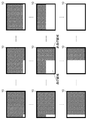
- FIG. 7A is a schematic diagram for explaining a difference in light emission luminance caused by a change in driving load.
- FIG. 7B is a schematic diagram for explaining a difference in light emission luminance caused by a change in driving load.
- FIG. 8A is a schematic diagram for explaining another example of a difference in light emission luminance caused by a change in driving load.
- FIG. 8B is a schematic diagram for explaining another example of a difference in light emission luminance caused by a change in driving load.
- FIG. 9 is a diagram schematically showing measurement of light emission luminance performed for setting the correction coefficient in the first embodiment of the present invention.
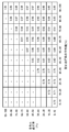
- FIG. 10 is a diagram showing an example of the correction coefficient in the first embodiment of the present invention.
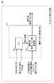
- FIG. 11 is a circuit block diagram of the sustain pulse number correction unit in the first embodiment of the present invention.
- FIG. 12 is a diagram showing a part of a circuit block of the timing generation circuit according to the second embodiment of the present invention.
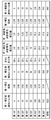
- FIG. 13 is a diagram for explaining “second correction” in the second embodiment of the present invention using specific numerical values.
- FIG. 14 is a diagram showing a part of a circuit block of the timing generation circuit according to the third embodiment of the present invention.
- FIG. 15 is a diagram for describing “third correction” in the third embodiment of the present invention using specific numerical values.
- FIG. 16 is a circuit block diagram of the plasma display device in accordance with the fourth exemplary embodiment of the present invention.
- FIG. 12 is a diagram showing a part of a circuit block of the timing generation circuit according to the second embodiment of the present invention.
- FIG. 13 is a diagram for explaining “second correction” in the second embodiment of the present invention using specific numerical values.
- FIG. 14 is a diagram showing a part of
- FIG. 17 is a diagram showing a part of a circuit block of the timing generation circuit according to the fourth embodiment of the present invention.
- FIG. 18 is a diagram illustrating an example of setting a variable k in the fourth embodiment of the present invention.
- FIG. 19 is a characteristic diagram showing the relationship between the all-cell lighting rate and the sustaining current in the plasma display device.
- FIG. 20 is a diagram showing a part of a circuit block of the timing generation circuit according to the fifth embodiment of the present invention.
- FIG. 21 is a diagram for explaining an example of “third correction” performed with higher accuracy in the fifth embodiment of the present invention, using specific numerical values.
- FIG. 1 is an exploded perspective view showing the structure of panel 10 in accordance with the first exemplary embodiment of the present invention.
- a plurality of display electrode pairs 24 each including a scanning electrode 22 and a sustaining electrode 23 are formed on a glass front substrate 21.
- a dielectric layer 25 is formed so as to cover the scan electrode 22 and the sustain electrode 23, and a protective layer 26 is formed on the dielectric layer 25.
- the protective layer 26 is made of a material mainly composed of magnesium oxide (MgO).
- a plurality of data electrodes 32 are formed on the rear substrate 31, a dielectric layer 33 is formed so as to cover the data electrodes 32, and a grid-like partition wall 34 is formed thereon.
- a phosphor layer 35 that emits light of each color of red (R), green (G), and blue (B) is provided on the side surface of the partition wall 34 and on the dielectric layer 33.
- the front substrate 21 and the rear substrate 31 are arranged to face each other so that the display electrode pair 24 and the data electrode 32 intersect with each other with a minute discharge space interposed therebetween.
- the outer peripheral part is sealed with sealing materials, such as glass frit.
- a mixed gas of neon and xenon is sealed in the discharge space inside as a discharge gas.
- a discharge gas having a xenon partial pressure of about 10% is used to improve luminous efficiency.
- the discharge space is partitioned into a plurality of sections by partition walls 34, and discharge cells are formed at the intersections between the display electrode pairs 24 and the data electrodes 32.
- a color image is displayed on the panel 10 by discharging and emitting (lighting) these discharge cells.
- R red
- G green
- B blue discharge cells
- the structure of the panel 10 is not limited to the above-described structure, and may be, for example, provided with a stripe-shaped partition wall.
- the mixing ratio of the discharge gas is not limited to the above-described numerical values, and may be other mixing ratios.
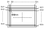
- FIG. 2 is an electrode array diagram of panel 10 in accordance with the first exemplary embodiment of the present invention.
- the panel 10 includes n scan electrodes SC1 to SCn (scan electrodes 22 in FIG. 1) and n sustain electrodes SU1 to SUn (sustain electrodes 23 in FIG. 1) that are long in the row direction.
- M data electrodes D1 to Dm (data electrodes 32 in FIG. 1) that are long in the column direction are arranged.
- m ⁇ n discharge cells are formed in the discharge space, and a region where m ⁇ n discharge cells are formed becomes an image display surface of the panel 10.
- the plasma display device in this embodiment performs gradation display by a subfield method.
- the subfield method one field is divided into a plurality of subfields on the time axis, and a luminance weight is set for each subfield.
- An image is displayed on the panel 10 by controlling light emission / non-light emission of each discharge cell for each subfield.
- the luminance weight represents a ratio of the luminance magnitudes displayed in each subfield, and the number of sustain pulses corresponding to the luminance weight is generated in the sustain period in each subfield.
- the subfield of luminance weight “8” sustain pulses that are eight times as many as the subfield of luminance weight “1” are generated in the sustain period, and the number of sustain pulses is four times that of the subfield of luminance weight “2”.
- a pulse is generated during the sustain period. Therefore, the subfield with the luminance weight “8” emits light with a luminance about eight times that of the subfield with the luminance weight “1”, and emits light with about four times the luminance of the subfield with the luminance weight “2”. Therefore, various gradations can be displayed and images can be displayed by selectively causing each subfield to emit light in a combination according to the image signal.
- one field is composed of eight subfields (first SF, second SF,..., Eighth SF), and each subfield is set so that the luminance weight becomes larger in the later subfield.
- each subfield is set so that the luminance weight becomes larger in the later subfield.
- the R signal, the G signal, and the B signal can be displayed with 256 gradations from 0 to 255, respectively.
- an initializing operation is performed in all the cells to generate an initializing discharge in the initializing period of one subfield, and an immediately preceding period is set in the initializing period of the other subfield.
- a selective initializing operation for selectively generating an initializing discharge is performed on a discharge cell that has generated a sustaining discharge in the sustain period of the subfield.
- the all-cell initialization operation is performed in the initialization period of the first SF and the selective initialization operation is performed in the initialization period of the second SF to the eighth SF.
- the light emission not related to the image display is only the light emission due to the discharge of the all-cell initializing operation in the first SF. Therefore, the black luminance, which is the luminance of the black display region where no sustain discharge occurs, is only weak light emission in the all-cell initialization operation, and an image with high contrast can be displayed on the panel 10.
- the number of sustain pulses obtained by multiplying the luminance weight of each subfield by a predetermined proportional constant is applied to each display electrode pair 24.
- This proportionality constant is the luminance magnification.
- the luminance magnification when the luminance magnification is 1, four sustain pulses are generated in the sustain period of the subfield having the luminance weight “2”, and the scan electrode 22 and the sustain electrode 23 are maintained twice. A pulse is to be applied.
- the number of sustain pulses obtained by multiplying the luminance weight of each subfield by a predetermined luminance magnification is applied to each of scan electrode 22 and sustain electrode 23. Therefore, when the luminance magnification is 2 times, the number of sustain pulses generated in the sustain period of the subfield of luminance weight “2” is 8, and when the luminance magnification is 3, the subfield of luminance weight “2” is maintained.
- the number of sustain pulses generated in the period is 12.
- the number of subfields constituting one field and the luminance weight of each subfield are not limited to the above values.
- the structure which switches a subfield structure based on an image signal etc. may be sufficient.
- the lighting rate for each subfield detected by the all-cell lighting rate detection circuit 46 and the partial lighting rate detection circuit 47 described later ratio of the number of discharge cells to be lit to the predetermined number of discharge cells.
- the number of sustain pulses generated is changed according to the above. Thereby, the linearity of the gradation in the display image of the panel 10 is maintained, and the image display quality is improved.
- the outline of the drive voltage waveform and the configuration of the drive circuit will be described first, and then the configuration for controlling the number of sustain pulses generated according to the lighting rate will be described.
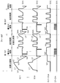
- FIG. 3 is a waveform diagram of driving voltage applied to each electrode of panel 10 in the first exemplary embodiment of the present invention.
- scan electrode SC1 that performs the address operation first in the address period
- scan electrode SCn that performs the address operation last in the address period
- sustain electrode SU1 to sustain electrode SUn and data electrode D1 to data electrode Dm are applied.
- a drive voltage waveform is shown.
- FIG. 3 shows driving voltage waveforms of two subfields.
- the two subfields are a first subfield (first SF) that is an all-cell initializing subfield and a second subfield (second SF) that is a selective initializing subfield.
- the drive voltage waveform in the other subfields is substantially the same as the drive voltage waveform of the second SF except that the number of sustain pulses generated in the sustain period is different.
- scan electrode SCi, sustain electrode SUi, and data electrode Dk in the following represent electrodes selected from the electrodes based on image data (data indicating lighting / non-lighting for each subfield).
- the first SF which is an all-cell initialization subfield, will be described.
- 0 (V) is applied to each of the data electrode D1 to the data electrode Dm and the sustain electrode SU1 to the sustain electrode SUn.
- Voltage Vi1 is applied to scan electrode SC1 through scan electrode SCn.
- Voltage Vi1 is set to a voltage lower than the discharge start voltage with respect to sustain electrode SU1 through sustain electrode SUn.
- a ramp waveform voltage that gently rises from voltage Vi1 to voltage Vi2 is applied to scan electrode SC1 through scan electrode SCn.
- this ramp waveform voltage is referred to as “up-ramp voltage L1”.
- Voltage Vi2 is set to a voltage exceeding the discharge start voltage with respect to sustain electrode SU1 through sustain electrode SUn.
- An example of the gradient of the up-ramp voltage L1 is a numerical value of about 1.3 V / ⁇ sec.
- the wall voltage on the electrode represents a voltage generated by wall charges accumulated on the dielectric layer covering the electrode, the protective layer, the phosphor layer, and the like.
- a scan pulse of voltage Va is sequentially applied to scan electrode SC1 through scan electrode SCn.
- an address pulse of positive voltage Vd is applied to data electrode Dk corresponding to the discharge cell to emit light.
- voltage Ve2 is applied to sustain electrode SU1 through sustain electrode SUn
- voltage Vc is applied to scan electrode SC1 through scan electrode SCn.
- a scan pulse of negative voltage Va is applied to scan electrode SC1 in the first row, and positive voltage Vd is applied to data electrode Dk of the discharge cell that should emit light in the first row of data electrodes D1 to Dm. Apply the write pulse.
- the voltage difference at the intersection between the data electrode Dk and the scan electrode SC1 is the difference between the wall voltage on the data electrode Dk and the wall voltage on the scan electrode SC1 due to the difference between the externally applied voltages (voltage Vd ⁇ voltage Va). It will be added.
- the voltage difference between data electrode Dk and scan electrode SC1 exceeds the discharge start voltage, and a discharge is generated between data electrode Dk and scan electrode SC1.
- the voltage difference between sustain electrode SU1 and scan electrode SC1 is the difference between the externally applied voltages (voltage Ve2 ⁇ voltage Va) and sustain electrode SU1.
- the difference between the upper wall voltage and the wall voltage on the scan electrode SC1 is added.
- the sustain electrode SU1 and the scan electrode SC1 are not easily discharged but are likely to be discharged. Can do.
- a discharge generated between the data electrode Dk and the scan electrode SC1 can be triggered to generate a discharge between the sustain electrode SU1 and the scan electrode SC1 in the region intersecting the data electrode Dk.
- an address discharge is generated in the discharge cell to emit light, a positive wall voltage is accumulated on scan electrode SC1, a negative wall voltage is accumulated on sustain electrode SU1, and a negative wall voltage is also accumulated on data electrode Dk. Is accumulated.
- an address operation is performed in which an address discharge is generated in the discharge cells that should emit light in the first row and a wall voltage is accumulated on each electrode.
- the voltage at the intersection between the data electrode 32 and the scan electrode SC1 to which the address pulse is not applied does not exceed the discharge start voltage, so the address discharge does not occur.
- the address operation described above is performed until the discharge cell in the n-th row, and the address period ends.
- sustain pulses of the number obtained by multiplying the luminance weight by a predetermined luminance magnification are alternately applied to the display electrode pair 24 to generate a sustain discharge in the discharge cell that has generated the address discharge, and the discharge cell emits light.
- a sustain pulse of positive voltage Vs is applied to scan electrode SC1 through scan electrode SCn, and a ground potential serving as a base potential, that is, 0 (V) is applied to sustain electrode SU1 through sustain electrode SUn.
- the voltage difference between scan electrode SCi and sustain electrode SUi is the difference between the wall voltage on scan electrode SCi and the wall voltage on sustain electrode SUi added to sustain pulse voltage Vs. It will be a thing.
- the voltage difference between scan electrode SCi and sustain electrode SUi exceeds the discharge start voltage, and a sustain discharge occurs between scan electrode SCi and sustain electrode SUi. Then, the phosphor layer 35 emits light by the ultraviolet rays generated by this discharge. Further, due to this discharge, a negative wall voltage is accumulated on scan electrode SCi, and a positive wall voltage is accumulated on sustain electrode SUi. Furthermore, a positive wall voltage is also accumulated on the data electrode Dk. In the discharge cells in which no address discharge has occurred in the address period, no sustain discharge occurs, and the wall voltage at the end of the initialization period is maintained.
- 0 (V) as a base potential is applied to scan electrode SC1 through scan electrode SCn, and a sustain pulse is applied to sustain electrode SU1 through sustain electrode SUn.
- the voltage difference between the sustain electrode SUi and the scan electrode SCi exceeds the discharge start voltage.
- a sustain discharge is generated again between sustain electrode SUi and scan electrode SCi, a negative wall voltage is accumulated on sustain electrode SUi, and a positive wall voltage is accumulated on scan electrode SCi.
- the number of sustain pulses obtained by multiplying the luminance weight by the luminance magnification is alternately applied to scan electrode SC1 through scan electrode SCn and sustain electrode SU1 through sustain electrode SUn. By doing so, sustain discharge is continuously generated in the discharge cells that have generated address discharge in the address period.
- 0 (V) is applied to scan electrode SC1 to scan electrode SCn while 0 (V) is applied to sustain electrode SU1 to sustain electrode SUn and data electrode D1 to data electrode Dm.
- 0 (V) is applied to scan electrode SC1 to scan electrode SCn while 0 (V) is applied to sustain electrode SU1 to sustain electrode SUn and data electrode D1 to data electrode Dm.
- this ramp waveform voltage is referred to as “erasing ramp voltage L3”.
- the erasing ramp voltage L3 is set to a steeper slope than the rising ramp voltage L1.
- a numerical value of about 10 V / ⁇ sec can be cited.
- the charged particles generated by the weak discharge are accumulated on the sustain electrode SUi and the scan electrode SCi so as to alleviate the voltage difference between the sustain electrode SUi and the scan electrode SCi. Therefore, in the discharge cell in which the sustain discharge has occurred, part or all of the wall voltage on scan electrode SCi and sustain electrode SUi is erased while leaving the positive wall voltage on data electrode Dk. That is, the discharge generated by the erasing ramp voltage L3 functions as an “erasing discharge” for erasing unnecessary wall charges accumulated in the discharge cell in which the sustain discharge has occurred.
- a drive voltage waveform in which the first half of the initialization period in the first SF is omitted is applied to each electrode.
- Voltage Ve1 is applied to sustain electrode SU1 through sustain electrode SUn, and 0 (V) is applied to data electrode D1 through data electrode Dm.
- Scan electrode SC1 through scan electrode SCn are applied with down-ramp voltage L4 that gently falls from voltage Vi3 ′ (eg, 0 (V)) that is less than the discharge start voltage toward negative voltage Vi4 that exceeds the discharge start voltage. .
- voltage Vi3 ′ eg, 0 (V)
- a numerical value of about ⁇ 2.5 V / ⁇ sec can be given.
- the initializing operation in the second SF is a selective initializing operation in which initializing discharge is generated for the discharge cells that have generated sustain discharge in the sustain period of the immediately preceding subfield.
- a drive voltage waveform similar to that in the first SF address period and sustain period is applied to each electrode.
- the same drive voltage waveform as that of the second SF is applied to each electrode except for the number of sustain pulses.
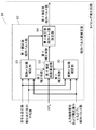
- FIG. 4 is a circuit block diagram of plasma display device 1 according to the first exemplary embodiment of the present invention.
- the plasma display apparatus 1 includes a panel 10, an image signal processing circuit 41, a data electrode driving circuit 42, a scanning electrode driving circuit 43, a sustain electrode driving circuit 44, a timing generation circuit 45, an all-cell lighting rate detection circuit 46, and a partial lighting rate detection.
- the circuit 47 and a power supply circuit (not shown) for supplying necessary power to each circuit block are provided.
- the image signal processing circuit 41 assigns a gradation value to each discharge cell based on the input image signal sig. Then, the gradation value is converted into image data indicating light emission / non-light emission for each subfield.
- each gradation value of R, G, and B is assigned to each discharge cell based on the R signal, the G signal, and the B signal.
- the input image signal sig includes a luminance signal (Y signal) and a saturation signal (C signal, RY signal and BY signal, or u signal and v signal)
- the luminance signal and Based on the saturation signal, R signal, G signal, and B signal are calculated, and then R, G, and B gradation values (gradation values expressed in one field) are assigned to each discharge cell.
- the R, G, and B gradation values assigned to each discharge cell are converted into image data indicating light emission / non-light emission for each subfield.
- the all-cell lighting rate detection circuit 46 sets the ratio of the number of discharge cells to be lit to the number of all discharge cells on the image display surface of the panel 10 as “all-cell lighting rate” based on the image data for each subfield. Detect for each field. Then, a signal indicating the detected all-cell lighting rate is output to the timing generation circuit 45.
- the partial lighting rate detection circuit 47 divides the image display surface of the panel 10 into a plurality of regions, and discharges to be lit with respect to the number of discharge cells in each region for each region and each subfield based on the image data for each subfield. The ratio of the number of cells is detected as “partial lighting rate”.
- the partial lighting rate detection circuit 47 includes, for example, a region composed of a plurality of scan electrodes 22 connected to one of ICs that drive the scan electrodes 22 (hereinafter referred to as “scan ICs”). Although the configuration may be such that the partial lighting rate is detected as a region, in this embodiment, the partial lighting rate is detected by regarding one pair of display electrodes 24 as one region.
- the partial lighting rate detection circuit 47 has an average value detection circuit 48.
- Average value detection circuit 48 compares the partial lighting rate detected by partial lighting rate detection circuit 47 with a predetermined threshold value (hereinafter referred to as “partial lighting rate threshold value”). And the average value of the partial lighting rate in the display electrode pair 24 excluding the display electrode pair 24 in which the partial lighting rate is equal to or lower than the partial lighting rate threshold value, that is, the display electrode pair 24 in which the partial lighting rate exceeds the partial lighting rate threshold value. Is calculated for each subfield, and a signal representing the result is output to the timing generation circuit 45.
- the average value of the partial lighting rates is calculated for 880 pairs of display electrodes 24 whose partial lighting rate is larger than the partial lighting rate threshold.
- the partial lighting rate threshold is set to “0%”. This is because the display electrode pair 24 in which the discharge cells to be lit are not substantially generated is excluded when calculating the average value of the partial lighting rates.
- the partial lighting rate threshold value is not limited to the above-described numerical values.
- the partial lighting rate threshold value is desirably set to an optimum value based on the characteristics of the panel 10 and the specifications of the plasma display device 1.
- a normalization operation for percentage display is performed when calculating the total cell lighting rate and the partial lighting rate.
- the calculated number of discharge cells to be lit may be used as the total cell lighting rate and the partial lighting rate.
- the discharge cells that are lit are also referred to as “lighted cells”, and the discharge cells that are not lit are also referred to as “non-lighted cells”.
- the timing generation circuit 45 generates various timing signals for controlling the operation of each circuit block based on outputs from the horizontal synchronization signal H, the vertical synchronization signal V, the all-cell lighting rate detection circuit 46, and the partial lighting rate detection circuit 47. To do. Then, the generated timing signal is supplied to each circuit block (image signal processing circuit 41, data electrode drive circuit 42, scan electrode drive circuit 43, sustain electrode drive circuit 44, etc.).
- the number of generated sustain pulses is changed according to the average value of the all-cell lighting rate and the partial lighting rate.
- the number of sustain pulses set in the timing generation circuit 45 based on the input image signal and the luminance weight set for each subfield is expressed by a correction coefficient based on the average value of the all-cell lighting rate and the partial lighting rate.
- the timing generation circuit 45 has a sustain pulse number correction unit (not shown) that can correct the number of sustain pulses generated based on the average value of the all-cell lighting rate and the partial lighting rate.
- a plurality of different correction coefficients are stored in advance in the sustain pulse number correction unit in association with the all-cell lighting rate and the partial lighting rate, and any one of them is stored in the all-cell lighting rate and the partial lighting rate. It is assumed that a lookup table that can be read out according to the average value of the rate is provided. Details of these configurations will be described later. However, the present invention is not limited to this configuration, and may have any configuration as long as the same operation is performed.
- Scan electrode drive circuit 43 has an initialization waveform generation circuit (not shown), sustain pulse generation circuit 50, and scan pulse generation circuit (not shown).
- the initialization waveform generating circuit generates an initialization waveform to be applied to scan electrode SC1 through scan electrode SCn during the initialization period.
- Sustain pulse generation circuit 50 generates a sustain pulse to be applied to scan electrode SC1 through scan electrode SCn during the sustain period.
- the scan pulse generating circuit includes a plurality of scan electrode driving ICs (scan ICs), and generates scan pulses to be applied to scan electrode SC1 through scan electrode SCn in the address period.
- Scan electrode driving circuit 43 drives scan electrode SC1 through scan electrode SCn based on the timing signal supplied from timing generation circuit 45, respectively.
- the data electrode drive circuit 42 converts the data for each subfield constituting the image data into signals corresponding to the data electrodes D1 to Dm. Then, based on the signal and the timing signal supplied from the timing generation circuit 45, the data electrodes D1 to Dm are driven.
- Sustain electrode drive circuit 44 includes sustain pulse generation circuit 80 and a circuit for generating voltage Ve1 and voltage Ve2 (not shown). Based on a timing signal supplied from timing generation circuit 45, sustain electrode SU1 to sustain electrode SUn are provided. Drive.
- the operation for turning on the switching element is expressed as “on”
- the operation for shutting off is expressed as “off”
- the signal for turning on the switching element is expressed as “Hi”
- the signal for turning off is expressed as “Lo”.
- FIG. 5 is a circuit diagram showing a configuration of scan electrode driving circuit 43 of plasma display device 1 in accordance with the first exemplary embodiment of the present invention.
- Scan electrode drive circuit 43 includes sustain pulse generation circuit 50 on the scan electrode 22 side, initialization waveform generation circuit 53, and scan pulse generation circuit 54.
- Each output terminal of scan pulse generating circuit 54 is connected to each of scan electrode SC1 to scan electrode SCn of panel 10. This is so that the scan pulse can be individually applied to each of the scan electrodes 22 in the address period.
- the initialization waveform generation circuit 53 raises or lowers the reference potential A of the scan pulse generation circuit 54 in a ramp shape during the initialization period, and generates the initialization waveform shown in FIG.
- the reference potential A is a voltage input to the scan pulse generation circuit 54 as shown in FIG.
- the sustain pulse generation circuit 50 includes a power recovery circuit 51 and a clamp circuit 52.
- the power recovery circuit 51 has a power recovery capacitor C10, a switching element Q11, a switching element Q12, a backflow prevention diode D11, a backflow prevention diode D12, and a resonance inductor L10. Then, the interelectrode capacitance Cp and the inductor L10 are LC-resonated to cause the sustain pulse to rise and fall.
- Clamp circuit 52 includes switching element Q13 for clamping scan electrode SC1 through scan electrode SCn to voltage Vs, and switching element Q14 for clamping scan electrode SC1 through scan electrode SCn to the base potential of 0 (V). is doing. Then, scan electrode SC1 through scan electrode SCn are connected to power supply VS via switching element Q13, and scan electrode SC1 through scan electrode SCn are clamped to voltage Vs. Scan electrode SC1 through scan electrode SCn are connected to the ground potential via switching element Q14, and scan electrode SC1 through scan electrode SCn are clamped to 0 (V).
- Sustain pulse generation circuit 50 is connected to power recovery circuit 51 by clamping switching element Q11, switching element Q12, switching element Q13, and switching element Q14 in accordance with the timing signal output from timing generation circuit 45.
- the circuit 52 is operated to generate a sustain pulse.
- the switching element Q11 when the sustain pulse is raised, the switching element Q11 is turned on to resonate the interelectrode capacitance Cp and the inductor L10, and from the power recovery capacitor C10, the scanning electrode passes through the switching element Q11, the diode D11, and the inductor L10. Power is supplied to SC1 through scan electrode SCn.
- switching element Q13 When the voltage of scan electrode SC1 through scan electrode SCn approaches voltage Vs, switching element Q13 is turned on, and the circuit for driving scan electrode SC1 through scan electrode SCn is switched from power recovery circuit 51 to clamp circuit 52. Scan electrode SC1 through scan electrode SCn are clamped to voltage Vs.
- the switching element Q12 is turned on to resonate the interelectrode capacitance Cp and the inductor L10, and the interelectrode capacitance Cp is used for power recovery through the inductor L10, the diode D12, and the switching element Q12.
- the power is recovered in the capacitor C10.
- switching element Q14 is turned on, and a circuit for driving scan electrode SC1 through scan electrode SCn is connected from power recovery circuit 51 to clamp circuit 52. And the scan electrodes SC1 to SCn are clamped to 0 (V) which is the base potential.
- switching elements can be configured using generally known elements such as MOSFETs and IGBTs.
- Scan pulse generation circuit 54 includes a switch 72 for connecting reference potential A to negative voltage Va in the write period, a power supply VC used for generating voltage Vc, and n scan electrodes SC1 to SCn.
- Switching elements QH1 to QHn and switching elements QL1 to QLn for applying a scan pulse to each of them are provided.
- Switching elements QH1 to QHn and switching elements QL1 to QLn are integrated into a plurality of ICs for each of a plurality of outputs. This IC is a scanning IC. Then, by turning off the switching element QHi and turning on the switching element QLi, a scan pulse of the negative voltage Va is applied to the scan electrode SCi via the switching element QLi.
- the switching elements QL1 to QLn are turned on by turning off the switching elements QH1 to QHn and turning on the switching elements QL1 to QLn.
- An initialization waveform or a sustain pulse is applied to each of scan electrode SC1 through scan electrode SCn via switching element QLn.
- FIG. 6 is a circuit diagram showing a configuration of sustain electrode drive circuit 44 of plasma display device 1 in accordance with the first exemplary embodiment of the present invention.
- the interelectrode capacitance of the panel 10 is shown as Cp, and the circuit diagram of the scan electrode driving circuit 43 is omitted.
- Sustain electrode drive circuit 44 includes sustain pulse generation circuit 80 having a configuration substantially similar to sustain pulse generation circuit 50.
- Sustain pulse generation circuit 80 includes power recovery circuit 81 and clamp circuit 82, and is connected to sustain electrode SU1 through sustain electrode SUn of panel 10.
- the output voltage of the sustain electrode drive circuit 44 is applied in parallel to all the sustain electrodes 23, and the sustain electrode drive circuit 44 drives all the sustain electrodes 23 at once. This is because, in both the writing period and the sustain period, it is not necessary to individually drive the sustain electrodes 23 unlike the scan electrodes 22, and it is sufficient to apply the drive voltage to all the sustain electrodes 23 at the same time.
- the power recovery circuit 81 includes a power recovery capacitor C20, a switching element Q21, a switching element Q22, a backflow prevention diode D21, a backflow prevention diode D22, and a resonance inductor L20.
- Clamp circuit 82 has switching element Q23 for clamping sustain electrode SU1 through sustain electrode SUn to voltage Vs, and switching element Q24 for clamping sustain electrode SU1 through sustain electrode SUn to the ground potential (0 (V)). is doing.
- Sustain pulse generation circuit 80 generates a sustain pulse by switching on and off each switching element according to a timing signal output from timing generation circuit 45.
- the operation of sustain pulse generating circuit 80 is the same as that of sustain pulse generating circuit 50 described above, and a description thereof will be omitted.
- sustain electrode drive circuit 44 includes power source VE1 that generates voltage Ve1, switching element Q26 for applying voltage Ve1 to sustain electrode SU1 through sustain electrode SUn, switching element Q27, and power source ⁇ VE that generates voltage ⁇ Ve.
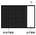
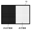
- FIGS. 7A and 7B are schematic diagrams for explaining a difference in light emission luminance caused by a change in driving load.
- FIGS. 7A and 7B are schematic views showing a light emission state of the image display surface of the panel 10 in a certain subfield. It is shown in. Moreover, the black area
- FIG. 7A is a diagram schematically showing the light emission state of the panel 10 when the lighting area is set to 80% of the image display surface, and FIG. 7B is when the lighting area is set to 20% of the image display surface.
- the display electrode pairs 24 are arranged so as to extend in the row direction (direction parallel to the long side of the panel 10, or the horizontal direction in the drawing) in the same manner as the panel 10 shown in FIG. Shall.
- the display electrode pairs 24 are arranged extending in the row direction, the number of lighting cells generated on the display electrode pair 24 when the panel 10 is caused to emit light by changing the lighting region as shown in FIGS. 7A and 7B. Changes. As the lighting region becomes narrower, the number of lighting cells generated on the display electrode pair 24 decreases. Therefore, for example, the display electrode pair in the light emitting state shown in FIG. 7B (when the area of the lighting region is small) is more than the display electrode pair 24 in the light emitting state shown in FIG. 7A (when the area of the lighting region is large). 24 has a smaller driving load. Therefore, the display electrode pair 24 in the light emission state shown in FIG.
- the 7B has a lower voltage drop of the drive voltage (for example, the sustain pulse) than the display electrode pair 24 in the light emission state shown in FIG. 7A. That is, it is considered that the discharge intensity is stronger in the sustain discharge in the lighting region shown in FIG. 7B than in the sustain discharge in the lighting region shown in FIG. 7A. As a result, it is considered that the light emission luminance is higher in the lighting region shown in FIG. 7B than in the lighting region shown in FIG. 7A.
- the drive voltage for example, the sustain pulse
- FIGS. 8A and 8B are schematic diagrams for explaining another example of a difference in light emission luminance caused by a change in driving load
- FIGS. 8A and 8B show light emission on the image display surface of the panel 10 in a certain subfield.
- the state is schematically shown.
- FIG. 8A is a diagram schematically showing the light emission state of the panel 10 when the lighting region is set to 50% of the image display surface
- FIG. 8B is a diagram when the lighting region is set to 25% of the image display surface. It is the figure which showed the light emission state of the panel 10 of this.
- FIGS. 7A and 7B show an example in which the partial lighting rate changes and the driving load of the display electrode pair 24 in the lighting region changes.
- the partial lighting rate in the lighting region does not change, even if the total number of lighting cells, that is, the total cell lighting rate changes, the light emission luminance in the lighting region changes.
- the sustain electrode drive circuit 44 since the sustain electrode drive circuit 44 is connected in parallel to all the sustain electrodes 23 and all the sustain electrodes 23 are collectively driven by the sustain electrode drive circuit 44, the all-cell lighting rate is It is considered that the main reason is that the voltage drop generated in the output voltage from the sustain electrode drive circuit 44 changes due to the change in.
- the total cell lighting rate and the partial lighting rate are detected for each subfield.
- the average value of the partial lighting rates is detected. That is, in this embodiment, the total cell lighting rate and the average value of the partial lighting rates are detected for each subfield.
- the number of sustain pulses generated in the sustain period of the subfield in which the detection is performed is changed, and the luminance generated in the sustain period is controlled.
- This luminance is a luminance obtained by accumulating light emission generated by the sustain discharge in the sustain period.
- the luminance of each subfield is kept at a predetermined brightness. Thereby, the linearity of the gradation in the display image can be maintained and the image display quality can be improved.
- the number of sustain pulses that are set based on the input image signal and the luminance weight is corrected with a correction coefficient that is set based on the average value of all-cell lighting rates and partial lighting rates. .
- a correction coefficient that is set based on the average value of all-cell lighting rates and partial lighting rates.
- FIG. 9 is a diagram schematically showing the measurement of the light emission luminance performed for setting the correction coefficient in the first embodiment of the present invention.
- an image in which a lighting area and a non-lighting area are divided into two is displayed on the panel 10. Then, while measuring the light emission luminance in the lighting region, the area of the lighting region is gradually changed as shown in FIG.
- the lighting area is 10% in each of the row direction (horizontal direction in the drawing) and the column direction (direction parallel to the short side of the panel 10 and vertical direction in the drawing) of the image display surface of the panel 10.
- the image set to is displayed, and the light emission luminance of the lighting area is measured.
- each emission brightness is normalized by setting the reference emission brightness to “1”.
- the emission luminance of an image in which the average values of the all-cell lighting rate and the partial lighting rate are both 100% is set as the reference emission luminance, and each emission luminance is normalized.
- the reciprocal of the numerical value is calculated, respectively.
- the calculation result is used as a correction coefficient. For example, when the light emission luminance of an image in which the average values of the all-cell lighting rate and the partial lighting rate are both 100% is “1”, the image in which the all-cell lighting rate is 5% and the average value of the partial lighting rate is 40%. If the light emission brightness of “1.25” is “1.25”, the correction coefficient when “0.80”, which is the reciprocal of “1.25”, is 5% for the total cell lighting rate and the average value of the partial lighting rate is 40%. And
- FIG. 10 is a diagram showing an example of the correction coefficient in the first embodiment of the present invention.
- FIG. 11 is a circuit block diagram of sustain pulse number correction unit 61 in the first embodiment of the present invention.
- the timing generation circuit 45 in the present embodiment has a sustain pulse number correction unit 61.
- the sustain pulse number correcting unit 61 includes a lookup table 62 (indicated as “LUT” in the drawing) and a post-correction sustain pulse number setting unit 63.
- the look-up table 62 stores a plurality of correction coefficients, and any one correction coefficient can be read based on the average value of the all-cell lighting rate and the partial lighting rate.
- the post-correction sustain pulse number setting unit 63 corrects the number of sustain pulses generated based on the input image signal and the luminance weight (hereinafter also simply referred to as “sustain pulse number”) read from the lookup table 62. Multiply by coefficient and output. The multiplication result is the number of sustain pulses after correction (number of sustain pulses after correction).
- timing generation circuit 45 in each subfield, the number of sustain pulses equal to the number of sustain pulses after correction output from sustain pulse number setting unit 63 after correction is generated from sustain pulse generation circuit 50 and sustain pulse generation circuit 80.
- a timing signal for controlling each circuit block is generated so as to be output.
- the total cell lighting rate (from 0% to 100%) is divided into 10 steps every 10%, and the average value of the partial lighting rate (from 0% to 100%) for each of the total cell lighting rates is shown.
- the correction coefficient corresponding to the average value of each of the all-cell lighting rate and the partial lighting rate is shown by dividing into 10 stages of every 10%. For example, when the total cell lighting rate is 100%, the average value of the partial lighting rates is never less than 100%. Such a combination that does not substantially occur is indicated by “ ⁇ ” in the drawing. Note that FIG. 10 is merely an example, and the present invention is not limited to the partition shown in FIG. 10 at all in terms of the average values of all-cell lighting rates and partial lighting rates.
- the correction coefficient is not limited to the numerical values shown in FIG.
- each correction coefficient obtained by the above-described method is associated with the average value of the all-cell lighting rate and the partial lighting rate and is matrixed, and is stored in the lookup table 62.
- one of the plurality of correction coefficients stored in the lookup table 62 is read out based on the average value of the all-cell lighting rate and the partial lighting rate detected for each subfield. Then, the number of sustain pulses generated in the subfield is corrected using the read correction coefficient.
- the number of sustain pulses set based on the input image signal and luminance weight in the sixth SF is “128”, the total cell lighting rate in the sixth SF is 5%, and the average value of the partial lighting rates is 45%.
- the correction coefficient obtained from the data of the lookup table 62 shown in FIG. 10 is “0.80”
- the post-correction sustain pulse number setting unit 63 multiplies “128” by “0.80”. Since the multiplication result is “102”, the number of sustain pulses generated in the sixth SF is set to “102”. Thereby, the brightness of the sixth SF can be set to 80% when the number of sustain pulses generated is “128”. Therefore, the luminance of the sixth SF can be made equal to the luminance when the all-cell lighting rate of the sixth SF is 100%.
- the number of sustain pulses set based on the input image signal and the luminance weight is corrected by a correction coefficient based on the average value of the all-cell lighting rate and the partial lighting rate.
- the luminance of each subfield can always be made equal to a predetermined luminance (for example, the luminance when the all-cell lighting rate is 100%) regardless of the lighting state of the discharge cells.
- the average value of all-cell lighting rate and partial lighting rate is detected for each subfield. Then, from the lookup table 62 in which a plurality of preset correction coefficients are stored in association with the average values of all-cell lighting rates and partial lighting rates, the average values of all-cell lighting rates and partial lighting rates detected for each subfield are obtained. First, any one correction coefficient is read out. Then, the post-correction sustain pulse number setting unit 63 corrects the number of sustain pulses generated based on the input image signal and the luminance weight with the correction coefficient.
- the luminance of each subfield is always set to a predetermined luminance (for example, 100% lighting rate of all cells). Brightness), it is possible to maintain the linearity of the gradation in the display image and improve the image display quality.
- each correction coefficient is set by setting the maximum value of the correction coefficient to “1”
- the number of sustain pulses after correction is equal to or decreased from the number of sustain pulses before correction. This shows an example effective when the total time required for each subfield reaches approximately one field and it is difficult to further extend the sustain period to increase the number of sustain pulses.
- the present invention is not limited to this configuration.
- the maximum value of the correction coefficient May be set to be larger than “1” and each correction coefficient may be set so that a subfield in which the number of sustain pulses is generated by the correction is generated.
- the correction shown in the first embodiment is referred to as “first correction”, and the correction coefficient used for “first correction” is “first correction”. It will be called “coefficient”.
- the new correction shown in the present embodiment is called “second correction”, and the correction coefficient used for “second correction” is called “second correction coefficient”. While the “first correction coefficient” is set for each subfield, the “second correction coefficient” is a correction coefficient that is set in common for all subfields in one field.
- FIG. 12 is a diagram showing a part of the circuit block of the timing generation circuit 60 according to the second embodiment of the present invention.
- FIG. 12 shows only circuit blocks related to “first correction” and “second correction”, and other circuit blocks are omitted.
- the timing generation circuit 60 in the present embodiment has a sustain pulse number correction unit 83.
- the sustain pulse number correction unit 83 includes a lookup table 62 (denoted as “LUT” in the drawing), a first post-correction sustain pulse number setting unit 63, a first post-correction sustain pulse number summation unit 68, and a correction. It has a pre-sustain pulse number summation unit 69, a second correction coefficient calculation unit 71, and a second post-correction sustain pulse number setting unit 73.
- the look-up table 62 and the first post-correction sustain pulse number setting unit 63 shown in FIG. 12 have the same configuration and operation as the look-up table 62 and the post-correction sustain pulse number setting unit 63 shown in FIG. The description is omitted.
- the first post-correction sustain pulse number summation unit 68 cumulatively adds the number of sustain pulses after “first correction” in each subfield output from the first post-correction sustain pulse number setting unit 63 over one field period. In this way, the total number of sustain pulses generated in one field period when the “first correction” is performed is calculated.
- the pre-correction sustain pulse number summation unit 69 cumulatively adds the number of sustain pulses of each subfield set based on the input image signal and the luminance weight over one field period. In this way, the total number of sustain pulses generated in one field period when “first correction” is not performed (hereinafter also referred to as “before“ first correction ””) is calculated.
- the second correction coefficient calculation unit 71 divides the numerical value output from the pre-correction sustain pulse number summation unit 69 by the numerical value output from the first post-correction sustain pulse number summation unit 68. That is, the total number of sustain pulses generated in one field period when “first correction” is not performed is divided by the total number of sustain pulses generated in one field period when “first correction” is performed. This calculation result is the “second correction coefficient” in the present embodiment.
- the second post-correction sustain pulse number setting unit 73 multiplies the numerical value output from the first post-correction sustain pulse number setting unit 63 by the “second correction coefficient” output from the second correction coefficient calculation unit 71. That is, the number of sustain pulses after the “first correction” in each subfield is multiplied by the “second correction coefficient” output from the second correction coefficient calculation unit 71. The multiplication result is the “second corrected number of sustain pulses”.
- the second post-correction sustain pulse number setting unit 73 outputs the second post-correction sustain pulse number.
- timing generation circuit 60 in each subfield, the number of sustain pulses equal to the second corrected sustain pulse number output from second corrected sustain pulse number setting unit 73 is equal to sustain pulse generation circuit 50, sustain pulse.
- a timing signal for controlling each circuit block is generated so as to be output from the generation circuit 80.
- FIG. 13 is a diagram for explaining “second correction” in the second embodiment of the present invention using specific numerical values.
- FIG. 13 shows the number of sustain pulses before “first correction”, “first correction coefficient”, the number of sustain pulses after “first correction”, “second correction coefficient”, and “second correction”. The number of subsequent sustain pulses is shown for each subfield.
- the number of sustain pulses generated based on the input image signal and the luminance weight is (4, 8, 16, 32, 64, 128, 256, 512) in each subfield from the first SF to the eighth SF, respectively.
- the total number of sustain pulses in one field period calculated by the number of sustain pulses before correction 69 is “1020”.
- the “first correction coefficient” read from the lookup table 62 based on the average value of the all-cell lighting rate and the partial lighting rate is (1.00, 0.98) in each of the first SF to the eighth SF. , 0.92, 0.90, 0.85, 0.80, 0.74, 0.70).
- the number of sustain pulses after “first correction” of each subfield from the first SF to the eighth SF calculated by the first corrected sustain pulse number setting unit 63 is (4, 8, 15, 29, 54), respectively. , 102, 189, 358) (rounded off after the decimal point).
- the numerical value output from the first post-correction sustain pulse number total unit 68 as the sum of these numerical values is “759”. From these results, the number of sustain pulses generated in one field period after “first correction” is “759”, which is more than “1020” as the number of sustain pulses generated in one field period before “first correction”. 261 "is found to be less.
- the second post-correction sustain pulse number setting unit 73 calculates “1.344” obtained as the “second correction coefficient” from the first SF to the eighth SF calculated by the first post-correction sustain pulse number setting unit 63. (4, 8, 15, 29, 54, 102, 189, 358).
- the number of sustain pulses of each subfield generated after the “second correction” is (5, 11, 20, 39, 73, 137, 254, 481) from the first SF to the eighth SF (decimal point). The following are rounded off). The sum of these values is “1020”. Therefore, the number of sustain pulses generated in one field period can be set to “1020” equal to the total number of sustain pulses before “first correction” by “second correction”.
- the total number of sustain pulses in one field period can be made equal to that before the “first correction”. "I do. With such a configuration, it is possible to maintain the linearity of the gradation in the display image and to prevent the brightness of the display image from being lowered, thereby improving the image display quality.
- the total number of sustain pulses in one field period after “second correction” can be made equal to the total number of sustain pulses in one field period before “first correction”. . Therefore, even when it is difficult to increase the number of sustain pulses by extending the sustain period even if the total time required for each subfield reaches approximately one field, it is stored in the lookup table 62 in the “first correction”. It is possible to make the maximum value of the correction coefficient to be a numerical value larger than “1”. Accordingly, the degree of freedom of the correction coefficient setting range can be increased.
- the configuration in which “second correction” is performed so that the total number of sustain pulses generated in one field period is equal to that before “first correction” has been described.
- the power consumption after the “second correction” may increase more than before the “first correction”. Therefore, in the present embodiment, after the “first correction” shown in the first embodiment, the estimated power consumption in one field period is the power consumption in one field period when the “first correction” is not performed.
- a configuration will be described in which a new correction that is equivalent to the estimated value is further added.
- the new correction shown in the present embodiment is referred to as “third correction”, and the correction coefficient used for “third correction” is “third correction”. This is referred to as “correction coefficient”.
- This “third correction coefficient” is a correction coefficient that is set in common to all subfields in one field.
- FIG. 14 is a diagram showing a part of the circuit block of the timing generation circuit 70 according to the third embodiment of the present invention.
- FIG. 14 shows only circuit blocks related to “first correction” and “third correction”, and omits other circuit blocks.
- the timing generation circuit 70 in the present embodiment has a sustain pulse number correction unit 90.
- the sustain pulse number correcting unit 90 includes a look-up table 62 (denoted as “LUT” in the drawing), a first post-correction sustain pulse number setting unit 63, a multiplying unit 74, a multiplying unit 75, and a sum calculating unit 76. , A total calculation unit 77, a third correction coefficient calculation unit 78, and a third post-correction sustain pulse number setting unit 79.
- the look-up table 62 and the first post-correction sustain pulse number setting unit 63 shown in FIG. 14 have the same configuration and operation as the look-up table 62 and the post-correction sustain pulse number setting unit 63 shown in FIG. The description is omitted.
- Multiplier 74 multiplies the number of sustain pulses of each subfield set based on the input image signal and the luminance weight by the all-cell lighting rate of that subfield. Thereby, the estimated value of the power consumption in each sustain period when the image is displayed without performing the “first correction” is calculated.
- the sum total calculation unit 76 calculates the sum total of one field period of the multiplication result output from the multiplication unit 74. Thereby, the sum total of one field period of the estimated value of the power consumption in each sustain period when the image is displayed without performing the “first correction” is calculated.
- the multiplication unit 75 multiplies the number of sustain pulses after the “first correction” of each subfield output from the first corrected sustain pulse number setting unit 63 by the all-cell lighting rate of the subfield. Thereby, the estimated value of the power consumption in each sustain period when the image is displayed by performing only the “first correction” is calculated.
- the sum total calculation unit 77 calculates the sum total of one field period of the multiplication result output from the multiplication unit 75. As a result, the sum total of one field period of the estimated power consumption in each sustain period when only the “first correction” is displayed is displayed.
- the numerical value calculated in the sum total calculation part 76 and the sum total calculation part 77 represents the estimated value of the power consumption in a maintenance period, this does not represent the power consumption in a strict meaning.
- This estimated value increases the power consumption during the sustain period when the number of sustain pulses is large compared to when the number of sustain pulses is small, and increases when the all-cell lighting rate is high than when the all-cell lighting rate is low. It is only an approximate value obtained using.
- the present invention is not limited to this configuration, and may be configured to use other methods for the power consumption calculation method or the power consumption estimation value calculation method.
- the power consumption that does not contribute to light emission called reactive power by applying a sustain pulse to the scan electrode 22 and the sustain electrode 23 even if the all-cell lighting rate is 0% and no sustain discharge occurs on the image display surface. Occurs. Therefore, an estimated value closer to the actual power consumption is obtained by adding the offset value considering the reactive power to the all-cell lighting rate, and accumulating the result of multiplying the addition result and the number of sustain pulses in one field period. Can be calculated.
- the third correction coefficient calculation unit 78 divides the numerical value output from the total calculation unit 76 by the numerical value output from the total calculation unit 77. That is, the estimated power consumption when the image is displayed without performing the “first correction” is divided by the estimated power consumption when the image is displayed with only the “first correction”. This calculation result is the “third correction coefficient” in the present embodiment.
- the third post-correction sustain pulse number setting unit 79 multiplies the numerical value output from the first post-correction sustain pulse number setting unit 63 by the “third correction coefficient” output from the third correction coefficient calculation unit 78. That is, the number of sustain pulses after the “first correction” in each subfield is multiplied by the “third correction coefficient” output from the third correction coefficient calculation unit 78. This multiplication result is the “number of sustain pulses after the third correction”.
- the third post-correction sustain pulse number setting section 79 outputs the third post-correction sustain pulse number.
- the number of sustain pulses equal to the third corrected sustain pulse number output from the third corrected sustain pulse number setting unit 79 is the sustain pulse generation circuit 50, the sustain pulse.
- a timing signal for controlling each circuit block is generated so as to be output from the generation circuit 80.
- FIG. 15 is a diagram for explaining the “third correction” in the third embodiment of the present invention using specific numerical values.
- FIG. 15 shows the number of sustain pulses before “first correction”, the “first correction coefficient”, the number of sustain pulses after “first correction”, the all-cell lighting rate, and the number before “first correction”.
- the estimated power consumption value, the estimated power consumption value after “first correction”, the “third correction coefficient”, and the number of sustain pulses after “third correction” are shown for each subfield.
- the number of sustain pulses generated based on the input image signal and the luminance weight is (4, 8, 16, 32, 64, 128, 256, 512) in each subfield from the first SF to the eighth SF. .
- the “first correction coefficient” read from the lookup table 62 based on the average value of the all-cell lighting rate and the partial lighting rate is (1.00, 0.98) in each of the first SF to the eighth SF. , 0.92, 0.90, 0.85, 0.80, 0.74, 0.70).
- the number of sustain pulses after “first correction” calculated by the first post-correction sustain pulse number setting unit 63 is (4, 8, 15, 29) in each of the subfields from the first SF to the eighth SF. , 54, 102, 189, 358) (rounded off after the decimal point).
- the lighting rate of all cells in each subfield from the first SF to the eighth SF is (95%, 85%, 35%, 45%, 25%, 15%, 10%, 5%), respectively.
- the numerical value calculated by the multiplication unit 74 as the multiplication value of the number of sustain pulses before the “first correction” and the all-cell lighting rate is (3.8, 3.8, respectively) in each subfield from the first SF to the eighth SF. 6.8, 5.6, 14.4, 16, 19.2, 25.6, 25.6).
- the numerical value output from the total calculation unit 76 as the total of these is “117”. That is, the total power consumption (approximate value) in each sustain period when an image is displayed without performing the “first correction” is “117”.
- the numerical value calculated in the multiplication unit 75 as a multiplication value of the number of sustain pulses after the “first correction” and the all-cell lighting rate is (3.8, each subfield from the first SF to the eighth SF). 6.8, 5.25, 13.05, 13.5, 15.3, 18.9, 17.9).
- the numerical value output from the total calculation unit 77 as the total of these is “94.5”. That is, the total sum (approximate value) of power consumption in each sustain period when only “first correction” is performed to display an image is “94.5”.
- the third post-correction sustain pulse number setting unit 79 obtains “1.238” obtained as the “third correction coefficient” from the first SF to the eighth SF calculated by the first post-correction sustain pulse number setting unit 63. (4, 8, 15, 29, 54, 102, 189, 358).
- the number of sustain pulses of each subfield generated after the “third correction” is (5, 10, 19, 36, 67, 126, 234, 443) from the first SF to the eighth SF (decimal point). The following are rounded off).
- the result of multiplying the number of sustain pulses in each subfield after the “third correction” by the all-cell lighting rate is the first SF to the eighth SF (4.75, 8.5, 6. 65, 16.2, 16.75, 18.9, 23.4, 22.15), and the sum of these is “117.3”. Therefore, the power consumption in one field period can be made equal to the power consumption before the “first correction” by the “third correction”. Further, since the total number of sustain pulses in one field period can be increased as compared with the case where only the “first correction” is performed, it is possible to prevent the brightness of the display image from being lowered and to improve the image display quality. It becomes possible.
- the “third correction” that can make the power consumption in one field period equal to that before the “first correction”. Do. With such a configuration, it is possible to maintain gradation linearity in the display image and prevent the brightness of the display image from decreasing while suppressing an increase in power consumption.
- the estimated value of power consumption in one field period after “third correction” can be made equivalent to that before “first correction”. Therefore, the maximum value of the correction coefficient stored in the lookup table 62 is larger than “1”, and the estimated power consumption value in one field period after “first correction” is larger than that before “first correction”. It can be used for various configurations.
- the “first correction coefficient” is a correction coefficient set in each subfield. Further, as shown in FIG. 10, the “first correction coefficient” increases as the all-cell lighting rate increases, and decreases as the all-cell lighting rate decreases.
- the “first correction coefficient” in each subfield is “1” or less. Therefore, the total number of sustain pulses in one field period after “first correction” is equal to or less than the total number of sustain pulses in one field period before “first correction”. As a result, the “second correction coefficient” is “1” or more.
- the “second correction coefficient” is a correction coefficient that is set in common to all subfields in one field, as described in the second embodiment. Therefore, by performing the “second correction”, the number of sustain pulses is likely to increase more than before the “first correction” in the subfield where the all-cell lighting rate is large (for example, from the first SF to the sixth SF in FIG. 13). In the subfield where the all-cell lighting rate is small, the number of sustain pulses is likely to decrease more easily than before the “first correction” (for example, the seventh SF and the eighth SF in FIG. 13).
- the number of sustain pulses increases in the subfield where the power consumed by one sustain discharge is large (the subfield where the all-cell lighting rate is large) than before the “first correction”. It can be said that the number of sustain pulses is more likely to decrease in the subfield where the power consumed by one sustain discharge is small (the subfield where the all-cell lighting rate is small) than before the “first correction”. As a result, it is considered that the power consumption after the “second correction” may increase more than before the “first correction”.
- the power consumption of the plasma display device 1 is reduced as compared with when the APL is high. Is not a big problem. Rather, it is desirable that an image with a low APL can be displayed brighter in order to improve image display quality.
- the APL is high, the power consumption of the plasma display device 1 is increased. Therefore, the brightness of the display image is prevented from being lowered while suppressing the increase in the power consumption, rather than the “second correction” that increases the power consumption. The “third correction” that can be performed is more desirable.
- the “fourth correction coefficient” is a correction coefficient that is calculated by mixing the “second correction coefficient” and the “third correction coefficient” at a ratio according to the size of the APL, and is all subfields in one field. Is a correction coefficient set in common.
- FIG. 16 is a circuit block diagram of plasma display device 2 in the fourth exemplary embodiment of the present invention.
- the plasma display device 2 includes a panel 10, an image signal processing circuit 41, a data electrode driving circuit 42, a scanning electrode driving circuit 43, a sustain electrode driving circuit 44, a timing generation circuit 91, an all-cell lighting rate detection circuit 46, and a partial lighting rate detection.
- a circuit 47, an APL detection circuit 49, and a power supply circuit (not shown) for supplying power necessary for each circuit block are provided.
- Each circuit block excluding the APL detection circuit 49 and the timing generation circuit 91 has the same configuration and operation as the circuit block of the same name shown in FIG. 4 in the first embodiment.
- the APL detection circuit 49 detects the APL by using a generally known method such as accumulating the luminance value of the input image signal over one field period, and transmits the detected result to the timing generation circuit 91.
- FIG. 17 is a diagram showing a part of the circuit block of the timing generation circuit 91 according to the fourth embodiment of the present invention.
- FIG. 17 shows only circuit blocks related to this embodiment, and other circuit blocks are omitted.
- the timing generation circuit 91 in the present embodiment has a sustain pulse number correction unit 92.
- Sustain pulse number correction unit 92 includes sustain pulse number correction unit 83, sustain pulse number correction unit 90, fourth correction coefficient calculation unit 93, and fourth post-correction sustain pulse number setting unit 94.
- sustain pulse number correcting section 83 shown in FIG. 17 outputs a “second correction coefficient”, but since it has the same configuration and operation as sustain pulse number correcting section 83 shown in FIG. .
- sustain pulse number correction section 90 shown in FIG. 17 outputs a “third correction coefficient”, but since it has the same configuration and operation as sustain pulse number correction section 90 shown in FIG. .
- the fourth correction coefficient calculation unit 93 calculates the “second correction coefficient” output from the sustain pulse number correction unit 83 and the “third correction coefficient” output from the sustain pulse number correction unit 90 according to the APL. Mix. Specifically, when the APL is less than a first threshold value (for example, 20%), the “second correction coefficient” is output as the “fourth correction coefficient” in order to prioritize the improvement in luminance of the display image. Further, when APL is equal to or greater than a second threshold value (for example, 30%) greater than the first threshold value, the “third correction coefficient” is set to “fourth correction coefficient” in order to give priority to the suppression of power consumption "Is output. When the APL is equal to or greater than the first threshold value and less than the second threshold value, the “second correction coefficient” and the “third correction coefficient” are mixed at a ratio according to the magnitude of the APL. The fourth correction coefficient "is output.
- a first threshold value for example, 20%
- a second threshold value for example, 30%
- FIG. 18 is a diagram illustrating an example of setting a variable k in the fourth embodiment of the present invention.
- the horizontal axis represents APL and the vertical axis represents the variable k.
- the calculation method of the “fourth correction coefficient” is not limited to the method described above.
- the “fourth correction coefficient” may be calculated by other methods such as squaring the variable k or raising the variable k to a power of 1/2.
- the fourth post-correction sustain pulse number setting unit 94 calculates the fourth correction coefficient to the first post-correction sustain pulse number setting unit 63 (not shown in FIG. 17) output from the first post-correction sustain pulse number setting unit 63. Multiply by the “fourth correction coefficient” output from the unit 93 and output as the number of sustain pulses after the fourth correction.
- the timing generation circuit 91 in each subfield, the number of sustain pulses equal to the fourth corrected sustain pulse number output from the fourth corrected sustain pulse number setting unit 94 is generated in the sustain pulse generation circuit 50, the sustain pulse.
- a timing signal for controlling each circuit block is generated so as to be output from the generation circuit 80.
- “Second correction” is performed with priority given to the brightness of the display image.
- the “third correction” can prevent a decrease in brightness of the display image while suppressing an increase in power consumption. "I do.
- the “second correction coefficient” and the “third correction coefficient” are mixed at a ratio corresponding to the magnitude of the APL, A “fourth correction” is performed as a “correction coefficient”.
- the estimated power consumption value for one field period is the same as the estimated power consumption value for one field period before “first correction”.
- the configuration for adding the “third correction” to be equivalent has been described.
- a configuration is described in which an estimated value of power consumption in one field period is calculated by multiplying the number of sustain pulses by the all-cell lighting rate and calculating the sum of the multiplication results in one field period. did.
- a configuration for further improving the accuracy of the estimated value of power consumption will be described.
- the correction using the “third correction coefficient” is a correction applied to each subfield in common, and the “third correction coefficient” is a “common correction coefficient” used in common to each subfield.
- reactive power When the panel 10 is driven, power that is invalidally consumed without contributing to light emission, which is generally called “reactive power”, is generated.
- This reactive power is, for example, the power consumed by the parasitic resistance or the parasitic capacitance generated in the wiring that electrically connects the sustain electrode drive circuit 44 and the sustain electrode 23 or the voltage difference generated in the discharge cell. Regardless of the generation, it is considered to be caused by a current (dark current) flowing in the discharge cell. This reactive power changes depending on the number of sustain pulses generated.
- an offset value OFST based on this reactive power is set, and an estimated value of power consumption is calculated using this offset value OFST.
- the preset offset value OFST is added to the all-cell lighting rate in each subfield. Then, the addition result is multiplied by the number of sustain pulses for each subfield, and the sum of one multiplication period of the multiplication result is calculated. In this way, an estimated value of power consumption for one field period is calculated. Accordingly, it is possible to calculate an estimated value of power consumption in consideration of reactive power, and it is possible to improve the accuracy of the estimated value of power consumption.
- the offset value OFST based on this reactive power is set as follows.
- FIG. 19 is a characteristic diagram showing the relationship between the all-cell lighting rate and the sustaining current in the plasma display device 1.
- the horizontal axis represents the all-cell lighting rate
- the vertical axis represents the sustain current.
- This sustain current is a current that flows from sustain electrode drive circuit 44 to sustain electrode 23.
- a so-called window pattern is used as an image to be displayed on the panel 10.
- This window pattern is an image in which a square area with a luminance level of 100% is displayed with a luminance level of 0% as a background and the area of the area can be varied. Then, the sustaining current is measured while changing the area of the region with the luminance level of 100% from 100% to 0% with respect to the image display surface of the panel 10, for example, at an interval of 10%. Thus, the relationship between the all-cell lighting rate and the sustaining current is measured.
- the measurement results are plotted on a graph with the horizontal axis representing the previous cell lighting rate and the vertical axis representing the sustain current. Since the all-cell lighting rate and the sustaining current are in a proportional relationship, the measurement result is almost linear as shown by the solid line in FIG. At this time, due to the influence of reactive power, even if the all-cell lighting rate is 0 (%), the sustain current does not become “0”.
- the straight line obtained by plotting is extended until it intersects the horizontal axis.
- the extension line is indicated by a broken line, and the intersection of the extension line and the horizontal axis is indicated as “-OFST”.
- This intersection of the extension line and the horizontal axis can be regarded as an approximate value obtained by converting the reactive power into the all-cell lighting rate. Therefore, in the present embodiment, the absolute value of this intersection is used as the offset value OFST.
- the offset value OFST is “30%”.
- the offset value is set in this way.
- FIG. 20 is a diagram illustrating a part of a circuit block of the timing generation circuit 170 according to the fifth embodiment of the present invention.
- the timing generation circuit 170 described in this embodiment includes a sustain pulse number correction unit 190.
- sustain pulse number correction section 190 shown in FIG. 20 differs from sustain pulse number correction section 90 shown in FIG. 14 in that addition section 85 is provided for adding offset value OFST to the all-cell lighting rate.
- the other circuit configurations and the operation of each circuit block are the same as those of the sustain pulse number correcting unit 90.
- the same reference numerals as those shown in FIG. 14 are given to circuit blocks that perform the same operation as the sustain pulse number correcting unit 90, and description thereof will be omitted.
- the addition unit 85 adds the offset value OFST obtained in advance by the above-described method to the all-cell lighting rate detected by the all-cell lighting rate detection circuit 46. Then, the addition result is output to multiplication section 74 and multiplication section 75.
- the multiplication unit 74 multiplies the number of sustain pulses of each subfield set based on the input image signal and the luminance weight by the result of adding the all-cell lighting rate of that subfield and the offset value OFST.
- the multiplier 75 adds the all-cell lighting rate and the offset value OFST of the subfield to the number of sustain pulses after the “first correction” in each subfield output from the first corrected sustain pulse number setting unit 63. Multiply the result.
- the estimated value of the power consumption in each maintenance period at the time of displaying an image by performing only “first correction” can be calculated as a highly accurate estimated value in consideration of reactive power. .
- FIG. 21 is a diagram for explaining an example of “third correction” performed with higher accuracy in the fifth embodiment of the present invention, using specific numerical values.
- FIG. 21 shows the number of sustain pulses before “first correction”, “first correction coefficient”, number of sustain pulses after “first correction”, all-cell lighting rate, all-cell lighting rate, and offset value.
- the result of adding OFST hereinafter referred to as “after OFST addition”.
- the estimated power consumption before “first correction”, and “first The estimated value of power consumption after “correction”, “third correction coefficient”, and the number of sustain pulses after “third correction” are shown for each subfield.
- the numerical values of the number of subfields, the number of sustain pulses in each subfield, the “first correction coefficient”, and the “third correction coefficient” are the same as those shown in FIG. And
- the offset value OFST is 30%
- the total cell lighting rates in the subfields from the first SF to the eighth SF are (95%, 85%, 35%, 45%, 25%, 15%, 10%, 5%)
- the numerical values of “after OFST addition” are (125%, 115%, 65%, 75%, 55%, 45%, 40%, 35%), respectively. Therefore, the numerical value calculated by the multiplication unit 74 as the multiplication value of the number of sustain pulses before “first correction” and “after OFST addition” is (5.0, each subfield from the first SF to the eighth SF). 9.2, 10.4, 24.0, 35.2, 57.6, 102.4, 179.2).
- the numerical value output from the total calculation unit 76 as the total of these is “423”. That is, the total power consumption (estimated value considering reactive power) in each sustain period when an image is displayed without performing “first correction” is “423”.
- the numerical value calculated by the multiplication unit 75 as a multiplication value of the number of sustain pulses after “first correction” and “after OFST addition” is (5.0 for each subfield from the first SF to the eighth SF). 9.2, 9.75, 21.75, 29.7, 45.9, 75.6, 125.3).
- the numerical value output from the total calculation unit 77 as the total of these is “322.2”. That is, the total power consumption (estimated value considering reactive power) in each sustain period when only the “first correction” is performed to display an image is “322.2”.
- the third post-correction sustain pulse number setting unit 79 obtains “1.313” obtained as the “third correction coefficient” from the first SF to the eighth SF calculated by the first post-correction sustain pulse number setting unit 63. (4, 8, 15, 29, 54, 102, 189, 358).
- the number of sustain pulses in each subfield generated after the “third correction” is (5, 11, 20, 38, 71, 134, 248, 470) from the first SF to the eighth SF (decimal point). The following are rounded off).
- the result of multiplying the number of sustain pulses in each subfield after “third correction” and each numerical value after “addition of offset” is the results from the first SF to the eighth SF (6.25, 12. 65, 13, 28.5, 39.05, 60.3, 99.2, 164.5), and the sum of these is “423.45”. Therefore, the estimated value of power consumption in one field period after “third correction” is substantially equal to the estimated value of power consumption in one field period before “first correction”.
- an estimated value of power consumption in each subfield is calculated using the offset value OFST set based on the reactive power.
- scan electrode SC1 to scan electrode SCn are divided into a first scan electrode group and a second scan electrode group, and an address period is a scan electrode belonging to the first scan electrode group.
- two-phase driving which includes a first address period in which a scan pulse is applied to each of the first and second address periods in which a scan pulse is applied to each of the scan electrodes belonging to the second scan electrode group.
- the present invention can also be applied to a driving method. In that case, the same effect as described above can be obtained.
- the scan electrode and the scan electrode are adjacent to each other, and the sustain electrode and the sustain electrode are adjacent to each other, that is, the arrangement of the electrodes provided on the front substrate is “... , Scan electrode, sustain electrode, sustain electrode, scan electrode, scan electrode,... ”Is also effective in a panel having an electrode structure (referred to as“ ABBA electrode structure ”).
- each circuit block shown in the embodiment of the present invention may be configured as an electric circuit that performs each operation shown in the embodiment, or a microcomputer that is programmed to perform the same operation. May be used.
- the specific numerical values shown in the embodiments of the present invention are set based on the characteristics of the panel 10 having a screen size of 50 inches and the number of display electrode pairs 24 of 1080. It is just an example. The present invention is not limited to these numerical values, and each numerical value is desirably set optimally in accordance with the characteristics of the panel and the specifications of the plasma display device. Each of these numerical values is allowed to vary within a range where the above-described effect can be obtained. Further, the number of subfields and the luminance weight of each subfield are not limited to the values shown in the embodiment of the present invention, and the subfield configuration may be switched based on an image signal or the like. Good.
- the present invention accurately estimates changes in light emission luminance that occur in each subfield even in a large-screen and high-definition panel, and maintains gradation linearity in the display image and brightness of the display image. Therefore, it is useful as a driving method of a plasma display device and a panel.
Landscapes
- Engineering & Computer Science (AREA)
- Physics & Mathematics (AREA)
- Plasma & Fusion (AREA)
- Computer Hardware Design (AREA)
- General Physics & Mathematics (AREA)
- Theoretical Computer Science (AREA)
- Power Engineering (AREA)
- Control Of Indicators Other Than Cathode Ray Tubes (AREA)
- Control Of Gas Discharge Display Tubes (AREA)
- Transforming Electric Information Into Light Information (AREA)
Abstract
Priority Applications (3)
| Application Number | Priority Date | Filing Date | Title |
|---|---|---|---|
| JP2011549925A JPWO2011086894A1 (ja) | 2010-01-12 | 2011-01-12 | プラズマディスプレイ装置およびプラズマディスプレイパネルの駆動方法 |
| US13/519,277 US20120287181A1 (en) | 2010-01-12 | 2011-01-12 | Plasma display device and method for driving plasma display panel |
| CN2011800058026A CN102714013A (zh) | 2010-01-12 | 2011-01-12 | 等离子显示装置及等离子显示面板的驱动方法 |
Applications Claiming Priority (2)
| Application Number | Priority Date | Filing Date | Title |
|---|---|---|---|
| JP2010003748 | 2010-01-12 | ||
| JP2010-003748 | 2010-01-12 |
Publications (1)
| Publication Number | Publication Date |
|---|---|
| WO2011086894A1 true WO2011086894A1 (fr) | 2011-07-21 |
Family
ID=44304172
Family Applications (1)
| Application Number | Title | Priority Date | Filing Date |
|---|---|---|---|
| PCT/JP2011/000083 Ceased WO2011086894A1 (fr) | 2010-01-12 | 2011-01-12 | Dispositif d'affichage à plasma et procédé de pilotage d'un écran d'affichage à plasma |
Country Status (5)
| Country | Link |
|---|---|
| US (1) | US20120287181A1 (fr) |
| JP (1) | JPWO2011086894A1 (fr) |
| KR (1) | KR20120094117A (fr) |
| CN (1) | CN102714013A (fr) |
| WO (1) | WO2011086894A1 (fr) |
Families Citing this family (1)
| Publication number | Priority date | Publication date | Assignee | Title |
|---|---|---|---|---|
| CN102763152A (zh) * | 2010-01-12 | 2012-10-31 | 松下电器产业株式会社 | 等离子显示装置和等离子显示面板的驱动方法 |
Citations (8)
| Publication number | Priority date | Publication date | Assignee | Title |
|---|---|---|---|---|
| JP2000172226A (ja) * | 1998-12-08 | 2000-06-23 | Fujitsu Ltd | プラズマディスプレイパネル装置 |
| JP2005062337A (ja) * | 2003-08-08 | 2005-03-10 | Samsung Sdi Co Ltd | 輝度補正回路、輝度補正方法及び映像表示装置並びに映像表示方法 |
| JP2005128133A (ja) * | 2003-10-22 | 2005-05-19 | Matsushita Electric Ind Co Ltd | プラズマディスプレイ装置及びその駆動方法 |
| JP2005208369A (ja) * | 2004-01-23 | 2005-08-04 | Matsushita Electric Ind Co Ltd | Ac型プラズマディスプレイの駆動装置及び駆動方法 |
| JP2006268046A (ja) * | 2005-03-22 | 2006-10-05 | Lg Electronics Inc | プラズマディスプレイパネル用駆動装置、その信号処理方法並びにその映像表示装置 |
| JP2006301555A (ja) * | 2005-03-25 | 2006-11-02 | Pioneer Electronic Corp | 表示装置 |
| JP2008145880A (ja) * | 2006-12-12 | 2008-06-26 | Samsung Electronics Co Ltd | 映像補正装置、映像補正方法、プログラム、および映像表示装置 |
| WO2009139152A1 (fr) * | 2008-05-14 | 2009-11-19 | パナソニック株式会社 | Dispositif d’écran plasma et procédé de commande d’écran plasma |
Family Cites Families (3)
| Publication number | Priority date | Publication date | Assignee | Title |
|---|---|---|---|---|
| KR101067165B1 (ko) * | 2007-11-15 | 2011-09-22 | 파나소닉 주식회사 | 플라즈마 디스플레이 장치 및 플라즈마 디스플레이 패널의 구동 방법 |
| JPWO2009066423A1 (ja) * | 2007-11-19 | 2011-03-31 | パナソニック株式会社 | プラズマディスプレイ装置およびプラズマディスプレイパネルの駆動方法 |
| JP2009186715A (ja) * | 2008-02-06 | 2009-08-20 | Panasonic Corp | プラズマディスプレイ装置 |
-
2011
- 2011-01-12 WO PCT/JP2011/000083 patent/WO2011086894A1/fr not_active Ceased
- 2011-01-12 US US13/519,277 patent/US20120287181A1/en not_active Abandoned
- 2011-01-12 JP JP2011549925A patent/JPWO2011086894A1/ja active Pending
- 2011-01-12 KR KR1020127018031A patent/KR20120094117A/ko not_active Abandoned
- 2011-01-12 CN CN2011800058026A patent/CN102714013A/zh active Pending
Patent Citations (8)
| Publication number | Priority date | Publication date | Assignee | Title |
|---|---|---|---|---|
| JP2000172226A (ja) * | 1998-12-08 | 2000-06-23 | Fujitsu Ltd | プラズマディスプレイパネル装置 |
| JP2005062337A (ja) * | 2003-08-08 | 2005-03-10 | Samsung Sdi Co Ltd | 輝度補正回路、輝度補正方法及び映像表示装置並びに映像表示方法 |
| JP2005128133A (ja) * | 2003-10-22 | 2005-05-19 | Matsushita Electric Ind Co Ltd | プラズマディスプレイ装置及びその駆動方法 |
| JP2005208369A (ja) * | 2004-01-23 | 2005-08-04 | Matsushita Electric Ind Co Ltd | Ac型プラズマディスプレイの駆動装置及び駆動方法 |
| JP2006268046A (ja) * | 2005-03-22 | 2006-10-05 | Lg Electronics Inc | プラズマディスプレイパネル用駆動装置、その信号処理方法並びにその映像表示装置 |
| JP2006301555A (ja) * | 2005-03-25 | 2006-11-02 | Pioneer Electronic Corp | 表示装置 |
| JP2008145880A (ja) * | 2006-12-12 | 2008-06-26 | Samsung Electronics Co Ltd | 映像補正装置、映像補正方法、プログラム、および映像表示装置 |
| WO2009139152A1 (fr) * | 2008-05-14 | 2009-11-19 | パナソニック株式会社 | Dispositif d’écran plasma et procédé de commande d’écran plasma |
Also Published As
| Publication number | Publication date |
|---|---|
| JPWO2011086894A1 (ja) | 2013-05-16 |
| KR20120094117A (ko) | 2012-08-23 |
| US20120287181A1 (en) | 2012-11-15 |
| CN102714013A (zh) | 2012-10-03 |
Similar Documents
| Publication | Publication Date | Title |
|---|---|---|
| WO2011030548A1 (fr) | Procédé de commande décran daffichage plasma et dispositif daffichage plasma | |
| US8520037B2 (en) | Plasma display device and plasma display panel driving method | |
| JP5293736B2 (ja) | プラズマディスプレイ装置およびプラズマディスプレイパネルの駆動方法 | |
| JP5104758B2 (ja) | プラズマディスプレイ装置およびプラズマディスプレイパネルの駆動方法 | |
| JP5234192B2 (ja) | プラズマディスプレイ装置およびプラズマディスプレイパネルの駆動方法 | |
| KR100667110B1 (ko) | 플라즈마 표시 패널의 구동장치 및 구동방법 | |
| JP5170322B2 (ja) | プラズマディスプレイ装置およびプラズマディスプレイパネルの駆動方法 | |
| JP5387696B2 (ja) | プラズマディスプレイ装置およびプラズマディスプレイパネルの駆動方法 | |
| WO2009139152A1 (fr) | Dispositif d’écran plasma et procédé de commande d’écran plasma | |
| WO2011086894A1 (fr) | Dispositif d'affichage à plasma et procédé de pilotage d'un écran d'affichage à plasma | |
| WO2006090713A1 (fr) | Procede de commande d'ecran plasma | |
| US20120019571A1 (en) | Method for driving plasma display panel and plasma display device | |
| US20120081418A1 (en) | Driving method for plasma display panel, and plasma display device | |
| US20120019570A1 (en) | Method for drivng plasma display panel and plasma display device | |
| JP2010181533A (ja) | プラズマディスプレイ装置およびプラズマディスプレイパネルの駆動方法 | |
| JP2010175666A (ja) | プラズマディスプレイ装置およびプラズマディスプレイパネルの駆動方法 | |
| JPWO2011074251A1 (ja) | プラズマディスプレイ装置およびプラズマディスプレイパネルの駆動方法 | |
| JP2010164741A (ja) | プラズマディスプレイ装置およびプラズマディスプレイパネルの駆動方法 | |
| JP2010175665A (ja) | プラズマディスプレイ装置およびプラズマディスプレイパネルの駆動方法 | |
| JPWO2011089891A1 (ja) | プラズマディスプレイパネルの駆動方法およびプラズマディスプレイ装置 | |
| JP2009251267A (ja) | プラズマディスプレイ装置およびプラズマディスプレイパネルの駆動方法 | |
| JP2012088346A (ja) | プラズマディスプレイパネルの駆動方法およびプラズマディスプレイ装置 |
Legal Events
| Date | Code | Title | Description |
|---|---|---|---|
| WWE | Wipo information: entry into national phase |
Ref document number: 201180005802.6 Country of ref document: CN |
|
| WWE | Wipo information: entry into national phase |
Ref document number: 2011549925 Country of ref document: JP |
|
| WWE | Wipo information: entry into national phase |
Ref document number: 13519277 Country of ref document: US |
|
| ENP | Entry into the national phase |
Ref document number: 20127018031 Country of ref document: KR Kind code of ref document: A |
|
| NENP | Non-entry into the national phase |
Ref country code: DE |
|
| 122 | Ep: pct application non-entry in european phase |
Ref document number: 11732769 Country of ref document: EP Kind code of ref document: A1 |