WO2011089918A1 - 注入同期型分周器及びpll回路 - Google Patents
注入同期型分周器及びpll回路 Download PDFInfo
- Publication number
- WO2011089918A1 WO2011089918A1 PCT/JP2011/000317 JP2011000317W WO2011089918A1 WO 2011089918 A1 WO2011089918 A1 WO 2011089918A1 JP 2011000317 W JP2011000317 W JP 2011000317W WO 2011089918 A1 WO2011089918 A1 WO 2011089918A1
- Authority
- WO
- WIPO (PCT)
- Prior art keywords
- signal
- injection
- frequency
- channel mos
- frequency divider
- Prior art date
- Legal status (The legal status is an assumption and is not a legal conclusion. Google has not performed a legal analysis and makes no representation as to the accuracy of the status listed.)
- Ceased
Links
Images






Classifications
-
- H—ELECTRICITY
- H03—ELECTRONIC CIRCUITRY
- H03K—PULSE TECHNIQUE
- H03K3/00—Circuits for generating electric pulses; Monostable, bistable or multistable circuits
- H03K3/02—Generators characterised by the type of circuit or by the means used for producing pulses
- H03K3/26—Generators characterised by the type of circuit or by the means used for producing pulses by the use, as active elements, of bipolar transistors with internal or external positive feedback
- H03K3/28—Generators characterised by the type of circuit or by the means used for producing pulses by the use, as active elements, of bipolar transistors with internal or external positive feedback using means other than a transformer for feedback
- H03K3/281—Generators characterised by the type of circuit or by the means used for producing pulses by the use, as active elements, of bipolar transistors with internal or external positive feedback using means other than a transformer for feedback using at least two transistors so coupled that the input of one is derived from the output of another, e.g. multivibrator
- H03K3/286—Generators characterised by the type of circuit or by the means used for producing pulses by the use, as active elements, of bipolar transistors with internal or external positive feedback using means other than a transformer for feedback using at least two transistors so coupled that the input of one is derived from the output of another, e.g. multivibrator bistable
- H03K3/288—Generators characterised by the type of circuit or by the means used for producing pulses by the use, as active elements, of bipolar transistors with internal or external positive feedback using means other than a transformer for feedback using at least two transistors so coupled that the input of one is derived from the output of another, e.g. multivibrator bistable using additional transistors in the input circuit
- H03K3/2885—Generators characterised by the type of circuit or by the means used for producing pulses by the use, as active elements, of bipolar transistors with internal or external positive feedback using means other than a transformer for feedback using at least two transistors so coupled that the input of one is derived from the output of another, e.g. multivibrator bistable using additional transistors in the input circuit the input circuit having a differential configuration
-
- H—ELECTRICITY
- H03—ELECTRONIC CIRCUITRY
- H03L—AUTOMATIC CONTROL, STARTING, SYNCHRONISATION OR STABILISATION OF GENERATORS OF ELECTRONIC OSCILLATIONS OR PULSES
- H03L7/00—Automatic control of frequency or phase; Synchronisation
- H03L7/06—Automatic control of frequency or phase; Synchronisation using a reference signal applied to a frequency- or phase-locked loop
- H03L7/08—Details of the phase-locked loop
Definitions
- the present invention relates to an injection-locked frequency divider and PLL (Phase Locked Loop) circuit used in a mobile communication terminal, and more particularly, a wideband injection-locked frequency divider capable of dividing a frequency signal of 10 GHz or higher. And a PLL circuit.
- PLL Phase Locked Loop
- a PLL circuit that operates in a wide band is indispensable as a frequency synthesizer for a radio unit.
- a circuit that divides a high-frequency signal to a low frequency is a frequency divider, and an injection-locked frequency divider is known particularly in a frequency band of 10 GHz or more (see, for example, Non-Patent Document 1). ).
- FIG. 1 is a circuit diagram showing a configuration of an injection-locked frequency divider 10 described in Non-Patent Document 1.
- the injection-locked frequency divider 10 has a first amplifier circuit 41, a second amplifier circuit 42, and a third amplifier circuit 43 cascaded in a ring shape (also called a loop shape) in three stages.
- the configuration includes a ring oscillator 40 and a signal injection circuit 50 that outputs an injection signal I1.
- the first amplifier circuit 41 includes an N-channel MOS (Metal Oxide Semiconductor) transistor 11 and a P-channel MOS transistor 12.
- the N-channel MOS (Metal Oxide Semiconductor) transistor 11 receives the feedback output of the third amplifier circuit 43 at its gate.
- the P-channel MOS transistor 12 functions as a load.
- the second amplifier circuit 42 includes an N-channel MOS transistor 21 and a P-channel MOS transistor 22.
- N-channel MOS transistor 21 receives the output of first amplifier circuit 41 at its gate.
- the P-channel MOS transistor 22 functions as a load.
- the third amplifier circuit 43 includes an N-channel MOS transistor 31 and a P-channel MOS transistor 32.
- the output of the second amplifier circuit 42 is input to the gate.
- the P-channel MOS transistor 32 functions as a load.
- the signal injection circuit 50 is connected to the gates of the P-channel MOS transistors 12, 22, and 32 at all stages.
- the sources of the P-channel MOS transistors 12, 22, and 32 are connected to the high potential power supply Vdd, and the sources of the N-channel MOS transistors 11, 21, and 31 are grounded.
- FIG. 2 is a diagram showing the frequency relationship of the output signal of the injection locking frequency divider 10
- FIG. 3 is a diagram showing the phase relationship at each stage of the ring oscillator 40. As shown in FIG.
- the output of the ring oscillator 40 includes an oscillation signal F1 having a free-run frequency fo and a second harmonic component F2 having a frequency 2fo.
- the third harmonic component F3 having the frequency 3fo is generated.
- the injection signal I1 from the signal injection circuit 50 is a signal near the frequency 3fo
- an output obtained by down-converting the injection signal near the free-run frequency fo by mixing the injection signal I1 and the second harmonic component F2 Signal I2 is generated.
- the oscillation signal F1 of the ring oscillator 40 is attracted to and synchronized with the frequency of the output signal I2.
- the phase relationship of the oscillation signal F1 in each stage of the ring oscillator 40 has a phase rotation by 120 ° as shown in FIG. Therefore, if the first stage is 0 °, the second stage is ⁇ 120 °, and the third stage is ⁇ 240 °. Further, the phase relationship of the third harmonic component F3 is three times the oscillation signal F1 at each stage, so that the phase is 0 ° at all stages. That is, the phases of the injection signals I1 at each stage may be all the same.
- the injection signal I1 in the vicinity of the frequency 3fo is input, the vicinity of the free-run frequency fo is the output signal I2, so that it operates as a frequency divider that divides the frequency by 1/3.
- FIG. 4 is a diagram showing the frequency characteristics of the voltage amplitude of the injection signal I1.
- the injection signal I1 is a signal input from the signal injection circuit 50 necessary for stably synchronizing the injection locking type frequency divider 10.
- the voltage amplitude of the injection signal may be the smallest in the vicinity of a frequency three times the free-run frequency fo of the ring oscillator 40, and it is possible to operate in a band of about 5 GHz when the voltage amplitude is 200 mVpp. It shows that there is.
- FIG. 5 is a circuit configuration diagram including a parasitic capacitance component in the injection-locking frequency divider 10.
- parasitic capacitances C1, C2, and C3 are generated between the wiring and the substrate. Due to the generation of the parasitic capacitances C1, C2, and C3, the signal amplitude of each stage is reduced. Since the injection signal I1 is attenuated, the output signal I2 to be down-converted also becomes small and synchronization becomes difficult. As a result, there is a problem that the operating frequency band is narrowed.
- An object of the present invention is to provide an injection-locked frequency divider and a PLL circuit that can reduce the influence of parasitic capacitance and have a wide operating frequency.
- An injection-locked frequency divider includes a ring oscillator in which an amplifier circuit including an N-channel MOS transistor and a P-channel MOS transistor is cascade-connected in a ring shape (2n + 1) (n is an arbitrary natural number), A current source composed of an N-channel MOS transistor connected to a ring oscillator and driving the ring oscillator, and an injection signal is output to the ring oscillator, and a reverse phase signal of the injection signal is output to the current source as a differential signal.
- a differential signal injection circuit configured to connect a drain of the N-channel MOS transistor of the current source to a source of the N-channel MOS transistor of the ring oscillator, and the differential signal injection circuit includes the ring
- the injection signal is output to the gate of the P-channel MOS transistor of the oscillator, and the N channel of the current source is output. It employs a configuration for outputting the differential signal to the gate of Le MOS type transistor.
- a PLL circuit of the present invention includes a reference signal oscillator that outputs a reference signal, a voltage-controlled oscillator that outputs a high-frequency signal, an injection-locked frequency divider that divides the high-frequency signal, and an injection-locked frequency divider
- a phase frequency comparator that compares the frequency division and the output signal of the reference signal oscillator and outputs a phase and frequency error, and a charge pump that converts the phase and frequency error detected by the phase frequency comparator into a current
- a loop filter that generates a control voltage for the voltage controlled oscillator and outputs the generated control voltage to the voltage controlled oscillator, so that the error detected by the phase frequency comparator is reduced in the control voltage.
- a PLL circuit that controls the voltage-controlled oscillator and performs a negative frequency feedback operation, wherein the injection-locked frequency divider employs a configuration using the injection-locked frequency divider.
- an injection locked frequency divider and a PLL circuit having a wide operating frequency can be realized.
- an extremely simple circuit configuration can be realized, and there is an effect that the number of parts is small and can be easily implemented.
- circuit diagram which shows the structure of the conventional injection locking type frequency divider 1
- the figure which shows the frequency relationship of the output signal of the conventional injection locking type frequency divider 1 The figure which shows the phase relationship in each stage of the ring oscillator of the conventional injection locking type frequency divider 1
- Circuit configuration diagram including parasitic capacitance component in conventional injection locked frequency divider 1 1 is a circuit diagram showing a configuration of an injection locked frequency divider according to a first embodiment of the present invention.
- FIG. 3 is a circuit diagram showing a configuration of an injection locking frequency divider according to a second embodiment of the present invention.
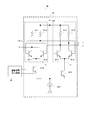
- FIG. 6 is a circuit diagram showing a configuration of the injection locked frequency divider according to the first embodiment of the present invention. This embodiment can be applied to an injection-locked frequency divider mounted on a PLL circuit.
- the injection-locked frequency divider 100 includes a ring oscillator 140 in which a first amplifier circuit 141, a second amplifier circuit 142, and a third amplifier circuit 143 are cascade-connected in three stages, and an N channel.
- the configuration includes a MOS transistor 150 and a differential signal injection circuit 160.
- the first amplifier circuit 141 includes an N-channel MOS transistor 111 and a P-channel MOS transistor 112. In the N-channel MOS transistor 111, the feedback output of the third amplifier circuit 143 is input to the gate.
- the P-channel MOS transistor 112 functions as a load.
- the second amplifier circuit 142 includes an N-channel MOS transistor 121 and a P-channel MOS transistor 122.
- the output of the first amplifier circuit 141 is input to the gate.
- P-channel MOS transistor 122 functions as a load.
- the third amplifier circuit 143 includes an N-channel MOS transistor 131 and a P-channel MOS transistor 132.
- the output of the second amplifier circuit 142 is input to the gate.
- P-channel MOS transistor 132 functions as a load.
- the drain of the N-channel MOS transistor 150 is connected to the sources of the N-channel MOS transistors 111, 121, and 131.
- the differential signal injection circuit 160 outputs an injection signal X1 to the gates of the P-channel MOS transistors 112, 122, and 132 at each stage.
- the differential signal injection circuit 160 outputs a negative phase signal Y1 of the injection signal X1 to the gate of the N-channel MOS transistor 150 as a differential signal.
- the sources of the P-channel MOS transistors 112, 122, 132 are connected to the high potential power supply Vdd.
- the source of the N channel MOS transistor 150 is grounded.
- the drain of the N-channel MOS transistor 131 of the third amplifier circuit 143 and the drain of the P-channel MOS transistor 132 are connected to provide an output of the ring oscillator 140.
- the injection-locked frequency divider 100 of the present embodiment solves the problem that the operating frequency band of the injection-locked frequency divider 10 (FIG. 1) of Non-Patent Document 1 is narrowed.
- the injection-locked frequency divider 100 also inputs a signal to the sources of the N-channel MOS transistors 111, 121, 131 of the amplification circuit of each stage of the ring oscillator 140. To do. With this configuration, the influence of parasitic capacitance can be reduced.
- Patent Document 1 the configuration of an injection-locked frequency divider that inputs a signal from the source of an N-channel MOS transistor is disclosed in Patent Document 1.
- FIG. 7 is a circuit diagram showing a configuration of the injection-locked frequency divider 60 described in Patent Document 1.
- the injection locked frequency divider 60 includes a ring oscillator 70 in which a fourth amplifier circuit 71 and a fifth amplifier circuit 72 are cascade-connected in two stages in a ring shape, a differential signal injection circuit 80, It is the structure containing these.
- the fourth amplifier circuit 71 includes an N-channel BJT (Bipolar Junction Transistor) type differential transistor pair Q11 and Q12 and resistors R11 and R12.
- BJT Bipolar Junction Transistor
- the N channel BJT type differential transistor pair Q11, Q12 receives the feedback output of the fifth amplifier circuit 72 as a base.
- Resistors R11 and R12 function as a load
- the fifth amplifier circuit 72 includes an N-channel BJT type differential transistor pair Q13 and Q14 and resistors R13 and R14.
- the output of the fourth amplifier circuit 71 is input to the base.
- Resistors R13 and R14 function as a load
- the ring oscillator 70 is supplied with a current from the constant current source CS1 through the differential transistor pair Q15 and Q16.
- the differential signal injection circuit 80 is connected to the bases of the differential transistor pair Q15 and Q16 and receives a differential signal.
- the resistors R11, R12, R13, and R14 are connected to the high potential power supply Vdd.
- FIG. 8 is a diagram showing the frequency relationship of the output signal of the injection locking type frequency divider 60.
- an output signal I2' (solid line) is generated near the free-run frequency fo.
- the output signal I2 ′ (solid line) is a signal obtained by down-converting the injection signal I1 ′ by mixing the injection signal I1 ′ and the oscillation signal F1 ′.
- the oscillation signal F1 'of the ring oscillator 70 is attracted to and synchronized with the frequency of the output signal I2'.
- the injection signal I1 ' which phase near the frequency 2fo is in a differential relationship, the injection signal I1' is down-converted into an output signal I2 'near the free-run frequency fo. Therefore, it operates as a frequency divider that divides the frequency by half.
- FIG. 9 shows the phase relationship of the oscillation signal F 1 ′ at each stage of the ring oscillator 70.
- FIG. 9 is a diagram showing a phase relationship at the collector output of each N-channel BJT type transistor of the ring oscillator 70.
- the phase relationship of the second-order harmonic components is twice the oscillation signal F1 'at each stage.
- the phase relationship of the second stage with respect to the first stage is differential of 0 ° and ⁇ 180 °, respectively.
- the injection signal I1 ' may be input through the differential transistor pair Q15 and Q16 as long as the phase relationship of the second stage is differential with respect to the first stage.
- the phase relationship of the frequency signal that is an even multiple of the oscillation frequency fo of the ring oscillator 70 is 0 ° at the first stage and the second stage at ⁇ 180. It is a differential of °. Therefore, the injection locking frequency divider 60 can operate as an even frequency divider by inputting a frequency signal that is an even multiple of the oscillation frequency fo.
- a frequency signal that is an even multiple of the oscillation frequency fo is input from the differential signal injection circuit 80 via the differential transistor pair Q15 and Q16.
- phase relationship of the frequency signal that is an odd multiple of the oscillation frequency fo of the ring oscillator 70 is the same for each of the first-stage N-channel BJT transistors Q11 and Q12 and the second-stage N-channel BJT transistors Q13 and Q14. , Have different phase relationships.
- phase relationships of Q11, Q12, Q13, and Q14 are 0 °, ⁇ 180 °, ⁇ 270 °, and ⁇ 90 °, respectively.
- a differential transistor pair is added between the amplifier circuits 71 and 72 and the constant current source CS1.
- a power source having a higher potential which is not suitable for lowering voltage and lowering power consumption.
- the injection-locked frequency divider 10 of Non-Patent Document 1 has a problem that the injection-locked frequency divider 10 has a problem of reducing the influence of the parasitic capacitance generated between the wiring and the substrate and has a wide operating frequency. Realize.
- differential signals are input to the gates of the P-channel MOS transistors 112, 122, and 132 and the gate of the N-channel MOS transistor 150 of the constant current source.
- the injection-locked frequency divider 100 can be configured by adding one transistor, and an odd-numbered frequency divider that can operate even with a low-voltage power supply can be realized.
- FIG. 10 is a diagram showing a phase relationship in which the injection signal of the injection-locking frequency divider 100 transitions until it is transmitted to the output.
- the signal X1, signal X2, signal Y1, signal Y2, signal Y3, and signal Z1 in FIG. 10 indicate the signal X1, signal X2, signal Y1, signal Y2, signal Y3, and signal Z1 in each part of FIG.
- the differential signal injection circuit 160 outputs the signal X1 to the gates of the P-channel MOS transistors 112, 122, and 132 at each stage, and outputs a differential signal Y1 having a phase opposite to that of the signal X1 to N. Output to the gate of channel MOS transistor 150.
- the signal X ⁇ b> 2, the signal Y ⁇ b> 2, and the signal Y ⁇ b> 3 are signals of each part of the third amplifier circuit 143 that is an output stage, and the signal Z ⁇ b> 1 is an output signal of the injection locked frequency divider 100.
- the output of the ring oscillator 140 is an oscillation having a free-run frequency fo.
- a signal F1 (broken line), a second harmonic component F2 having a frequency 2fo (broken line), and a third harmonic component F3 having a frequency 3fo (broken line) are generated.
- the signal X1 from the differential signal injection circuit 160 is input to the gates of the P-channel MOS transistors 112, 122, and 132 of the ring oscillator 140.
- the drain of the P-channel MOS transistor 132 at the output stage of the ring oscillator 140 outputs a signal X2.
- the signal X2 is an amplified signal obtained by inverting the signal X1.
- the signal input to the gate of the N-channel MOS transistor 150 is output via the signal Y1, the signal Y2, and the signal Y3. Since the inversion is repeated twice at each stage, the signal Y3 is in phase with the signal Y1.
- the signal Z1 that is the output of the ring oscillator 140 (that is, the output of the injection locking frequency divider 100) is a signal output that is the sum of the signal X2 and the signal Y3. As shown in FIG. 10, since the signal X1 and the signal Y3 are in phase, the signal Z1 becomes a signal having a large amplitude by addition.
- Injection locking frequency divider 100 can compensate for the attenuation of output signal Z1 by increasing the signal level of output signal Z1 using signals X2 and Y3.
- an output signal I2 in which the injection signal I1 is down-converted near the free-run frequency F1 (fo) is generated.
- the free run frequency F1 (broken line) of the ring oscillator 140 is attracted to and synchronized with the frequency of the output signal I2 (solid line).
- the output signal I2 corresponds to the output signal Z1 in FIG.
- the injection signal I1 is not easily attenuated even if a parasitic capacitance component is generated, the amplitude of the output signal I2 to be down-converted is increased, and the operation frequency of the injection-locking frequency divider is wide. Turn into.
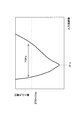
- FIG. 11 is a diagram showing the frequency characteristics of the voltage amplitude of the injection signal I1 from the differential signal injection circuit 160 necessary to stably synchronize the injection locked frequency divider 100.
- the minimum value of the voltage amplitude of the operable injection signal is around 3 times the free-run frequency fo.
- the ring oscillator 140 can operate in a wide frequency band of about 7 GHz at a voltage amplitude of 200 mVpp.
- the frequency band can be expanded by about 2 GHz.
- the injection locked frequency divider 100 includes a ring in which the first amplifier circuit 141, the second amplifier circuit 142, and the third amplifier circuit 143 are cascade-connected in three stages.
- the configuration includes an oscillator 140, an N-channel MOS transistor 150, and a differential signal injection circuit 160.
- the first amplifier circuit 141 includes an N-channel MOS transistor 111 and a P-channel MOS transistor 112. In the N-channel MOS transistor 111, the feedback output of the third amplifier circuit 143 is input to the gate.
- the P-channel MOS transistor 112 functions as a load.
- the second amplifier circuit 142 includes an N-channel MOS transistor 121 and a P-channel MOS transistor 122.
- the output of the first amplifier circuit 141 is input to the gate.
- P-channel MOS transistor 122 functions as a load.
- the third amplifier circuit 143 includes an N-channel MOS transistor 131 and a P-channel MOS transistor 132.
- the output of the second amplifier circuit 142 is input to the gate.
- P-channel MOS transistor 132 functions as a load.
- the drain of the N-channel MOS transistor 150 is connected to the sources of the N-channel MOS transistors 111, 121, 131 at each stage.
- the differential signal injection circuit 160 outputs an injection signal I1 to the gates of the P-channel MOS transistors 112, 122, 132 at each stage.
- the differential signal injection circuit 160 outputs a reverse phase signal of the injection signal I1 as a differential signal to the gate of the N-channel MOS transistor 150.
- differential signals are input to the gates of the P-channel MOS transistors 112, 122, and 132 and the gate of the N-channel MOS transistor 150 that is a constant current source.
- the injection-locked frequency divider 100 uses the differential signal injection circuit 160 and the first N-channel MOS transistor 150 to strengthen the injection signal. That is, as shown by the signal Z1 in FIG. 10, the differential signal input from the differential signal injection circuit 160 becomes in-phase and strengthens at the output stage of the ring oscillator 140. For this reason, the influence of the parasitic capacitance can be reduced, and a wide band operating frequency can be secured. In FIG. 6, it is possible to realize an injection-locked frequency divider that divides the frequency by 1/3 with a wide operating frequency.
- the injection-locked frequency divider 100 can be configured by adding one transistor, and can realize an odd-numbered frequency divider that can operate even with a low-voltage power supply.
- the injection-locked frequency divider 100 is particularly effective when the input is a differential signal and the output is a single signal, and a frequency divider that can operate in a wide band without increasing the circuit scale. Can be realized.
- the number of stages of the ring oscillator 140 has been described as three.
- the present invention is not limited to this, and the number of stages of the ring oscillator 140 is (2n + 1), and the frequency of the injection signal from the differential signal injection circuit 160 May be configured to be around m (2n + 1) times the free-run frequency fo of the ring oscillator.
- the number of stages of the ring oscillator may be five, and the differential signal injection circuit 160 may output a signal having a frequency approximately 5 times or 10 times the oscillation frequency of the five-stage ring oscillator. It can be operated as an injection-locked frequency divider that divides m (2n + 1), and a similar effect can be obtained.
- the free-run frequency fo of the ring oscillator 140 can be adjusted by controlling the bias voltage of the gates of the P-channel MOS transistors 112, 122, and 132 of the ring oscillator 140.
- the ring oscillator 140 may be any ring connected in an odd number of stages, and there is no restriction on the gate type such as a NAND or NOR configuration that functions as an inverter, and the same operation is possible. .
- FIG. 12 is a circuit diagram showing a configuration of an injection locked frequency divider according to the second embodiment of the present invention.
- the same components as those in FIG. 6 are denoted by the same reference numerals, and description of overlapping portions is omitted.
- the injection-locked frequency divider 200 includes a ring oscillator 140 in FIG. 6 (referred to as a first ring oscillator 140 for convenience of explanation) and a second ring having the same configuration as the first ring oscillator 140.
- a ring oscillator 240 and a current source 250 are included.
- the current source 250 includes N-channel MOS transistors 251, 252, and 253.
- the N-channel MOS transistors 251, 252, and 253 are connected to the drains by combining the sources of the N-channel MOS transistors in each stage of the first and second ring oscillators 140 and 240, respectively.
- the injection-locked frequency divider 200 inputs the injection signal X1 to the gates of the P-channel MOS transistors 112, 122, 132 of the first ring oscillator 140, and the P-channel MOS type of the second ring oscillator 240.
- the differential signal injection circuit 160 is configured to input a negative phase signal Y1 of the injection signal X1 as a differential signal to the gates of the transistors 212, 222, and 232.
- the second ring oscillator 240 is a three-stage cascade connection of the first amplifier circuit 241, the second amplifier circuit 242, and the third amplifier circuit 243 in a ring shape.
- the first amplifier circuit 241 includes an N-channel MOS transistor 211 and a P-channel MOS transistor 212.
- N-channel MOS transistor 211 receives the feedback output of third amplifier circuit 243 at its gate.
- the P-channel MOS transistor 212 is a load.
- the second amplifier circuit 242 includes an N-channel MOS transistor 221 and a P-channel MOS transistor 222.
- N-channel MOS transistor 221 receives the output of first amplifier circuit 241 at its gate.
- the P-channel MOS transistor 222 is a load.
- the third amplifier circuit 243 includes an N-channel MOS transistor 231 and a P-channel MOS transistor 232.
- N-channel MOS transistor 231 receives the output of second amplifier circuit 242 at its gate.
- the P-channel MOS transistor 232 is a load.
- the sources of the P-channel MOS transistors 112, 122, 132, 212, 222, and 232 at the respective stages of the first and second ring oscillators 140 and 240 are connected to the high potential power supply Vdd. Further, the bias voltage Vg is supplied to the gates of the N-channel MOS transistors 251, 252, and 253 of the current source 250, and the source is grounded.
- the drain of the N-channel MOS transistor 231 and the drain of the P-channel MOS transistor 232 of the third amplifier circuit 243 of the second ring oscillator 240 are connected to provide an output of the injection locked frequency divider 200.
- FIG. 13 is a diagram showing a phase relationship in which the injection signal of the injection-locked oscillator 200 transitions until it is transmitted to the output.
- Signal X1, signal X2, signal X3, signal X4, signal Y1, signal Y2, and signal Z1 in FIG. 13 are signal X1, signal X2, signal X3, signal X4, signal Y1, signal Y2, and signal Z1 in each part of FIG. Indicates.
- the differential signal injection circuit 160 outputs the signal X1 to the gates of the P-channel MOS transistors 112, 122, and 132 in each stage of the first ring oscillator 140, and has the opposite phase of the signal X1.
- the differential signal Y 1 is output to the gates of the P-channel MOS transistors 212, 222, and 232 of the second ring oscillator 240.
- 12 and 13 are the source potentials of the N-channel MOS transistors 131 and 231 of the third amplifier circuits 143 and 243 of the first and second ring oscillators 140 and 240, respectively.
- the output of the second ring oscillator 240 is free-running frequency fo.
- Oscillation signal F1 (broken line)
- a second harmonic component F2 (broken line) having a frequency 2fo
- a third harmonic component F3 (broken line) having a frequency 3fo are generated.
- the phase relationship is changed until the injection signals X1 and Y1 are transmitted to the output of the ring oscillator 240. Is shown in FIG. 13 and has the same phase in each stage of the second ring oscillator 240.
- Signals input to the gates of the P-channel MOS transistors 112, 122, 132 of the first ring oscillator 140 are output via signals X1 to X4.
- the phase since the phase is inverted twice before transmission from the signal X1 to the signal X2, the phase does not change.
- the first and second ring oscillators 140 and 240 are connected by a constant current source 250, and the signal X2 and the signal X3 are in a differential relationship, so the phase is inverted. Further, the phase is inverted from signal X3 to signal X4.
- signals input to the gates of the P-channel MOS transistors 212, 222, and 232 of the second ring oscillator 240 are output via signals Y1 and Y2.
- the signal Y1 is inverted and amplified.
- the injection-locked frequency divider 200 of the present embodiment has a differential configuration in which the first and second ring oscillators 140 and 240 use the current source 250. Therefore, the injection-locked frequency divider 200 can reduce the influence of the parasitic component, and can realize an injection-locked frequency divider that divides the frequency by 1/3 with a wide operating frequency. it can.
- the injection-locked frequency divider 200 is particularly effective when the input signal is a differential signal and the output signal is a differential signal or a single signal, and a frequency at which broadband operation is possible.
- a frequency divider can be realized.
- the N-channel MOS transistors 251, 252, and 253 are used as the constant current source 250.
- a passive element including a resistor or an inductor is used, an injection-locked frequency divider is used. It can be operated. By using passive elements, a simpler and smaller circuit configuration can be realized.
- the number of stages of the first and second ring oscillators 140 and 240 has been described as three, as in the first embodiment, but the present invention is not limited to this, and the first and second The number of stages of the ring oscillators 140 and 240 may be (2n + 1) stages, and the frequency of the injection signal from the differential signal injection circuit 160 may be close to m (2n + 1) times the free-run frequency fo of the ring oscillator. As a result, it can be operated as an injection-locked frequency divider that divides m (2n + 1), and a similar effect can be obtained.
- the free-run frequency of the ring oscillators 140 and 240 is controlled by controlling the bias voltage of the gates of the P-channel MOS transistors 112, 122, 132, 212, 222, and 232 of the ring oscillators 140 and 240. fo can be adjusted.
- FIG. 14 is a circuit diagram showing a configuration of an injection locked frequency divider according to the third embodiment of the present invention.
- the same components as those in FIG. 12 are denoted by the same reference numerals, and description of overlapping portions is omitted.
- the injection-locked frequency divider 300 includes a first ring oscillator 140, a second ring oscillator 240 having the same configuration as the first ring oscillator 140, and an N-channel MOS type that is a current source.
- the configuration includes a transistor 350 and a differential signal injection circuit 160.
- the N-channel MOS transistor 350 as a current source is connected to the drain by combining the sources of the N-channel MOS transistors 131 and 231 at the output stage of the first and second ring oscillators 140 and 240.
- the differential signal injection circuit 160 outputs an injection signal I1 to the gates of the P-channel MOS transistors 112, 122, 132 of the first ring oscillator 140, and the P-channel MOS transistor 212 of the second ring oscillator 240. , 222, 232, the opposite phase signal of the injection signal I1 is output as a differential signal.
- the injection-locked frequency divider 300 is different from the injection-locked frequency divider 200 of FIG. 12 in that an N-channel MOS transistor 350 as a current source is connected only to the output stage.
- the output of the second ring oscillator 240 includes the oscillation signal F1 (dashed line) having the free-run frequency fo, the frequency A second-order harmonic component F2 (dashed line) having 2fo and a third-order harmonic component F3 (dashed line) having a frequency 3fo are generated.
- the injection signal from the differential signal injection circuit 160 is input with the injection signals X1 and Y1 having a frequency of about 3 fo, the signal via the P-channel MOS transistor of the first ring oscillator 140, the second Since the signal via the P-channel MOS transistor of the ring oscillator 240 is in phase with the output of the injection locked frequency divider 300, the amplitude increases.
- the attenuation of the injection signal due to the parasitic capacitance component can be compensated. That is, even if the injection signal is attenuated by the parasitic capacitance component, the attenuation of the injection signal is compensated by increasing the amplitude of the signal level at the output of the injection locking frequency divider 300.
- phase relationship of each stage of the first and second ring oscillators 140 and 240 includes a phase rotation of 120 °. Note that it is possible to operate even when the rotation directions are opposite to each other.
- the injection-locked frequency divider 300 of the present embodiment has a differential configuration using the current source 350 at the output stage of the first and second ring oscillators 140 and 240. For this reason, the number of MOS transistors used as the current source 350 can be reduced. As a result, the influence of parasitic components can be reduced without increasing the circuit scale, and an injection-locked frequency divider that divides the frequency by 1/3 with a wide operating frequency can be realized.
- the injection-locked frequency divider 300 of this embodiment is particularly effective when the input signal is a differential signal and the output signal is a differential signal or a single signal, and has a wide bandwidth without increasing the circuit scale.
- a frequency divider capable of operation can be realized.
- the output stage of the amplification circuits of the first and second ring oscillators 140 and 240 has a differential configuration using the current source 350.
- the present invention is not limited to this, and other than the output stage Other amplifier circuits may have a differential configuration. The effect of expanding the degree of freedom of design can be expected.
- the N-channel MOS transistor 350 is used as a current source.
- a passive element including a resistor or an inductor it can be operated as an injection-locked frequency divider. By using passive elements, a simpler and smaller circuit configuration can be realized.
- the first and second ring oscillators 140 and 240 are described as having three stages. However, the present invention is not limited to this, and the first and second ring oscillators are not limited thereto.
- the number of stages of the ring oscillators 140 and 240 may be (2n + 1) stages, and the frequency of the injection signal from the differential signal injection circuit 160 may be close to m (2n + 1) times the free-run frequency fo of the ring oscillator. It can be operated as an injection-locked frequency divider that divides m (2n + 1), and a similar effect can be obtained.
- the free-run frequency of the ring oscillators 140 and 240 is controlled by controlling the bias voltage of the gates of the P-channel MOS transistors 112, 122, 132, 212, 222, and 232 of the ring oscillators 140 and 240. fo can be adjusted.
- FIG. 15 is a diagram showing a configuration of a fixed frequency dividing circuit (prescaler) according to the fourth exemplary embodiment of the present invention.
- the fixed frequency dividing circuit 400 includes the injection-locked frequency divider 100 and the fixed frequency divider 460 shown in FIG. 6.
- the high frequency differential signal is frequency-divided into a single output signal by the injection locking type frequency divider 100.
- the single output signal is further frequency-divided to a low frequency by a fixed frequency divider 460.
- the fixed frequency dividing circuit 400 of the present embodiment is configured by using the injection locking type frequency divider 100 of the first embodiment as the injection locking type frequency dividing device 100 of the fixed frequency dividing circuit. Since the output of the injection locked frequency divider 100 and the input of the fixed divider 460 at the subsequent stage can be configured using a single output signal, the operating frequency is not only wideband, but also small and low consumption. A power fixed frequency dividing circuit can be realized.
- FIG. 16 is a diagram showing a configuration of a PLL circuit according to the fifth embodiment of the present invention.
- the PLL circuit 500 includes the injection-locked frequency divider 100 of FIG. 6 (or one of the injection-locked frequency divider 200 of FIG. 12 and the injection-locked frequency divider 300 of FIG. 14). , Reference signal oscillator 410, voltage controlled oscillator 420, phase frequency comparator 430, charge pump 440, and loop filter 450.
- the voltage controlled oscillator 420 outputs a high frequency signal.
- the high frequency signal is frequency-divided to a low frequency by the injection locking type frequency divider 100 (200, 300).
- the phase frequency comparator 430 compares the frequency-divided signal of the injection-locking frequency divider 100 (200, 300) with the output signal of the reference signal oscillator 410, and outputs a phase and frequency error to the charge pump 440.
- the charge pump 440 converts the phase and frequency error detected by the phase frequency comparator 430 into a current, and the loop filter 450 generates a control voltage for the voltage controlled oscillator 420.
- the control voltage operates as a PLL circuit that performs a frequency negative feedback operation in order to control the voltage controlled oscillator 420 so that an error detected by the phase frequency comparator 430 is reduced.
- the PLL circuit 500 of the present embodiment is configured by using the injection-locked frequency divider 100 (200, 300) of the first to third embodiments as the injection-locked frequency divider of the PLL circuit. Yes. Since the operating frequency band of the injection locking frequency divider 100 (200, 300) is wide, a PLL circuit having a wide operating frequency can be realized.
- the injection-locking frequency divider 100 (200, 300) is an odd-numbered frequency divider and has a larger frequency division number than that of the two-frequency divider, the number of frequency dividers as a PLL circuit can be reduced. A small and low power consumption PLL circuit can be realized.
- a fixed frequency divider or a frequency divider including a programmable counter is connected between the injection locking frequency divider 100 (200, 300) and the phase frequency comparator 430 to divide the frequency to a low frequency. Has the same effect.
- MOS transistor Metal Insulated Semiconductor
- SOI Silicon-On-Insulator
- bipolar transistor Bi-CMOS, or a combination thereof may be used.
- MOS transistors are advantageous in terms of power consumption.
- injection-locked frequency divider is used in each of the above embodiments, this is for convenience of explanation, and it goes without saying that it may be a frequency divider, a PLL device, or the like.
- the circuit parts constituting the injection-locked frequency divider for example, the number of inverter gate stages of the ring oscillator, the type of logic element, etc. are not limited to the above-described embodiment. Needless to say, various compensation transistors may be added to the injection-locked frequency divider.
- the injection-locked frequency divider and PLL circuit according to the present invention can be used for an injection-locked frequency divider and PLL circuit used in portable communication terminals, and in particular, can divide a frequency signal of 10 GHz or more. This is useful for a wide bandwidth injection-locked frequency divider and PLL circuit. Further, it can be applied to all electronic circuits as an injection-locked frequency divider.
Landscapes
- Engineering & Computer Science (AREA)
- Power Engineering (AREA)
- Stabilization Of Oscillater, Synchronisation, Frequency Synthesizers (AREA)
Abstract
Description
図6は、本発明の実施の形態1に係る注入同期型分周器の構成を示す回路図である。本実施の形態は、PLL回路に搭載される注入同期型分周器に適用可能である。
図12は、本発明の実施の形態2に係る注入同期型分周器の構成を示す回路図である。図6と同一構成部分には同一符号を付して重複箇所の説明を省略する。
図14は、本発明の実施の形態3に係る注入同期型分周器の構成を示す回路図である。図12と同一構成部分には同一符号を付して重複箇所の説明を省略する。
図15は、本発明の実施の形態4に係る固定分周回路(プリスケーラ)の構成を示す図である。
図16は、本発明の実施の形態5に係るPLL回路の構成を示す図である。
111,121,131,150,212,222,232,251,252,253,350 NチャネルMOS型トランジスタ
112,122,132,212,222,232 PチャネルMOS型トランジスタ
140,240 リング発振器
141 第1増幅回路
142 第2増幅回路
143 第3増幅回路
160 差動信号注入回路
250 電流源
400 固定分周回路
410 基準信号発振器
420 電圧制御発振器
430 位相周波数比較器
440 チャージポンプ
450 ループフィルタ
500 PLL回路
Claims (4)
- NチャネルMOS型トランジスタとPチャネルMOS型トランジスタとを含む増幅回路をリング状に(2n+1)(nは任意の自然数)段縦続接続したリング発振器と、
前記リング発振器に接続され、前記リング発振器を駆動させるNチャネルMOS型トランジスタからなる電流源と、
前記リング発振器に注入信号を出力し、前記電流源に前記注入信号の逆相信号を差動信号として出力する差動信号注入回路と、
を備え、
前記電流源の前記NチャネルMOS型トランジスタのドレインは、前記リング発振器のNチャネルMOS型トランジスタのソースに接続し、
前記差動信号注入回路は、前記リング発振器のPチャネルMOS型トランジスタのゲートに前記注入信号を出力し、かつ、前記電流源の前記NチャネルMOS型トランジスタのゲートに前記差動信号を出力する、
注入同期型分周器。 - 前記リング発振器の出力段は、前記注入信号を基に増幅した信号と前記差動信号を基に増幅した信号とを同相で重ね合わせて出力する請求項1記載の注入同期型分周器。
- 前記差動信号注入回路は、前記リング発振器の発振周波数のm(2n+1)(mは任意の自然数)倍の周波数の信号を注入する請求項1記載の注入同期型分周器。
- 基準信号を出力する基準信号発振器と、
高周波信号を出力する電圧制御発振器と、
前記高周波信号を分周する注入同期型分周器と、
前記注入同期型分周器の分周と前記基準信号発振器の出力信号とを比較し、位相と周波数の誤差を出力する位相周波数比較器と、
前記位相周波数比較器により検波された位相と周波数の誤差を電流に変換するチャージポンプと、
前記電圧制御発振器の制御電圧を生成し、生成した制御電圧を前記電圧制御発振器に出力するループフィルタとを備え、前記制御電圧は、前記位相周波数比較器で検波される誤差が小さくなるように前記電圧制御発振器を制御する、周波数負帰還動作を行うPLL回路であって、
前記注入同期型分周器は、請求項1に記載の注入同期型分周器であるPLL回路。
Priority Applications (4)
| Application Number | Priority Date | Filing Date | Title |
|---|---|---|---|
| US13/266,160 US8466721B2 (en) | 2010-01-22 | 2011-01-21 | Injection locked frequency divider and PLL circuit |
| EP11734525.6A EP2528232B1 (en) | 2010-01-22 | 2011-01-21 | Injection-locked frequency divider and pll circuit |
| JP2011519541A JP5480896B2 (ja) | 2010-01-22 | 2011-01-21 | 注入同期型奇数分周器及びpll回路 |
| CN201180001435.2A CN102356547B (zh) | 2010-01-22 | 2011-01-21 | 注入锁定分频器、以及锁相环电路 |
Applications Claiming Priority (2)
| Application Number | Priority Date | Filing Date | Title |
|---|---|---|---|
| JP2010-012131 | 2010-01-22 | ||
| JP2010012131 | 2010-01-22 |
Publications (1)
| Publication Number | Publication Date |
|---|---|
| WO2011089918A1 true WO2011089918A1 (ja) | 2011-07-28 |
Family
ID=44306721
Family Applications (1)
| Application Number | Title | Priority Date | Filing Date |
|---|---|---|---|
| PCT/JP2011/000317 Ceased WO2011089918A1 (ja) | 2010-01-22 | 2011-01-21 | 注入同期型分周器及びpll回路 |
Country Status (5)
| Country | Link |
|---|---|
| US (1) | US8466721B2 (ja) |
| EP (1) | EP2528232B1 (ja) |
| JP (2) | JP5480896B2 (ja) |
| CN (2) | CN103997318B (ja) |
| WO (1) | WO2011089918A1 (ja) |
Cited By (3)
| Publication number | Priority date | Publication date | Assignee | Title |
|---|---|---|---|---|
| JPWO2014136399A1 (ja) * | 2013-03-05 | 2017-02-09 | パナソニック株式会社 | 注入同期型発振器 |
| US9847785B2 (en) | 2014-03-13 | 2017-12-19 | Mitsubishi Electric Corporation | Phase locked loop circuit and method of frequency adjustment of injection locked frequency divider |
| JP2024524968A (ja) * | 2021-06-28 | 2024-07-09 | クアルコム,インコーポレイテッド | リング発振器に基づく分周器 |
Families Citing this family (14)
| Publication number | Priority date | Publication date | Assignee | Title |
|---|---|---|---|---|
| US9099956B2 (en) | 2011-04-26 | 2015-08-04 | King Abdulaziz City For Science And Technology | Injection locking based power amplifier |
| JP5761232B2 (ja) * | 2013-03-01 | 2015-08-12 | ソニー株式会社 | 受信装置および電子機器 |
| US9106234B2 (en) | 2013-03-15 | 2015-08-11 | Qualcomm Incorporated | Programmable frequency divider for local oscillator generation |
| WO2015042814A1 (en) * | 2013-09-25 | 2015-04-02 | Huawei Technologies Co., Ltd. | Wideband injection locked frequency multipliers, oscillators and dividers using higher order lc resonant tank |
| US9219486B2 (en) * | 2013-11-18 | 2015-12-22 | California Institute Of Technology | Quadrature-based injection locking of ring oscillators |
| CN104579319B (zh) * | 2014-04-22 | 2019-04-09 | 上海华虹宏力半导体制造有限公司 | 多相位时钟生成器 |
| CN105262484B (zh) * | 2015-11-17 | 2018-04-24 | 中山大学 | 实现环形振荡器注入锁定的方法及其电路 |
| US10411716B2 (en) | 2016-06-06 | 2019-09-10 | Richwave Technology Corp. | Subsampling motion detector for detecting motion of object under measurement |
| US10942255B2 (en) * | 2018-10-11 | 2021-03-09 | Globalfoundries U.S. Inc. | Apparatus and method for integrating self-test oscillator with injection locked buffer |
| CN109560774B (zh) * | 2018-11-28 | 2021-09-14 | 电子科技大学 | 一种能在不同频段实现不同分频比功能的注入锁定分频器 |
| TWI726791B (zh) | 2019-08-14 | 2021-05-01 | 創未來科技股份有限公司 | 訊號除頻器、訊號分佈系統與其相關方法 |
| US10715038B1 (en) * | 2019-11-29 | 2020-07-14 | Realtek Semiconductor Corp. | Apparatus and method for frequency quintupling |
| JP2023182368A (ja) * | 2022-06-14 | 2023-12-26 | キオクシア株式会社 | 半導体集積回路、pll回路及び信号処理装置 |
| WO2024005813A1 (en) * | 2022-06-30 | 2024-01-04 | Intel Corporation | Apparatus, system, and method of local oscillator (lo) generator |
Citations (4)
| Publication number | Priority date | Publication date | Assignee | Title |
|---|---|---|---|---|
| JPH0548402A (ja) * | 1991-08-19 | 1993-02-26 | Nippon Telegr & Teleph Corp <Ntt> | スタテイツク型フリツプフロツプ回路 |
| JPH09246957A (ja) * | 1996-03-08 | 1997-09-19 | Toshiba Corp | 分周器 |
| JPH1093399A (ja) | 1996-09-19 | 1998-04-10 | Toshiba Corp | 注入同期リング発振器 |
| JP2010012131A (ja) | 2008-07-07 | 2010-01-21 | Toshiba Corp | 超音波診断装置 |
Family Cites Families (16)
| Publication number | Priority date | Publication date | Assignee | Title |
|---|---|---|---|---|
| JPS628602A (ja) * | 1985-07-05 | 1987-01-16 | Nec Corp | マイクロ波アナログ分周器 |
| JP4017352B2 (ja) * | 2001-03-16 | 2007-12-05 | 三菱電機株式会社 | 光モジュール |
| DE60328925D1 (de) * | 2002-12-24 | 2009-10-01 | Fujitsu Microelectronics Ltd | Jittergenerator |
| JP4532847B2 (ja) * | 2003-05-16 | 2010-08-25 | 株式会社リコー | 差動増幅器 |
| US6989697B2 (en) * | 2004-01-15 | 2006-01-24 | Organicid, Inc. | Non-quasistatic phase lock loop frequency divider circuit |
| TWI233728B (en) * | 2004-05-06 | 2005-06-01 | Realtek Semiconductor Corp | Injection-locked frequency divider and frequency dividing method thereof |
| WO2006117860A1 (ja) * | 2005-04-28 | 2006-11-09 | Thine Electronics, Inc. | 差動駆動回路およびそれを内蔵する電子機器 |
| JP4195702B2 (ja) * | 2005-07-08 | 2008-12-10 | 株式会社ルネサステクノロジ | クロック同期回路 |
| JP4356659B2 (ja) * | 2005-07-12 | 2009-11-04 | ソニー株式会社 | 電圧制御型発振回路およびpll回路 |
| US20070120588A1 (en) * | 2005-11-30 | 2007-05-31 | Lim Chee H | Low-jitter clock distribution |
| JP4646856B2 (ja) * | 2006-06-09 | 2011-03-09 | ルネサスエレクトロニクス株式会社 | 周波数シンセサイザ |
| JP2008054134A (ja) * | 2006-08-25 | 2008-03-06 | Matsushita Electric Ind Co Ltd | リング発振器及びそれを備えた半導体集積回路及び電子機器 |
| WO2009049143A1 (en) * | 2007-10-10 | 2009-04-16 | Georgia Tech Research Corporation | Millimeter-wave wideband voltage controlled oscillator |
| TWI352508B (en) * | 2007-11-30 | 2011-11-11 | Univ Nat Taiwan | Transistor-based voltage-controlled oscillator and |
| WO2010134257A1 (ja) * | 2009-05-21 | 2010-11-25 | パナソニック株式会社 | Cmosインバータ型分周器、及び当該分周器を備える携帯電話 |
| US9054711B2 (en) * | 2009-07-02 | 2015-06-09 | Infineon Technologies Ag | Frequency divider |
-
2011
- 2011-01-21 WO PCT/JP2011/000317 patent/WO2011089918A1/ja not_active Ceased
- 2011-01-21 EP EP11734525.6A patent/EP2528232B1/en not_active Not-in-force
- 2011-01-21 US US13/266,160 patent/US8466721B2/en not_active Expired - Fee Related
- 2011-01-21 JP JP2011519541A patent/JP5480896B2/ja not_active Expired - Fee Related
- 2011-01-21 CN CN201410081843.9A patent/CN103997318B/zh not_active Expired - Fee Related
- 2011-01-21 CN CN201180001435.2A patent/CN102356547B/zh not_active Expired - Fee Related
-
2014
- 2014-02-13 JP JP2014025392A patent/JP5793698B2/ja not_active Expired - Fee Related
Patent Citations (4)
| Publication number | Priority date | Publication date | Assignee | Title |
|---|---|---|---|---|
| JPH0548402A (ja) * | 1991-08-19 | 1993-02-26 | Nippon Telegr & Teleph Corp <Ntt> | スタテイツク型フリツプフロツプ回路 |
| JPH09246957A (ja) * | 1996-03-08 | 1997-09-19 | Toshiba Corp | 分周器 |
| JPH1093399A (ja) | 1996-09-19 | 1998-04-10 | Toshiba Corp | 注入同期リング発振器 |
| JP2010012131A (ja) | 2008-07-07 | 2010-01-21 | Toshiba Corp | 超音波診断装置 |
Cited By (3)
| Publication number | Priority date | Publication date | Assignee | Title |
|---|---|---|---|---|
| JPWO2014136399A1 (ja) * | 2013-03-05 | 2017-02-09 | パナソニック株式会社 | 注入同期型発振器 |
| US9847785B2 (en) | 2014-03-13 | 2017-12-19 | Mitsubishi Electric Corporation | Phase locked loop circuit and method of frequency adjustment of injection locked frequency divider |
| JP2024524968A (ja) * | 2021-06-28 | 2024-07-09 | クアルコム,インコーポレイテッド | リング発振器に基づく分周器 |
Also Published As
| Publication number | Publication date |
|---|---|
| JP5793698B2 (ja) | 2015-10-14 |
| CN102356547B (zh) | 2014-04-09 |
| EP2528232A1 (en) | 2012-11-28 |
| JPWO2011089918A1 (ja) | 2013-05-23 |
| EP2528232A4 (en) | 2016-10-19 |
| CN103997318B (zh) | 2016-08-31 |
| EP2528232B1 (en) | 2018-08-01 |
| CN102356547A (zh) | 2012-02-15 |
| US20120038396A1 (en) | 2012-02-16 |
| CN103997318A (zh) | 2014-08-20 |
| US8466721B2 (en) | 2013-06-18 |
| JP2014123973A (ja) | 2014-07-03 |
| JP5480896B2 (ja) | 2014-04-23 |
Similar Documents
| Publication | Publication Date | Title |
|---|---|---|
| JP5480896B2 (ja) | 注入同期型奇数分周器及びpll回路 | |
| US20200177193A1 (en) | Voltage controlled oscillator based on complementary current-injection field-effect transistor devices | |
| US6535037B2 (en) | Injection locked frequency multiplier | |
| US7298183B2 (en) | High frequency divider circuits and methods | |
| JP6363989B2 (ja) | 注入同期型発振器 | |
| US20080252387A1 (en) | Oscillator | |
| JP5876368B2 (ja) | 改良された帯域幅を備える電圧制御発振器を有する位相同期ループ回路 | |
| JP5372114B2 (ja) | 分周回路およびpll回路 | |
| CN104641560B (zh) | Rf逻辑分频器 | |
| CN101425803A (zh) | 环路压控振荡器 | |
| US20150222270A1 (en) | Frequency dividing circuit and phase synchronization circuit | |
| US9537476B1 (en) | Level shifter with low duty cycle variation | |
| JP5976685B2 (ja) | ラッチディバイダ | |
| JP2021034784A (ja) | 注入同期型分周器 | |
| KR100970132B1 (ko) | 인버터 구조를 갖는 주파수 분배기 | |
| Farazian et al. | Stability and operation of injection-locked regenerative frequency dividers | |
| US7498892B2 (en) | Split-biased interpolated voltage-controlled oscillator and phase locked loop | |
| JP2015082720A (ja) | 発振器および信号処理回路 | |
| CN115425949A (zh) | 压控振荡器及基于其的时钟发生器 | |
| il Kim et al. | A dual band CMOS VCO with a balanced duty cycle buffer | |
| JP2007088885A (ja) | 遅延回路およびそれを用いた電圧制御発振器 | |
| KR20070032201A (ko) | 클록 분배 회로 |
Legal Events
| Date | Code | Title | Description |
|---|---|---|---|
| WWE | Wipo information: entry into national phase |
Ref document number: 201180001435.2 Country of ref document: CN |
|
| WWE | Wipo information: entry into national phase |
Ref document number: 2011519541 Country of ref document: JP |
|
| 121 | Ep: the epo has been informed by wipo that ep was designated in this application |
Ref document number: 11734525 Country of ref document: EP Kind code of ref document: A1 |
|
| WWE | Wipo information: entry into national phase |
Ref document number: 13266160 Country of ref document: US |
|
| WWE | Wipo information: entry into national phase |
Ref document number: 2287/MUMNP/2011 Country of ref document: IN |
|
| WWE | Wipo information: entry into national phase |
Ref document number: 2011734525 Country of ref document: EP |
|
| NENP | Non-entry into the national phase |
Ref country code: DE |