WO2011105185A1 - Procédé de fabrication de module d'élément à semi-conducteur optique - Google Patents
Procédé de fabrication de module d'élément à semi-conducteur optique Download PDFInfo
- Publication number
- WO2011105185A1 WO2011105185A1 PCT/JP2011/052233 JP2011052233W WO2011105185A1 WO 2011105185 A1 WO2011105185 A1 WO 2011105185A1 JP 2011052233 W JP2011052233 W JP 2011052233W WO 2011105185 A1 WO2011105185 A1 WO 2011105185A1
- Authority
- WO
- WIPO (PCT)
- Prior art keywords
- semiconductor element
- optical semiconductor
- sealing
- sheet
- manufacturing
- Prior art date
- Legal status (The legal status is an assumption and is not a legal conclusion. Google has not performed a legal analysis and makes no representation as to the accuracy of the status listed.)
- Ceased
Links
Images




Classifications
-
- H—ELECTRICITY
- H10—SEMICONDUCTOR DEVICES; ELECTRIC SOLID-STATE DEVICES NOT OTHERWISE PROVIDED FOR
- H10H—INORGANIC LIGHT-EMITTING SEMICONDUCTOR DEVICES HAVING POTENTIAL BARRIERS
- H10H20/00—Individual inorganic light-emitting semiconductor devices having potential barriers, e.g. light-emitting diodes [LED]
- H10H20/80—Constructional details
- H10H20/85—Packages
- H10H20/852—Encapsulations
-
- H—ELECTRICITY
- H10—SEMICONDUCTOR DEVICES; ELECTRIC SOLID-STATE DEVICES NOT OTHERWISE PROVIDED FOR
- H10K—ORGANIC ELECTRIC SOLID-STATE DEVICES
- H10K71/00—Manufacture or treatment specially adapted for the organic devices covered by this subclass
- H10K71/10—Deposition of organic active material
- H10K71/12—Deposition of organic active material using liquid deposition, e.g. spin coating
- H10K71/13—Deposition of organic active material using liquid deposition, e.g. spin coating using printing techniques, e.g. ink-jet printing or screen printing
-
- H—ELECTRICITY
- H10—SEMICONDUCTOR DEVICES; ELECTRIC SOLID-STATE DEVICES NOT OTHERWISE PROVIDED FOR
- H10W—GENERIC PACKAGES, INTERCONNECTIONS, CONNECTORS OR OTHER CONSTRUCTIONAL DETAILS OF DEVICES COVERED BY CLASS H10
- H10W72/00—Interconnections or connectors in packages
- H10W72/01—Manufacture or treatment
- H10W72/0198—Manufacture or treatment batch processes
-
- H—ELECTRICITY
- H10—SEMICONDUCTOR DEVICES; ELECTRIC SOLID-STATE DEVICES NOT OTHERWISE PROVIDED FOR
- H10H—INORGANIC LIGHT-EMITTING SEMICONDUCTOR DEVICES HAVING POTENTIAL BARRIERS
- H10H20/00—Individual inorganic light-emitting semiconductor devices having potential barriers, e.g. light-emitting diodes [LED]
- H10H20/01—Manufacture or treatment
- H10H20/036—Manufacture or treatment of packages
- H10H20/0361—Manufacture or treatment of packages of wavelength conversion means
-
- H—ELECTRICITY
- H10—SEMICONDUCTOR DEVICES; ELECTRIC SOLID-STATE DEVICES NOT OTHERWISE PROVIDED FOR
- H10H—INORGANIC LIGHT-EMITTING SEMICONDUCTOR DEVICES HAVING POTENTIAL BARRIERS
- H10H20/00—Individual inorganic light-emitting semiconductor devices having potential barriers, e.g. light-emitting diodes [LED]
- H10H20/01—Manufacture or treatment
- H10H20/036—Manufacture or treatment of packages
- H10H20/0362—Manufacture or treatment of packages of encapsulations
-
- H—ELECTRICITY
- H10—SEMICONDUCTOR DEVICES; ELECTRIC SOLID-STATE DEVICES NOT OTHERWISE PROVIDED FOR
- H10K—ORGANIC ELECTRIC SOLID-STATE DEVICES
- H10K71/00—Manufacture or treatment specially adapted for the organic devices covered by this subclass
- H10K71/40—Thermal treatment, e.g. annealing in the presence of a solvent vapour
-
- H—ELECTRICITY
- H10—SEMICONDUCTOR DEVICES; ELECTRIC SOLID-STATE DEVICES NOT OTHERWISE PROVIDED FOR
- H10K—ORGANIC ELECTRIC SOLID-STATE DEVICES
- H10K71/00—Manufacture or treatment specially adapted for the organic devices covered by this subclass
- H10K71/851—Division of substrate
-
- H—ELECTRICITY
- H10—SEMICONDUCTOR DEVICES; ELECTRIC SOLID-STATE DEVICES NOT OTHERWISE PROVIDED FOR
- H10W—GENERIC PACKAGES, INTERCONNECTIONS, CONNECTORS OR OTHER CONSTRUCTIONAL DETAILS OF DEVICES COVERED BY CLASS H10
- H10W90/00—Package configurations
- H10W90/701—Package configurations characterised by the relative positions of pads or connectors relative to package parts
- H10W90/721—Package configurations characterised by the relative positions of pads or connectors relative to package parts of bump connectors
- H10W90/724—Package configurations characterised by the relative positions of pads or connectors relative to package parts of bump connectors between a chip and a stacked insulating package substrate, interposer or RDL
Definitions
- the present invention relates to a method for manufacturing an optical semiconductor element module.
- the present invention relates to a method of manufacturing an optical semiconductor element module formed and modularized.
- the manufacturing method of these optical semiconductor elements is to form a semiconductor by epitaxial growth on a single crystal substrate, to form a dividing groove that makes this an individual element, and to form an electrode pad at a necessary location. Chip.
- a general manufacturing method is such that electrodes are wire-bonded to the electrode pads, modularized by sealing with resin or the like, and finally packaged for completion (see, for example, Patent Document 1).
- Chip formation is performed by forming divided grooves, electrode pads, and (transparent) electrodes as necessary on the formed semiconductor by photolithography technology and etching technology. After performing such chip formation and wire bonding, it may be cut after being cut into individual elements first, or may be cut after sealing.
- an electrode pad is formed by placing semiconductor chips one by one on a copper plate formed by punching out about 500 wires and wire bonding them.
- resin sealing the resin was injected into a thermosetting resin transfer molding apparatus, and the resin was injected and sealed for about 10 minutes.
- high-brightness LEDs generate a large amount of heat and are sealed with glass.
- semiconductor chips and phosphors are embedded one by one in a glass substrate that is molded by glass molding in about 1 minute / piece, and finally glass.
- a method of covering with a low-melting glass after covering with a plate has been used.
- the number of LED modules that can be completed with one molding device or sealing device is about 20 million pieces / year for resin sealing, and about 1/10 for glass sealing. Even in the case of cutting after sealing, the production amount is almost the same as above.
- the conventional manufacturing process has a disadvantage that the production efficiency is poor because each process must be performed by different apparatuses.
- the process of growing semiconductors must use a vacuum evaporation system or a CVD system, but the subsequent processes may be able to be continued by ingenuity, and if continuous processing is possible in this way, production efficiency Can be greatly improved.
- LED chips In the case of LED chips, etc., there is a problem of heat. LED chips have high conversion efficiency from power to light, but if the current is increased in order to achieve high brightness, a large amount of heat for conversion loss is generated. Moreover, since the LED chip has a small size and a small heat capacity, and the light emitting part is a further small part, heat is concentrated in a very small area together with the light emission, so that it tends to be a high temperature of several hundred degrees Celsius. Therefore, the part that seals the LED chip has a high heat resistance and good heat dissipation (a material with good heat conduction, a large surface area, and a small volume), so that the input current can be increased and light can be emitted with higher brightness. It is advantageous.
- the object of the present invention is to solve the above-described problems, that is, to improve production efficiency by improving the manufacturing process.
- the above purpose is to convey a continuous sheet as a sealing material on one side, and in the order of conveying the continuous sheet, in order to form electrodes on the continuous sheet, to form a spacer, between the spacers
- Producing a sheet on which a plurality of optical semiconductor element modules are formed by arranging a step of chip-on a separately manufactured optical semiconductor element chip and a step of supplying a sealing material on the other side to perform sealing. Achieved by: The created sheet is then cut into individual optical semiconductor modules, but this cutting step may be arranged after the sealing step.
- the manufacturing method is such that the members constituting the optical semiconductor element module are sequentially formed on the continuous sheet, extremely high productivity, low cost, and high quality reliability can be realized. It is.
- the sealing material a sheet-like material may be laminated and adhered, or a liquid material may be applied and dried. In either case, the material or process is configured so as to form a thin sealing film.
- the thickness of the sealing film is 10 ⁇ m to 1000 ⁇ m, more preferably 10 ⁇ m to 500 ⁇ m.
- a thicker sealing material accumulates heat.
- the plastic or glass material may be broken or modified unless the sheet thickness is 1 mm or less, and the metal material may be wrinkled.
- the thickness of the sealing material is reduced to 10 ⁇ m or less, since the strength is weak, there is a concern that the sealing easily breaks and the sealing is broken, so that the thickness is preferably 10 ⁇ m or more.
- sealing materials since the form of these sealing materials is a thin sheet material or coating material, heat is hard to accumulate and heat dissipation is good, so even if the same LED chip as in the past is used, more current can be input, Therefore, high luminance can be realized, and since the transmitted light path length of the emitted light passing through the sealing material is short, a great improvement effect can be obtained that there is little change in color even in the case of sealing with a resin material.
- the object of the present invention can be achieved by the production method described below.
- a method for manufacturing an optical semiconductor element module in which a plurality of optical semiconductor element chips are continuously formed on a module, conveying a continuous sheet as a sealing material on one side of the module, and sequentially in the conveying direction of the continuous sheet, An electrode forming step for forming an electrode connected to the optical semiconductor element chip on the continuous sheet, a spacer forming step for forming a spacer that controls the thickness of each chip, and an optical semiconductor element chip is interposed between the spacers.
- a plurality of optical semiconductor element modules are formed by disposing a chip-on process for chip-on and a sealing process for supplying a sealing material as a sealing material on the other surface on the optical semiconductor element chip to perform sealing.
- a method for producing an optical semiconductor element module comprising: producing a sheet.
- An optical semiconductor element module manufacturing method for continuously forming a plurality of optical semiconductor element chips on a module, wherein an electrode connected to the optical semiconductor element chip is formed on a surface in advance, and a sealing material on one side of the module
- Forming a sheet in which a plurality of optical semiconductor element modules are formed by arranging a sealing step for sealing by supplying a sealing material which becomes a sealing material on the other surface on the optical semiconductor element chip
- a method for manufacturing an optical semiconductor element module for continuously forming a plurality of optical semiconductor element chips on a module, wherein an electrode connected to the optical semiconductor element chip is formed on a surface in advance, and a sealing material on one side of the module
- the sealing step includes a heating unit that heats at a temperature of 30 ° C. or higher and lower than a glass transition point of the spacer material.
- the electrode material in the electrode forming step is any one of conductive ink, transparent conductive ink, and conductive adhesive, and the electrode material is formed on a continuous sheet by printing.
- the manufacturing method of the optical semiconductor element module in any one of.
- the present invention can realize extremely high productivity, low cost, and high quality reliability.
- the sealing material is made of a thin sheet material or coating material, heat is hard to accumulate and heat dissipation is good, so that an optical semiconductor element module excellent in terms of thermal conductivity and heat resistance can be provided.
- FIG. 1A is a sectional view showing an LED module manufactured by the manufacturing method of the present invention
- FIG. 1B is a sectional view showing a structure of an LED chip.
- the schematic diagram which shows the process of the manufacturing method of this invention.
- Sectional drawing which shows the LED module which used the back surface sealing sheet as the metal sheet.
- the optical semiconductor element module that can be manufactured by the present invention includes an LED (inorganic LED, organic LED or organic EL), a CCD image sensor, a CMOS image sensor, etc., and is formed into a module by forming electrodes on these element chips. is there.
- LED inorganic LED, organic LED or organic EL
- CCD image sensor CCD image sensor
- CMOS image sensor etc.
- FIG. 1A shows an LED module 1 which is an example of an optical semiconductor element module manufactured according to the present invention, and has an LED chip 2 manufactured separately.
- the LED module 1 is sandwiched between a back surface sealing sheet 3 made of a white reflective glass sheet on the back side (lower side in the figure) and a surface sealing sheet 4 made of a transparent glass sheet on the front side.
- n-side electrode 5n and a p-side electrode 5p are formed on the back surface sealing sheet 3, and the LED chip 2 is placed on the n-side electrode 5n and the p-side electrode 5p and connected to the respective electrode pads. ing.
- spacers 6 a and 6 b that serve as chip boundaries and regulate thickness are provided on both sides of the LED chip 2, and the back surface sealing sheet 3 and the front surface sealing sheet 4 surround the four circumferences.
- the figure shows a vertical cross section, the cross section of the cross section is also surrounded.
- the gap between the four-circle structure and the LED chip 2 is filled with the phosphor 7, and light of a desired color is generated by mixing the light of the LED chip 2 and the light of the phosphor 7. Yes. For example, if the emission color of the LED chip 2 is blue and the emission color of the phosphor 7 is yellow, white light emission can be obtained by mixing blue and yellow in a complementary color relationship.
- FIG. 1B is a diagram showing the structure of the LED chip 2.
- a transparent electrode 22 In the LED chip 2, a transparent electrode 22, an n-type GaN cladding layer 23, a light emitting layer 24, a p-type GaN cladding layer 25, and a transparent electrode 26 are sequentially laminated on a sapphire substrate 21.
- An n-side electrode pad 27 and a p-side electrode pad 28 are formed on the electrode 26, respectively.
- Such LED chip 2 is manufactured by a known manufacturing method, and is chip-on in a process described later.
- the LED module 1 shown in FIG. 1A is a so-called flip chip connection type in which the LED chip 2 is placed upside down from the state shown in FIG.
- the LED chip 2 emits light from both the front side and the back side.
- light emission from the back side that is, the sapphire substrate 21 side is mainly used.
- the light emitted from the front side is part of the LED light emission as the light from the portion not covered by the n-side electrode 5n and the p-side electrode 5p is reflected by the back surface sealing sheet 3.
- the n-side electrode 5n and the p-side electrode 5p are transparent electrodes, the light transmitted through these electrodes and reflected by the back surface sealing sheet 3 can also contribute to LED emission.
- FIG. 2 is a schematic diagram showing the steps of this manufacturing method.
- Each step in the embodiment includes -Sheet unloading step A for unloading a continuous sheet as a sealing material on one side of the module, -Electrode forming process B for forming electrodes connected to the LED chip on the continuous sheet, -Spacer formation process C for forming a spacer that regulates the thickness at the boundary of each chip, ⁇ Chip-on process D to chip-on a separately manufactured LED chip between spacers, -1st drying process E, -Phosphor application process F for applying a phosphor on the LED chip, -2nd drying process G, A sealing step H for sealing by supplying a sealing material to be a sealing material on the other side; -Cutting step I for cutting each module formed on the sheet into pieces, And based on.
- a roll sheet obtained by winding the back surface sealing sheet 3 in a roll shape is set in a transport device, and the back surface sealing sheet 3 is stretched to a subsequent process.
- the backside sealing sheet 3 used was a white glass sheet having a thickness of 500 ⁇ m and a width of 300 mm, and the feed rate was 1 m / min.
- the electrode forming step B is a step of forming the n-side electrode 5n and the p-side electrode 5p on the back surface sealing sheet 3.
- the electrode material used in this embodiment is a conductive ink, a UV curable resin is used as a binder, an electrode is formed by a roll screen printing apparatus B1, and then is semi-cured by an ultraviolet irradiation lamp B2 that irradiates weak ultraviolet light. did.
- the reason for semi-curing is to improve the adhesion with the electrode pad of the LED chip 2 which is chip-on in a later step.
- Spacer forming step C is a step of forming a spacer that regulates the thickness as a boundary for placing the LED chip.
- the low melting point glass slurry is printed in a desired shape by the offset gravure printing apparatus C1.
- the printed spacer is semi-cured and sent to the next step.
- the semi-cured state refers to a state having a hardness less than half of the indentation hardness in the case of a resin when fully cured.
- the viscosity is very high but the fluidity still remains, so that when pressurized, the material on the other side can get wet without flowing out.
- heating is also used more reliably and effectively in order to reduce the viscosity and make it easier to wet.
- heating depends on the semi-cured state and the holding time, the wettability may be greatly improved even if the temperature is set to 30 ° C. and slightly higher than room temperature by appropriate selection. Since it is meaningless if the spacer is deformed by pressurization at the time of sealing, it is inappropriate to set the heating temperature higher than the glass transition point in the case of resin.
- the semi-cured state refers to a state in which the solvent is appropriately volatilized to form a clay. If the solvent is completely volatilized, it will be hardened in a chalk-like state (green).
- the chip-on process D is a process of mounting the separately manufactured LED chip 2 between the spacers.
- the LED chip 2 has a conductive ink, a conductive adhesive, or a transparent conductive ink attached to the electrode pad before mounting. Thereby, wettability with the electrode formed in the previous process is improved, and strong connection and good electrical conductivity can be obtained.
- the LED chip is mounted by an industrial robot, but since this technique is known, detailed description thereof is omitted.
- the first drying step E is a step in which the electrodes and spacers formed in the electrode forming step B and the spacer forming step C are in a semi-cured state, and are thus dried and cured with the infrared lamp E1. Through this step, the LED chip 2 is fixed between the spacers.
- the phosphor coating process F is a process of coating the phosphor on the LED chip 2 in order to obtain a white light emitting LED.
- the phosphor is mixed with the solution and sprayed while stirring.
- a mask F2 is provided between the spray F1 and the sheet in order to regulate the coating range.
- the second drying step G is a step of evaporating the solution applied in the phosphor applying step F and drying and solidifying the phosphor with the infrared lamp G1.
- the sealing step H is a step of sealing the module on which the phosphor is applied and dried in the previous step.
- the front surface sealing is also performed with the glass sheet.
- a transparent glass sheet 4 is used.
- a transparent glass sheet 4 is supplied from a roll, laminated on the surface of the module, and bonded by heating and pressing with a heating roller H1.
- this heating is at a temperature of 30 ° C. or more and a glass transition point or less, and the pressurization is at least 1 kg / cm 2 or more.
- heating is performed in the range between 80 ° C. and 200 ° C., and the solvent is completely volatilized and fixed.
- the cutting step I is a step of cutting the LED module formed on the continuous sheet.
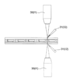
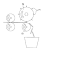
- FIG. 3 is an enlarged view of the cutting process I, and the cutting is performed by irradiating the infrared laser 30 and spraying water on the irradiation position with the water injection device 31. Then, it is cut into individual modules in a later process.
- FIG. 2 is a schematic diagram and shows a module that is separated into pieces instead of a fixed-size sheet.
- the cutting device composed of the infrared laser 30 and the water jet device 31 is configured to be movable integrally in a slightly oblique direction from the sheet width direction, and cuts the sheet while moving in this direction as the sheet is conveyed. Since the sheet is also moved, the sheet and the cutting device are relatively stationary by moving the infrared laser 30 and the water injection device 31 obliquely in the width direction. In addition, as shown by the arrow, the cutting device is configured to be movable in the contact / separation direction with respect to the sheet in order to adjust the focal position of the infrared laser.
- the back surface sealing sheet 3, the surface sealing sheet 4, and the spacer 6 are formed of an inorganic material, cracks generated in the surface sheet due to thermal expansion and contraction due to infrared laser irradiation and water cooling are also present in the spacer. Since it propagates and further propagates to the back sheet 3, laser cutting may be performed only from one side. However, when the spacer 6 is made of resin, the laser is emitted from both sides of the sheet as shown by dotted lines in FIG. Cutting may be performed.
- the sheet may be wound on a roll and separated into separate pieces, or further cut into both the width direction and the conveying direction to be separated into pieces.
- the individualized LED module 1 is completed through an electrode drawing process (not shown).
- the conductive ink is applied and dried on this portion, and the soldering surface is formed to complete the LED module 1.
- the cut LED modules 1 can be aligned in the same direction, and thus the electrode cut surfaces of a large number of LED modules can be formed.
- the conductive ink is applied together, dried and solidified as it is, and the electrode can be drawn out very efficiently.
- the number of electrodes is large, not two, the distance between the electrodes is short, so that a soldering portion for wiring can be formed by adhering metal leads with a conductive adhesive.
- Sheet material As a sheet material used for the front surface sealing sheet and the back surface sealing sheet, there are three types of materials, plastic, glass, and metal.
- Plastic materials include polyethylene, polycarbonate, cycloolefin, and acrylic.
- the thickness of the sheet material is about 1 ⁇ m to 1 mm. Since the optical semiconductor element module is formed in a matrix on the sheet material, the width is preferably about 300 mm, although it depends on the size of the optical semiconductor element module to be manufactured. If the width is too wide, the manufacturing equipment for maintaining high accuracy becomes expensive, and if the width is narrowed, the yield decreases.
- plastic sheet material is thin and excellent in heat dissipation, so it can be brighter than conventional plastic molding sealing, but many plastic materials themselves have heat resistance around 150 ° C and thermal conductivity Since it is low, it is not very suitable for high brightness applications. However, it is suitable for an inexpensive LED for display.
- the glass sheet As for the glass sheet, a sheet material having a thickness of 500 ⁇ m or less is already on the market in the form of a roll, and by using this, high heat resistance of the sheet can be secured and it can be used for high-luminance LED applications. Moreover, since this glass sheet is thin, the surface area per volume is large and the heat dissipation effect is large. Furthermore, if a material with high heat resistance such as low melting point glass is used for the spacer material, all materials constituting the LED module can be made of inorganic materials, so that the heat resistance is remarkably improved and not only suitable for high brightness applications. In the manufacturing process, since the drying / curing treatment can be performed at a high temperature of about 300 ° C., a highly reliable LED module can be manufactured.
- FIG. 4 shows the structure of the LED module 100 in this case. That is, the back surface sealing sheet 3 is a metal sheet, the p-side electrode 5p is formed on the metal sheet, and the insulating layer 10 is first formed on the n-side electrode 5n, and then the n-side electrode 5n is formed thereon. Is forming. Then, a separately manufactured LED chip 2 is turned on.
- the spacers 6a and 6b, the front side sealing sheet 4, and the phosphor 7 are the same as those in FIG.
- the entire mounting surface of the LED chip is in contact with a metal excellent in heat conduction, so that heat generated by light emission can be efficiently diffused to the sheet, and the semiconductor chip itself is prevented from being heated to high temperature. It is the most suitable sheet material for the LED module of the application.
- the loading surface of the LED chip and the metal sheet are tightly bonded by a conductive adhesive and are electrically connected.
- magnesium oxide, barium sulfate, titanium dioxide, or the like can be used, and these exhibit a reflectance of 95 to 99% or more over almost the entire region of visible light.
- Good white material These powders are mixed into the sheet raw material, and a plastic white sheet can be produced by a method such as melt stretching by heating or volatile solidification from solvent melting. Similarly, in the case of a glass sheet, a white sheet can be generated by melt drawing.
- the reflectance is slightly low, around 90%, but a white raw material that is easily clouded and can be applied to the present invention is used. Obtainable.
- the white sheet In the white sheet, light is scattered and reflected in all directions regardless of the incident direction, but in the case of a metal sheet, it is reflected in the same reflection angle direction as the incident angle of light in the form of a mirror.
- the blue reflectance is as low as 60% or less, so a surface such as silver or tin is previously coated on the surface on which the white or blue LED chip is placed.
- the reflectance can be improved by replacing the white reflection instead of the mirror reflection by a method such as applying the above-described white material to the surface of the semiconductor chip stacking side, but the thermal conductivity is slightly deteriorated.
- the adhesion of the electrode to the binder resin material and spacer resin material is greatly increased. This is preferable because it can prevent the peeling and cracking of the joint due to solder reflow or aging, and can improve the manufacturing yield and the reliability of the completed LED module.
- the adhesion of the electrode to the resin material or spacer material is dramatically improved.
- the yield and the reliability of the completed LED module can be improved, which is preferable.
- the silane coupling agent may be difficult to adhere.
- the SiO 2 coat is applied in advance and then the treatment with the silane coupling agent is performed. Just do it.
- the electrode can be formed by sheet screen printing, intaglio printing, or flexographic printing technology in which conductive ink is copied from the relief printing.
- the electrode material is supplied from the outside of the roll plate, but rotary screen printing in which the electrode material is supplied from the inside of the roll plate can also be used. Since such roll screen printing can be continuously performed without intermittent driving such as stopping and re-driving of sheets, an equipment such as an accumulator for taking the sheet feeding timing is unnecessary, and it is a simple and reliable process. So good.
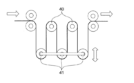
- the accumulator shown in FIG. 5 since intermittent driving such as stopping and re-driving of the sheet is required, the accumulator shown in FIG. 5 is used.
- the accumulator has a configuration in which a plurality of fixed rollers 40 and dance rollers 41 are alternately arranged, and a sheet material is alternately applied to each of the rollers. By moving the dance rollers 41, the speed on the carry-in side and the carry-out side can be increased. It can be changed or stopped. Since the electrode formation is the first step, this accumulator is arranged after the electrode formation step B, the driving of the supply roll is stopped, and the sheet is stopped. Then, an electrode is formed on the stationary sheet by sheet screen printing.
- the subsequent steps are transported at a constant speed, but the speed difference is absorbed by the accumulator. If it is desired to stop the sheet in the middle of the process, two accumulators may be provided, and a necessary process may be arranged between them.
- the electrode material conductive ink, conductive adhesive, or transparent conductive ink
- the electrode material conductive ink, conductive adhesive, or transparent conductive ink
- an electrode is previously formed on the sheet material, and the sheet with the electrode can be used in the manufacturing method of the present invention.
- the electrode forming step B in FIG. 2 can be omitted.
- Electrode material As the electrode material, conductive ink, conductive adhesive, and transparent conductive ink can be used, which will be described in order.
- the conductive ink contains silver particles and graphite as fillers.
- the thickness is 20 ⁇ m and the surface resistivity is 40 to 70 m ⁇ / cm 2.
- the heating condition is about 80 ° C. for about 30 minutes. For this reason, in the above-mentioned embodiment, it is not dried immediately after electrode printing, but is heated and dried in the first drying step E and the second drying step G.
- the binder of the conductive ink can have a relatively high viscosity when a UV curable resin is used, and the printing thickness can be reduced to about 10 to 20 ⁇ m.
- the viscosity of a binder such as a ketone or alcohol is low.
- the printing thickness is about half of about 6 to 10 ⁇ m.
- a weak ultraviolet light is irradiated to make the conductive ink in a semi-cured state. Send to process.
- Conductive adhesive Since the semiconductor chip and the electrode are directly joined in the post-process of electrode printing, the use of an ink imparted not only with conductivity but also adhesion may ensure more electrical joining.
- a conductive adhesive also uses silver particles as a filler, and one-component epoxy, phenol, polyimide, or the like is used as a resin binder.
- This conductive adhesive has a volume resistivity of 5 to 80 ⁇ 10 ⁇ 5 ⁇ ⁇ cm (approximately 0.05 to 0.8 ⁇ / cm 2 in terms of uniform surface resistivity) by heating and drying, and the conductivity of (1). The same resistance value as that of the conductive ink can be obtained.
- the drying and curing conditions are somewhat high, such as 150 ° C. for 30 minutes to 180 ° C. for 60 minutes (one component epoxy, phenol) and 290 ° C. for 20 minutes (polyimide).
- 150 ° C. for 30 minutes to 180 ° C. for 60 minutes one component epoxy, phenol
- 290 ° C. for 20 minutes polyimide
- Transparent conductive ink There are inks that are made transparent by using ITO fine particles, organic In-Sn, monodispersed Au-Ag, Ag nanoparticles, etc. as the filler of the conductive ink.
- the electrode can be generated by printing on the front side of the white sheet in the same manner as the conductive ink and the conductive adhesive.
- the LED light emitted to the white reflective sheet side was absorbed by the electrode, but it was transmitted by the transparent electrode and reached the white sheet, where high efficiency was achieved. After being reflected, the light passes through the transparent electrode and is returned to the LED chip, thereby contributing to an improvement in the intensity of the emitted light from the LED.
- This transparent conductive ink also needs to be dried by heating after printing. Temperature conditions of 120 ° C. are necessary for ITO fine particles, monodispersed Au—Ag and Ag nanoparticles, and 450 ° C. for organic In—Sn. Also, since the viscosity of the ink is generally low, the printed thickness is often thin, but the surface resistivity is slightly high at 0.05 to 2 ⁇ / cm 2 at a thickness of about 5 ⁇ m. By appropriately selecting the viscosity of the transparent conductive ink, it is possible to respond to commercially available products from low-viscosity ink printing such as gravure (intaglio printing) and inkjet printing, and high-viscosity screen printing.
- low-viscosity ink printing such as gravure (intaglio printing) and inkjet printing, and high-viscosity screen printing.
- the transparent conductive ink printed on the electrodes is semi-cured under a short heating condition for a short time and continuously sent to the next step.
- the LED module 110 When the electrode is arranged on the transparent sheet, that is, when the electrode is printed on the transparent sheet on the side where the LED light is emitted, a transparent conductive ink is used.
- the configuration of the LED module 110 in this case is shown in FIG.
- the LED module 110 first, the LED chip 2 is placed between the spacers 6a and 6b formed on the back surface sealing sheet 3, and the n-side electrode 5n and the p-side electrode 5p are made of transparent conductive ink thereon. Is formed by laminating and bonding the transparent front side sealing sheet 4. Alternatively, the n-side electrode 5n and the p-side electrode 5p may be formed on the transparent surface sealing sheet 4 in advance, and these may be laminated and bonded.
- the LED module 110 directly bonds the LED chip 2 to the electrodes 5n and 5p, there is no room for sandwiching the phosphor, and functions such as emission wavelength conversion using fluorescent light, increase in light quantity, and improvement in hue cannot be realized. This is for an LED module that emits the emission wavelength of the LED as it is.
- an offset gravure method is employed for the spacer forming step, but an inversion method in which printing is performed after removing an unnecessary spacer material in a semi-cured state with a relief printing plate may be used.
- a thick film can be formed relatively easily, so that it is more preferable for spacer printing.
- the creation of the spacer is also preferable because the spacer thickness can be increased by molding a UV curable resin or molding by thermal curing such as low melting point glass.
- Spacer material As the spacer material, a glass material such as gel glass or a low melting point glass paste, or an energy curable resin such as a thermosetting resin or a UV curable resin can be used.
- Low melting point glass paste uses frit glass (flakes or powdered glass blended with natural and industrial raw materials such as silica sand, feldspar, lime, etc., melted at high temperature, quenched and ground) Borosilicate glass or aluminosilicate glass that was made into a paste with water or solvent. A slightly softer slurry may be used. When this is continuously printed as an ink on a sheet and dried, it solidifies in a clay state and is sent to a subsequent process in this state.
- the glass is sintered into a dense glass body.
- the curing and sealing conditions are 400 to 450 ° C. for 10 minutes, and the sheet material is limited to glass or metal due to the high temperature, and the linear expansion coefficient is adjusted to prevent cracks due to differences in thermal expansion and contraction.
- the low-melting glass has a linear expansion coefficient ranging from 3 to 12 ppm, and can be selected as appropriate.
- Thermosetting resin or UV curable resin A spacer can also be continuously formed on a sheet with a thermosetting resin or a UV curable resin.
- a resin material bakelite, an epoxy resin, or an acrylic resin is usually used. However, since the heat resistance is 280 ° C. or higher, the resin material has reflow resistance and can withstand a drying / baking process below this temperature.
- the formed spacer is made into a semi-cured state and sent to the next step.
- the semi-cured state in the thermosetting resin, the curing heating conditions such as temperature and time are loosened, and in the UV curable resin, the UV is cured. This can be achieved by reducing the amount of irradiation.
- Complete curing is performed by heating or UV irradiation in a process after the mounting of the semiconductor chip or phosphor. This is because when the semiconductor chip and phosphor are mounted and sealed with a transparent sheet, if the spacer is pressed in a semi-cured state, the spacer material wets the transparent sheet and adhesion is increased. This is because the spacer is completely cured to improve hermeticity and certainty of sealing.
- the phosphor can be applied by a technique such as a droplet method in which a phosphor turbid liquid is dropped or an ink jet method. Also in this case, since the phosphor does not dissolve in the solvent, the solution is always put in a stirring state and applied while preventing precipitation or uneven distribution.
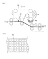
- FIG. 7 is a schematic view showing a modified example of the phosphor spray application.
- a mask for not applying the phosphor to unnecessary portions is made endless and continuously used and the phosphor is recovered.
- the mask 50 is formed in an endless belt shape using a stainless sheet or the like, and a plurality of openings are formed in a matrix shape in a portion where the phosphor is applied (see FIG. 7B).
- the spray 51 disposed inside the mask 50 may reciprocate in the width direction to apply the phosphor, or may be a line spray. After spray application, the mask 50 passes through a cleaning container 52 containing a solvent to wash off the phosphor, and then returns to the spraying process through a drying process by the infrared lamp 53.
- Phosphors have a very high specific gravity of about 3 to 5 and are insoluble in water, so the belt with the phosphors attached is peeled off and precipitated simply by soaking it in water or solvent. And can be reused. Since the phosphor is expensive, the phosphor can be applied at low cost by washing and collecting in this manner.
- the droplet method is a method in which a turbid liquid of phosphor is dropped at a desired position.
- a turbid liquid of phosphor is dropped at a desired position.
- the amount of the phosphor is adjusted by changing the size of the droplet depending on the outlet thickness of the syringe to be dropped and the number of drops.
- the glass sheet which is a transparent inorganic material is laminated and bonded, but a transparent plastic sheet can also be bonded by pressure bonding with a heating roller.
- sealing can be performed by applying a transparent plastic material or a transparent inorganic material.
- a transparent plastic material such as PET dissolved in methyl chloride or chloromethane.
- Application may be spray or roll printing, but the thickness of the plastic layer created by a single application is several ⁇ m, so repeated application and drying are repeated to increase the thickness of the plastic layer. Ensure sealing.
- PHPS all side chains are hydrogen
- the polysilazane) is dissolved in an organic solvent such as xylene and butyl ether. By containing an amine catalyst, it is dried and solidified even at room temperature to produce a dense glass layer of SiO 2 .
- a solvent containing moisture such as alcohol cannot be used.
- Such a polysilazane material can be sealed by being applied onto the LED chip on the sheet by spraying or coating, and then dried and cured. Furthermore, the phosphor is turbid in the polysilazane solvent, spray coated with a thickness of several tens of ⁇ m on the LED chip while stirring so as not to precipitate, and then dried and volatilized to form a dense glass seal containing the phosphor. Can do. That is, the phosphor coating process and the sealing process can be combined into one.
- the thickness of the glass generation layer by a single application of polysilazane is about several ⁇ m, and although it is a dense glass layer, its strength is weak and the sealing may be damaged. Repeated application and drying increase the thickness. And good. These multiple times of application
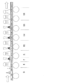
- FIG. 8 schematically shows a sealing process by polysilazane coating.
- the chip-on process D the first drying process E, the phosphor coating process F, and the second drying process G.
- three times of polysilazane spray coating are performed.
- drying by irradiation with an infrared lamp steps H1, H2, and H3.
- the irradiation light amount of the infrared lamp is adjusted so that the next coating step is started before the drying is completed. This is to avoid the occurrence of a clear boundary in the glass layer generated by coating, which causes cracks and peeling.
- the glass layer that has been laminated and applied is further integrated by heating to 200 to 250 ° C. with an infrared lamp (step H4) to further increase the denseness.
- the sealing process by the second sheet is not necessary, so the process is simplified, the equipment and the cover material are not required, the cost is low, and the yield can be improved. High quality LED products can be obtained stably.
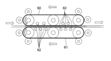
- the heating after sealing can be performed in a state of being sandwiched between endless belts 60 and 61 shown in FIG. 9 instead of a heating roller or an infrared lamp.
- Each of the two endless belts 60 and 61 is stretched around three rollers, and a pressing roller is disposed on the outer periphery of the belt.
- a plurality of heaters 62 are provided inside the endless belts 60 and 61, and the heat of the heaters 62 is applied to the sealed sheets via the endless belts 60 and 61. Since this heating method heats the sheet while pulling it straight, an optical semiconductor element module with high dimensional accuracy can be produced without bending.
- Cutting in the conveyance direction can be performed while carrying the infrared laser beam by the number of semiconductor modules arranged in the width direction, but cutting in the width direction requires maintaining the relative position of the laser cutting device and the sheet stationary. is there.
- the relative stationary method can be realized by the following two methods.
- A This is a method in which an accumulator is installed before the sheet feeding cutting process to allow extra time to wind up the sheet with a dance roller, and the sheet feeding in the laser cutting process is stopped during that time.
- the accumulator can have the above-described configuration.
- the laser cutting described above uses water for rapid cooling, so a drying process is required. By cutting the work directly into the pure water cleaning process after cutting, the drying process after cutting is unnecessary. Can do.
- the sheet on which the semiconductor chip is loaded uses a copper sheet to improve thermal conductivity, copper is difficult to cut with an infrared laser because of its high infrared reflectance, so an absorbent material is applied. It can be easy to keep.
- FIG. 10 schematically shows this cutting method.
- a band-shaped blade 71 is set on the drum surface of the rotary die 70, and the rotary die 70 and the bearer 72 are rotated in synchronization with sheet feeding. Cutting can be realized with an accurate dimension of the cut blade 70.
- the illustrated example is an example in which a blade is provided only in the width direction of the sheet.
- the semiconductor modules are cut into a line and separated into individual pieces.
- each semiconductor module can be separated into individual pieces. In this case, it is also necessary to have a configuration for winding the punched residue.
- the manufacturing method of the optical semiconductor element module of the present invention can greatly increase the production efficiency as compared with the conventional method.
- the number of LED modules that can be completed with one molding machine or sealing device is about 20 million pieces / year for resin sealing, and about 1/10 of that for glass sealing.
- the number of LED modules that can be manufactured by one unit per year is 7.29 billion / year. This calculation is based on a printing roll plate diameter of 120 mm, width of 300 mm, feed speed of 1 m / min, LED module size of 4 mm square, and device operation rate of 75%. Absent.
Landscapes
- Engineering & Computer Science (AREA)
- Manufacturing & Machinery (AREA)
- Led Device Packages (AREA)
Abstract
L'invention porte sur un procédé dans lequel une feuille, qui est formée avec une pluralité de modules d'élément à semi-conducteur optique, est préparée par l'exécution des étapes suivantes : une feuille continue, devant devenir un matériau d'étanchéité pour une surface, est transportée et, dans l'ordre du sens de transport de la feuille continue, des électrodes sont formées sur la feuille continue ; des puces d'élément à semi-conducteur optique préparées séparément sont montées entre des éléments intercalaires, et le matériau d'étanchéité de l'autre surface est amené et une étanchéité est obtenue.
Applications Claiming Priority (2)
| Application Number | Priority Date | Filing Date | Title |
|---|---|---|---|
| JP2010-041535 | 2010-02-26 | ||
| JP2010041535 | 2010-02-26 |
Publications (1)
| Publication Number | Publication Date |
|---|---|
| WO2011105185A1 true WO2011105185A1 (fr) | 2011-09-01 |
Family
ID=44506603
Family Applications (1)
| Application Number | Title | Priority Date | Filing Date |
|---|---|---|---|
| PCT/JP2011/052233 Ceased WO2011105185A1 (fr) | 2010-02-26 | 2011-02-03 | Procédé de fabrication de module d'élément à semi-conducteur optique |
Country Status (1)
| Country | Link |
|---|---|
| WO (1) | WO2011105185A1 (fr) |
Cited By (10)
| Publication number | Priority date | Publication date | Assignee | Title |
|---|---|---|---|---|
| WO2012090867A1 (fr) * | 2010-12-28 | 2012-07-05 | コニカミノルタオプト株式会社 | Procédé de fabrication d'un dispositif électroluminescent |
| WO2012152502A1 (fr) * | 2011-05-06 | 2012-11-15 | Osram Opto Semiconductors Gmbh | Composant optoélectronique à semi-conducteurs |
| JP2013168480A (ja) * | 2012-02-15 | 2013-08-29 | Konica Minolta Inc | Led装置の製造方法 |
| JP2017517833A (ja) * | 2014-03-20 | 2017-06-29 | イー・アイ・デュポン・ドウ・ヌムール・アンド・カンパニーE.I.Du Pont De Nemours And Company | 熱成形可能なポリマー厚膜透明導体および容量性スイッチ回路におけるその使用 |
| KR20180008712A (ko) * | 2015-08-18 | 2018-01-24 | 장쑤 체리티 옵트로닉스 컴퍼니, 리미티드 | 정제 광변환체로 led를 본딩 패키징하는 공정방법 및 정제 장비 시스템 |
| KR20180011159A (ko) * | 2015-08-18 | 2018-01-31 | 장쑤 체리티 옵트로닉스 컴퍼니, 리미티드 | 롤링 방식에 기반한 열가소성 수지 광 변환체로 led를 본딩 패키징하는 공정방법 |
| KR20180022862A (ko) * | 2015-08-18 | 2018-03-06 | 장쑤 체리티 옵트로닉스 컴퍼니, 리미티드 | 직렬 롤링에 기반한 유기 실리콘 수지 광 변환체로 led를 본딩 패키징하는 공정방법 |
| KR20180022861A (ko) * | 2015-08-18 | 2018-03-06 | 장쑤 체리티 옵트로닉스 컴퍼니, 리미티드 | 이형 유기 실리콘 수지 광변환체로 led를 본딩 패키징하는 장비 시스템 |
| KR20180022863A (ko) * | 2015-08-18 | 2018-03-06 | 장쑤 체리티 옵트로닉스 컴퍼니, 리미티드 | 직렬 롤링에 기반한 유기 실리콘 수지 광 변환체로 led를 본딩 패키징하는 장비 시스템 |
| KR20180022848A (ko) * | 2015-08-18 | 2018-03-06 | 장쑤 체리티 옵트로닉스 컴퍼니, 리미티드 | 롤링 방식에 기반한 열가소성 수지 광변환체로 led를 본딩 패키징하는 장비시스템 |
Citations (6)
| Publication number | Priority date | Publication date | Assignee | Title |
|---|---|---|---|---|
| JPH08184820A (ja) * | 1994-12-28 | 1996-07-16 | Sharp Corp | 機能膜付き基板の製造方法 |
| JP2007129188A (ja) * | 2005-10-07 | 2007-05-24 | Hitachi Maxell Ltd | 半導体装置、半導体モジュールおよび半導体モジュールの製造方法 |
| JP2008093662A (ja) * | 2007-11-05 | 2008-04-24 | Dainippon Screen Mfg Co Ltd | 塗布装置および塗布方法 |
| JP2008244357A (ja) * | 2007-03-28 | 2008-10-09 | Toshiba Corp | 半導体発光装置 |
| JP2009182149A (ja) * | 2008-01-30 | 2009-08-13 | Nitto Denko Corp | 光半導体素子封止用樹脂シートおよび光半導体装置 |
| JP2010021507A (ja) * | 2007-10-11 | 2010-01-28 | Hitachi Chem Co Ltd | 光半導体素子搭載用基板及びその製造方法、並びに光半導体装置及びその製造方法 |
-
2011
- 2011-02-03 WO PCT/JP2011/052233 patent/WO2011105185A1/fr not_active Ceased
Patent Citations (6)
| Publication number | Priority date | Publication date | Assignee | Title |
|---|---|---|---|---|
| JPH08184820A (ja) * | 1994-12-28 | 1996-07-16 | Sharp Corp | 機能膜付き基板の製造方法 |
| JP2007129188A (ja) * | 2005-10-07 | 2007-05-24 | Hitachi Maxell Ltd | 半導体装置、半導体モジュールおよび半導体モジュールの製造方法 |
| JP2008244357A (ja) * | 2007-03-28 | 2008-10-09 | Toshiba Corp | 半導体発光装置 |
| JP2010021507A (ja) * | 2007-10-11 | 2010-01-28 | Hitachi Chem Co Ltd | 光半導体素子搭載用基板及びその製造方法、並びに光半導体装置及びその製造方法 |
| JP2008093662A (ja) * | 2007-11-05 | 2008-04-24 | Dainippon Screen Mfg Co Ltd | 塗布装置および塗布方法 |
| JP2009182149A (ja) * | 2008-01-30 | 2009-08-13 | Nitto Denko Corp | 光半導体素子封止用樹脂シートおよび光半導体装置 |
Cited By (24)
| Publication number | Priority date | Publication date | Assignee | Title |
|---|---|---|---|---|
| WO2012090867A1 (fr) * | 2010-12-28 | 2012-07-05 | コニカミノルタオプト株式会社 | Procédé de fabrication d'un dispositif électroluminescent |
| WO2012152502A1 (fr) * | 2011-05-06 | 2012-11-15 | Osram Opto Semiconductors Gmbh | Composant optoélectronique à semi-conducteurs |
| US9142713B2 (en) | 2011-05-06 | 2015-09-22 | Osram Opto Semiconductors Gmbh | Optoelectronic semiconductor component |
| JP2013168480A (ja) * | 2012-02-15 | 2013-08-29 | Konica Minolta Inc | Led装置の製造方法 |
| JP2017517833A (ja) * | 2014-03-20 | 2017-06-29 | イー・アイ・デュポン・ドウ・ヌムール・アンド・カンパニーE.I.Du Pont De Nemours And Company | 熱成形可能なポリマー厚膜透明導体および容量性スイッチ回路におけるその使用 |
| EP3300127A4 (fr) * | 2015-08-18 | 2018-04-25 | Jiangsu Cherrity Optronics Co., Ltd | Procédé de traitement à l'aide d'un photoconvertisseur de résine thermoplastique pour encapsulation par liaison de del par laminage |
| EP3340320A4 (fr) * | 2015-08-18 | 2018-08-01 | Jiangsu Cherrity Optronics Co., Ltd | Procédé de traitement utilisant un photoconvertisseur en résine de silicone organique pour coller-encapsuler une del par cylindrage en tandem |
| KR20180022862A (ko) * | 2015-08-18 | 2018-03-06 | 장쑤 체리티 옵트로닉스 컴퍼니, 리미티드 | 직렬 롤링에 기반한 유기 실리콘 수지 광 변환체로 led를 본딩 패키징하는 공정방법 |
| KR20180022861A (ko) * | 2015-08-18 | 2018-03-06 | 장쑤 체리티 옵트로닉스 컴퍼니, 리미티드 | 이형 유기 실리콘 수지 광변환체로 led를 본딩 패키징하는 장비 시스템 |
| KR20180022863A (ko) * | 2015-08-18 | 2018-03-06 | 장쑤 체리티 옵트로닉스 컴퍼니, 리미티드 | 직렬 롤링에 기반한 유기 실리콘 수지 광 변환체로 led를 본딩 패키징하는 장비 시스템 |
| KR20180022848A (ko) * | 2015-08-18 | 2018-03-06 | 장쑤 체리티 옵트로닉스 컴퍼니, 리미티드 | 롤링 방식에 기반한 열가소성 수지 광변환체로 led를 본딩 패키징하는 장비시스템 |
| EP3300126A4 (fr) * | 2015-08-18 | 2018-04-25 | Jiangsu Cherrity Optronics Co., Ltd | Procédé de traitement d'affinement de photoconvertisseur pour coller-encapsuler une del, et système d'équipement d'affinement |
| KR20180008712A (ko) * | 2015-08-18 | 2018-01-24 | 장쑤 체리티 옵트로닉스 컴퍼니, 리미티드 | 정제 광변환체로 led를 본딩 패키징하는 공정방법 및 정제 장비 시스템 |
| EP3316320A4 (fr) * | 2015-08-18 | 2018-07-18 | Jiangsu Cherrity Optronics Co., Ltd | Système d'équipement utilisant un photo-convertisseur en résine de silicone organique pour coller-encapsuler une del par cylindrage en tandem |
| KR20180011159A (ko) * | 2015-08-18 | 2018-01-31 | 장쑤 체리티 옵트로닉스 컴퍼니, 리미티드 | 롤링 방식에 기반한 열가소성 수지 광 변환체로 led를 본딩 패키징하는 공정방법 |
| JP2018525816A (ja) * | 2015-08-18 | 2018-09-06 | ジアンスー チェリティ オプトロニクス カンパニー リミテッドJiangsu Cherrity Optronics Co., Ltd. | 直列ローリングによって有機シリコン樹脂光変換体でledを貼り合せてパッケージするプロセス方法 |
| JP2018527744A (ja) * | 2015-08-18 | 2018-09-20 | ジアンスー チェリティ オプトロニクス カンパニー リミテッドJiangsu Cherrity Optronics Co., Ltd. | 精製光変換体でledを貼り合せてパッケージするプロセス方法及び精製設備システム |
| JP2018527745A (ja) * | 2015-08-18 | 2018-09-20 | ジアンスー チェリティ オプトロニクス カンパニー リミテッドJiangsu Cherrity Optronics Co., Ltd. | 直列ローリングによって有機シリコン樹脂光変換体でledを貼り合せてパッケージする設備システム |
| KR101957870B1 (ko) | 2015-08-18 | 2019-03-13 | 장쑤 체리티 옵트로닉스 컴퍼니, 리미티드 | 롤링 방식에 기반한 열가소성 수지 광 변환체로 led를 본딩 패키징하는 공정방법 |
| KR101957871B1 (ko) | 2015-08-18 | 2019-03-13 | 장쑤 체리티 옵트로닉스 컴퍼니, 리미티드 | 정제 광변환체로 led를 본딩 패키징하는 공정방법 및 정제 장비 시스템 |
| KR101989042B1 (ko) | 2015-08-18 | 2019-06-13 | 장쑤 체리티 옵트로닉스 컴퍼니, 리미티드 | 롤링 방식에 기반한 열가소성 수지 광변환체로 led를 본딩 패키징하는 장비시스템 |
| KR101989043B1 (ko) | 2015-08-18 | 2019-06-13 | 장쑤 체리티 옵트로닉스 컴퍼니, 리미티드 | 이형 유기 실리콘 수지 광변환체로 led를 본딩 패키징하는 장비 시스템 |
| KR102026842B1 (ko) | 2015-08-18 | 2019-09-30 | 장쑤 체리티 옵트로닉스 컴퍼니, 리미티드 | 직렬 롤링에 기반한 유기 실리콘 수지 광 변환체로 led를 본딩 패키징하는 공정방법 |
| KR102026843B1 (ko) | 2015-08-18 | 2019-09-30 | 장쑤 체리티 옵트로닉스 컴퍼니, 리미티드 | 직렬 롤링에 기반한 유기 실리콘 수지 광 변환체로 led를 본딩 패키징하는 장비 시스템 |
Similar Documents
| Publication | Publication Date | Title |
|---|---|---|
| WO2011105185A1 (fr) | Procédé de fabrication de module d'élément à semi-conducteur optique | |
| TWI686965B (zh) | 發光裝置及其製造方法 | |
| JP5917739B2 (ja) | 蛍光体含有封止材の製造方法 | |
| JP5670051B2 (ja) | 半導体発光装置及びその製造方法 | |
| CN109155346A (zh) | 用于将磷光体施加至发光二极管的方法以及其设备 | |
| CN104201295A (zh) | Oled的封装方法及oled结构 | |
| CN114023777B (zh) | 电路板组件、发光组件及其制作方法 | |
| CN103456870B (zh) | 荧光粉胶涂覆的cob光源及其制造方法 | |
| CN111682094B (zh) | 一种led发光背板及其生产方法 | |
| KR20060095271A (ko) | 파장변환형 발광 다이오드 패키지 제조방법 | |
| KR101769356B1 (ko) | 발광소자에 형광체층을 형성하는 방법 및 장치 | |
| CN116741907A (zh) | 一种集成封装led显示模组及制备方法 | |
| CN113451491A (zh) | 显示面板及其制作方法 | |
| JP5375544B2 (ja) | 半導体発光装置及びその製造方法 | |
| JP2018523915A (ja) | ローリングによって熱可塑性樹脂光変換体でledを貼り合せてパッケージするプロセス方法 | |
| CN103165794A (zh) | 光学半导体装置用基台、其制造方法以及光学半导体装置 | |
| JP2004241695A (ja) | 光デバイスの製造方法 | |
| TWI620337B (zh) | 太陽電池模組的製造方法 | |
| JP6630373B2 (ja) | 不定形有機シリコン樹脂光変換体でledを貼り合せてパッケージするプロセス方法 | |
| JP2018530901A5 (fr) | ||
| JP2018525816A5 (fr) | ||
| KR20210101432A (ko) | 투명 led 디스플레이 모듈의 제조방법 | |
| JP2018525816A (ja) | 直列ローリングによって有機シリコン樹脂光変換体でledを貼り合せてパッケージするプロセス方法 | |
| KR101387847B1 (ko) | 롤러를 이용한 플렉서블 발광소자 전사방법, 제조방법 및 이에 의하여 제조된 플렉서블 발광소자 | |
| CN117594726A (zh) | 一种led封装器件的制备方法 |
Legal Events
| Date | Code | Title | Description |
|---|---|---|---|
| 121 | Ep: the epo has been informed by wipo that ep was designated in this application |
Ref document number: 11747149 Country of ref document: EP Kind code of ref document: A1 |
|
| NENP | Non-entry into the national phase |
Ref country code: DE |
|
| 122 | Ep: pct application non-entry in european phase |
Ref document number: 11747149 Country of ref document: EP Kind code of ref document: A1 |
|
| NENP | Non-entry into the national phase |
Ref country code: JP |