WO2011105434A1 - 半導体装置 - Google Patents
半導体装置 Download PDFInfo
- Publication number
- WO2011105434A1 WO2011105434A1 PCT/JP2011/054000 JP2011054000W WO2011105434A1 WO 2011105434 A1 WO2011105434 A1 WO 2011105434A1 JP 2011054000 W JP2011054000 W JP 2011054000W WO 2011105434 A1 WO2011105434 A1 WO 2011105434A1
- Authority
- WO
- WIPO (PCT)
- Prior art keywords
- junction
- layer
- semiconductor region
- junctions
- diode
- Prior art date
- Legal status (The legal status is an assumption and is not a legal conclusion. Google has not performed a legal analysis and makes no representation as to the accuracy of the status listed.)
- Ceased
Links
Images







Classifications
-
- H—ELECTRICITY
- H10—SEMICONDUCTOR DEVICES; ELECTRIC SOLID-STATE DEVICES NOT OTHERWISE PROVIDED FOR
- H10D—INORGANIC ELECTRIC SEMICONDUCTOR DEVICES
- H10D62/00—Semiconductor bodies, or regions thereof, of devices having potential barriers
- H10D62/10—Shapes, relative sizes or dispositions of the regions of the semiconductor bodies; Shapes of the semiconductor bodies
- H10D62/102—Constructional design considerations for preventing surface leakage or controlling electric field concentration
- H10D62/103—Constructional design considerations for preventing surface leakage or controlling electric field concentration for increasing or controlling the breakdown voltage of reverse-biased devices
- H10D62/105—Constructional design considerations for preventing surface leakage or controlling electric field concentration for increasing or controlling the breakdown voltage of reverse-biased devices by having particular doping profiles, shapes or arrangements of PN junctions; by having supplementary regions, e.g. junction termination extension [JTE]
-
- H—ELECTRICITY
- H10—SEMICONDUCTOR DEVICES; ELECTRIC SOLID-STATE DEVICES NOT OTHERWISE PROVIDED FOR
- H10D—INORGANIC ELECTRIC SEMICONDUCTOR DEVICES
- H10D62/00—Semiconductor bodies, or regions thereof, of devices having potential barriers
- H10D62/10—Shapes, relative sizes or dispositions of the regions of the semiconductor bodies; Shapes of the semiconductor bodies
- H10D62/102—Constructional design considerations for preventing surface leakage or controlling electric field concentration
- H10D62/103—Constructional design considerations for preventing surface leakage or controlling electric field concentration for increasing or controlling the breakdown voltage of reverse-biased devices
- H10D62/105—Constructional design considerations for preventing surface leakage or controlling electric field concentration for increasing or controlling the breakdown voltage of reverse-biased devices by having particular doping profiles, shapes or arrangements of PN junctions; by having supplementary regions, e.g. junction termination extension [JTE]
- H10D62/106—Constructional design considerations for preventing surface leakage or controlling electric field concentration for increasing or controlling the breakdown voltage of reverse-biased devices by having particular doping profiles, shapes or arrangements of PN junctions; by having supplementary regions, e.g. junction termination extension [JTE] having supplementary regions doped oppositely to or in rectifying contact with regions of the semiconductor bodies, e.g. guard rings with PN or Schottky junctions
-
- H—ELECTRICITY
- H10—SEMICONDUCTOR DEVICES; ELECTRIC SOLID-STATE DEVICES NOT OTHERWISE PROVIDED FOR
- H10D—INORGANIC ELECTRIC SEMICONDUCTOR DEVICES
- H10D62/00—Semiconductor bodies, or regions thereof, of devices having potential barriers
- H10D62/10—Shapes, relative sizes or dispositions of the regions of the semiconductor bodies; Shapes of the semiconductor bodies
- H10D62/102—Constructional design considerations for preventing surface leakage or controlling electric field concentration
- H10D62/112—Constructional design considerations for preventing surface leakage or controlling electric field concentration for preventing surface leakage due to surface inversion layers, e.g. by using channel stoppers
-
- H—ELECTRICITY
- H10—SEMICONDUCTOR DEVICES; ELECTRIC SOLID-STATE DEVICES NOT OTHERWISE PROVIDED FOR
- H10D—INORGANIC ELECTRIC SEMICONDUCTOR DEVICES
- H10D8/00—Diodes
- H10D8/411—PN diodes having planar bodies
-
- H—ELECTRICITY
- H10—SEMICONDUCTOR DEVICES; ELECTRIC SOLID-STATE DEVICES NOT OTHERWISE PROVIDED FOR
- H10D—INORGANIC ELECTRIC SEMICONDUCTOR DEVICES
- H10D8/00—Diodes
- H10D8/422—PN diodes having the PN junctions in mesas
-
- H—ELECTRICITY
- H10—SEMICONDUCTOR DEVICES; ELECTRIC SOLID-STATE DEVICES NOT OTHERWISE PROVIDED FOR
- H10D—INORGANIC ELECTRIC SEMICONDUCTOR DEVICES
- H10D8/00—Diodes
- H10D8/60—Schottky-barrier diodes
-
- H—ELECTRICITY
- H10—SEMICONDUCTOR DEVICES; ELECTRIC SOLID-STATE DEVICES NOT OTHERWISE PROVIDED FOR
- H10D—INORGANIC ELECTRIC SEMICONDUCTOR DEVICES
- H10D62/00—Semiconductor bodies, or regions thereof, of devices having potential barriers
- H10D62/80—Semiconductor bodies, or regions thereof, of devices having potential barriers characterised by the materials
- H10D62/83—Semiconductor bodies, or regions thereof, of devices having potential barriers characterised by the materials being Group IV materials, e.g. B-doped Si or undoped Ge
- H10D62/8303—Diamond
-
- H—ELECTRICITY
- H10—SEMICONDUCTOR DEVICES; ELECTRIC SOLID-STATE DEVICES NOT OTHERWISE PROVIDED FOR
- H10D—INORGANIC ELECTRIC SEMICONDUCTOR DEVICES
- H10D62/00—Semiconductor bodies, or regions thereof, of devices having potential barriers
- H10D62/80—Semiconductor bodies, or regions thereof, of devices having potential barriers characterised by the materials
- H10D62/83—Semiconductor bodies, or regions thereof, of devices having potential barriers characterised by the materials being Group IV materials, e.g. B-doped Si or undoped Ge
- H10D62/832—Semiconductor bodies, or regions thereof, of devices having potential barriers characterised by the materials being Group IV materials, e.g. B-doped Si or undoped Ge being Group IV materials comprising two or more elements, e.g. SiGe
- H10D62/8325—Silicon carbide
-
- H—ELECTRICITY
- H10—SEMICONDUCTOR DEVICES; ELECTRIC SOLID-STATE DEVICES NOT OTHERWISE PROVIDED FOR
- H10D—INORGANIC ELECTRIC SEMICONDUCTOR DEVICES
- H10D62/00—Semiconductor bodies, or regions thereof, of devices having potential barriers
- H10D62/80—Semiconductor bodies, or regions thereof, of devices having potential barriers characterised by the materials
- H10D62/85—Semiconductor bodies, or regions thereof, of devices having potential barriers characterised by the materials being Group III-V materials, e.g. GaAs
- H10D62/8503—Nitride Group III-V materials, e.g. AlN or GaN
Definitions
- the present invention relates to a semiconductor device.
- bipolar semiconductor elements such as pn junction diodes using silicon (Si) as a semiconductor material are used.
- Si silicon
- the injection of minority carriers causes conductivity modulation in the drift layer, resulting in significantly lower internal resistance. Because you can do it.
- the drift layer of the semiconductor element becomes thick and becomes high resistance. For this reason, it is preferable to use a pn junction diode capable of reducing the steady state loss.
- the diode having a built-in voltage lower than that of the pn junction diode means a Schottky junction diode or a p layer having an impurity concentration shallower and lower than that of the p layer constituting the pn junction diode (hereinafter referred to as a shallow pn layer) Shallow pn junction diode.
- a Si compound diode having an MPS (Merged Pin / Schottky) structure in which a pn junction and a Schottky junction are combined as shown in FIG. 18 or a pn junction and a shallow pn as shown in FIG.
- a soft and fast recovery diode (SFD) Si composite diode (SFD diode) in combination with a junction has been proposed and used.
- FIG. 18 is a cross-sectional view showing a conventional compound diode.
- the low breakdown voltage MPS diode shown in FIG. 18 is provided with an n ⁇ -type epitaxial layer to be an n ⁇ -drift layer 182 on the front surface side of the n + -type Si substrate 181.
- a pn junction surface and a Schottky junction surface are mixed.
- n - the surface layer of the drift layer 182 a plurality of p + -type region 183 is selectively provided, n - pn junction with the drift layer 182 and the p + -type region 183 is formed by repeatedly alternating It is formed.
- Schottky contact 184 is formed on the front surface side of Si substrate 181 and is in contact with p + -type region 183 and drift layer 182.
- the ohmic contact 185 is provided on the back surface of the Si substrate 181 and is in contact with the Si substrate 181.
- the outermost p + -type region 183 extends to a junction termination extension (JTE) region 190.
- the passivation film 191 is provided on the front surface side of the Si substrate 181 and covers a part of the p + -type region 183 of the termination portion and the n ⁇ drift layer 182 exposed in the junction termination structure region 190.
- the operation of the Schottky junction diode becomes dominant in the small current region and becomes a low forward voltage, while the operation of the pn junction diode becomes dominant in the large current region, and Schottky modulation is caused by conductivity modulation.
- the forward voltage is lower than that of the junction diode. For this reason, steady-state loss is reduced as compared in the entire current range.
- the MPS diode most of the accumulated carriers remaining in the drift layer when the switching operation is off are discharged through the Schottky junction, so that the annihilation time of the accumulated carriers can be shortened.
- the MPS diode is characterized in that the switching speed is high and the switching loss is also small (see, for example, Non-Patent Document 1 below).
- FIG. 19 is a cross-sectional view showing another example of a conventional compound diode.
- an n-type epitaxial layer to be an n-drift layer 202 is provided on the front surface side of the n + -type Si substrate 201.
- a pn junction surface and a shallow pn junction surface are mixed.
- the p + -type region 203 is selectively provided in the surface layer of the n-drift layer 202, and a pn junction composed of the n-drift layer 202 and the p + -type region 203 is formed.
- a shallow p type region 204 having an impurity concentration shallower and lower than that of the p + type region 203 is selectively provided.
- the shallow p-type region 204 is in contact with the p + -type region 203.
- the Schottky contact 205 is formed on the front surface side of the Si substrate 201 and is in contact with the p + -type region 203 and the shallow p-type region 204.
- the ohmic contact 206 is provided on the back surface of the Si substrate 201 and in contact with the Si substrate 201.
- the SFD diode has a breakdown voltage of, for example, 600V.
- the SFD diode is characterized by having a high switching speed and a small switching loss as compared to a pn junction only diode. Furthermore, SFD diodes can reduce reverse recovery current and can slow recovery time (soft recovery), and thus have the feature of being applied to inverters etc. and suppressing noise generation (see, for example, Non-Patent Document 2 below) ).
- SiC silicon carbide
- SiC silicon carbide
- SiC has an excellent characteristic that the dielectric breakdown electric field strength is about 10 times higher than that of Si, and realizes a high reverse voltage blocking characteristic.
- a pn junction diode which is a bipolar semiconductor device
- performance that is significantly superior to that of a pn junction diode using Si is realized.
- the reverse voltage is about 1/4 or less of the forward voltage and is equivalent to the speed at turn-off as compared to the pn junction diode using Si.
- the pn junction diode using SiC has high-speed switching operation, and can have a power loss of about 1/6 or less of that of the pn junction diode using Si. Therefore, wide gap semiconductor materials such as SiC are expected to greatly contribute to energy saving (see, for example, Non-Patent Document 3 below).
- the following device has been proposed as a semiconductor device using a wide gap semiconductor material.
- a junction between a drift layer and an anode layer of a bipolar semiconductor device and an electric field relaxation layer are formed separately from each other, and an end portion of an anode electrode is interposed between an insulating film and a semiconductor region between the junction and the electric field relaxation layer. Let them face each other.
- the junction and the field relaxation layer are electrically connected by the field effect given from the electrode to the drift layer between the junction and the field relaxation layer through the insulating film, and the field concentration at the end of the junction is relaxed.
- Ru At the time of forward bias, the junction and the electric field relaxation layer are also electrically separated to allow forward current to flow only through the junction (for example, see Patent Document 1 below).
- a semiconductor substrate having first and second surfaces, a first conductivity type cathode region adjacent to the first surface, and a first conductivity type drift region on the cathode region And a cathode electrode in contact with the cathode region, a second surface, and a first sidewall in the drift region, and a mesa formed between the first sidewall and the second sidewall.
- a second trench having a first sidewall, the first trench being provided and having the predetermined mesa width and the predetermined mesa doping concentration, and having the second sidewall portion in the second region and in the drift region.
- a first isolation region on the first sidewall and a second isolation region on the second sidewall, and over the second surface and the first and second isolation regions, also forms a Schottky rectifying junction with the mesa on the second surface That has an anode electrode, and further, the predetermined mesa doping concentration greater device than 1 ⁇ 10 16 dopant / cubic centimeter has been proposed (e.g., see below Patent Document 2.).
- JP 2005-223220 A Japanese Patent Publication No. 08-512430
- Non-Patent Documents 2 and 4 mentioned above do not mention the high breakdown voltage diode using the wide gap semiconductor material having the high breakdown voltage, and do not disclose the failure or the countermeasure associated with the high breakdown voltage. Furthermore, due to the limitations of the manufacturing process due to the difference between SiC used as a wide gap semiconductor material and Si, which is a conventional semiconductor material, and the limitations resulting from the processing accuracy of the current SiC processing process, the high performance of the original compound diode It is not mentioned that there are various problems in achieving gender. These problems are particularly serious problems in improving the performance of high performance high breakdown voltage compound diodes.
- pn junctions p + -type regions 183 and 203 constituting pn junctions (hereinafter referred to as pn main junctions) through which current flows. It is formed by ion implantation (ion implantation). However, many defects are generated in the pn junction formed in the SiC substrate by ion implantation.
- the impurity concentration needs to be increased in order to increase the carrier injection efficiency. Therefore, in the ion implantation for forming the p + -type regions 183 and 203, it is necessary to increase the dose amount, and the number of defects in the pn junction becomes extremely large. Due to this defect, a good Schottky junction or a shallow pn junction can not be formed in the vicinity of the contact portion between the pn main junction and the Schottky junction or the shallow pn junction, and withstand voltage characteristics in both forward and reverse directions are obtained. I lose it. In particular, in the case of a high breakdown voltage element in which the electric field applied to the Schottky junction or the shallow pn junction becomes high, the second problem occurs that the degradation of the above-described breakdown voltage is significantly generated.
- n - drift layer 182 constituting a Schottky junction provided in the vicinity of the front surface element surface and ap + -type region 203 (shallow pn junction) constituting a shallow pn junction
- This defect impairs the electrical characteristics in both forward and reverse directions.
- a high breakdown voltage element in which an electric field applied to a Schottky junction or a shallow pn junction becomes high, there is a third problem that the above-described deterioration of the breakdown voltage remarkably occurs.
- An object of the present invention is to provide a semiconductor device having a high withstand voltage in order to solve the above-mentioned problems of the prior art.
- An object of the present invention is to provide a semiconductor device capable of avoiding deterioration in withstand voltage characteristics.
- a semiconductor device comprises: a first semiconductor region of a first conductivity type made of a material having a wider band gap than silicon; A first layer selectively provided on the surface of the semiconductor region and forming a first junction with the first semiconductor region, and selectively provided on the surface of the first semiconductor region; A second layer forming a second junction with the first semiconductor region, a first diode including a region including the first junction, and a second including a region including the second junction A concave portion and a convex portion protruding from a bottom surface of the concave portion are provided on the surface of the first semiconductor region, and the first junction and the second junction are respectively Formed at different depths from the surface of the first semiconductor region Ri, built-in potential of the second diode is characterized by lower than built-in potential of the first diode.
- the first layer is provided on the surface of the convex portion
- the second layer is provided on the bottom surface of the concave portion.
- the depth from the surface of the convex portion of the first junction formed in the convex portion is shallower than the concave portion.
- an end portion of the first junction is exposed to a side surface of the convex portion.
- the semiconductor device according to the present invention is characterized in that, in the above-mentioned invention, the thickness of the second layer is smaller than that of the first layer.
- the first layer is a second semiconductor region of a second conductivity type
- the second layer is a third semiconductor region of the second conductivity type.
- the semiconductor region is characterized in that the third semiconductor region is thinner than the second semiconductor region and has an impurity concentration lower than that of the second semiconductor region.
- the second semiconductor region is an epitaxial layer selectively provided on the surface of the first semiconductor region, and the convex portion is the second semiconductor region. It is characterized in that it comprises two semiconductor regions.
- the semiconductor device according to the present invention is characterized in that, in the above-described invention, the first diode and the second diode are pn junction diodes.
- the first layer is a second semiconductor region of a second conductivity type
- the second layer is a portion of the second semiconductor region with the first semiconductor region. It is characterized in that it is a metal film forming a Schottky junction therebetween.
- the second semiconductor region is an epitaxial layer selectively provided on the surface of the first semiconductor region, and the convex portion is the second semiconductor region. It is characterized in that it comprises two semiconductor regions.
- the semiconductor device according to the present invention is characterized in that, in the above-mentioned invention, the first diode is a pn junction diode, and the second diode is a Schottky junction diode.
- the convex portion is provided in a tapered shape on a surface layer of the side surface of the concave portion between the first junction and the second junction.
- a fourth semiconductor region of a second conductivity type is provided in contact with the first junction and the second junction and having an impurity concentration lower than that of the second semiconductor region.
- the recess is a trench formed on the surface of the first semiconductor region on the side where the second semiconductor region is provided, Between the first junction and the second junction, and in contact with the first junction and the second junction and having a lower impurity concentration than the second semiconductor region on the surface layer of the sidewall of the trench A fourth semiconductor region of the second conductivity type is provided.
- a fifth semiconductor region of the second conductivity type having an impurity concentration lower than that of the second semiconductor region is provided on the surface layer of the bottom of the recess.
- the second junction provided on the bottom surface of the recess may be separated by the fifth semiconductor region.
- a semiconductor device is characterized in that, in the above-described invention, the third semiconductor region is a region formed by ion implantation.
- the metal film is an alloy layer formed by heat treatment after metal deposition.
- the first semiconductor region is provided on a semiconductor substrate of a first conductivity type made of a material having a wider band gap than silicon.
- a sixth semiconductor region which is thinner than the semiconductor substrate and has a high impurity concentration is provided in parallel to the surface of the semiconductor substrate, and the sixth semiconductor region is formed of the first semiconductor region. It is characterized in that it is provided closer to the semiconductor substrate than an intermediate depth inside the semiconductor region.
- the semiconductor device according to the present invention has a stripe planar layout in which the first junction and the second junction are alternately and repeatedly provided.
- the second junction and the second junction are arranged in the form of a stripe, and the end of the second junction is exposed at the outermost periphery in the direction orthogonal to the longitudinal direction of the stripe, and the second junction is parallel to the longitudinal direction of the stripe
- the end of the first junction and the end of the second junction are alternately exposed at the outermost periphery and provided at the outermost periphery, and the first junction and the second junction are provided.
- An electric field relaxation layer surrounding each of the first pn junction and the end of the second junction exposed to the outermost periphery.
- the MPS diode is manufactured using an epitaxial technique which can reduce defects remarkably as compared with the ion implantation technique. That is, ap + layer (second semiconductor region) is epitaxially grown on the n layer (first semiconductor region) to form a pn main junction (first junction), and the p + epitaxial layer is partially removed The Schottky junction (second junction) is formed on the n layer.
- the n layer is partially removed, the p + layer is epitaxially grown and embedded to form the pn main junction, and the Schottky on the unremoved n layer Forming a bond.
- an electric field relaxation region (JTE, FLR or RESURF) is formed on the n layer after removing the p + epitaxial layer, which contributes to realization of a high breakdown voltage.
- the p main junction and the Schottky junction are provided separately, and a p-fused field relaxation layer (fourth semiconductor region) having a concentration lower than that of the p + anode layer (second semiconductor region) is provided between both junctions. It is formed by implantation and contacts both junctions through this p-fused field relaxation layer.
- the fusion electric field relaxation layer is a fusion of the electric field relaxation layer of the pn main junction and the electric field relaxation layer of the Schottky junction, and has a function of achieving the electric field relaxation of both junctions simultaneously.
- the pn junction and the Schottky junction can be avoided, and only the p + anode layer can be provided at a high impurity concentration, while the p + anode layer is formed by ion implantation of the p impurity contacting the Schottky junction.
- the dose can be made smaller than that of the p + anode layer.
- the impurity concentration of the p-fused field relaxation layer is in the range of 5 ⁇ 10 15 cm -3 or more and 1 ⁇ 10 18 cm -3 or less in order to make the breakdown voltage of both the pn main junction and the Schottky junction high breakdown voltage. It is preferable that the range be 1 ⁇ 10 16 cm ⁇ 3 or more and 8 ⁇ 10 17 cm ⁇ 3 or less.
- the first problem solving means is used. That is, since the Schottky junction is formed at a lower position than the p + anode layer, mechanical stress directly extends on the top of the p + anode layer when wire bonding to the anode electrode, but It does not extend directly to bonding. Therefore, damage to the Schottky junction can be avoided. On the other hand, when the n layer is partially removed and the p + layer is epitaxially grown and embedded to form the pn main junction, the p + layer is made to be higher than the unremoved n layer. As a result, mechanical stress does not directly affect the Schottky junction during wire bonding, so damage to the Schottky junction can be avoided.
- the pn junction is formed in the lower part of the p + anode layer, that is, inside the SiC substrate (semiconductor substrate), mechanical stress at the time of wire bonding is considerably relieved. This can prevent the pn junction from being damaged. As a result, generation of defects at the time of wire bonding in both bonding portions can be suppressed, and favorable forward / reverse characteristics can be realized.
- p fusion electric field relaxation layer when the p + layer formed by epitaxial growth on the n layer partially removed by etching, the n-layer to form a p + layer in partially removing, the recess The corner portion of the metal is over-etched to frequently generate protruding grooves.
- the electric field is excessively concentrated on the over-etched protruding groove portion at the time of reverse bias, and the withstand voltage is lowered.
- the p-fused electric field alleviation layer described above also relieves the electric field concentration of the protruding grooves, so that this type of withstand voltage drop can be prevented and a high withstand voltage can be realized.
- the p + epitaxial layer is partially etched away to form the pn main junction, or when the n layer is partially removed to form the p + layer, the removed surface or the corner of the recess In the portion, various crystal defects resulting from etching are often formed.
- stacking faults have an adverse effect of capturing and annihilating carriers.
- the minority carriers injected from the pn main junction easily expand due to the impact when colliding with the crystal lattice of the stacking fault portion. As a result, the region for capturing and annihilating carriers is expanded, and the forward voltage is increased. Therefore, not only the steady state loss increases, but also the element may be broken.
- the p-fused field relaxation layer suppresses the collision of the injected carriers with the stacking fault near the etching surface and the corner surface, so that it is possible to suppress the increase of the steady loss and the element breakdown.
- one or more p layers (fifth semiconductor regions) having the above-described concentration range are provided in the Schottky junction.
- a reverse voltage equal to or higher than a predetermined reverse voltage an n layer sandwiched between p layers below the Schottky junction is pinched off by a depletion layer extending from the junction formed by both layers. It can be suppressed that the electric field strength of the Schottky junction is increased by the applied voltage.
- the entire width, that is, the area, of the Schottky junction is made approximately equal, an ultra-high breakdown voltage can be realized as compared to the conventional semiconductor device.
- the area of the Schottky junction can be expanded as compared with the conventional semiconductor device.
- the switching speed can be made faster, and as a result, the loss can be reduced.
- the ohmic contact metal film and the electrode film are formed in direct contact with the inclined surfaces on both sides of the convex portion where the p + anode layer is provided.
- the material of the ohmic contact film of the pn junction and the material of the Schottky junction metal are changed.
- the characteristics of the semiconductor device can be improved by using titanium (Ti) as the ohmic contact film of the p + layer and nickel (Ni) as the Schottky junction metal.
- the loss is reduced by providing a thick gold (Au) or aluminum (Al) film on the electrode film made of Ti and Ni and connecting the both while lowering the resistance of the anode electrode.
- an electric field relaxation region is formed such that both ends of the anode region in which pn main junctions and Schottky junctions are alternately arranged become Schottky junctions, and the Schottky junction end is provided on the n layer of the outer peripheral portion And contact with FLR or RESURF).
- both ends of the anode region is arranged to run in main pn junction, n under main pn junction across - the discharge time of the residual carriers in the drift layer is, n under other main pn junction inside - drift layer This is longer than the discharge time of the residual carrier inside, the reverse recovery time is longer, and the switching loss is higher.
- the semiconductor device with high withstand voltage can be provided.
- a wide gap MPS diode with few built-in defects can be provided, and high performance can be realized such as high withstand voltage, low loss, and high speed of the diode, and also reliability can be improved.
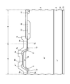
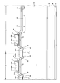
- FIG. 1 is a cross-sectional view showing the main parts of the MPS diode according to the first embodiment.
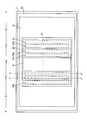
- FIG. 2 is a plan view showing the main part of the MPS diode according to the first embodiment.
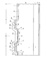
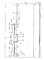
- FIG. 3 is a cross-sectional view showing the main parts of the MPS diode according to the second embodiment.
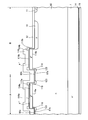
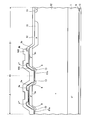
- FIG. 4 is a cross-sectional view showing the main parts of the MPS diode according to the third embodiment.
- FIG. 5 is a cross-sectional view showing the main parts of the MPS diode according to the fourth embodiment.
- FIG. 6 is a cross-sectional view showing the main parts of the MPS diode according to the fifth embodiment.
- FIG. 1 is a cross-sectional view showing the main parts of the MPS diode according to the first embodiment.
- FIG. 2 is a plan view showing the main part of the MPS diode according to the first embodiment.
- FIG. 3 is a cross-sectional view showing the main parts of the MPS di
- FIG. 7 is a cross-sectional view showing the main parts of the MPS diode according to the sixth embodiment.
- FIG. 8 is a cross-sectional view showing the main parts of a compound diode according to a seventh embodiment.
- FIG. 9 is a plan view showing the main part of a compound diode according to a seventh embodiment.
- FIG. 10 is a cross-sectional view showing the main parts of a compound diode according to an eighth embodiment.
- FIG. 11 is a cross-sectional view showing the main parts of a compound diode according to a ninth embodiment.
- FIG. 12 is a cross-sectional view showing the main parts of a compound diode according to a tenth embodiment.
- FIG. 13 is a cross-sectional view showing the main parts of a compound diode according to an eleventh embodiment.
- FIG. 14 is a cross-sectional view showing the main parts of a compound diode according to a twelfth embodiment.
- FIG. 15 is a cross-sectional view showing the main parts of a compound diode according to a thirteenth embodiment.
- FIG. 16 is a cross-sectional view showing the main parts of a compound diode according to a fourteenth embodiment.
- FIG. 17 is a cross-sectional view showing the main parts of a compound diode according to a fifteenth embodiment.
- FIG. 18 is a cross-sectional view showing a conventional compound diode.
- FIG. 19 is a cross-sectional view showing another example of a conventional compound diode.
- n and p in the layer or region having n or p, it is meant that electrons or holes are majority carriers, respectively.
- + and-attached to n and p mean that the impurity concentration is higher and the impurity concentration is lower than that of the layer or region to which it is not attached, respectively.
- FIG. 1 is a cross-sectional view showing the main parts of the MPS diode according to the first embodiment.
- the MPS diode shown in FIG. 1 is, for example, a high breakdown voltage wide gap semiconductor diode having a breakdown voltage of 16 kV class.
- an n ⁇ drift layer (first semiconductor region) 2 is provided on the front surface side of the n + cathode substrate 1.
- the n + cathode substrate 1 is made of, for example, a material (wide gap semiconductor) having a wider band gap than silicon, such as a four-layer periodic hexagonal crystal (4H—SiC) of silicon carbide.
- the impurity concentration and thickness of the n + cathode substrate 1 may be 2 ⁇ 10 19 cm ⁇ 3 and 400 ⁇ m, respectively.
- the impurity concentration and thickness of the n ⁇ drift layer 2 may be 4.5 ⁇ 10 14 cm ⁇ 3 and 170 ⁇ m, respectively.
- the n ⁇ drift layer 2 is formed by, for example, an epitaxial growth method.
- p + anode layers (first layer, second semiconductor region) 3a and 3b are provided separately from each other.
- a plurality of p + anode layers 3a are provided.
- the plurality of p + anode layers 3 a are provided to be separated from and adjacent to each other. Specifically, when the n + cathode substrate 1 is cut into individual chips, the p + anode layer 3 b is provided on the outer peripheral side of the chip, and the plurality of p + anode layers 3 a are more than the p + anode layer 3 b. It is provided on the center side of the chip (see FIG. 2).
- the impurity concentration and thickness of the p + anode layers 3a and 3b may be 5 ⁇ 10 18 cm ⁇ 3 and 1.7 ⁇ m, respectively.
- the p ++ contact layers 4a and 4b are provided on the surfaces of the p + anode layers 3a and 3b, respectively.
- the impurity concentration and thickness of the p ++ contact layers 4a and 4b may be 2 ⁇ 10 19 cm ⁇ 3 and 0.2 ⁇ m, respectively.
- the surface of the n - drift layer 2, p + anode layer 3a, 3b and the n - drift layer 2 which pn junction consisting of (pn main junction, the first junction) 5a, 5b are formed.
- a pn junction diode (first diode) including a region including the pn main junctions 5a and 5b is provided.
- the region including pn main junctions 5a and 5b is a region including at least n + cathode substrate 1, n ⁇ drift layer 2 and p + anode layers 3a and 3b.
- the p + anode layers 3a and 3b and the p ++ contact layers 4a and 4b are sequentially formed by epitaxial growth.
- the p + anode layers 3a and 3b and the p ++ contact layers 4a and 4b are processed into a mesa shape by RIE (Reactive Ion Etching) technology.
- RIE Reactive Ion Etching
- the height (hereinafter referred to as the height of the mesa) from the surface of the n ⁇ drift layer 2 exposed to the bottom surface of the mesa (hereinafter referred to as a recess to the bottom of the mesa) to the surface of the p ++ contact layers 4a and 4b is It may be about 2.5 ⁇ m.
- a Ti (second layer) film 6a is provided on the bottom of the mesa between adjacent p + anode layers 3a as a metal film for Schottky junction (hereinafter referred to as Schottky junction metal), and the Schottky junction (the 2) junction 7a is formed.
- a Ti (titanium) film 6b is provided as a Schottky junction metal to form a Schottky junction 7b. That is, a Schottky junction diode (second diode) formed of a region including the Schottky junctions 7a and 7b is provided.
- Schottky junction 7a a region containing 7b is at least n + cathode substrate 1
- n - is a region including the drift layer 2 and the Ti film 6a, a 6b.
- the built-in potential of the Schottky junction diode is lower than the built-in potential of the pn junction diode.
- the width C of the mesa bottom where the Schottky junctions 7a and 7b are formed may be about 40 ⁇ m.
- the distance D between the corner portion of the mesa bottom portion and the corner portion of the adjacent mesa bottom portion (hereinafter referred to as a convex portion between the mesa bottom portions) may be about 60 ⁇ m.
- Ti films 16a and 16b are provided on the p ++ contact layers 4a and 4b, respectively, as metal films (hereinafter referred to as ohmic contact metals) for ohmic connection of the anode.
- the Ti films 6a, 6b, 16a and 16b are formed by the same vapor deposition process and photolithography process.
- pn main junctions 5a and 5b and Schottky junctions 7a and 7b are formed as follows. First, the p + epitaxial layer and the p ++ epitaxial layer are sequentially stacked on the surface of the n ⁇ drift layer 2 stacked on the front surface of the n + cathode substrate 1. The p + epitaxial layer becomes p + anode layers 3a and 3b in a later step. The p ++ epitaxial layer becomes p ++ contact layers 4a and 4b in a later step.
- the p + epitaxial layer and the p ++ epitaxial layer stacked on the surface of the n ⁇ drift layer 2 are selectively etched and removed until the n ⁇ drift layer 2 is reached. At this time, part of the surface layer of the n ⁇ drift layer 2 may be removed together with the p + epitaxial layer and the p ++ epitaxial layer. Thereby, the mesa portion is formed.
- the p + epitaxial layer and the p ++ epitaxial layer are separated into a plurality of p + anode layers 3a and p ++ contact layers 4a, ap + anode layers 3b and p ++ contact layers 4b, and pn main junction 5a, 5b are formed.
- a Ti film is vapor-deposited on the entire front surface side of the n + cathode substrate 1. Then, the Ti film is selectively removed by photolithography to leave a Ti film laminated on the surface of the p ++ contact layers 4a and 4b and the bottom of the mesa. Thereby, Ti films 6a and 6b to be ohmic contacts are respectively formed on the surfaces of the p ++ contact layers 4a and 4b. In the bottom of the mesa, Ti films 16a and 16b are formed as a Schottky metal, and Schottky junctions 7a and 7b are formed. Through the above steps, pn main junctions 5a and 5b and Schottky junctions 7a and 7b are formed on the front surface side of n + cathode substrate 1 as follows.
- a recess is formed on the surface of n - drift layer 2 opposite to the surface in contact with n + cathode substrate 1, and then The p + epitaxial layer and the p ++ epitaxial layer may be grown in the recess, and the pn main junctions 5a and 5b may be formed on the bottom of the recess.
- Ti films 16a and 16b are formed as a Schottky metal on the surface of the n - drift layer 2 opposite to the surface in contact with the n + cathode substrate 1 and on which the recess is not formed.
- the junctions 7a, 7b are formed.
- p-fused electric field relaxation layer 13 In the surface layer of n - drift layer 2 exposed between pn main junction 5a and Schottky junction 7a and between pn main junctions 5a and 5b and Schottky junction 7b, p-fused electric field relaxation layer 13 ( The fourth semiconductor region is formed by ion implantation (ion implantation).
- the p-fused field relaxation layer 13 may be formed, for example, after removing the p + epitaxial layer and the p ++ epitaxial layer to form the p + anode layers 3a and 3b and the p ++ contact layers 4a and 4b.
- the impurity concentration and width of the p-fused field relaxation layer 13 may be about 8 ⁇ 10 16 cm ⁇ 3 and about 5 ⁇ m, respectively.
- the width of the p-fused field relaxation layer 13 is the length in the direction parallel to the front surface of the n + cathode substrate 1 from the end on the mesa bottom side.
- An anode electrode film 9 is formed on the front surface side of the n + cathode substrate 1 with an insulating protective film 8 provided on the side wall of the mesa portion.
- the anode electrode film 9 is in contact with the Ti films 6a, 6b, 16a and 16b.
- the anode electrode film 9 is made of, for example, Au (gold).
- the thickness of the anode electrode film 9 may be about 3.5 ⁇ m.
- the insulating protective film 8 provided on the side wall of the mesa portion is an end of the p + anode layers 3a and 3b exposed in the mesa, an end of the p ++ contact layers 4a and 4b, and a part of the p fused electric field relaxation layer Cover the
- a region from the central portion of the mesa portion to the central portion of the adjacent mesa portion is a composite unit A. That is, the composite unit A is composed of a region where the pn main junction 5a is formed and a region up to the central portion of the mesa formed on both sides of this region. A plurality of composite units A are arranged in parallel (see FIG. 2).
- the outermost peripheral area B is the region from the center of the mesa where the Schottky junction 7 b is formed to the outermost peripheral part of the chips. That is, the outermost peripheral portion B is a region including the pn main junction 5b formed on the outermost peripheral side of the chip.
- the p + epitaxial layer and p laminated on the surface of the n ⁇ drift layer 2 on the outer peripheral side of the chip than the region including the pn main junction 5 b are formed to form the p + anode layer 3 b and the p ++ contact layer 4 b
- the ++ epitaxial layer is removed along with the formation of the mesa, and the n ⁇ drift layer 2 is exposed.
- junction termination extension (JTE) 10 serving as an electric field relaxation region and a channel stopper 11 are formed by ion implantation in the surface layer of the n - drift layer 2 on the exposed surface.
- the JTE 10 and the channel stopper 11 are provided apart from each other.
- the JTE 10 and the channel stopper 11 surround a plurality of composite units A provided on the chip center side.
- the JTE 10 contacts the pn main junction 5 b formed on the outermost side.
- the JTE 10 and the channel stopper 11 are covered with a passivation film 12 formed by laminating a plurality of insulating films including an SiO 2 film.
- the passivation film 12 covers the end of the outermost exposed p + anode layer 3 b and the p ++ contact layer 4 b.
- the impurity concentration, width and depth of JTE 10 may be about 2.5 ⁇ 10 17 cm ⁇ 3 , 500 ⁇ m and 1.2 ⁇ m, respectively.
- the impurity concentration of the channel stopper 11 may be about 5 ⁇ 10 18 cm ⁇ 3 .
- a Ni ohmic contact 14 and a cathode electrode film 15 are formed on the back surface of the n + cathode substrate 1.
- the cathode electrode film 15 contains Au as a main component.
- FIG. 2 is a plan view showing the main part of the MPS diode according to the first embodiment.
- FIG. 2 shows a planar layout of a plurality of composite units A and an outermost peripheral portion B formed on a chip. Although the actual chip is square, the aspect ratio of the chip is about 1: 5 to clearly show the planar layout of the MPS diode.
- the Ti films 16a and 16b indicated by rough dotted rectangles and the Schottky junctions 7a and 7b indicated by solid rectangles constitute one unit 20, and for example, 30 units 20 are arranged adjacent to each other.
- a ⁇ n in the figure means that a plurality of units 20 are arranged.
- the Schottky junction 7b in the unit 20 includes the Ti film 16a in the unit 20 from the center of the Schottky junction 7a in one unit 20 and is adjacent to the Ti film 16a in the unit 20.
- the central portion is the combined unit A shown in FIG.
- the Schottky junction 7b in the unit 20 includes the Ti film 16b in the unit 20 and is adjacent to the Ti film 16a in the unit 20.
- the central portion may be a composite unit A.
- the composite unit A may be disposed so that the Ti film 16a and the Ti film 16b are alternately repeated in adjacent mesa portions.
- the outermost periphery B shown in FIG. 1 is from the central portion of the Schottky junction 7b in the unit 20 provided on the outermost side to the channel stopper 11 at the outermost periphery of the chip.
- the units 20 in the vicinity of the central portion of the chip are not shown and are indicated by thick and fine dotted lines.
- the length of the unit 20 in the direction in which the units 20 are arranged is, for example, 3 mm.
- JTE 10 encloses a complex unit group.
- the channel stopper 11 surrounds the JTE 10 and the composite unit group.
- the chip may be, for example, a square having a side of about 4 mm. That constitutes the direction orthogonal to the direction in which the unit 20 is arranged, Ti film 16a in the unit 20, pn junction 5a in (upper and lower ends of the cutting line E-E ') end of 16b, and 5b n -
- the drift layer 2 and the p + anode layers 3a and 3b are exposed, and the pn junctions 5a and 5b (see FIG. 1) are connected to the JTE 10.
- the Schottky junctions 7a and 7b are connected to the JTE 10 It is.
- Schottky junctions 7a and 7b can be formed deeper than pn main junctions 5a and 5b, when switching operation is off, n - drift layer 2 immediately below pn main junctions 5a and 5b is formed. It is easy to shorten the distance to the accumulated carrier remaining in the As a result, since accumulated carriers can be discharged more quickly and efficiently via Schottky junctions 7a and 7b having a built-in voltage lower than that of pn main junctions 5a and 5b, accumulated carrier annihilation time can be shortened and switching speed is fast. The reverse recovery current can be reduced.
- Example 1 Next, the operation and typical characteristics of the MPS diode according to the first embodiment will be described along with the operation at the time of the operation test of the MPS diode according to the first embodiment manufactured as the first embodiment.
- An MPS diode according to Example 1 was fabricated and mounted as follows. First, die bonding was performed to a TO type (pin insertion type) package. Then, a plurality of Au wires for wire connection were wire-bonded onto the anode electrode film 9 made of Au. The diameter of the Au wire was 100 ⁇ m. Then, the entire chip and most of the Au wire were coated with nanotech resin which is a high heat resistant resin for diode protection to fabricate a semiconductor device. And the operation test of the MPS diode concerning Example 1 was implemented.
- the potential of the anode electrode film 9 is higher than the potential of the cathode electrode film 15 between the anode electrode film 9 and the cathode electrode film 15, ie, so-called forward state Voltage was applied to the
- forward current started to flow from around 0.6 to 0.7V. This is because the Schottky junctions 7a and 7b are forward biased.
- the forward current started to rapidly increase from around 2.7 V. This is because the pn main junctions 5a and 5b are forward-biased and minority carrier injection is started, whereby the n - drift layer 2 is subjected to conductivity modulation to reduce the internal resistance.
- the MPS diode according to Example 1 had an average forward current density of about 40 A / cm 2 at a forward voltage of 5 V at room temperature, and was similar to a 5 kV class Si diode despite the high withstand voltage. From this, it was found that the MPS diode according to Example 1 had electrical characteristics sufficient for practical use as in the conventional Si diode, and could have a higher withstand voltage than the conventional Si diode. .
- the potential of the anode electrode film 9 is lower than the potential of the cathode electrode film 15 between the anode electrode film 9 and the cathode electrode film 15, ie, in the reverse direction.
- Voltage was applied. Leakage current tends to increase as the applied voltage increases.
- the breakdown current density of the leak current is 3 ⁇ 10 ⁇ 3 A / cm 2 or less at room temperature and 4 ⁇ 10 ⁇ 2 at a high temperature of 250 ° C. even when the applied voltage is 16 kV. The value was as low as A / cm 2 or less, showing good electrical characteristics.
- the withstand voltage which shows an avalanche breakdown became 18 kV or more at room temperature, and showed the favorable electrical property.
- a semiconductor device in which the p fused electric field relaxation layer 13 is not provided between the pn main junctions 5a and 5b and the Schottky junctions 7a and 7b is manufactured (hereinafter referred to as a first comparative example).
- the same operation test as the MPS diode was performed.
- the other configuration of the first comparative example is similar to that of the MPS diode according to the first embodiment.
- the forward breakdown voltage was about 5.2 kV.
- a Schottky junction is separated from the corner portion of the mesa bottom to manufacture a semiconductor device provided with only a guard ring (hereinafter referred to as a second comparative example).
- the same operation test as this MPS diode was conducted.
- the other configuration of the second comparative example is similar to that of the MPS diode according to the first embodiment.
- the forward breakdown voltage was about 6.8 kV.
- the MPS diode according to Example 1 had a reverse recovery time of 26 ns when it was turned off after passing a forward current at a forward current density of about 40 A / cm 2 .
- the reverse recovery current density was as low as about 54 A / cm 2 and that the electrical characteristics were very good.
- the test condition at this time is room temperature, the reverse applied voltage is 6.5 kV, and the reduction rate dj / dt of the current density is 7 kA / cm 2 / ⁇ s.
- pn diodes (only the third comparative example hereinafter) of pn main junctions 5a and 5b are fabricated without forming the Schottky junctions 7a and 7b, under the same conditions as the MPS diode according to the first embodiment.
- Reverse recovery time and reverse recovery current density were measured.
- the other configuration of the third comparative example is similar to that of the MPS diode according to the first embodiment.
- the reverse recovery time of the third comparative example was 57 ns.
- the reverse recovery current density of the third comparative example was about 165 A / cm 2 , which was higher than that of the MPS diode according to the first example. From this, it was found that the MPS diode according to the example 1 can reduce the leakage current more than the third comparative example.
- the width C of the mesa bottom where the Schottky junctions 7a and 7b are formed is 40 ⁇ m, and the distance D between the mesa bottoms is 60 ⁇ m.
- the width C of the mesa bottom and the distance D between the mesa bottoms may be variously changed without changing the total width (C + D) of the width C of the mesa bottom and the distance D between the bottoms. This makes it possible to change the trade-off relationship between the on voltage and the reverse recovery time.
- the on-voltage is increased by increasing the width C of the mesa bottom where the Schottky junctions 7a and 7b are formed, and reducing the distance D between the mesa bottoms where the pn main junctions 5a and 5b are formed.
- the reverse recovery time can be shortened.
- the width C of the bottom of the mesa and increasing the distance D between the bottoms of the mesa the reverse recovery time becomes longer, but the on-voltage can be reduced.
- the width C of the mesa bottom is 60 ⁇ m
- the distance D between the mesa bottoms is 40 ⁇ m
- the current flows at room temperature with a forward current density of about 40 A / cm 2
- the on voltage increases to 5.6 V.
- the time could be reduced to 19 ns.
- the MPS diode according to Example 1 was subjected to a reverse voltage application test with an applied voltage of 16 kV at a high temperature of 200 ° C. and a conduction test with a forward current density of 40 A / cm 2 for about 1000 hours.
- a reverse voltage application test with an applied voltage of 16 kV at a high temperature of 200 ° C.
- a conduction test with a forward current density of 40 A / cm 2 for about 1000 hours.
- the increase of the forward voltage due to the stacking fault tends to be reduced when the temperature of the diode is raised and reproduced when the temperature of the diode is returned to the original temperature.
- the reverse voltage application test and the current application test such an increase in forward voltage was not observed regardless of the temperature condition.
- a pn main junction 5a, 5b consisting of a layer is formed. Therefore, pn main junctions 5a and 5b can be formed in the SiC substrate without using ion implantation.
- no defect is generated in the p + anode layers 3a and 3b by ion implantation. Therefore, it is possible to avoid the occurrence of the leak current due to the defect formed in the p + anode layers 3a and 3b by the ion implantation. Therefore, it is possible to provide an MPS diode with high withstand voltage.
- the p + -anode layers 3a and 3b are processed into a mesa shape to form pn main junctions 5a and 5b, and Schottky junctions 7a and 7b are formed at the bottom of the mesa.
- pn main junctions 5a and 5b and Schottky junctions 7a and 7b do not come in contact with each other. Therefore, even if the impurity concentration of p + anode layers 3a and 3b functioning as the anode is increased in order to increase carrier injection efficiency, good Schottky junctions 7a and 7b with less leakage current can be formed. . Thereby, the leak current can be reduced, and deterioration of the breakdown voltage characteristics in both the forward direction and the reverse direction can be avoided.
- pn main junctions 5a and 5b are formed on the lower side of p + anode layers 3a and 3b. Therefore, the stress applied to the pn junction is relaxed by the thickness of the p + anode layers 3a and 3b. Thereby, damage to the pn junction can be reduced. Further, by forming the Schottky junctions 7a and 7b at the bottom of the mesa, an external force applied to the anode electrode film 9 at the time of wire bonding does not act on the Schottky junction. Thereby, damage to the Schottky junction can be avoided. Therefore, the occurrence of defects in the pn junction portion and the Schottky junction portion can be reduced, so that the leak current can be reduced, and deterioration of the breakdown voltage characteristics in both forward and reverse directions can be avoided.
- FIG. 3 is a cross-sectional view showing the main parts of the MPS diode according to the second embodiment.
- the MPS diode shown in FIG. 3 is, for example, a high voltage MPS diode having a withstand voltage of 13 kV.
- the MPS diode according to the second embodiment has a configuration different from the MPS diode according to the first embodiment in the following two points.
- the width of the Schottky junction formed at the bottom of the mesa between pn main junctions 35a and the width of the Schottky junction formed at the bottom of the mesa between pn main junction 35a and pn main junction 35b The width C is made wider than the Schottky junctions 7a and 7b of the first embodiment.
- a pinch-off p layer 30 (fifth semiconductor region) is provided in the central portion of the Schottky junction.
- the JTE 10 which is an electric field relaxation region is formed in the same ion implantation step as the p-fused electric field relaxation layer 13 to simplify the manufacturing process of the semiconductor device (not shown).
- the impurity concentration of the pinch-off p layer 30 is preferably lower than the impurity concentration of the p + -type region (see FIG. 18) constituting the pn junction of the conventional MSP diode.
- the reason is as follows.
- the pinch-off p-layer 30 mainly functions as an area for realizing pinch-off, and the function as an anode for injecting carriers is reduced. Then, the dose amount of ion implantation for forming the pinch-off p layer 30 can be reduced, and the generation of defects due to the ion implantation can be reduced. This is because generation of a leak current can be suppressed.
- the impurity concentration of the pinch-off p layer 30 may be about 2 ⁇ 10 17 cm ⁇ 3 .
- the pinch-off p layer 30 is formed in the same ion implantation step as the p-fused field relaxation layer 13. That is, as shown in the above (2), the JTE 10, the p-fused field relaxation layer 13 and the pinch-off p layer 30 are formed in the same ion implantation step.
- the Schottky junction formed at the bottom of the mesa between pn main junction 35a and pn main junction 35b by pinch-off p layer 30 is divided into Schottky junction 37b and Schottky junction 37c.
- the Schottky junction formed at the bottom of the mesa between the pn main junctions 35a is also divided into a Schottky junction 37a and a Schottky junction (not shown) by the pinch-off p layer 30.
- the widths of the p + anode layers 33 a and 33 b and the p ++ contact layers 34 a and 34 b constituting the pn main junctions 35 a and 35 b and the Ti films 36 a and 36 b as ohmic contact metals of the anode are the same as the p + anode of the first embodiment. It becomes narrower than the layers 3a and 3b, the p ++ contact layers 4a and 4b, and the Ti films 16a and 16b.
- the other configuration is the same as that of the MPS diode (see FIG. 1) according to the first embodiment.
- the switching operation when the switching operation is off, accumulated carriers remaining in the n ⁇ drift layer 2 can be discharged by the Schottky junctions 37 a, 37 b and 37 c wider than in the first embodiment. Therefore, the annihilation time of accumulated carriers can be further shortened. As a result, the switching speed can be made faster and the switching loss can be made smaller.
- Example 2 As Example 2, the MPS diode according to Embodiment 2 was manufactured.
- the MPS diode according to the second embodiment is provided with, for example, Schottky junctions 37 a, 37 b and 37 c divided by the pinch-off p layer 30.
- the distance from the end of the p-fused field relaxation layer 13 on the Ti film 36 a side to the end of the p-layer 30 for pinching off and the edge of the p-fused field relaxing layer 13 on the Ti film 36 b side The distance to each end was 20 ⁇ m.
- the width of the pinch-off p layer 30 is 5 ⁇ m.
- the impurity concentration of the pinch-off p layer 30 is about 2 ⁇ 10 17 cm ⁇ 3 .
- the other configuration is the same as that of the MPS diode according to the first embodiment.
- first to third comparative examples similar to the MPS diode according to example 1 were manufactured.
- the impurity concentration, width and depth of JTE 10 to be an electric field relaxation region were 3 ⁇ 10 17 cm ⁇ 3 , 350 ⁇ m and about 0.65 ⁇ m, respectively.
- the reverse applied voltage at a leak current density of 2 ⁇ 10 ⁇ 3 A / cm 2 was 13.6 kV at room temperature, and a higher withstand voltage could be realized compared to the first and second comparative examples.
- the MPS diode according to the second embodiment has a reverse recovery time of 14 ns when switched from the state where the forward current flows at a forward current density of about 40 A / cm 2 to the off state, and the switching operation is higher than that of the third comparative example. I was able to make it faster. Also, the reverse recovery current density was about 97 A / cm 2 , and the switching loss was almost the same as the MPS diode according to Example 1. The test conditions at this time are the same as those of the MPS diode according to the first embodiment.
- the corner portion of the mesa bottom portion of the portion (mesa portion) from which the p + epitaxial layer is removed in one wafer is over-etched due to the variation of the RIE etching conditions.
- a wafer in which a large number of grooves were formed was found.
- about 1/4 of each wafer does not form the p-fused field relaxation layer 13 for comparison experiments.
- the depth of the over-etched protrusion-like groove is about 0.4 ⁇ m at maximum, and there is concern that the electric field is excessively concentrated in this groove portion to lower the withstand voltage.
- the breakdown voltage is naturally low because the p fused electric field relaxation layer 13 is not present.
- the first comparative example having a low withstand voltage whose withstand voltage is significantly lower than the average withstand voltage of the first comparative example. did.
- part of the anode electrode film embedded in the mesa portion of the first comparative example with low withstand voltage (for example, about half in the direction perpendicular to the direction in which the composite units are arranged) is etched away and the remaining anode electrode is The corner portion of the bottom of the mesa was observed by a photo emission microscope in a state where a reverse voltage was applied to the film.
- a photo emission microscope in a state where a reverse voltage was applied to the film.
- specific light emission was observed at a relatively low reverse voltage in the groove at the corner of the bottom of the mesa in the anode electrode film removal portion. That is, it is suggested that the groove at the corner portion of the mesa bottom is the cause of the decrease in withstand voltage.
- the diode in which the p-fused field relaxation layer 13 was formed for example, the MPS diode according to the first and second embodiments
- no significant breakdown voltage element was found. It is presumed that the reason is that the high voltage resistance can be realized by the p-fused field relaxation layer 13 relaxing the electric field concentration in the protruding groove and preventing the decrease in the pressure resistance.
- FIG. 4 is a cross-sectional view showing the main parts of the MPS diode according to the third embodiment.
- the MPS diode shown in FIG. 4 is, for example, a high voltage MPS diode having a withstand voltage of 13 kV.
- the insulating protective film may not be provided.
- one Ti film may be provided to cover almost the entire surface of the front surface side of the n + cathode substrate 1.
- the insulating protective film is not provided on the side wall of the mesa portion on both sides of the p + anode layers 3a and 3b and the p ++ contact layers 4a and 4b.
- one Ti film 46 is provided on the front surface side of the n + cathode substrate 1. The Ti film 46 is in contact with the p ++ contact layers 4 a and 4 b and the n ⁇ drift layer 2 exposed at the bottom of the mesa. Further, an anode electrode film 49 covering the Ti film 46 is provided on the Ti film 46.
- the other configuration is the same as that of the first embodiment.
- the lift-off process at the time of forming the Ti films 6a, 6b, 16a and 16b in the first embodiment can be omitted.
- the manufacturing process of the semiconductor device can be simplified, and the yield of the semiconductor device can be greatly improved, so that the cost can be reduced.
- the anode electrode film 49 made of Au contacts the p-fused field relaxation layer 43 via the Ti film 46. Therefore, when a high reverse voltage is applied, the p-fused field relaxation layer 43 is punched through. In order to prevent this, it is preferable to set the thickness of the p-fused field relaxation layer 43 to, for example, 1.2 ⁇ m, and to be thicker than the first embodiment. Furthermore, the impurity concentration of the p-fused field relaxation layer 43 is preferably 3.5 ⁇ 10 17 cm ⁇ 3 , for example, and preferably higher than that of the first embodiment.
- Example 3 As Example 3, an MPS diode according to Embodiment 3 was produced. Specifically, the MPS diode according to the third embodiment does not have the insulating protective film on the side wall of the mesa portion on both sides of the p + anode layers 3a and 3b and the p ++ contact layers 4a and 4b. Further, a Ti film 46 continuously extending from the p ++ contact layer 4 b to the mesa bottom and the p ++ contact layer 4 a is provided. The thickness and impurity concentration of the p-fused field relaxation layer 43 were 1.2 ⁇ m and 3.5 ⁇ 10 17 cm ⁇ 3 , respectively. The other configuration is the same as that of the MPS diode according to the first embodiment.
- the leakage current density slightly increased to 6 ⁇ 10 ⁇ 3 A / cm 2 when a reverse voltage of 16 kV was applied at room temperature, but the breakdown voltage showing avalanche breakdown was 18 kV or more at room temperature.
- the same result as the MPS diode according to Example 1 was obtained.
- the MPS diode according to Example 3 slightly increased the function as an anode for injecting carriers when a forward voltage was applied, and the on voltage decreased.
- the on voltage was 4.85 V when the forward voltage at a forward current density of about 40 A / cm 2 was at room temperature.
- FIG. 5 is a cross-sectional view showing the main parts of the MPS diode according to the fourth embodiment.
- the MPS diode shown in FIG. 5 is, for example, a high voltage MPS diode having a withstand voltage of 16 kV.
- a Ni film is provided instead of the Ti film of the MPS diode according to the third embodiment.
- a Ti film for ohmic contact may be provided between the p ++ contact layers 4a and 4b and the Ni film.
- Ti films 56a and 56b are provided on the surfaces of the p ++ contact layers 4a and 4b, respectively.
- a Ni film 66 continuously extending from Ti films 56a and 56b provided on the p ++ contact layers 4a and 4b to the bottom of the mesa is provided. That is, Ti films 56a and 56b are provided as ohmic contact metals for pn junction, and Ni film 66 is provided as Schottky junction metal. In this case, after the Ti films 56a and 56b are formed, a Ni film 66 is separately formed.
- the other configuration is the same as that of the third embodiment.
- Example 4 As Example 4, the MPS diode according to Embodiment 4 was manufactured. Specifically, in the MPS diode according to the fourth embodiment, the Ti films 56a and 56b are formed as an ohmic contact metal, and the Ni film 66 is formed as a Schottky junction metal. The other configuration is the same as that of the MPS diode according to the third embodiment.
- the MPS diode according to the fourth embodiment after forming the Ti films 56a and 56b for ohmic contact, heat treatment is performed on the Ti films 56a and 56b before forming the Ni film 66 which is a Schottky junction metal. Therefore, the Ni film 66, which is a Schottky junction metal, is not affected by the heat treatment performed on the Ti films 56a and 56b. Therefore, the temperature of heat treatment performed on Ti films 56a and 56b can be set as high as 950 ° C., and an ohmic contact of good p ++ contact layers 4a and 4b with low contact resistance can be formed. As a result, the forward voltage of the MPS diode according to the fourth embodiment can be lowered by about 0.4 V, and the steady loss can be reduced.
- FIG. 6 is a cross-sectional view showing the main parts of the MPS diode according to the fifth embodiment.
- the MPS diode shown in FIG. 6 is, for example, a high voltage MPS diode having a withstand voltage of 20 kV class.
- the MPS diode according to the fifth embodiment includes an anode electrode film provided above the pn junctions 5a and 5b and an anode electrode film provided above the Schottky junctions 7a and 7b of the MPS diode according to the first embodiment. Are provided separately.
- anode electrode films 69c and 69d are in contact with Ti films 6a and 6b forming Schottky junctions 7a and 7b, respectively.
- Anode electrode films 69a and 69b are in contact with the Ti films 16a and 16b provided above the pn junctions 5a and 5b, respectively.
- the impurity concentration of the n ⁇ drift layer 62 is, for example, 3 ⁇ 10 14 cm ⁇ 3 , which is lower than that of the first embodiment.
- the thickness of the n ⁇ drift layer 62 is, for example, 220 ⁇ m, which is thicker than that of the first embodiment.
- the impurity concentration of the p-fused field relaxation layer 63 is higher than that of the first embodiment, for example, 3 ⁇ 10 17 cm ⁇ 3 .
- the other configuration is the same as that of the first embodiment.
- the anode electrode film is not present on the side wall of the mesa portion where the end of the p + anode layers 3a and 3b is exposed. Therefore, no carrier induction occurs on the side wall of the mesa portion due to the electric field effect of the anode electrode film when the reverse voltage is applied. Therefore, it is possible to realize a high breakdown voltage MPS diode that is stable and has less variation as compared to the first embodiment.
- the MPS diode according to the fifth embodiment has the following planar layout.
- the outer peripheral portion in the direction in which the units 20 are arrayed is a p in the unit 20 arrangement direction of the composite unit group consisting of 30 units 20 and one p + anode layer 3 b provided in parallel to the composite unit group + Surrounded by the JTE 10 in contact with the anode layer 3b.
- the outer peripheral part of the composite unit group consisting of 30 units 20 and one p + anode layer 3 b provided in parallel to the composite unit group in the direction orthogonal to the direction in which units 20 are arranged is a separate unit
- a p + layer (hereinafter referred to as a laterally long p + layer, not shown) extending in a direction in which 20 is arranged is provided in contact with the 31 p + anode layers 3a and 3b and the 30 Schottky junctions 7a and 7b ing.
- the outer peripheral portion of the horizontal p + layer is surrounded by a JTE10 contacting the horizontal p + layer.
- the channel stopper 11 surrounds the outer periphery of the JTE 10.
- An ohmic contact metal Ti film and an Au electrode are formed on the horizontal p + layer (not shown), and anode electrode films 69a, 69b and 69c provided above the respective p + anode layers 3a and 3b. , 69 d respectively.
- the laterally long p + layer functions as a p + anode layer.
- the laterally long p + layer, the Ti films 6a and 6b, which are Schottky metals, and the anode electrode films 69a, 69b, 69c, and 69d extend over the insulating protection film in contact with the end of the laterally long p + layer. It is connected to a Ti film or an Au electrode which is an ohmic contact metal on the + layer.
- Example 5 As Example 5, an MPS diode according to Embodiment 5 was produced. Specifically, in the MPS diode according to the fifth embodiment, the anode electrode films 69a, 69b, 69c, 69d are in contact with the Ti films 16a, 16b, 6a, 6b, respectively.
- the impurity concentration and thickness of n - drift layer 62 provided with laterally long p + layers in contact with Ti films 16a, 16b, 6a, 6b and anode electrode films 69a, 69b, 69c, 69d are respectively 3 ⁇ 10 It was 14 cm -3 and 220 ⁇ m.
- the impurity concentration of the p-fused field relaxation layer 63 is set to 3 ⁇ 10 17 cm ⁇ 3 .
- the other configuration is the same as that of the MPS diode according to the first embodiment.
- the breakdown voltage showing the avalanche breakdown is as high as 21 kV or more at room temperature, and the variation of the leak current can be reduced by about 40% as compared with the MPS diode according to the first embodiment.
- the influence of the electric field effect of the Ti film or the Au electrode portion which is an ohmic contact metal on the horizontally long p + layer is not a level which causes a problem in practical use because the area ratio is small.
- FIG. 7 is a cross-sectional view showing the main parts of the MPS diode according to the sixth embodiment.
- the MPS diode shown in FIG. 7 is, for example, a high voltage MPS diode having a withstand voltage of 16 kV class.
- the MPS diode according to the seventh embodiment does not have the pn main junction 5b at the outermost peripheral portion B of the MPS diode according to the first embodiment.
- the p + anode layer 3 b and the p ++ contact layer 4 b constituting the pn main junction 5 b are not provided in the outermost peripheral portion B.
- the end portions of the Ti film 6b constituting the Schottky junction 7b are overlapped and in contact with each other.
- the width of the overlapping portion may be, for example, about 3 ⁇ m.
- the width of the Schottky junction 7b is 40 ⁇ m as in the first embodiment.
- the other configuration is the same as that of the MPS diode according to the first embodiment.
- the width of the p + anode layer 3b of the outermost peripheral portion B is substantially the same as the width of the p + anode layer 3a of the composite unit A, the n ⁇ drift of the outermost peripheral portion B when the switching operation is off
- the discharge time of accumulated carriers in layer 2 was longer than the discharge time of accumulated carriers in n - drift layer 2 of composite unit A, and as a result, the reverse recovery time was increased.
- the reverse recovery time can be shortened by not providing the p + anode layer 3 b in the outermost peripheral part B.
- the reason is that, in the composite unit A according to the first embodiment, the remaining carriers are discharged from both sides by the Schottky junctions 7a and 7b formed on the mesa bottoms on both sides of the p + anode layer 3a. In part B, it is because it is discharged only from the side of one Schottky junction 7b.
- Example 6 As Example 6, an MPS diode according to Embodiment 6 was produced. Specifically, in the MPS diode according to the sixth embodiment, the p + anode layer 3 b is not provided at the outermost peripheral portion B. The other configuration is the same as that of the MPS diode according to the first embodiment. In the MPS diode according to the sixth embodiment, the discharge time is not uneven as in the MPS diode according to the first embodiment, and the reverse recovery time can be shortened.
- the reverse recovery time of the MPS diode according to the sixth embodiment was measured in the same manner as the MPS diode according to the first embodiment.
- the measurement conditions are the same as those of the MPS diode according to the first embodiment.
- the MPS diode according to Example 6 had a reverse recovery time of 21 ns, and could be reduced by about 20% compared to the MPS diode according to Example 1. As a result, the switching loss could also be reduced.
- the breakdown voltage of the MPS diode according to the sixth embodiment is 16.2 kV, which is slightly lower than that of the MPS diode according to the first embodiment. The reason is that the electric field concentration at the end of the anode electrode film 9 on the JTE 10 is high. In this case, the electric field concentration at the end of the anode electrode film 9 can be alleviated by further increasing the thickness of the passivation film 12 on the anode electrode film 9 side.
- FIG. 8 is a cross-sectional view showing the main parts of a compound diode according to a seventh embodiment.
- the compound diode shown in FIG. 8 is, for example, a high voltage compound diode having a withstand voltage of 16 kV class.
- the composite diode according to the seventh embodiment is shallower and lower than the p + anode layers 3a and 3b constituting the pn main junctions 5a and 5b instead of the Schottky junctions 7a and 7b of the MPS diode according to the first embodiment.
- a shallow pn junction formed of ap layer (shallow pn layer) having an impurity concentration may be used.
- the impurity concentration and thickness of n drift layer 82 are 4 ⁇ 10 14 cm ⁇ 3 and 170 ⁇ m, respectively.
- the Al / Si alloy electrode films 86a and 86b are formed at the bottom of the mesa.
- the Al / Si alloy electrode films 86a and 86b are formed by a lift-off method. In the lift-off method, the entire surface of the device is covered with a resist, and only the resist at the mesa bottom is etched away by photolithography and then an Al ⁇ Si alloy film is deposited to form an Al ⁇ Si alloy electrode film 86a, 86b only at the mesa bottom. Method to leave Thereafter, heat treatment at 700 ° C. or more and 1100 ° C.
- shallow pn junctions (second layer, third semiconductor region) 87a and 87b are formed in the surface layer at the bottom of the mesa.
- the impurity concentration and thickness of the shallow p layer forming the shallow pn junctions 87a and 87b may be, for example, 8 ⁇ 10 16 cm ⁇ 3 and about 20 nm, respectively.
- the width C of the mesa bottom where the shallow pn junctions 87a and 87b are formed may be 40 ⁇ m, and the distance D between the mesa bottoms may be 60 ⁇ m.
- Ti films 96a and 96b are formed as an ohmic contact metal using a lift-off method.
- An anode electrode film 89 made of Al is formed on the front surface side of the n + cathode substrate 1 through the insulating protective film 8 provided on the side wall of the mesa portion. The other conditions of the anode electrode film 89 are the same as those of the anode electrode film of the first embodiment.
- p fused electric field relaxation layer 13 is formed, respectively. It is done.
- the impurity concentration and width of the p-fused field relaxation layer 13 are about 1 ⁇ 10 17 cm ⁇ 3 and 4 ⁇ m, respectively.
- the width of the p-fused field relaxation layer 13 is the mesa bottom of the overlapping portion of the shallow pn junctions 87a and 87b and the p-fused field relaxation layer 13 in the mesa bottom from the exposed position on the mesa side wall of the pn main junctions 5a and 5b. It is the length from the corner to the longest end.
- the other configuration is the same as that of the first embodiment.
- FIG. 9 is a plan view showing the main part of a compound diode according to a seventh embodiment.
- the planar layout of the plurality of composite units A and the outermost peripheral portion B formed on the chip is the same as that of the first embodiment. That is, the shallow pn junctions 87a and 87b and the Ti films 96a and 96b in the unit 20 are arranged in the same manner as the Schottky junctions 7a and 7b and the Ti films 16a and 16b of the first embodiment shown in FIG.
- the shallow pn junctions 87a and 87b can be formed deeper than the pn main junctions 5a and 5b. Therefore, when the switching operation is off, the pn main junctions 5a and 5b are formed. It becomes easy to shorten the distance to the accumulated carriers remaining in the n drift layer 82 immediately below. As a result, since accumulated carriers can be discharged more quickly and efficiently via the shallow pn junctions 87a and 87b having a built-in voltage lower than that of the pn main junctions 5a and 5b, accumulated carrier annihilation time can be shortened and switching speed is fast. The reverse recovery current can be reduced.
- Example 7 As Example 7, a composite diode according to Embodiment 7 was produced. Specifically, the composite diode according to the seventh embodiment uses an Al wire instead of the Au wire of the MPS diode according to the first embodiment. In the composite diode according to the seventh embodiment, the anode electrode film 89 made of Al and the shallow pn junction 87a, made of Al instead of the anode electrode film 9 made of Au and the Schottky junctions 7a and 7b of the MPS diode according to the first embodiment. 87b is provided. The other configuration is the same as that of the MPS diode according to the first embodiment. And the operation test of the compound diode concerning Example 7 was implemented.
- the composite diode according to Example 7 had an average forward current density of about 45 A / cm 2 at a forward voltage of 5 V at room temperature and was equivalent to a 5 kV class Si diode despite the high withstand voltage. From this, it was found that the composite diode according to Example 7 had the same effect as the MPS diode according to Example 1.
- the breakdown current density of the leak current is 1.5 ⁇ 10 ⁇ 3 A / cm 2 or less at room temperature even when the applied voltage is 10 kV, and the applied voltage is 16 kV.
- the value was as low as 3 ⁇ 10 -3 A / cm 2 or less at room temperature, and 4 ⁇ 10 -2 A / cm 2 or less at a high temperature of 250 ° C., indicating excellent electrical characteristics.
- the withstand voltage which shows an avalanche breakdown became 18 kV or more at room temperature, and showed the favorable electrical property.
- the fourth comparative example a semiconductor device in which the p fused electric field relaxation layer 13 is not provided between the pn main junctions 5a and 5b and the shallow pn junctions 7a and 7b is fabricated (hereinafter referred to as the fourth comparative example).
- the same operation test as the compound diode was performed.
- the other configuration of the fourth comparative example is similar to that of the compound diode according to the seventh embodiment.
- the forward withstand voltage was about 5.2 kV.
- a semiconductor device is manufactured in which a guard ring is provided by separating the shallow pn junction from the corner portion of the mesa bottom instead of the p-fused field relaxation layer 13 (hereinafter referred to as the fifth comparative example).
- the same operation test as this composite diode was conducted.
- the other configuration of the second comparative example is similar to that of the composite diode according to the seventh embodiment.
- the forward breakdown voltage was about 6.8 kV. From this, it was found that the composite diode according to Example 7 had the same effect as the MPS diode according to Example 1.
- the reverse recovery time is 26 ns and the reverse recovery current density is about 34 A / when switching from the forward current flow state at a forward current density of about 50 A / cm 2 to the off state. It was found to be as low as cm 2 and to exhibit extremely good electrical characteristics.
- the test conditions at this time are the same as those of the MPS diode according to the first embodiment.
- a diode of pn junctions 5a and 5b alone (hereinafter referred to as a sixth comparative example) is fabricated without forming shallow pn junctions 87a and 87b, and reverse recovery is performed under the same conditions as the composite diode according to the seventh embodiment. Time and reverse recovery current density were measured.
- the other configuration of the sixth comparative example is similar to that of the compound diode according to the seventh embodiment.
- the reverse recovery time of the sixth comparative example was 57 ns.
- the reverse recovery current density of the sixth comparative example was as high as about 95 A / cm 2, and it was found that the composite diode according to the seventh embodiment can obtain lower loss, faster, and soft recovery effects than the sixth comparative example.
- the width C of the mesa bottom where the shallow pn junctions 87a and 87b are formed is 40 ⁇ m, and the distance D between the mesa bottoms is 60 ⁇ m.
- the width C and the interval D may be variously changed. This makes it possible to change the trade-off relationship between the on voltage and the reverse recovery time. For example, when the width C of the mesa bottom is 60 ⁇ m, the distance D between the mesa bottoms is 40 ⁇ m, and the current flows at room temperature with a forward current density of about 50 A / cm 2 , the on voltage increases to 5.6 V; Can be reduced to 19 ns.
- the composite diode according to the seventh embodiment like the MPS diode according to the first embodiment, when Al wire bonding is performed on the anode electrode film 9, a machine applied to the joint portion between the anode electrode film 9 and the Al wire.
- the stress applied in the vicinity of the pn junctions 5a and 5b is relieved by the dynamic stress (external force applied to the anode electrode film 9).
- the shallow pn junctions 87a and 87b are formed at the bottom of the mesa, no external force applied to the anode electrode film 9 at the time of wire bonding is directly applied to the vicinity of the shallow pn junctions 87a and 87b.
- the compound diode according to Example 7 was subjected to a reverse voltage application test at an applied voltage of 16 kV at a high temperature of 200 ° C. and a conduction test at a forward current density of 40 A / cm 2 for about 1000 hours. As a result, no remarkable deterioration of the characteristics was found in the compound diode according to Example 7.
- FIG. 10 is a cross-sectional view showing the main parts of a compound diode according to an eighth embodiment.
- the composite diode shown in FIG. 10 is, for example, a 13 kV class high withstand voltage composite diode device.
- shallow pn junctions 107a, 107b and 107c are provided instead of the Schottky junctions 37a, 37b and 37c of the MPS diode according to the second embodiment.
- the widths of the Ti films 96a and 96b provided at the bottom of the mesa are wide.
- the shallow pn junction formed at the bottom of the mesa between the pn main junction 35a and the pn main junction 35b by the pinch-off p layer 30 is divided into a shallow pn junction 107b and a shallow pn junction 107c.
- the shallow pn junction formed at the bottom of the mesa between the pn main junctions 35a is similarly divided into a shallow pn junction 107a and a shallow pn junction (not shown) by the pinch-off p layer 30.
- the widths of the Ti films 106a and 106b as the ohmic contact metal of the anode are the same as the Ti films 36a and 36b of the second embodiment.
- the other configuration is the same as that of the first embodiment (see FIG. 1).
- the configurations of the n drift layer 82 and the anode electrode film 89 are the same as in the seventh embodiment.
- the impurity concentration of the pinch-off p layer 30 may be the same as the impurity concentration of the p-fused field relaxation layer 13.
- Example 8 As Example 8, a composite diode according to Embodiment 8 was produced. Specifically, the composite diode according to the eighth embodiment is provided with, for example, shallow pn junctions 107a, 107b, and 107c divided by the pinch-off p layer 30, for example.
- the impurity concentration of the pinch-off p-layer 30 is set to 2 ⁇ 10 17 cm ⁇ 3 as in the case of the p fusion electric field.
- the n drift layer 82 and the anode electrode film 89 were provided in the same manner as the composite diode according to the seventh embodiment.
- the impurity concentration of JTE 10 to be the electric field relaxation region was set to 2 ⁇ 10 17 cm ⁇ 3 .
- the other configuration is the same as that of the MPS diode according to the second embodiment.
- the reverse applied voltage at a leak current density of 2 ⁇ 10 ⁇ 3 A / cm 2 is 13.6 kV at room temperature, and a high withstand voltage is realized as in the MPS diode according to the second embodiment. It was possible.
- the composite diode according to the eighth embodiment has a reverse recovery time of 15 ns when the device is turned off after passing a forward current at a forward current density of about 50 A / cm 2.
- the switching operation could be made as fast as this MPS diode.
- the reverse recovery current density was about 30 A / cm 2 , and the switching loss could be improved as compared to the composite diode according to Example 7.
- the electric field concentration at the corner portion of the bottom of the mesa can be alleviated by the p-fused electric field relaxation layer 13 to prevent the withstand voltage drop. I found that I could do it.
- FIG. 11 is a cross-sectional view showing the main parts of a compound diode according to a ninth embodiment.
- the compound diode shown in FIG. 11 is, for example, a high voltage compound diode device having a withstand voltage of 10 kV class.
- the p + epitaxial layer may be removed like a trench instead of the mesa portion of the composite diode according to the seventh embodiment.
- shallow pn junctions 87a and 87b may be provided at the bottom of the trench.
- the other configuration is the same as that of the compound diode according to the seventh embodiment.
- the p + epitaxial layer and the p ++ epitaxial layer are sequentially stacked on the surface of the n drift layer 82, and the above epitaxials are formed except the portions to be the p + anode layers 113a and 113b and the p ++ contact layers 114a and 114b.
- the layer is removed by RIE technique and processed into a trench.
- p + anode layers 113a and 113b and p ++ contact layers 114a and 114b are formed.
- the p + anode layers 113a and 113b and the p ++ contact layers 114a and 114b are such that the trench sidewalls are substantially perpendicular to the front surface of the substrate, the p + anode layers 3a and 3b and the seventh embodiment It becomes wider than the p ++ contact layers 4a and 4b.
- the Al / Si alloy films 86a and 86b are provided on the bottom of the trench.
- Ti films 116a and 116b, pn main junctions 115a and 115b, insulation protection film 118 and anode electrode film 119 are respectively the Ti films 96a and 96b and pn main junctions 5a and 5b of the seventh embodiment. It corresponds to the insulating protective film 8 and the anode electrode film 89.
- the sectional shapes and dimensions of these regions are different from those of the seventh embodiment because the trench sidewalls are substantially perpendicular to the front surface of the substrate.
- the asperities when a voltage equal to or higher than a predetermined reverse voltage is applied during reverse bias, it is sandwiched between p-fused field relaxation layers 123 provided at the bottom corners of the trench and provided below the shallow pn junction.
- the n-drift layer 82 is pinched off by the depletion layer extending from the pn junction with the p-fused field relaxation layer 123 to suppress the increase in the electric field strength of the shallow pn junctions 87a and 87b by a further reverse applied voltage
- a high reverse withstand voltage can be realized.
- the asperities can be easily miniaturized.
- the shallow pn junction 87a is formed at a deeper position than the pn main junction 115a as compared with the conventional example (see FIG. 19), and the composite diode according to the ninth embodiment has a thickness of the p-fused field relaxation layer 123.
- the length is about 0.3 ⁇ m, the distance from the shallow pn junction 87a to the accumulated carriers remaining in the drift layer under the pn main junction 115a can be easily shortened compared to the conventional example.
- the switching operation when the switching operation is off, the accumulated carriers can be discharged faster and more efficiently than in the conventional example via the shallow pn junction 87a having a built-in voltage (built-in potential) lower than that of the pn main junction 115a, so the accumulated carrier annihilation time It can be shortened.
- the switching speed can be made faster than in the conventional example, and the switching loss can be made smaller.
- Example 9 As Example 9, a composite diode according to Embodiment 9 was produced. Specifically, in the composite diode according to the ninth embodiment, for example, a trench is provided on the surface of the n drift layer 82, shallow pn junctions 87a and 87b are formed on the bottom of the trench, and then the Al ⁇ Si alloy films 86a and 86b are formed. It is provided. The width of the trench to be the recess was about 10 ⁇ m, and the width of the protrusion (the distance between the recesses) was about 15 ⁇ m.
- the above-mentioned pinch-off can be more effectively performed, and the increase in the electric field strength of the shallow pn junctions 87a and 87b can be further suppressed, and the leak current at the time of high voltage application can be reduced.
- the withstand current density of the leak current was 0.7 ⁇ 10 ⁇ 3 A / cm 2 or less at room temperature even when the applied voltage was 10 kV.
- Al is ion-implanted and heat-treated to form shallow pn junctions 87a and 87b, the dose of Al ion implantation is as small as about 3 ⁇ 10 16 cm -3 and the implantation depth of ion implantation is also 100 nm. It was shallow.
- the width, the impurity concentration and the depth of the JTE 10 were 300 ⁇ m, 3 ⁇ 10 17 cm ⁇ 3 and about 0.65 ⁇ m, respectively.
- the breakdown voltage was 12.6 kV at room temperature, and a high breakdown voltage could be realized.
- the thickness of the drift layer is made thicker than the breakdown voltage, the depletion layer does not reach the n + cathode substrate 1 in the non-punch through state at the time of breakdown.
- a large number of minority carriers accumulated between the depletion layer and the n + cathode substrate 1 disappear relatively slowly due to recombination.
- the software recovery characteristics can be greatly improved.
- the p-fused field relaxation layer 123 mainly functions as a region for realizing the above-mentioned pinch-off, and the function as an anode for injecting carriers is small. Since the impurity concentration is low, the p-fused field relaxation layer 123 can be formed with a small dose amount, defects due to ion implantation can be reduced, and leakage current can be reduced.
- the reverse recovery time at the time of turning off with forward current flowing at a forward current density of about 50 A / cm 2 could be as fast as 15 ns.
- the reverse recovery current density was about 22 A / cm 2 , and the switching loss could be significantly improved.
- FIG. 12 is a cross-sectional view showing the main parts of a compound diode according to a tenth embodiment.
- the compound diode shown in FIG. 12 is a high voltage compound diode having a withstand voltage of, for example, 11 kV.
- the compound diode according to the tenth embodiment is provided with a shallow pn junction instead of the Schottky junctions 7a and 7b of the MPS diode according to the third embodiment.
- the insulating protective film is not provided on the side wall of the mesa portion on both sides of the p + anode layers 3a and 3b and the p ++ contact layers 4a and 4b. That is, the Al.Si alloy film 126 continuously extending from the p ++ contact layers 4a and 4b to the bottom of the mesa is provided. An anode electrode film 129 covering the Al ⁇ Si alloy film 126 is provided on the Al ⁇ Si alloy film 126.
- the other configuration is the same as that of the third embodiment.
- Example 10 As Example 10, a composite diode according to Embodiment 10 was produced. Specifically, the composite diode according to Example 10 is provided with an Al ⁇ Si alloy film 126 extending continuously from the p ++ contact layer 4 b to the mesa bottom and the p ++ contact layer 4 a. The other configuration is the same as that of the MPS diode according to the third embodiment.
- the leak current density slightly increases to 6 ⁇ 10 ⁇ 3 A / cm 2 when applying a reverse voltage of 16 kV at room temperature, and the breakdown voltage showing an avalanche breakdown is also 12 kV or more at room temperature And could withstand high pressure.
- Al / Si alloy film 126 has slightly higher contact resistance than conventional Ti and Ni as metal for ohmic contact, and the forward voltage is slightly higher at 5.38 V at a forward current density of 45 A / cm 2 at room temperature. .
- the process of covering the Ti film with the cathode electrode film 129 made of Al is also extremely effective as a measure for reducing the forward voltage.
- the dose of Al ion implantation is as small as about 5 ⁇ 10 16 cm -3 and the implantation depth of ion implantation is as shallow as 80 nm, the number of defects generated at the time of ion implantation is extremely small. It did not happen.
- the dose of Al ion implantation is about 8 ⁇ 10 16 cm -3 or less, even if the implantation depth of ion implantation is about 600 nm, the leakage current is small and deterioration occurs such that the forward voltage increases during operation. Since the phenomenon is not remarkable, the defects generated in the shallow pn junctions 87a and 87b do not become a problem in practical use, and the shallow pn junctions 87a and 87b functioned sufficiently well.
- the reverse recovery time and reverse recovery current density at the time of switching off were also substantially the same as the MPS diode according to Example 1, and were good.
- FIG. 13 is a cross-sectional view showing the main parts of a compound diode according to an eleventh embodiment.
- the composite diode shown in FIG. 13 is a high voltage composite diode having a withstand voltage of 20 kV.
- the composite diode according to the eleventh embodiment is provided with a shallow pn junction instead of the Schottky junctions 7a and 7b of the MPS diode according to the fifth embodiment.
- the impurity concentration of the n drift layer 132 is, for example, 2 ⁇ 10 14 cm ⁇ 3 , which is lower than that of the composite diode according to the seventh embodiment.
- the thickness of the n drift layer 132 is 220 ⁇ m, which is thicker than the composite diode according to the seventh embodiment.
- the other configuration is the same as that of the compound diode according to the fifth embodiment.
- the composite diode according to the eleventh embodiment has the following planar layout. As shown in FIG. 9, the outer periphery of the composite unit group consisting of 30 units 20 and one p + anode layer 3b provided in parallel to the composite unit group in the direction in which the units 20 are arranged is p + Surrounded by the JTE 10 in contact with the anode layer 3b.
- the outer peripheral part of the composite unit group consisting of 30 units 20 and one p + anode layer 3 b provided in parallel to the composite unit group in the direction orthogonal to the direction in which units 20 are arranged is a separate unit Ap + layer (horizontally long p + layer, not shown) extending in the direction in which 20 is arranged is provided in contact with the 31 p + anode layers 3a and 3b and the 30 shallow pn junctions 87a and 87b.
- the outer peripheral portion of the horizontal p + layer is surrounded by a JTE10 contacting the horizontal p + layer.
- the channel stopper 11 surrounds the outer periphery of the JTE 10.
- An ohmic contact metal Ti film and an Al electrode are formed on the horizontal p + layer (not shown), and anode electrode films 139a, 139b and 139c provided above the respective p + anode layers 3a and 3b. , 139d respectively.
- the laterally long p + layer functions as a p + anode layer.
- Anode electrode films 139a, 139b, 139c, and 139d extend on the insulating protective film in contact with the end of the laterally long p + layer, but the voltage drop at this portion is small because the area ratio is small. It is guessed that it is not a level that causes the above problems.
- the SiC inclined surface due to the field effect of the anode electrode film at the time of reverse voltage application is Carrier induction does not occur. For this reason, compared to the MPS diode according to the first embodiment, a high withstand voltage that is stable and has less variation can be realized.
- Example 11 As Example 11, a composite diode according to Embodiment 11 was produced. Specifically, the compound diode according to the eleventh embodiment is provided with shallow pn junctions 87a and 87b instead of the Schottky junction of the MPS diode according to the fifth embodiment. Further, instead of the anode electrode film made of Au, an anode electrode film made of Al is provided. The compound diode according to Example 11 had a high breakdown voltage showing an avalanche breakdown of 21 kV or more at room temperature, and the variation of the leak current could be significantly reduced to about 40% as compared with the MPS diode according to Example 1. On the other hand, the reverse recovery time and reverse recovery current density at the time of switching off were substantially the same as the MPS diode according to Example 1, and were good.
- FIG. 14 is a cross-sectional view showing the main parts of a compound diode according to a twelfth embodiment.
- the compound diode shown in FIG. 14 is a high voltage compound diode having a withstand voltage of 15 kV.
- the composite diode according to the twelfth embodiment may not have the pn main junction 5b at the outermost peripheral portion B of the composite diode according to the seventh embodiment.
- an n buffer layer may be provided in the n drift layer.
- the p + anode layer 3 b and the p ++ contact layer 4 b constituting the pn main junction 5 b are not provided in the outermost peripheral part B.
- the ends of the shallow pn junctions 87b overlap and contact.
- the width of the overlapping portion may be, for example, about 3 ⁇ m.
- the width of the shallow pn junction 87a is 40 ⁇ m as in the seventh embodiment.
- the other configuration is the same as that of the seventh embodiment.
- the width of the p + anode layer 3b in the outermost peripheral portion B is the same as the width of the p + anode layer 3a in the composite unit A.
- the discharge time of accumulated carriers in the n drift layer 82 is longer than the discharge time of accumulated carriers in the n drift layer 82 of the composite unit A, resulting in an increase in reverse recovery time.
- remaining carriers under pn main junctions 5a and 5b are discharged from both sides by shallow pn junctions 87a and 87b formed at mesa bottoms on both sides of p + anode layer 3a.
- an n buffer layer (sixth semiconductor region having a thickness of about 5 ⁇ m and a higher impurity concentration of 6 ⁇ 10 14 cm ⁇ 3 than the n drift layer at a position closer to the n + cathode substrate 1 than the center of the n drift layer ) 140 is provided. That is, the inside of the n drift layer, n + parallel to the cathode substrate 1 surface, thinner than n + cathode substrate 1, and high n buffer layer 140 having an impurity concentration is provided.
- the n buffer layer 140 is provided closer to the n + cathode substrate 1 than an intermediate depth inside the n drift layer.
- an n drift layer 142 b, an n buffer layer 140, and an n drift layer 142 a are sequentially stacked on the n + cathode substrate 1.
- the n buffer layer 140 temporarily suppresses the spreading speed of the depletion layer spreading from the pn main junction 5a and the shallow pn junctions 87a and 87b at the time of switching off by the n buffer layer 140. Therefore, the minority carriers in the n drift layer 142 a closer to the anode than the n buffer layer 140 are discharged more quickly during this time. Thereafter, the depletion layer enters the n drift layer 142b on the cathode side of the n buffer layer 140, but the position of the n buffer layer 140 is optimized (for example, 50 to 70 ⁇ m from the n + cathode substrate 1). Thus, the penetration and spread of the depletion layer can be significantly suppressed.
- Example 12 As Example 12, a composite diode according to Embodiment 12 was produced. That is, in the composite diode according to the twelfth embodiment, the p + anode layer 3 b is not provided at the outermost peripheral portion B. In addition, an n buffer layer 140 was provided in the n drift layer. The other configuration is the same as that of the compound diode according to the seventh embodiment.
- the compound diode according to Example 12 had a leakage current of 4 ⁇ 10 -3 A / cm 2 or less at room temperature even at 15 kV, and was able to have a breakdown voltage showing avalanche breakdown as high as 16 kV at room temperature .
- the reverse recovery time when turning off with a forward current density of about 50 A / cm 2 is 18 ns
- the reverse recovery current density is as low as about 26 A / cm 2
- the di / dt is halved It was able to significantly improve the soft recovery characteristics.
- FIG. 15 is a cross-sectional view showing the main parts of a compound diode according to a thirteenth embodiment.
- the compound diode shown in FIG. 15 is, for example, a high voltage compound diode having a withstand voltage of 10 kV class.
- the compound diode according to the thirteenth embodiment is provided with a Schottky junction in place of the shallow pn junction of the compound diode according to the ninth embodiment.
- the other configuration is the same as that of the ninth embodiment.
- Schottky junction 7a sandwiched between p-fused field relaxation layers 123 provided at the bottom corners of the trench is provided when a voltage equal to or greater than a predetermined reverse voltage is applied during reverse biasing.
- the n drift layer 82 provided under 7b is pinched off by the depletion layer extending from the pn junction with the p fused electric field relaxation layer 123, and the electric field strength of the Schottky junctions 7a and 7b becomes high with a further reverse applied voltage
- Schottky junctions 7a and 7b are formed at a deeper position than pn main junctions 115a and 115b, accumulations remaining in n drift layer 82 under pn main junctions 115a and 115b from Schottky junctions 7a and 7b.
- the distance to the carrier can be easily shortened.
- accumulated carriers can be discharged more quickly and efficiently via the Schottky junctions 7a and 7b having a built-in voltage lower than that of the pn main junction 115a.
- the accumulated carrier annihilation time can be shortened, and as a result, the switching speed can be made faster and the switching loss can be made smaller.
- the p-fused field relaxation layer 123 mainly functions as an area for realizing the above-mentioned pinch-off and has less function as an anode for injecting carriers.
- the impurity concentration of the p-fused field relaxation layer 123 is low, the p-fused field relaxation layer 123 can be formed with a small dose amount, and defects due to ion implantation can be reduced and leakage current can be reduced.
- Example 13 As Example 13, a composite diode according to Embodiment 13 was produced. Specifically, in the composite diode according to the thirteenth embodiment, a trench is provided on the surface of the n drift layer 82, and Al / Si alloy films 86a and 86b are provided on the bottom of the trench. Shallow pn junctions 87a and 87b are not formed. The other configuration is the same as that of the compound diode according to the ninth embodiment. The width, impurity concentration and depth of JTE 10 were 300 ⁇ m, 3 ⁇ 10 17 cm ⁇ 3 and about 0.65 ⁇ m, respectively.
- the reverse applied voltage at a leakage current density of 1 ⁇ 10 -3 A / cm 2 is 11.2 kV at room temperature, and the breakdown voltage at room temperature is 12.3 kV, and a high withstand voltage can be realized.
- the reverse recovery time when turned off with forward current flowing at a forward current density of about 50 A / cm 2 could be as fast as 14 ns.
- the reverse recovery current density was about 24 A / cm 2 , and the switching loss was almost the same as in the ninth embodiment.
- FIG. 16 is a cross-sectional view showing the main parts of a compound diode according to a fourteenth embodiment.
- the compound diode shown in FIG. 16 is, for example, a high voltage compound diode having a withstand voltage of about 15 kV.
- the composite diode according to the fourteenth embodiment is an Al.Si alloy that covers substantially the entire front surface side of the n + cathode substrate 1 instead of the plurality of Al ⁇ Si alloy films of the composite diode according to the seventh embodiment.
- One membrane is provided.
- one Al ⁇ Si alloy film 166 is provided on the front surface side of the n + cathode substrate 1.
- the Al ⁇ Si alloy film 166 is in contact with the shallow pn junctions 87a and 87b and the p ++ contact layers 4a and 4b. That is, the ohmic contact with the shallow pn junctions 87a and 87b and the p ++ contact layers 4a and 4b is formed by the Al ⁇ Si alloy film 166.
- An Al ⁇ Si alloy film 166 also extends on the insulating protective film 8 provided on the side surface of the mesa portion on both sides of the p + anode layer 3a and the p ++ contact layer 4a. Further, an anode electrode film 169 covering the Al ⁇ Si alloy film 166 is provided on the Al ⁇ Si alloy film 166.
- the other configuration is the same as that of the compound diode according to the seventh embodiment.
- the difficult lift-off process in forming the Al.Si alloy film and the ohmic contact in the seventh embodiment can be omitted, and the Al.Si alloy film 166 on the passivation film 12 is photoetched away. It is enough. As a result, the manufacturing process of the diode device can be simplified, and the yield can be greatly improved, so that the economic efficiency can be improved.
- Al ⁇ Si alloy film 166 has slightly higher contact resistance than conventional Ti and Ni as metal for ohmic contact, and the forward voltage is slightly higher at 5.4 V with a forward current density of 45 A / cm 2 at room temperature .
- the anode electrode film formed of the Al ⁇ Si alloy film 166 and the anode electrode film 169 is not in direct contact with the p-fused field relaxation layer 13.
- the breakdown voltage showing avalanche breakdown can be increased to 15 kV or more at room temperature, and the breakdown current density of leakage current is 2 ⁇ 10 ⁇ 3 A / cm 2 or less at room temperature when the applied voltage is 10 kV
- the reverse recovery time and reverse recovery current density at the time of switching off were also substantially the same and good.
- FIG. 17 is a cross-sectional view showing the main parts of a compound diode according to a fifteenth embodiment.
- the compound diode shown in FIG. 17 is, for example, a high voltage compound diode having a withstand voltage of about 15 kV.
- a Ti film is provided instead of the Al ⁇ Si alloy film of the composite diode according to the fourteenth embodiment.
- the Ti film 176 doubles as both the ohmic contact metal of the pn main junctions 5a and 5b and the Schottky metal of the Schottky junctions 7a and 7b. That is, the Ti film 176 extends also on the insulating protective film 8 provided on the side surface of the mesa portion on both sides of the p + anode layers 3a and 3b and the p ++ contact layers 4a and 4b.
- the pn main junctions 5a and 5b with the p ++ contact layers 4a and 4b and the Schottky junctions 7a and 7b with the n drift layer 82 are connected.
- the other configuration is similar to that of the fourteenth embodiment.
- a thick anode electrode film 179 made of Al is formed on the Ti film 176 to reduce the electrical resistance.
- the breakdown voltage showing avalanche breakdown could be increased to about 16 kV or more at room temperature. The reason is the same as that of the compound diode according to the fourteenth embodiment.
- the present invention is not limited to the above-described embodiments, and can be applied to many more application ranges and derived structures.
- the design conditions and the like of the respective regions can be variously changed, and the present invention can be applied to, for example, a diode with a further high withstand voltage such as 25 kV or 50 kV.
- the positions at which the pn main junction and the Schottky junction are formed may be changed.
- a pn main junction may be provided at a deeper position than the Schottky junction by forming a trench in the n drift layer and filling the inside of the trench with ap + epitaxial layer.
- the electric field relaxation layer is JTE
- the case of another electric field relaxation layer such as FLR or RESURF or a JTE composed of a plurality of regions having different concentrations may be used.
- the impurity concentration in the p-fused field relaxation region is higher in the vicinity of the portion in contact with the shallow pn junction than in the portion in contact with the pn junction, thereby further reducing the leak current and promoting carrier injection. It is effective.
- SiC silicon carbide
- it can be applied and developed to other wide gap semiconductor diodes such as GaN and diamond.
- another alloy film such as Al.Ti.Si alloy or Al.Ni.Si may be applied.
- the Schottky metal may be formed using molybdenum or the like.
- one pinch-off p layer may be provided between the p-fused field relaxation layers of the shallow pn junction, or a plurality of pinch-off p layers may be provided.
- the widths of the entire shallow pn junctions are made approximately equal, high breakdown voltage can be realized as the number of pinch-off p layers increases.
- the width of the shallow pn junction between the pinch-off p layers is increased, and the width of the shallow pn junction between the pinch-off p layers is fixed to increase the number of pinch-off p layers and the shallow pn junctions.
- the annihilation time of accumulated carriers in the drift layer can be made shorter.
- the present invention is useful for a high breakdown voltage high performance wide gap semiconductor diode suitable for high breakdown voltage applications.
- the present invention can be applied to a high voltage inverter or the like directly connected to a distribution system, and in this case, the transformer can be removed. It is possible to reduce the size and weight of the system significantly and save energy.
- Application to smart grids, which are next-generation grids, is also possible, not limited to current distribution systems.
- the present invention can be applied to a control device of industrial equipment such as a large fan, a pump, and a rolling mill.
Landscapes
- Electrodes Of Semiconductors (AREA)
Abstract
Description
図1は、実施の形態1にかかるMPSダイオードの要部を示す断面図である。図1に示すMPSダイオードは、例えば、16kV級の耐圧を有する高耐圧ワイドギャップ半導体ダイオードである。図1に示すMPSダイオードにおいて、n+カソード基板1のおもて面側の表面に、n-ドリフト層(第1の半導体領域)2が設けられている。n+カソード基板1は、例えば、炭化珪素の四層周期六方晶(4H-SiC)など、シリコンよりもバンドギャップが広い材料(ワイドギャップ半導体)からなる。n+カソード基板1の不純物濃度および厚さは、それぞれ2×1019cm-3および400μmであってもよい。n-ドリフト層2の不純物濃度および厚さは、それぞれ4.5×1014cm-3および170μmであってもよい。n-ドリフト層2は、例えばエピタキシャル成長法で形成される。
次に、実施の形態1にかかるMPSダイオードの動作と代表的な特性を、実施例1として作製した実施の形態1にかかるMPSダイオードの動作試験時の動作に沿って説明する。実施例1にかかるMPSダイオードを作製し、次に示すように実装した。まず、TO型(ピン挿入型)のパッケージにダイボンディングした。そして、Auからなるアノード電極膜9上に結線用の複数本のAuワイヤをワイヤボンディングした。Auワイヤの直径を100μmとした。ついで、ダイオード保護用の高耐熱レジンであるナノテクレジンでチップ全体およびAuワイヤの大部分を被覆して半導体装置を作製した。そして、実施例1にかかるMPSダイオードの動作試験を実施した。
図3は、実施の形態2にかかるMPSダイオードの要部を示す断面図である。図3に示すMPSダイオードは、例えば、13kV級の耐圧を有する高耐圧MPSダイオードである。実施の形態2にかかるMPSダイオードは、次に示す2点が実施の形態1にかかるMPSダイオードと異なる構成となっている。
(2)電界緩和領域であるJTE10を、p融合電界緩和層13と同一のイオン注入工程で形成し、半導体装置の製造プロセスを簡略化している(図示省略)。
実施例2として、実施の形態2にかかるMPSダイオードを作製した。実施例2にかかるMPSダイオードは、ピンチオフ用p層30によって分割された例えばショットキー接合37a,37b,37cを設けている。また、Ti膜36a側のp融合電界緩和層13の端部からピンチオフ用p層30の端部までの距離、およびTi膜36b側のp融合電界緩和層13の端部からピンチオフ用p層30間の端部まで距離を各々20μmとした。ピンチオフ用p層30の幅を5μmとした。また、ピンチオフ用p層30の不純物濃度は、約2×1017cm-3とした。それ以外の構成は、実施例1にかかるMPSダイオードと同様である。比較として、実施例1にかかるMPSダイオードと同様の第1~3比較例を作製した。
図4は、実施の形態3にかかるMPSダイオードの要部を示す断面図である。図4に示すMPSダイオードは、例えば、13kV級の耐圧を有する高耐圧MPSダイオードである。実施の形態1において、絶縁保護膜を設けない構成としてもよい。また、複数のTi膜に代えて、n+カソード基板1のおもて面側のほぼ全面を覆うTi膜を1つ設けてもよい。
実施例3として、実施の形態3にかかるMPSダイオードを作製した。具体的には、実施例3にかかるMPSダイオードは、p+アノード層3a,3bとp++コンタクト層4a,4bの両側のメサ部側壁に絶縁保護膜を有していない。また、p++コンタクト層4bから、メサ底部およびp++コンタクト層4aへと連続して伸びるTi膜46を設けた。p融合電界緩和層43の厚さおよび不純物濃度を、それぞれ1.2μmおよび3.5×1017cm-3とした。それ以外の構成は、実施例1にかかるMPSダイオードと同様である。
図5は、実施の形態4にかかるMPSダイオードの要部を示す断面図である。図5に示すMPSダイオードは、例えば、16kV級の耐圧を有する高耐圧MPSダイオードである。実施の形態4にかかるMPSダイオードは、実施の形態3にかかるMPSダイオードのTi膜に代えてNi膜を設けている。また、p++コンタクト層4a,4bとNi膜との間に、オーミックコンタクト用のTi膜を設けてもよい。
実施例4として、実施の形態4にかかるMPSダイオードを作製した。具体的には、実施例4にかかるMPSダイオードは、オーミックコンタクトメタルとしてTi膜56a,56bを形成し、ショットキー接合メタルとしてNi膜66を形成している。それ以外の構成は、実施例3にかかるMPSダイオードと同様である。
図6は、実施の形態5にかかるMPSダイオードの要部を示す断面図である。図6に示すMPSダイオードは、例えば、20kV級の耐圧を有する高耐圧MPSダイオードである。実施の形態5にかかるMPSダイオードは、実施の形態1にかかるMPSダイオードの、pn接合5a、5bの上方に設けられるアノード電極膜と、ショットキー接合7a,7bの上方に設けられるアノード電極膜とをそれぞれ別々に設けている。
実施例5として、実施の形態5にかかるMPSダイオードを作製した。具体的には、実施例5にかかるMPSダイオードは、Ti膜16a,16b,6a,6bに、それぞれアノード電極膜69a,69b,69c,69dが接する。また、Ti膜16a,16b,6a,6bおよびアノード電極膜69a,69b,69c,69dに接する横長p+層が設けられているn-ドリフト層62の不純物濃度および厚さを、それぞれ3×1014cm-3および220μmとした。p融合電界緩和層63の不純物濃度を、3×1017cm-3とした。それ以外の構成は、実施例1にかかるMPSダイオードと同様である。
図7は、実施の形態6にかかるMPSダイオードの要部を示す断面図である。図7に示すMPSダイオードは、例えば、16kV級の耐圧を有する高耐圧MPSダイオードである。実施の形態7にかかるMPSダイオードは、実施の形態1にかかるMPSダイオードの、最外周部Bのpn主接合5bを設けていない。
実施例6として、実施の形態6にかかるMPSダイオードを作製した。具体的には、実施例6にかかるMPSダイオードは、最外周部Bにp+アノード層3bを設けていない。それ以外の構成は、実施例1にかかるMPSダイオードと同様である。実施例6にかかるMPSダイオードは、実施例1にかかるMPSダイオードのような排出時間の不均等さがなくなり逆回復時間を短くすることができた。
図8は、実施の形態7にかかる複合ダイオードの要部を示す断面図である。図8に示す複合ダイオードは、例えば、16kV級の耐圧を有する高耐圧複合ダイオードである。実施の形態7にかかる複合ダイオードは、実施の形態1にかかるMPSダイオードのショットキー接合7a,7bに代えて、pn主接合5a,5bを構成するp+アノード層3a,3bよりも浅くかつ低い不純物濃度を有するp層(浅pn層)からなる浅pn接合としてもよい。
実施例7として、実施の形態7にかかる複合ダイオードを作製した。具体的には、実施例7にかかる複合ダイオードは、実施例1にかかるMPSダイオードのAuワイヤに代えて、Alワイヤを用いている。また、実施例7にかかる複合ダイオードは、実施例1にかかるMPSダイオードのAuからなるアノード電極膜9およびショットキー接合7a,7bに代えて、Alからなるアノード電極膜89および浅pn接合87a,87bを設けている。それ以外の構成は、実施例1にかかるMPSダイオードと同様である。そして、実施例7にかかる複合ダイオードの動作試験を実施した。
図10は、実施の形態8にかかる複合ダイオードの要部を示す断面図である。図10に示す複合ダイオードは、例えば、13kV級高耐圧複合ダイオード装置である。実施の形態8にかかる複合ダイオードは、実施の形態2にかかるMPSダイオードのショットキー接合37a、37b、37cに代えて、浅pn接合107a,107b,107cを設けている。
実施例8として、実施の形態8にかかる複合ダイオードを作製した。具体的には、実施例8にかかる複合ダイオードは、例えば、ピンチオフ用p層30によって分割された例えば浅pn接合107a、107b、107cを設けた。ピンチオフ用p層30の不純物濃度をp融合電界と同じく2×1017cm-3とした。nドリフト層82およびアノード電極膜89を実施例7にかかる複合ダイオードと同様に設けた。電界緩和領域となるJTE10の不純物濃度を2×1017cm-3とした。それ以外の構成は、実施例2にかかるMPSダイオードと同様である。実施例8にかかる複合ダイオードは、リーク電流密度2×10⁻³A/cm2での逆印加電圧は室温で13.6kVとなり、実施例2にかかるMPSダイオードと同様に高耐圧を実現することができた。
図11は、実施の形態9にかかる複合ダイオードの要部を示す断面図である。図11に示す複合ダイオードは、例えば、10kV級の耐圧を有する高耐圧複合ダイオード装置である。実施の形態9にかかる複合ダイオードは、実施の形態7にかかる複合ダイオードのメサ部に代えて、p+エピタキシャル層をトレンチ状に除去してもよい。そして、このトレンチ底部に浅pn接合87a,87bを設けてもよい。具体的には、実施の形態7とは以下の2点が異なる。それ以外の構成は、実施の形態7にかかる複合ダイオードと同様である。
実施例9として、実施の形態9にかかる複合ダイオードを作製した。具体的には、実施例9にかかる複合ダイオードは、例えば、nドリフト層82の表面にトレンチを設け、トレンチ底面に浅pn接合87a,87bを形成し、その後Al・Si合金膜86a,86bを設けている。凹部となるトレンチの幅を約10μmとし、凸部の幅(凹部間距離)を約15μmとした。この結果、上記のピンチオフがより効果的にでき、浅pn接合87a,87bの電界強度が高くなるのをより抑制することができ、高電圧印加時のリーク電流を低減することができた。リーク電流の耐圧電流密度は、印加電圧が10kVであった場合でも室温で0.7×10⁻³A/cm2以下であった。また、浅pn接合87a,87b形成のために、Alをイオン注入して熱処理し、Alのイオン注入のドーズ量を約3×1016cm-3と少なく、かつイオン注入の打込み深さも100nmと浅くした。このために、イオン注入に発生する欠陥は極めて少なく実用上問題になるレベルではなかった。この場合、Alのイオン注入のドーズ量が約8×1016cm-3以下であれば、イオン注入の打込み深さが600nm程度でもリーク電流は少なく、また稼働時に順電圧が増大するような劣化現象も顕著ではないので、浅pn接合87a,87bに生じる欠陥は実用上問題にならず浅pn接合87a,87bは十分良好に機能させることができた。
図12は、実施の形態10にかかる複合ダイオードの要部を示す断面図である。図12に示す複合ダイオードは、例えば11kV級の耐圧を有する高耐圧複合ダイオードである。実施の形態10にかかる複合ダイオードは、実施の形態3にかかるMPSダイオードのショットキー接合7a,7bに代えて、浅pn接合を設けている。
実施例10として、実施の形態10にかかる複合ダイオードを作製した。具体的には、実施例10にかかる複合ダイオードは、p++コンタクト層4bから、メサ底部およびp++コンタクト層4aへと連続して伸びるAl・Si合金膜126を設けた。それ以外の構成は、実施例3にかかるMPSダイオードと同様である。
図13は、実施の形態11にかかる複合ダイオードの要部を示す断面図である。図13に示す複合ダイオードは、20kV級の耐圧を有する高耐圧複合ダイオードである。実施の形態11にかかる複合ダイオードは、実施の形態5にかかるMPSダイオードのショットキー接合7a,7bに代えて、浅pn接合を設けている。
実施例11として、実施の形態11にかかる複合ダイオードを作製した。具体的には、実施例11にかかる複合ダイオードは、実施例5にかかるMPSダイオードのショットキー接合に代えて、浅pn接合87a、87bを設けている。また、Auからなるアノード電極膜に代えて、Alからなるアノード電極膜を設けている。実施例11にかかる複合ダイオードは、なだれ降伏を示す耐圧は室温で21kV以上と高く、リーク電流のバラツキも実施例1にかかるMPSダイオードに比べて40%ほどに著しく低減できた。一方、スイッチングオフした際の逆回復時間や逆回復電流密度は実施例1にかかるMPSダイオードとほぼ同等であり良好であった。
図14は、実施の形態12にかかる複合ダイオードの要部を示す断面図である。図14に示す複合ダイオードは、15kV級の耐圧を有する高耐圧複合ダイオードである。実施の形態12にかかる複合ダイオードは、実施の形態7にかかる複合ダイオードの、最外周部Bのpn主接合5bを設けなくてもよい。また、nドリフト層内にnバッファー層を設けてもよい。
実施例12として、実施の形態12にかかる複合ダイオードを作製した。つまり、実施例12にかかる複合ダイオードは、最外周部Bにp+アノード層3bを設けていない。また、nドリフト層内にnバッファー層140を設けた。それ以外の構成は、実施例7にかかる複合ダイオードと同様である。実施例12にかかる複合ダイオードは、15kVでも室温でのリーク電流が4×10⁻³A/cm2以下と良好であり、なだれ降伏を示す耐圧は室温で16kVと高耐圧にすることができた。さらに、順電流密度約50A/cm2で順電流を流した状態でオフした際の逆回復時間は18nsであり、逆回復電流密度は約26A/cm2と低く、かつdi/dtを半減することができ大幅にソフトリカバリー特性を向上することができた。
図15は、実施の形態13にかかる複合ダイオードの要部を示す断面図である。図15に示す複合ダイオードは、例えば、10kV級の耐圧を有する高耐圧複合ダイオードである。実施の形態13にかかる複合ダイオードは、実施の形態9にかかる複合ダイオードの浅pn接合に代えて、ショットキー接合を設けている。それ以外の構成は、実施の形態9と同様である。
実施例13として、実施の形態13にかかる複合ダイオードを作製した。具体的には、実施例13にかかる複合ダイオードは、nドリフト層82の表面にトレンチを設け、トレンチ底面にAl・Si合金膜86a,86bを設けている。浅pn接合87a,87bは形成していない。それ以外の構成は、実施例9にかかる複合ダイオードと同様である。JTE10の幅、不純物濃度および深さを、それぞれ300μm、3×1017cm-3および約0.65μmとした。この場合に、リーク電流密度1×10⁻³A/cm2での逆印加電圧は室温で11.2kVであり、室温での降伏電圧は12.3kVであり、高耐圧を実現することができた。降伏電圧に比べてnドリフト層82の厚さを厚くしているので、降伏時には空乏層がn+カソード基板1に達しないノンパンチスルー状態となる。この結果、空乏層とn+カソード基板1間に蓄積した多数の少数キャリアが再結合で比較的ゆっくりと消滅するので、ソフトリカバリー特性の大幅な向上を図ることができた。
図16は、実施の形態14にかかる複合ダイオードの要部を示す断面図である。図16に示す複合ダイオードは、例えば、15kV級の耐圧を有する高耐圧複合ダイオードである。実施の形態14にかかる複合ダイオードは、実施の形態7にかかる複合ダイオードの複数のAl・Si合金膜に代えて、n+カソード基板1のおもて面側のほぼ全面を覆うAl・Si合金膜を1つ設けている。
図17は、実施の形態15にかかる複合ダイオードの要部を示す断面図である。図17に示す複合ダイオードは、例えば、15kV級の耐圧を有する高耐圧複合ダイオードである。実施の形態15にかかる複合ダイオードは、実施の形態14にかかる複合ダイオードのAl・Si合金膜に代えて、Ti膜を設けている。
2 n-ドリフト層
3a,3b p+アノード層
4a,4b p++コンタクト層
5a,5b pn主接合
6a,6b Ti膜(ショットキー接合用)
16a,16b Ti膜(オーミックコンタクト用)
7a,7b ショットキー接合
8 絶縁保護膜
9 アノード電極膜
10 JTE
11 チャネルストッパー
12 パッシベーション膜
13 p融合電界緩和層
14 Niオーミックコンタクト
15 カソード電極膜
30 ピンチオフ用p層
Claims (17)
- シリコンよりもバンドギャップが広い材料からなる第1導電型の第1の半導体領域と、
前記第1の半導体領域の表面に選択的に設けられ、当該第1の半導体領域との間に第1の接合を形成する第1の層と、
前記第1の半導体領域の表面に選択的に設けられ、当該第1の半導体領域との間に第2の接合を形成する第2の層と、
前記第1の接合を含む領域からなる第1のダイオードと、
前記第2の接合を含む領域からなる第2のダイオードと、
を備え、
前記第1の半導体領域の表面には、凹部と当該凹部の底面よりも突出した凸部とが設けられ、
前記第1の接合および前記第2の接合は、それぞれ前記第1の半導体領域の表面から異なる深さに形成されており、
前記第2のダイオードのビルトイン電位は、前記第1のダイオードのビルトイン電位よりも低いことを特徴とする半導体装置。 - 前記第1の層は、前記凸部の表面に設けられており、
前記第2の層は、前記凹部の底面に設けられており、
上記凸部に形成された前記第1の接合の、当該凸部表面からの深さは、前記凹部よりも浅いことを特徴とする請求項1に記載の半導体装置。 - 前記第1の接合の端部は前記凸部の側面に露出していることを特徴とする請求項2に記載の半導体装置。
- 前記第1の層に比べて前記第2の層の厚さが薄いことを特徴とする請求項1に記載の半導体装置。
- 前記第1の層は、第2導電型の第2の半導体領域であり、
前記第2の層は、第2導電型の第3の半導体領域であり、
前記第3の半導体領域は、前記第2の半導体領域よりも薄く、かつ当該第2の半導体領域よりも低い不純物濃度を有することを特徴とする請求項1に記載の半導体装置。 - 前記第2の半導体領域は、前記第1の半導体領域の表面に選択的に設けられたエピタキシャル層であり、
前記凸部は、前記第2の半導体領域からなることを特徴とする請求項5に記載の半導体装置。 - 前記第1のダイオードおよび前記第2のダイオードは、pn接合ダイオードであることを特徴とする請求項5に記載の半導体装置。
- 前記第1の層は、第2導電型の第2の半導体領域であり、
前記第2の層は、前記第1の半導体領域との間にショットキー接合を形成する金属膜であることを特徴とする請求項1に記載の半導体装置。 - 前記第2の半導体領域は、前記第1の半導体領域の表面に選択的に設けられたエピタキシャル層であり、
前記凸部は、前記第2の半導体領域からなることを特徴とする請求項8に記載の半導体装置。 - 前記第1のダイオードは、pn接合ダイオードであり、
前記第2のダイオードは、ショットキー接合ダイオードであることを特徴とする請求項8に記載の半導体装置。 - 前記凸部は、テーパー状に設けられ、
前記第1の接合と前記第2の接合との間の、前記凹部の側面の表面層に、前記第1の接合および前記第2の接合に接し、かつ前記第2の半導体領域よりも低い不純物濃度を有する第2導電型の第4の半導体領域が設けられていることを特徴とする請求項5または8に記載の半導体装置。 - 前記凹部は、前記第1の半導体領域の、前記第2の半導体領域が設けられる側の表面に形成されたトレンチであり、
前記第1の接合と前記第2の接合との間の、前記トレンチの側壁の表面層に、前記第1の接合および前記第2の接合に接し、かつ前記第2の半導体領域よりも低い不純物濃度を有する第2導電型の第4の半導体領域が設けられていることを特徴とする請求項5または8に記載の半導体装置。 - 前記凹部の底面の表面層には、前記第2の半導体領域より低い不純物濃度を有する第2導電型の第5の半導体領域が設けられ、
前記凹部の底面に設けられた前記第2の接合は、前記第5の半導体領域によって分離されていることを特徴とする請求項5または8に記載の半導体装置。 - 前記第3の半導体領域はイオン注入によって形成された領域であることを特徴とする請求項5に記載の半導体装置。
- 前記金属膜は、金属蒸着後に熱処理によって形成された合金層であることを特徴とする請求項8に記載の半導体装置。
- 前記第1の半導体領域は、シリコンよりもバンドギャップが広い材料からなる第1導電型の半導体基板上に設けられており、
前記第1の半導体領域の内部には、前記半導体基板の表面に平行に、当該半導体基板よりも薄く、かつ不純物濃度の高い第6の半導体領域が設けられ、
前記第6の半導体領域は、前記第1の半導体領域の内部の中間の深さよりも前記半導体基板側に設けられていることを特徴とする請求項1,5,8のいずれか一つに記載の半導体装置。 - 前記第1の接合と前記第2の接合とが交互に繰り返し設けられたストライプ状の平面レイアウトを有し、
前記第1の接合と前記第2の接合とがストライプ状に配置され、該ストライプの長手方向に直交する方向の最外周部には、前記第2の接合の端部が露出し、
前記ストライプの長手方向に平行な方向の最外周部には、当該第1の接合の端部と当該第2の接合の端部とが交互に露出し、
前記最外周部に設けられ、前記第1の接合と前記第2の接合とを囲む電界緩和層が、当該最外周部に露出する前記第1の接合の端部および前記第2の接合の端部のそれぞれに接することを特徴とする請求項5または8に記載の半導体装置。
Priority Applications (4)
| Application Number | Priority Date | Filing Date | Title |
|---|---|---|---|
| US13/578,434 US8896084B2 (en) | 2010-02-23 | 2011-02-23 | Semiconductor device |
| JP2012501824A JP5607720B2 (ja) | 2010-02-23 | 2011-02-23 | 半導体装置 |
| CN201180008847.9A CN102754213B (zh) | 2010-02-23 | 2011-02-23 | 半导体装置 |
| EP11747394.2A EP2541609B1 (en) | 2010-02-23 | 2011-02-23 | Semiconductor device |
Applications Claiming Priority (4)
| Application Number | Priority Date | Filing Date | Title |
|---|---|---|---|
| JP2010055070 | 2010-02-23 | ||
| JP2010-055070 | 2010-02-23 | ||
| JP2010-094448 | 2010-03-31 | ||
| JP2010094448 | 2010-03-31 |
Publications (1)
| Publication Number | Publication Date |
|---|---|
| WO2011105434A1 true WO2011105434A1 (ja) | 2011-09-01 |
Family
ID=44506836
Family Applications (1)
| Application Number | Title | Priority Date | Filing Date |
|---|---|---|---|
| PCT/JP2011/054000 Ceased WO2011105434A1 (ja) | 2010-02-23 | 2011-02-23 | 半導体装置 |
Country Status (5)
| Country | Link |
|---|---|
| US (1) | US8896084B2 (ja) |
| EP (1) | EP2541609B1 (ja) |
| JP (1) | JP5607720B2 (ja) |
| CN (1) | CN102754213B (ja) |
| WO (1) | WO2011105434A1 (ja) |
Cited By (12)
| Publication number | Priority date | Publication date | Assignee | Title |
|---|---|---|---|---|
| WO2014091961A1 (ja) * | 2012-12-10 | 2014-06-19 | ローム株式会社 | 半導体装置および半導体装置の製造方法 |
| JP2015070191A (ja) * | 2013-09-30 | 2015-04-13 | サンケン電気株式会社 | 半導体装置及びその製造方法 |
| JP2015076435A (ja) * | 2013-10-07 | 2015-04-20 | 住友電気工業株式会社 | 半導体装置 |
| CN104718627A (zh) * | 2012-10-19 | 2015-06-17 | 日产自动车株式会社 | 半导体装置及其制造方法 |
| JP2016502761A (ja) * | 2012-11-20 | 2016-01-28 | クリー インコーポレイテッドCree Inc. | ショットキーダイオード及びその製造方法 |
| JP2017050398A (ja) * | 2015-09-02 | 2017-03-09 | 三菱電機株式会社 | 半導体装置および半導体装置の製造方法 |
| JP2017103456A (ja) * | 2015-11-20 | 2017-06-08 | 株式会社東芝 | 半導体装置 |
| US10283460B2 (en) * | 2016-11-29 | 2019-05-07 | Hitachi, Ltd. | Semiconductor device, manufacturing method thereof, and electric power conversion device |
| JP2020533812A (ja) * | 2017-09-15 | 2020-11-19 | アスカトロン アーベー | 高電流能力を有するフィーダ設計 |
| JP2021022745A (ja) * | 2015-05-21 | 2021-02-18 | パナソニック株式会社 | 窒化物半導体装置 |
| JP2021150483A (ja) * | 2020-03-19 | 2021-09-27 | 株式会社東芝 | 半導体装置 |
| WO2022209778A1 (ja) * | 2021-03-29 | 2022-10-06 | 京セラ株式会社 | 半導体素子、半導体装置及び半導体素子の製造方法 |
Families Citing this family (22)
| Publication number | Priority date | Publication date | Assignee | Title |
|---|---|---|---|---|
| JP2012190873A (ja) * | 2011-03-09 | 2012-10-04 | Mitsubishi Electric Corp | 半導体装置及びその製造方法 |
| JP5881322B2 (ja) * | 2011-04-06 | 2016-03-09 | ローム株式会社 | 半導体装置 |
| JP2013030618A (ja) | 2011-07-28 | 2013-02-07 | Rohm Co Ltd | 半導体装置 |
| CA2872941C (en) * | 2012-05-17 | 2021-03-30 | General Electric Company | Semiconductor device with junction termination extension |
| JP2014107499A (ja) * | 2012-11-29 | 2014-06-09 | Sumitomo Electric Ind Ltd | 炭化珪素半導体装置およびその製造方法 |
| US9331197B2 (en) | 2013-08-08 | 2016-05-03 | Cree, Inc. | Vertical power transistor device |
| US10868169B2 (en) | 2013-09-20 | 2020-12-15 | Cree, Inc. | Monolithically integrated vertical power transistor and bypass diode |
| US10600903B2 (en) | 2013-09-20 | 2020-03-24 | Cree, Inc. | Semiconductor device including a power transistor device and bypass diode |
| US20150084063A1 (en) * | 2013-09-20 | 2015-03-26 | Cree, Inc. | Semiconductor device with a current spreading layer |
| DE102014212455B4 (de) * | 2014-06-27 | 2024-07-04 | Robert Bosch Gmbh | Diode mit einem plattenförmigen Halbleiterelement |
| EP3051593B1 (en) * | 2015-01-30 | 2020-05-27 | Nexperia B.V. | Semiconductor device |
| CN108140676B (zh) * | 2015-10-30 | 2020-12-18 | 三菱电机株式会社 | 碳化硅半导体器件 |
| US10608122B2 (en) | 2018-03-13 | 2020-03-31 | Semicondutor Components Industries, Llc | Schottky device and method of manufacture |
| US20200027953A1 (en) * | 2018-07-17 | 2020-01-23 | AZ Power, Inc | Schottky diode with high breakdown voltage and surge current capability using double p-type epitaxial layers |
| US12218255B2 (en) * | 2018-10-09 | 2025-02-04 | National Technology & Engineering Solutions Of Sandia, Llc | High voltage gallium nitride vertical PN diode |
| US11158703B2 (en) * | 2019-06-05 | 2021-10-26 | Microchip Technology Inc. | Space efficient high-voltage termination and process for fabricating same |
| JP7292233B2 (ja) * | 2020-03-11 | 2023-06-16 | 株式会社東芝 | 半導体装置 |
| US11158759B1 (en) * | 2020-04-16 | 2021-10-26 | International Business Machines Corporation | Chip carrier integrating power harvesting and regulation diodes and fabrication thereof |
| US20220157951A1 (en) * | 2020-11-17 | 2022-05-19 | Hamza Yilmaz | High voltage edge termination structure for power semicondcutor devices and manufacturing method thereof |
| US20220416067A1 (en) * | 2021-06-29 | 2022-12-29 | Solaredge Technologies Ltd. | Barrier Modulating Transistor |
| TWI862120B (zh) * | 2023-08-30 | 2024-11-11 | 台亞半導體股份有限公司 | 寬能帶二極體及其製造方法 |
| DE102023125529A1 (de) | 2023-09-20 | 2025-03-20 | Infineon Technologies Ag | Halbleitervorrichtung mit siliziumcarbid-bereich und glas-struktur und verfahren zur herstellung |
Citations (12)
| Publication number | Priority date | Publication date | Assignee | Title |
|---|---|---|---|---|
| JPS58216473A (ja) * | 1982-06-11 | 1983-12-16 | Hitachi Ltd | ダイオ−ド |
| JPH0291975A (ja) * | 1988-09-29 | 1990-03-30 | Nippon Telegr & Teleph Corp <Ntt> | 半導体装置 |
| JPH05110061A (ja) * | 1991-10-15 | 1993-04-30 | Shindengen Electric Mfg Co Ltd | 整流用半導体装置 |
| JPH0897441A (ja) * | 1994-09-26 | 1996-04-12 | Fuji Electric Co Ltd | 炭化けい素ショットキーダイオードの製造方法 |
| JPH08512430A (ja) | 1993-07-06 | 1996-12-24 | ノース カロライナ ステート ユニバーシティ | Mosトレンチを有するショットキー障壁整流装置 |
| JP2000252478A (ja) * | 1999-02-26 | 2000-09-14 | Hitachi Ltd | ショットキーバリアダイオード |
| US6844251B2 (en) * | 2001-03-23 | 2005-01-18 | Krishna Shenai | Method of forming a semiconductor device with a junction termination layer |
| JP2005223220A (ja) | 2004-02-06 | 2005-08-18 | Kansai Electric Power Co Inc:The | 高耐圧ワイドギャップ半導体装置及び電力装置 |
| JP2008211171A (ja) * | 2007-01-31 | 2008-09-11 | Kansai Electric Power Co Inc:The | バイポーラ型半導体装置、その製造方法およびツェナー電圧の制御方法 |
| JP2009224603A (ja) * | 2008-03-17 | 2009-10-01 | Toyota Central R&D Labs Inc | ダイオードの製造方法 |
| JP2009535853A (ja) * | 2006-05-02 | 2009-10-01 | セミサウス ラボラトリーズ インコーポレイテッド | サージ電流保護を伴う半導体デバイスとその製造方法 |
| JP2009539247A (ja) * | 2006-05-31 | 2009-11-12 | クレー・スウェーデン・アクチボラゲット | 組み込まれたpn接合を有するショットキダイオード |
Family Cites Families (6)
| Publication number | Priority date | Publication date | Assignee | Title |
|---|---|---|---|---|
| JP4167313B2 (ja) * | 1997-03-18 | 2008-10-15 | 株式会社東芝 | 高耐圧電力用半導体装置 |
| JP4857484B2 (ja) * | 2001-04-20 | 2012-01-18 | 富士電機株式会社 | 半導体装置およびその製造方法 |
| DE102004053761A1 (de) | 2004-11-08 | 2006-05-18 | Robert Bosch Gmbh | Halbleitereinrichtung und Verfahren für deren Herstellung |
| DE102005046706B4 (de) | 2005-09-29 | 2007-07-05 | Siced Electronics Development Gmbh & Co. Kg | JBS-SiC-Halbleiterbauelement |
| JP5044117B2 (ja) * | 2005-12-14 | 2012-10-10 | 関西電力株式会社 | 炭化珪素バイポーラ型半導体装置 |
| JP5326405B2 (ja) | 2008-07-30 | 2013-10-30 | 株式会社デンソー | ワイドバンドギャップ半導体装置 |
-
2011
- 2011-02-23 US US13/578,434 patent/US8896084B2/en active Active
- 2011-02-23 JP JP2012501824A patent/JP5607720B2/ja active Active
- 2011-02-23 WO PCT/JP2011/054000 patent/WO2011105434A1/ja not_active Ceased
- 2011-02-23 EP EP11747394.2A patent/EP2541609B1/en active Active
- 2011-02-23 CN CN201180008847.9A patent/CN102754213B/zh active Active
Patent Citations (12)
| Publication number | Priority date | Publication date | Assignee | Title |
|---|---|---|---|---|
| JPS58216473A (ja) * | 1982-06-11 | 1983-12-16 | Hitachi Ltd | ダイオ−ド |
| JPH0291975A (ja) * | 1988-09-29 | 1990-03-30 | Nippon Telegr & Teleph Corp <Ntt> | 半導体装置 |
| JPH05110061A (ja) * | 1991-10-15 | 1993-04-30 | Shindengen Electric Mfg Co Ltd | 整流用半導体装置 |
| JPH08512430A (ja) | 1993-07-06 | 1996-12-24 | ノース カロライナ ステート ユニバーシティ | Mosトレンチを有するショットキー障壁整流装置 |
| JPH0897441A (ja) * | 1994-09-26 | 1996-04-12 | Fuji Electric Co Ltd | 炭化けい素ショットキーダイオードの製造方法 |
| JP2000252478A (ja) * | 1999-02-26 | 2000-09-14 | Hitachi Ltd | ショットキーバリアダイオード |
| US6844251B2 (en) * | 2001-03-23 | 2005-01-18 | Krishna Shenai | Method of forming a semiconductor device with a junction termination layer |
| JP2005223220A (ja) | 2004-02-06 | 2005-08-18 | Kansai Electric Power Co Inc:The | 高耐圧ワイドギャップ半導体装置及び電力装置 |
| JP2009535853A (ja) * | 2006-05-02 | 2009-10-01 | セミサウス ラボラトリーズ インコーポレイテッド | サージ電流保護を伴う半導体デバイスとその製造方法 |
| JP2009539247A (ja) * | 2006-05-31 | 2009-11-12 | クレー・スウェーデン・アクチボラゲット | 組み込まれたpn接合を有するショットキダイオード |
| JP2008211171A (ja) * | 2007-01-31 | 2008-09-11 | Kansai Electric Power Co Inc:The | バイポーラ型半導体装置、その製造方法およびツェナー電圧の制御方法 |
| JP2009224603A (ja) * | 2008-03-17 | 2009-10-01 | Toyota Central R&D Labs Inc | ダイオードの製造方法 |
Non-Patent Citations (6)
| Title |
|---|
| "Power Device IC Handbook", 30 July 1996, CORONA PUBLISHING CO., LTD., article "The Institute of Electrical Engineers of Japan", pages: 97 - 98 |
| ALEXANDROV, P. ET AL.: "4H-SiC MPS Diode Fabrication and Characterization in an Inductively Loaded Half-Bridge Inverter up to 100 kW", ICSCRM '01: PROCEEDINGS OF INTERNATIONAL CONFERENCE OF SILICON CARBIDE AND RELATED MATERIALS, 28 October 2001 (2001-10-28), pages 1177 - 1180 |
| MORI, M. ET AL.: "A NOVEL SOFT AND FAST RECOVERY DIODE (SFD) WITH THIN P-LAYER FORMED BY AL-SI ELECTRODE", PROCEEDINGS OF 3RD INTERNATIONAL SYMPOSIUM ON POWER SEMICONDUCTOR DEVICES AND ICS, 1991, pages 113 - 117 |
| S. S. ANG: "A v-groove Schottky/pn diode", MICROELECTRONICS JOURNAL, vol. 20, no. 5, 1989, pages 7 - 12, XP008166004 * |
| See also references of EP2541609A4 |
| SUGAWARA; YOSHITAKA: "Applied Physics", vol. 70, 2001, THE JAPAN SOCIETY OF APPLIED PHYSICS, article "SiC Power Devices for High-Power Conversion", pages: 530 - 535 |
Cited By (21)
| Publication number | Priority date | Publication date | Assignee | Title |
|---|---|---|---|---|
| CN104718627A (zh) * | 2012-10-19 | 2015-06-17 | 日产自动车株式会社 | 半导体装置及其制造方法 |
| US9876070B2 (en) | 2012-10-19 | 2018-01-23 | Nissan Motor Co., Ltd. | Semiconductor device and method for manufacturing same |
| CN104718627B (zh) * | 2012-10-19 | 2017-07-25 | 日产自动车株式会社 | 半导体装置及其制造方法 |
| EP2911205A4 (en) * | 2012-10-19 | 2016-03-02 | Nissan Motor | SEMICONDUCTOR COMPONENT AND METHOD FOR THE PRODUCTION THEREOF |
| JP2016502761A (ja) * | 2012-11-20 | 2016-01-28 | クリー インコーポレイテッドCree Inc. | ショットキーダイオード及びその製造方法 |
| US9478673B2 (en) | 2012-12-10 | 2016-10-25 | Rohm Co., Ltd. | Semiconductor device with trench structure and manufacturing method thereof |
| JP2014116471A (ja) * | 2012-12-10 | 2014-06-26 | Rohm Co Ltd | 半導体装置および半導体装置の製造方法 |
| WO2014091961A1 (ja) * | 2012-12-10 | 2014-06-19 | ローム株式会社 | 半導体装置および半導体装置の製造方法 |
| JP2015070191A (ja) * | 2013-09-30 | 2015-04-13 | サンケン電気株式会社 | 半導体装置及びその製造方法 |
| JP2015076435A (ja) * | 2013-10-07 | 2015-04-20 | 住友電気工業株式会社 | 半導体装置 |
| JP7012137B2 (ja) | 2015-05-21 | 2022-01-27 | パナソニック株式会社 | 窒化物半導体装置 |
| JP2021022745A (ja) * | 2015-05-21 | 2021-02-18 | パナソニック株式会社 | 窒化物半導体装置 |
| JP2017050398A (ja) * | 2015-09-02 | 2017-03-09 | 三菱電機株式会社 | 半導体装置および半導体装置の製造方法 |
| JP2017103456A (ja) * | 2015-11-20 | 2017-06-08 | 株式会社東芝 | 半導体装置 |
| US10283460B2 (en) * | 2016-11-29 | 2019-05-07 | Hitachi, Ltd. | Semiconductor device, manufacturing method thereof, and electric power conversion device |
| JP2020533812A (ja) * | 2017-09-15 | 2020-11-19 | アスカトロン アーベー | 高電流能力を有するフィーダ設計 |
| JP7295867B2 (ja) | 2017-09-15 | 2023-06-21 | アスカトロン アーベー | 高電流能力を有するフィーダ設計 |
| JP2021150483A (ja) * | 2020-03-19 | 2021-09-27 | 株式会社東芝 | 半導体装置 |
| JP7337739B2 (ja) | 2020-03-19 | 2023-09-04 | 株式会社東芝 | 半導体装置 |
| US12363929B2 (en) | 2020-03-19 | 2025-07-15 | Kabushiki Kaisha Toshiba | Semiconductor device |
| WO2022209778A1 (ja) * | 2021-03-29 | 2022-10-06 | 京セラ株式会社 | 半導体素子、半導体装置及び半導体素子の製造方法 |
Also Published As
| Publication number | Publication date |
|---|---|
| CN102754213B (zh) | 2015-08-05 |
| EP2541609A1 (en) | 2013-01-02 |
| EP2541609A4 (en) | 2014-04-16 |
| EP2541609B1 (en) | 2019-07-03 |
| CN102754213A (zh) | 2012-10-24 |
| JPWO2011105434A1 (ja) | 2013-06-20 |
| US20120313212A1 (en) | 2012-12-13 |
| JP5607720B2 (ja) | 2014-10-15 |
| US8896084B2 (en) | 2014-11-25 |
Similar Documents
| Publication | Publication Date | Title |
|---|---|---|
| JP5607720B2 (ja) | 半導体装置 | |
| JP5638067B2 (ja) | 半導体装置 | |
| JP4980126B2 (ja) | フリーホイールダイオードとを有する回路装置 | |
| JP5452718B2 (ja) | 半導体装置 | |
| JP6739166B2 (ja) | 接合バリヤショットキー整流器 | |
| JP6833848B2 (ja) | 面積効率の良いフローティングフィールドリング終端 | |
| JP5810522B2 (ja) | 異種材料接合型ダイオード及びその製造方法 | |
| JP5106604B2 (ja) | 半導体装置およびその製造方法 | |
| JP4119148B2 (ja) | ダイオード | |
| JP2016502763A (ja) | ショットキーダイオード及びショットキーダイオードの製造方法 | |
| JP2009123914A (ja) | 逆耐圧を有するスイッチング用半導体装置 | |
| JP2013251406A (ja) | 炭化珪素半導体装置および炭化珪素半導体装置の製造方法 | |
| JP7641909B2 (ja) | 逆回復が改善されたセグメント構造パワーダイオード | |
| TWI478216B (zh) | 半導體裝置之製造方法 | |
| JP2007311822A (ja) | ショットキーバリヤダイオード | |
| JP7388027B2 (ja) | 炭化珪素半導体装置 | |
| JP5755722B2 (ja) | 半導体装置 | |
| JP5420711B2 (ja) | フリーホイールダイオードを有する回路装置 | |
| JP2014090179A (ja) | フリーホイールダイオードを有する回路装置、回路モジュールおよび電力変換装置 | |
| JP3072753B2 (ja) | 半導体装置及び製造方法 | |
| JP2012227419A (ja) | ワイドギャップ半導体装置 | |
| CN114335146B (zh) | 一种半导体结构及其制备方法 | |
| JP7795077B2 (ja) | 半導体装置および電力変換装置 | |
| JP2017139507A (ja) | 炭化珪素半導体装置 |
Legal Events
| Date | Code | Title | Description |
|---|---|---|---|
| WWE | Wipo information: entry into national phase |
Ref document number: 201180008847.9 Country of ref document: CN |
|
| 121 | Ep: the epo has been informed by wipo that ep was designated in this application |
Ref document number: 11747394 Country of ref document: EP Kind code of ref document: A1 |
|
| WWE | Wipo information: entry into national phase |
Ref document number: 13578434 Country of ref document: US Ref document number: 2012501824 Country of ref document: JP Ref document number: 2011747394 Country of ref document: EP |
|
| NENP | Non-entry into the national phase |
Ref country code: DE |