WO2011108422A1 - Procédé de fabrication d'élément à semi-conducteurs au nitrure, élément luminescent à semi-conducteurs au nitrure, et dispositif luminescent - Google Patents
Procédé de fabrication d'élément à semi-conducteurs au nitrure, élément luminescent à semi-conducteurs au nitrure, et dispositif luminescent Download PDFInfo
- Publication number
- WO2011108422A1 WO2011108422A1 PCT/JP2011/054008 JP2011054008W WO2011108422A1 WO 2011108422 A1 WO2011108422 A1 WO 2011108422A1 JP 2011054008 W JP2011054008 W JP 2011054008W WO 2011108422 A1 WO2011108422 A1 WO 2011108422A1
- Authority
- WO
- WIPO (PCT)
- Prior art keywords
- nitride semiconductor
- buffer layer
- alno buffer
- layer
- substrate
- Prior art date
- Legal status (The legal status is an assumption and is not a legal conclusion. Google has not performed a legal analysis and makes no representation as to the accuracy of the status listed.)
- Ceased
Links
Images




Classifications
-
- H—ELECTRICITY
- H10—SEMICONDUCTOR DEVICES; ELECTRIC SOLID-STATE DEVICES NOT OTHERWISE PROVIDED FOR
- H10P—GENERIC PROCESSES OR APPARATUS FOR THE MANUFACTURE OR TREATMENT OF DEVICES COVERED BY CLASS H10
- H10P14/00—Formation of materials, e.g. in the shape of layers or pillars
- H10P14/20—Formation of materials, e.g. in the shape of layers or pillars of semiconductor materials
- H10P14/22—Formation of materials, e.g. in the shape of layers or pillars of semiconductor materials using physical deposition, e.g. vacuum deposition or sputtering
-
- H—ELECTRICITY
- H10—SEMICONDUCTOR DEVICES; ELECTRIC SOLID-STATE DEVICES NOT OTHERWISE PROVIDED FOR
- H10H—INORGANIC LIGHT-EMITTING SEMICONDUCTOR DEVICES HAVING POTENTIAL BARRIERS
- H10H20/00—Individual inorganic light-emitting semiconductor devices having potential barriers, e.g. light-emitting diodes [LED]
- H10H20/80—Constructional details
- H10H20/81—Bodies
- H10H20/815—Bodies having stress relaxation structures, e.g. buffer layers
-
- H—ELECTRICITY
- H10—SEMICONDUCTOR DEVICES; ELECTRIC SOLID-STATE DEVICES NOT OTHERWISE PROVIDED FOR
- H10P—GENERIC PROCESSES OR APPARATUS FOR THE MANUFACTURE OR TREATMENT OF DEVICES COVERED BY CLASS H10
- H10P14/00—Formation of materials, e.g. in the shape of layers or pillars
- H10P14/20—Formation of materials, e.g. in the shape of layers or pillars of semiconductor materials
- H10P14/24—Formation of materials, e.g. in the shape of layers or pillars of semiconductor materials using chemical vapour deposition [CVD]
-
- H—ELECTRICITY
- H10—SEMICONDUCTOR DEVICES; ELECTRIC SOLID-STATE DEVICES NOT OTHERWISE PROVIDED FOR
- H10P—GENERIC PROCESSES OR APPARATUS FOR THE MANUFACTURE OR TREATMENT OF DEVICES COVERED BY CLASS H10
- H10P14/00—Formation of materials, e.g. in the shape of layers or pillars
- H10P14/20—Formation of materials, e.g. in the shape of layers or pillars of semiconductor materials
- H10P14/29—Formation of materials, e.g. in the shape of layers or pillars of semiconductor materials characterised by the substrates
- H10P14/2901—Materials
-
- H—ELECTRICITY
- H10—SEMICONDUCTOR DEVICES; ELECTRIC SOLID-STATE DEVICES NOT OTHERWISE PROVIDED FOR
- H10P—GENERIC PROCESSES OR APPARATUS FOR THE MANUFACTURE OR TREATMENT OF DEVICES COVERED BY CLASS H10
- H10P14/00—Formation of materials, e.g. in the shape of layers or pillars
- H10P14/20—Formation of materials, e.g. in the shape of layers or pillars of semiconductor materials
- H10P14/32—Formation of materials, e.g. in the shape of layers or pillars of semiconductor materials characterised by intermediate layers between substrates and deposited layers
- H10P14/3202—Materials thereof
- H10P14/3238—Materials thereof being insulating materials
-
- H—ELECTRICITY
- H10—SEMICONDUCTOR DEVICES; ELECTRIC SOLID-STATE DEVICES NOT OTHERWISE PROVIDED FOR
- H10P—GENERIC PROCESSES OR APPARATUS FOR THE MANUFACTURE OR TREATMENT OF DEVICES COVERED BY CLASS H10
- H10P14/00—Formation of materials, e.g. in the shape of layers or pillars
- H10P14/20—Formation of materials, e.g. in the shape of layers or pillars of semiconductor materials
- H10P14/34—Deposited materials, e.g. layers
- H10P14/3402—Deposited materials, e.g. layers characterised by the chemical composition
- H10P14/3414—Deposited materials, e.g. layers characterised by the chemical composition being group IIIA-VIA materials
- H10P14/3416—Nitrides
-
- H—ELECTRICITY
- H10—SEMICONDUCTOR DEVICES; ELECTRIC SOLID-STATE DEVICES NOT OTHERWISE PROVIDED FOR
- H10H—INORGANIC LIGHT-EMITTING SEMICONDUCTOR DEVICES HAVING POTENTIAL BARRIERS
- H10H20/00—Individual inorganic light-emitting semiconductor devices having potential barriers, e.g. light-emitting diodes [LED]
- H10H20/01—Manufacture or treatment
- H10H20/011—Manufacture or treatment of bodies, e.g. forming semiconductor layers
- H10H20/013—Manufacture or treatment of bodies, e.g. forming semiconductor layers having light-emitting regions comprising only Group III-V materials
- H10H20/0133—Manufacture or treatment of bodies, e.g. forming semiconductor layers having light-emitting regions comprising only Group III-V materials with a substrate not being Group III-V materials
- H10H20/01335—Manufacture or treatment of bodies, e.g. forming semiconductor layers having light-emitting regions comprising only Group III-V materials with a substrate not being Group III-V materials the light-emitting regions comprising nitride materials
-
- H—ELECTRICITY
- H10—SEMICONDUCTOR DEVICES; ELECTRIC SOLID-STATE DEVICES NOT OTHERWISE PROVIDED FOR
- H10W—GENERIC PACKAGES, INTERCONNECTIONS, CONNECTORS OR OTHER CONSTRUCTIONAL DETAILS OF DEVICES COVERED BY CLASS H10
- H10W72/00—Interconnections or connectors in packages
- H10W72/071—Connecting or disconnecting
- H10W72/075—Connecting or disconnecting of bond wires
- H10W72/07551—Connecting or disconnecting of bond wires characterised by changes in properties of the bond wires during the connecting
- H10W72/07554—Connecting or disconnecting of bond wires characterised by changes in properties of the bond wires during the connecting changes in dispositions
-
- H—ELECTRICITY
- H10—SEMICONDUCTOR DEVICES; ELECTRIC SOLID-STATE DEVICES NOT OTHERWISE PROVIDED FOR
- H10W—GENERIC PACKAGES, INTERCONNECTIONS, CONNECTORS OR OTHER CONSTRUCTIONAL DETAILS OF DEVICES COVERED BY CLASS H10
- H10W72/00—Interconnections or connectors in packages
- H10W72/50—Bond wires
- H10W72/541—Dispositions of bond wires
- H10W72/547—Dispositions of multiple bond wires
-
- H—ELECTRICITY
- H10—SEMICONDUCTOR DEVICES; ELECTRIC SOLID-STATE DEVICES NOT OTHERWISE PROVIDED FOR
- H10W—GENERIC PACKAGES, INTERCONNECTIONS, CONNECTORS OR OTHER CONSTRUCTIONAL DETAILS OF DEVICES COVERED BY CLASS H10
- H10W72/00—Interconnections or connectors in packages
- H10W72/851—Dispositions of multiple connectors or interconnections
- H10W72/874—On different surfaces
- H10W72/884—Die-attach connectors and bond wires
-
- H—ELECTRICITY
- H10—SEMICONDUCTOR DEVICES; ELECTRIC SOLID-STATE DEVICES NOT OTHERWISE PROVIDED FOR
- H10W—GENERIC PACKAGES, INTERCONNECTIONS, CONNECTORS OR OTHER CONSTRUCTIONAL DETAILS OF DEVICES COVERED BY CLASS H10
- H10W74/00—Encapsulations, e.g. protective coatings
-
- H—ELECTRICITY
- H10—SEMICONDUCTOR DEVICES; ELECTRIC SOLID-STATE DEVICES NOT OTHERWISE PROVIDED FOR
- H10W—GENERIC PACKAGES, INTERCONNECTIONS, CONNECTORS OR OTHER CONSTRUCTIONAL DETAILS OF DEVICES COVERED BY CLASS H10
- H10W90/00—Package configurations
- H10W90/701—Package configurations characterised by the relative positions of pads or connectors relative to package parts
- H10W90/751—Package configurations characterised by the relative positions of pads or connectors relative to package parts of bond wires
- H10W90/756—Package configurations characterised by the relative positions of pads or connectors relative to package parts of bond wires between a chip and a stacked lead frame, conducting package substrate or heat sink
Definitions
- the present invention relates to a method for manufacturing a nitride semiconductor element, a nitride semiconductor light emitting element, and a light emitting device.
- a III-V group compound semiconductor (group III nitride semiconductor) containing nitrogen has a band gap corresponding to the energy of light having a wavelength in the infrared to ultraviolet region. It is useful as a material for a light emitting element that emits light having a wavelength and a light receiving element that receives light having a wavelength in the region.
- group III nitride semiconductors have strong bonds between atoms constituting group III nitride semiconductors, high dielectric breakdown voltage, and high saturation electron velocity. Therefore, electronic devices such as high temperature resistance, high output, and high frequency transistors It is also useful as a material.
- group III nitride semiconductors are attracting attention as materials that are hardly harmful to the environment and easy to handle.
- a group III nitride semiconductor comprising a group III nitride semiconductor thin film on a predetermined substrate
- the layers need to be stacked to form a predetermined device structure.
- the substrate it is most preferable to use a substrate made of a group III nitride semiconductor having a lattice constant or a thermal expansion coefficient capable of directly growing a group III nitride semiconductor on the substrate.
- a substrate made of a nitride semiconductor for example, a gallium nitride (GaN) substrate is preferably used.
- GaN substrates are not practical because their dimensions are currently as small as 2 inches or less and are very expensive.
- a sapphire substrate, a silicon carbide (SiC) substrate, or the like having a large lattice constant difference and a large thermal expansion coefficient difference from the group III nitride semiconductor is used as a substrate for manufacturing a nitride semiconductor element.
- a so-called buffer layer for eliminating a lattice constant difference between the substrate and the group III nitride semiconductor is generally formed between the substrate and the group III nitride semiconductor.
- Patent Document 1 Japanese Patent No. 3026087
- AlN aluminum nitride
- MOVPE metal organic chemical vapor deposition
- Patent Document 2 Japanese Patent Publication No. 5-86646
- an Al x Ga 1-x N (0 ⁇ x ⁇ 1) buffer layer is formed on a sapphire substrate by high-frequency sputtering with a DC bias applied. A method is disclosed.
- Patent Document 3 Japanese Patent No. 3440873 proposes a method of heat-treating a buffer layer made of a group III nitride semiconductor formed by DC magnetron sputtering in an atmosphere of a mixed gas of hydrogen gas and ammonia gas.
- Patent Document 4 Japanese Patent No. 3700492 discloses a group III nitride having a thickness of 50 ⁇ to 3000 ⁇ on a sapphire substrate heated to 400 ° C. or higher by DC magnetron sputtering. A method for forming a buffer layer made of a semiconductor has been proposed.
- Patent Document 5 Japanese Patent Application Laid-Open No. 2006-4970 discloses a technique of stacking three layers in the order of an Al 2 O 3 layer, an AlO x N y layer, and an AlN layer on a sapphire substrate. Yes. These three layers are formed by a reactive sputtering method using ECR (Electron Cyclotron Resonance) plasma. In order to reduce the difference in lattice constant between the sapphire substrate and the outermost AlN layer of these three layers, the sapphire substrate and the AlN An Al 2 O 3 layer and an AlO x N y layer are inserted between the layers (paragraphs [0019] to [0023] of Patent Document 5). Further, a method has been proposed in which a buffer layer made of p-type GaN is further formed on the AlN layer by MOVPE, and a nitride semiconductor layer is formed on the buffer layer (paragraph [0024] of Patent Document 5).
- ECR Electro Cyclotron Resonance
- Patent Document 6 Japanese Patent Laid-Open No. 2009-81406 discloses a technique in which a buffer layer is formed on a substrate by a reactive sputtering method, and a group III nitride semiconductor layer is formed thereon by a MOVPE method. ing.
- the buffer layer preferably contains oxygen, and the oxygen concentration in the buffer layer is preferably 1 atomic% or less (paragraph [0028] of Patent Document 6). This is because when the oxygen concentration in the buffer layer exceeds 1 atomic%, the amount of oxygen in the buffer layer increases too much, the lattice constant consistency between the substrate and the buffer layer decreases, and the function as the buffer layer is reduced. The reason is that it is supposed to decrease (paragraph [0028] of Patent Document 6).
- Patent Document 6 as a cause of oxygen contained in the buffer layer formed by the reactive sputtering method, oxygen-containing substances such as moisture attached to the inner wall of the chamber of the sputtering apparatus are struck out from the inner wall by sputtering, It is said that oxygen is inevitably mixed in the buffer layer stacked on the substrate (paragraph [0028] of Patent Document 6).
- an AlN buffer layer When a buffer layer mainly made of AlN (hereinafter referred to as an AlN buffer layer) is formed by the various sputtering methods described in Patent Documents 3 to 6, oxygen content such as moisture adhering to the inner wall of the chamber of the sputtering apparatus is included. An object is knocked out of the inner wall by sputtering, and oxygen is inevitably mixed into the AlN buffer layer during film formation. In addition, since the amount of oxygen-containing material remaining in the chamber also changes over time, the amount of oxygen-containing material that is struck from the inner wall of the chamber during sputtering also changes. As a result, the oxygen content in the buffer layer is reduced.
- an object of the present invention is to provide a nitride semiconductor capable of efficiently producing a nitride semiconductor element having excellent characteristics by forming a nitride semiconductor layer having excellent crystallinity with good reproducibility.
- the object is to provide a method for manufacturing an element.
- the present invention includes a step of forming an AlNO buffer layer containing at least aluminum, nitrogen, and oxygen on a substrate, and a step of forming a nitride semiconductor layer on the AlNO buffer layer, and forms the AlNO buffer layer.
- the AlNO buffer layer is formed by a reactive sputtering method using aluminum as a target in an atmosphere in which nitrogen gas and oxygen gas are continuously introduced and exhausted, and the atmosphere includes a flow rate of nitrogen gas and oxygen gas. This is a method for manufacturing a nitride semiconductor device in which the ratio of the flow rate of oxygen gas to the total flow rate is 0.5% or less.
- the AlNO buffer layer is formed such that the oxygen concentration of the AlNO buffer layer is 1 atomic% or more and 10 atomic% or less. It is preferable.
- the AlNO buffer layer is formed so that the oxygen concentration of the AlNO buffer layer is uniform in the AlNO buffer layer. Is preferred.
- the AlNO buffer layer in the step of forming the AlNO buffer layer, has a refractive index of 2 to 2.1 with respect to light having a wavelength of 450 nm. It is preferable to be formed.
- the AlNO buffer layer is preferably formed such that the thickness of the AlNO buffer layer is 5 nm or more and 100 nm or less. .
- the AlNO buffer layer is preferably formed so as to cover 90% or more of the surface of the substrate.
- the substrate temperature of the AlNO buffer layer is preferably 300 ° C. or higher and 1000 ° C. or lower.
- the pressure of the atmosphere immediately before the formation of the AlNO buffer layer is 1 ⁇ 10 ⁇ 4 Pa or less.
- the nitride semiconductor device manufacturing method of the present invention preferably further includes a step of performing a dummy discharge in the chamber of the sputtering apparatus prior to the step of forming the AlNO buffer layer.
- the AlNO buffer layer is preferably formed under an atmospheric pressure of 0.2 Pa or more.
- the AlNO buffer layer is preferably formed at a formation rate of 0.01 nm / second or more and 1 nm / second or less.
- the substrate includes a sapphire substrate
- the nitride semiconductor layer includes an n-type nitride semiconductor layer, a nitride semiconductor active layer, and a p-type nitride semiconductor layer. It is preferable to contain.
- the reactive sputtering method is a DC-continuous method between a substrate and a target disposed at a distance of 100 mm to 250 mm.
- the DC magnetron sputtering method is preferably performed by applying a voltage.
- the target is disposed inclined with respect to the surface of the substrate in the step of forming the AlNO buffer layer.
- the present invention is a nitride semiconductor light emitting device manufactured by any one of the nitride semiconductor device manufacturing methods described above.
- the present invention is a light emitting device including the nitride semiconductor light emitting element described above.
- the crystallinity of the nitride semiconductor layer stacked on the buffer layer is improved by positively introducing oxygen when the buffer layer is formed by the reactive sputtering method. As a result, it is possible to manufacture a nitride semiconductor light emitting device having excellent light emission characteristics.
- a buffer layer having excellent crystallinity can be formed with good reproducibility and efficiency by actively introducing oxygen when forming the buffer layer.
- a nitride semiconductor layer having excellent crystallinity can be formed on the layer with good reproducibility and efficiency.
- a nitride semiconductor light emitting device having excellent light emission characteristics can be manufactured with good reproducibility and efficiency.
- FIG. 6 is a schematic cross-sectional view of a nitride semiconductor light-emitting diode element according to Example 2.
- FIG. 1 is a schematic cross-sectional view of a nitride semiconductor light-emitting diode element according to an embodiment which is an example of the nitride semiconductor element of the present invention.
- the nitride semiconductor light emitting diode device 100 of the embodiment includes a substrate 1 and a nitride semiconductor (hereinafter referred to as “aluminum oxynitride” or “AlNO”) containing oxygen and aluminum placed in contact with the surface of the substrate 1.
- aluminum oxynitride hereinafter referred to as “aluminum oxynitride” or “AlNO”
- the n-side electrode 11 is disposed so as to be in contact with
- the AlNO buffer layer 2 only needs to contain oxygen, nitrogen, and aluminum.
- a nitride semiconductor layer made of a nitride semiconductor represented by the formula can be stacked.
- AlN y0 O 1 ⁇ A nitride semiconductor layer made of a nitride semiconductor represented by the formula y0 (0 ⁇ y0 ⁇ 1) is preferably stacked as the AlNO buffer layer 2.
- an AlNO buffer layer 2 is laminated on the surface of the substrate 1.
- the AlNO buffer layer 2 is formed by a DC magnetron sputtering method performed by applying a voltage between the substrate 1 and the target by a DC-continuous method.
- the method of forming the AlNO buffer layer 2 is not limited to the DC magnetron sputtering method performed by applying a voltage by the DC-continuous method, and for example, an RF sputtering method, an ECR sputtering method, or other reactive sputtering method is used. be able to.
- a substrate made of a single crystal, LiGaO 2 single crystal, MgO single crystal, Si single crystal, SiC single crystal, GaAs single crystal, AlN single crystal, GaN single crystal, or a boride single crystal such as ZrB 2 can be used.
- the plane orientation of the growth surface of the substrate 1 is not particularly limited, and a just substrate, a substrate with an off angle, or the like can be used as appropriate, and among them, a sapphire substrate made of a sapphire single crystal is used as the substrate 1.
- a sapphire substrate made of a sapphire single crystal is used as the substrate 1.
- a pretreatment may be performed on the growth surface of the substrate 1 before the AlNO buffer layer 2 is stacked.
- the pretreatment of the growth surface of the substrate 1 there is a treatment in which the growth surface of the substrate 1 is hydrogen-terminated by performing RCA cleaning similar to that often performed on a silicon substrate.
- the AlNO buffer layer 2 having good crystallinity tends to be stacked on the growth surface of the substrate 1 with good reproducibility.
- the pretreatment of the growth surface of the substrate 1 there is a treatment in which the growth surface of the substrate 1 is exposed to nitrogen gas plasma.
- the growth surface of the substrate 1 is nitrided by exposing the growth surface of the substrate 1 to plasma of nitrogen gas, and the AlNO buffer is stacked on the growth surface of the substrate 1.
- the layer 2 tends to be easily formed uniformly in the plane.
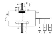
- FIG. 3 shows a schematic configuration of an example of a DC magnetron sputtering apparatus used for laminating the AlNO buffer layer 2 on the surface of the substrate 1.
- the DC magnetron sputtering apparatus includes a chamber 21, a heater 23 installed below the inside of the chamber 21, a cathode 28 installed so as to face the heater 23, and a gas inside the chamber 21. And an exhaust port 25 for discharging to the outside.
- the heater 23 is supported by a heater support 24. Further, the cathode 28 has an Al target 26 made of aluminum and a magnet 27 supported by a magnet support material 29.
- the chamber 21 is supplied with a mass flow controller 30 for supplying argon gas into the chamber 21, a mass flow controller 31 for supplying nitrogen gas into the chamber 21, and oxygen gas is supplied into the chamber 21. And a mass flow controller 32 for connection.
- the substrate 1 In laminating the AlNO buffer layer 2 on the surface of the substrate 1, first, the substrate 1 is placed on the heater 23 in the DC magnetron sputtering apparatus having the above configuration. The substrate 1 is disposed with a predetermined distance d so that the growth surface of the substrate 1 (surface on which the AlNO buffer layer 2 is grown) faces the surface of the Al target 26.
- the distance d means the shortest distance between the center of the surface of the Al target 26 and the growth surface of the substrate 1, and the distance d is preferably 100 mm or more and 250 mm or less, and 120 mm or more. More preferably, it is 210 mm or less, and further preferably 150 mm or more and 180 mm or less. This is because high energy reactive species are supplied to the substrate 1 when the AlNO buffer layer 2 is deposited by DC magnetron sputtering, but when the distance d is 100 mm or more, the reactive species are Damage to the growth surface of the substrate 1 can be reduced. When the distance d is 250 mm or less, plasma discharge is likely to occur and the formation rate of the AlNO buffer layer 2 is increased.
- the AlNO buffer layer 2 having good crystallinity composed of an aggregate of columnar crystals with aligned crystal grains extending in the normal direction (vertical direction) of the growth surface can be laminated. Therefore, by growing a nitride semiconductor layer on the surface of such a good crystalline AlNO buffer layer 2, a nitride semiconductor layer having a low dislocation density and excellent crystallinity (in this embodiment, a nitride semiconductor layer).
- the underlayer 3) can be obtained with good reproducibility, and thus a nitride semiconductor device having good characteristics can be produced with good reproducibility.
- the AlNO buffer layer 2 having good crystallinity can be stacked.
- a nitride semiconductor layer having a low dislocation density and excellent crystallinity can be grown with good reproducibility.
- a nitride semiconductor device having good characteristics can be produced with good reproducibility. growing.
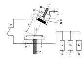
- FIG. 4 shows a schematic configuration of another example of a DC magnetron sputtering apparatus used for laminating the AlNO buffer layer 2 on the surface of the substrate 1.
- the DC magnetron sputtering apparatus having the configuration shown in FIG. 4 is characterized in that the Al target 26 is inclined with respect to the growth surface of the substrate 1 with a space between the substrate 1 and the Al target 26.
- the Al target 26 is disposed so as to be inclined by an angle ⁇ with respect to the normal direction of the growth surface of the substrate 1.
- the angle ⁇ is preferably 10 ° to 45 °, and more preferably 20 ° to 45 °.
- the DC-continuous is placed between the substrate 1 and the Al target 26.
- the AlNO buffer layer 2 is stacked by DC magnetron sputtering with a voltage applied according to the method, damage to the growth surface of the substrate 1 due to high energy reactive species supplied to the substrate 1 when the AlNO buffer layer 2 is stacked. Therefore, the AlNO buffer layer 2 having excellent crystallinity tends to be stacked. Furthermore, the crystallinity and layer thickness of the AlNO buffer layer 2 tend to be uniform in the plane of the substrate 1.
- the shortest distance d between the center of the surface of the Al target 26 and the growth surface of the substrate 1 is preferably 100 mm or more and 250 mm or less, and 120 mm or more and 210 mm. More preferably, it is more preferably 150 mm or more and 180 mm or less. Also in the DC magnetron sputtering apparatus having the configuration shown in FIG. 4, by setting the shortest distance d as described above, the AlNO buffer layer 2 excellent in crystallinity tends to be laminated for the reasons described above. is there.
- the DC-continuous method is a method in which a DC voltage having a predetermined magnitude (a voltage whose direction does not change with time) is continuously applied between the substrate 1 and the Al target 26 during the sputtering of the Al target 26. is there.
- the AlNO buffer layer 2 As described above, while continuously introducing nitrogen gas and oxygen gas into the chamber 21 and continuously exhausting the gas inside the chamber 21 from the exhaust port 25 to the outside of the chamber 21,
- the AlNO buffer layer 2 is formed by reactive sputtering using an Al target 26 as a target, a dislocation capable of forming a nitride semiconductor layer having excellent crystallinity above it with good reproducibility.
- the present inventors have found that an AlNO buffer layer 2 having a low density and good crystallinity can be formed, and the present invention has been completed. This is because the atmosphere inside the chamber 21 is kept fresh by continuously introducing and exhausting oxygen gas and nitrogen gas at a flow rate into the chamber 21. It is considered that this is because the ratio of the gas generated from the inner wall of the chamber 21 in the gas is reduced.
- the AlNO buffer layer 2 is formed in an atmosphere where the ratio of the flow rate of oxygen gas to the total of the flow rate of nitrogen gas and the flow rate of oxygen gas is 0.5% or less, and is formed in an atmosphere where the flow rate is 0.25% or less. It is more preferable.
- the ratio of the flow rate of oxygen gas to the total of the flow rate of nitrogen gas and the flow rate of oxygen gas is 0.5% or less, particularly when it is 0.25% or less, a good crystalline AlNO buffer layer 2 Therefore, a nitride semiconductor layer having a low dislocation density and excellent crystallinity is likely to be grown on the surface of such an AlNO buffer layer 2 with good reproducibility, and thus good characteristics. The tendency to be able to manufacture nitride semiconductor devices having high reproducibility is increased.
- the AlNO buffer layer 2 is preferably formed in an atmosphere in which the ratio of the flow rate of oxygen gas to the total of the flow rate of nitrogen gas and the flow rate of oxygen gas is 0.05% or more, and 0.1% or more. More preferably, it is formed in an atmosphere.
- the ratio of the oxygen gas flow rate to the total of the nitrogen gas flow rate and the oxygen gas flow rate is 0.05% or more, particularly 0.1% or more, a good crystalline AlNO buffer layer 2 is obtained. Therefore, a nitride semiconductor layer having a low dislocation density and excellent crystallinity is likely to be grown on the surface of such an AlNO buffer layer 2 with good reproducibility, and thus good characteristics. The tendency to be able to manufacture nitride semiconductor devices having high reproducibility is increased.
- the present invention is not limited to this.
- at least a part of the nitrogen gas may be replaced with ammonia gas. Good.
- the AlNO buffer layer 2 is preferably formed so as to cover 90% or more of the surface of the substrate 1.
- the AlNO buffer layer 2 covers 90% or more of the surface of the substrate 1, the generation of hillocks and pits in the nitride semiconductor layer formed on the AlNO buffer layer 2 is suppressed. Tend to be able to.
- the AlNO buffer layer 2 is preferably formed so that the oxygen concentration in the AlNO buffer layer 2 is 1 atomic% or more and 10 atomic% or less, and is preferably formed so that it is 2 atomic% or more and 9 atomic% or less. Is more preferable, and it is more preferable that they are 3 atomic% or more and 7 atomic% or less.
- the oxygen concentration in the buffer layer 2 was supposed to be 1 atomic% or less, but as a result of intensive studies by the present inventors, the oxygen concentration in the AlNO buffer layer 2 was Nitride having a low dislocation density and excellent crystallinity when it is 1 atom% or more and 10 atom% or less, further 2 atom% or more and 9 atom% or less, particularly 3 atom% or more and 7 atom% or less. This is because the tendency that the semiconductor layer can be grown with high reproducibility is increased, and as a result, the tendency that nitride semiconductor elements having even better characteristics can be manufactured with high reproducibility has been found to increase.
- the AlNO buffer layer 2 is preferably formed so that the oxygen concentration in the AlNO buffer layer 2 is uniform in the AlNO buffer layer 2.
- a nitride semiconductor layer having a low dislocation density and excellent crystallinity is likely to be grown with good reproducibility.
- a nitride semiconductor device having even better characteristics can be manufactured with good reproducibility. It tends to be possible.
- the oxygen concentration in the AlNO buffer layer 2 is uniform in the AlNO buffer layer 2
- the oxygen concentration in the portion where the oxygen concentration is maximum in the AlNO buffer layer 2 and the oxygen concentration in the AlNO buffer layer 2 are used.
- the difference from the oxygen concentration in the portion where the minimum is 10 may be 10 atomic% or less.
- the refractive index of light with a wavelength of 450 nm of the AlNO buffer layer 2 is preferably 2 or more and 2.1 or less, more preferably 2.03 or more and 2.08 or less, and 2.03 or more and 2.05 or less. It is more preferable.
- the refractive index of the AlNO buffer layer 2 with respect to light having a wavelength of 450 nm is 2 or more and 2.1 or less, further 2.03 or more and 2.08 or less, particularly 2.03 or more and 2.05 or less.
- the thickness of the AlNO buffer layer 2 stacked on the growth surface of the substrate 1 is preferably 5 nm or more and 100 nm or less.
- the thickness of the AlNO buffer layer 2 is less than 5 nm, the AlNO buffer layer 2 may not sufficiently function as a buffer layer.
- the thickness of the AlNO buffer layer 2 exceeds 100 nm, the function as the buffer layer is not improved, and only the formation time of the AlNO buffer layer 2 may be increased.
- the thickness of the AlNO buffer layer 2 is more preferably 10 nm or more and 50 nm or less.
- the temperature of the substrate 1 when the AlNO buffer layer 2 is laminated is preferably 300 ° C. or higher and 1000 ° C. or lower.
- the temperature of the substrate 1 when the AlNO buffer layer 2 is stacked is less than 300 ° C., the AlNO buffer layer 2 cannot sufficiently cover the growth surface of the substrate 1, and the growth surface of the substrate 1 is the AlNO buffer layer. 2 is likely to be exposed.
- the temperature of the substrate 1 when the AlNO buffer layer 2 is stacked exceeds 1000 ° C., the migration of the raw material on the growth surface of the substrate 1 becomes too active, rather than a columnar crystal aggregate.
- the AlNO buffer layer 2 close to a crystal film is formed, and the function of the AlNO buffer layer 2 as a buffer layer may be reduced.
- the pressure inside the chamber 21 immediately before sputtering is 1 ⁇ . It is preferably 10 ⁇ 4 Pa or less. That is, it is preferable that the pressure of the atmosphere immediately before the formation of the AlNO buffer layer is 1 ⁇ 10 ⁇ 4 Pa or less.
- ⁇ Dummy discharge> In order to further improve the ultimate vacuum of the chamber 21, it is preferable to perform a dummy discharge in the chamber 21 before the formation of the AlNO buffer layer 2. By performing such a dummy discharge, it is possible to previously remove impurities knocked out of the chamber 21.
- a dummy discharge method for example, a method of performing a discharge program similar to the process at the time of forming the AlNO buffer layer 2 without introducing the substrate 1 can be used.
- Such a dummy discharge can be performed under conditions similar to the conditions for forming the AlNO buffer layer 2 as well as under conditions where impurities can be easily ejected.
- Examples of such conditions include a condition for setting the set temperature for heating the substrate high, and a condition for setting the power for generating plasma high.
- Dummy discharge that repeats alternately the process of supplying only argon gas and the process of supplying gas at the time of forming the AlNO buffer layer 2 while plasma is continuously generated in the chamber 21 is also effective in improving the ultimate vacuum. It is.
- this dummy discharge it is important to thinly coat the inner wall of the chamber 21 with an aluminum-rich metal film in the process of supplying only argon gas. This is because an aluminum-rich metal film easily adsorbs impurities.
- the last step of the dummy discharge ends with a step of supplying a gas having a condition for forming the AlNO buffer layer 2.
- the ultimate vacuum in the chamber 21 before the film formation of the AlNO buffer layer 2 is further increased, so that the oxygen-containing substances existing in the inner wall and space of the chamber 21 can be more reliably obtained. It can be removed and reduced.
- the pressure inside the chamber 21 when the AlNO buffer layer 2 is stacked is preferably 0.2 Pa or more.
- the pressure inside the chamber 21 when the AlNO buffer layer 2 is stacked is less than 0.2 Pa, the amount of nitrogen inside the chamber 21 decreases, and the aluminum sputtered from the Al target 26 does not become nitride. There is a risk of adhering to the growth surface of the substrate 1 in a state.
- the upper limit of the pressure inside the chamber 21 when the AlNO buffer layer 2 is stacked is not particularly limited, and may be a pressure that can generate plasma inside the chamber 21.
- the formation rate of the AlNO buffer layer 2 is preferably 0.01 nm / second or more and 1 nm / second or less.
- the formation rate of the AlNO buffer layer 2 is less than 0.01 nm / second, the AlNO buffer layer 2 spreads uniformly on the growth surface of the substrate 1 and grows in an island shape without growing, and the growth surface of the substrate 1 Cannot be uniformly covered by the AlNO buffer layer 2, and the growth surface of the substrate 1 may be exposed from the AlNO buffer layer 2.
- the formation rate of the AlNO buffer layer 2 exceeds 1 nm / second, the AlNO buffer layer 2 becomes amorphous, and a dislocation density is small on the AlNO buffer layer 2 and has excellent crystallinity. There is a possibility that the layer cannot be grown.
- the nitride semiconductor base layer 3 is laminated on the surface of the AlNO buffer layer 2 by MOCVD (Metal Organic Chemical Vapor Deposition) method.
- MOCVD Metal Organic Chemical Vapor Deposition
- nitride semiconductor underlayer 3 for example, a nitride semiconductor layer made of a group III nitride semiconductor represented by the formula Al x1 Ga y1 In z1 N (0 ⁇ x1 ⁇ 1, 0 ⁇ y1 ⁇ 1, 0 ⁇ z1 ⁇ ). 1, x1 + y1 + z1 ⁇ 0), but in order not to inherit crystal defects such as dislocations in the AlNO buffer layer 2 made up of columnar crystals, Ga or In is included as a group III element. It is preferable.
- the nitride semiconductor underlayer 3 is a group III nitride containing Ga or In.
- a dislocation loop tends to occur. Therefore, by using the nitride semiconductor underlayer 3 made of a group III nitride semiconductor containing Ga or In, dislocations are looped and confined in the vicinity of the interface with the AlNO buffer layer 2, and the nitride semiconductor from the AlNO buffer layer 2 is confined. It is possible to suppress dislocations from being taken over by the underlayer 3.
- the nitride semiconductor underlayer 3 is made of a group III nitride semiconductor represented by the formula of Al x1 Ga y1 N (0 ⁇ x1 ⁇ 1, 0 ⁇ y1 ⁇ 1), particularly when made of GaN, AlNO Since dislocations can be looped and confined in the vicinity of the interface with the buffer layer 2, the nitride semiconductor underlayer 3 having a low dislocation density and good crystallinity tends to be obtained.
- the surface of the AlNO buffer layer 2 immediately before the nitride semiconductor underlayer 3 is laminated may be heat-treated.
- This heat treatment can be performed in an MOCVD apparatus using, for example, the MOCVD method, and for example, hydrogen gas or nitrogen gas can be used as the atmospheric gas during the heat treatment.
- hydrogen gas or nitrogen gas can be used as the atmospheric gas during the heat treatment.
- ammonia gas may be mixed with the atmospheric gas during the heat treatment.
- the above heat treatment can be performed, for example, at a temperature of 900 ° C. or higher and 1250 ° C. or lower for a time period of 1 minute to 60 minutes, for example.
- the nitride semiconductor underlayer 3 may be doped with an n-type dopant in the range of 1 ⁇ 10 17 cm ⁇ 3 to 1 ⁇ 10 19 cm ⁇ 3, but from the viewpoint of maintaining good crystallinity.
- the nitride semiconductor underlayer 3 is preferably undoped.
- the n-type dopant for example, silicon, germanium, tin, and the like can be used, and it is preferable to use silicon and / or germanium.
- the temperature of the substrate 1 when the nitride semiconductor underlayer 3 is stacked is preferably 800 ° C. or higher and 1250 ° C. or lower, and more preferably 1000 ° C. or higher and 1250 ° C. or lower.
- the temperature of the substrate 1 when the nitride semiconductor underlayer 3 is stacked is 800 ° C. or higher and 1250 ° C. or lower, particularly when the temperature is 1000 ° C. or higher and 1250 ° C. or lower, the nitride semiconductor underlayer 3 having excellent crystallinity is formed. It tends to be able to grow.
- an n-type nitride semiconductor contact layer 4 an n-type nitride semiconductor clad layer 5
- a nitride is formed on the surface of the nitride semiconductor underlayer 3 by MOCVD.
- the semiconductor active layer 6, the p-type nitride semiconductor clad layer 7, and the p-type nitride semiconductor contact layer 8 are stacked in this order to form a stacked body.
- n-type nitride semiconductor contact layer for example, a nitride semiconductor layer made of a group III nitride semiconductor represented by the formula of Al x2 Ga y2 In z2 N (0 ⁇ x2 ⁇ 1, 0 ⁇ y2 ⁇ 1, 0 ⁇ z2 ⁇ 1, x2 + y2 + z2 ⁇ 0), and a layer doped with an n-type dopant can be stacked.
- the n-type nitride semiconductor contact layer 4 has an Al x2 Ga 1-x2 N (0 ⁇ x2 ⁇ 1, preferably 0 ⁇ x2 ⁇ 0.5, more preferably 0 ⁇ x2 ⁇ 0.1) formula.
- the doping concentration of the n-type dopant to the n-type nitride semiconductor contact layer 4 is such that good ohmic contact with the n-side electrode 11 is maintained, cracking is suppressed in the n-type nitride semiconductor contact layer 4 and good crystallinity is achieved. From the viewpoint of maintaining the above, it is preferably within the range of 5 ⁇ 10 17 cm ⁇ 3 or more and 5 ⁇ 10 19 cm ⁇ 3 or less.
- the total thickness of the nitride semiconductor underlayer 3 and the n-type nitride semiconductor contact layer 4 is preferably 4 ⁇ m or more and 20 ⁇ m or less from the viewpoint of maintaining good crystallinity of these layers. Or less, more preferably 6 ⁇ m or more and 15 ⁇ m or less.
- the crystallinity of these layers deteriorates or pits are formed on the surfaces of these layers. May occur.
- the warpage of the substrate 1 becomes large, and the yield of the device may be reduced. .
- n-type nitride semiconductor cladding layer As the n-type nitride semiconductor cladding layer 5, for example, a nitride semiconductor layer made of a group III nitride semiconductor represented by the formula of Al x3 Ga y3 In z3 N (0 ⁇ x3 ⁇ 1, 0 ⁇ y3 ⁇ 1, 0 ⁇ z3 ⁇ 1, x3 + y3 + z3 ⁇ 0) and a layer doped with an n-type dopant can be stacked.
- a nitride semiconductor layer made of a group III nitride semiconductor represented by the formula of Al x3 Ga y3 In z3 N (0 ⁇ x3 ⁇ 1, 0 ⁇ y3 ⁇ 1, 0 ⁇ z3 ⁇ 1, x3 + y3 + z3 ⁇ 0) and a layer doped with an n-type dopant can be stacked.
- the n-type nitride semiconductor clad layer 5 may have a structure in which a plurality of nitride semiconductor layers made of a group III nitride semiconductor are heterojunction or a superlattice structure.
- the band gap of the n-type nitride semiconductor cladding layer 5 is preferably larger than the band gap of the nitride semiconductor active layer 6 from the viewpoint of light confinement in the nitride semiconductor active layer 6 described later.
- the thickness of n-type nitride semiconductor cladding layer 5 is not particularly limited, but is preferably 0.005 ⁇ m or more and 0.5 ⁇ m or less, more preferably 0.005 ⁇ m or more and 0.1 ⁇ m or less.
- the doping concentration of the n-type dopant into the n-type nitride semiconductor cladding layer 5 is 1 ⁇ 10 17 cm ⁇ 3 or more and 1 ⁇ 10 20 cm ⁇ 3 or less from the viewpoint of maintaining good crystallinity and reducing the operating voltage of the device. Preferably, it is 1 ⁇ 10 18 cm ⁇ 3 or more and 1 ⁇ 10 19 cm ⁇ 3 or less.
- the nitride semiconductor active layer 6 has a single quantum well (SQW) structure
- the nitride semiconductor active layer 6 is, for example, a group III nitride represented by the formula Ga 1 -z 4 In z 4 N
- a nitride semiconductor layer (0 ⁇ z4 ⁇ 0.4) made of a physical semiconductor can be used as a quantum well layer, and the In composition and thickness are controlled so as to obtain a desired emission wavelength.
- the thickness of the nitride semiconductor active layer 6 is not particularly limited, but is preferably 1 nm or more and 10 nm or less, and more preferably 1 nm or more and 6 nm or less from the viewpoint of improving the light emission output.
- the temperature of the substrate 1 when forming the nitride semiconductor active layer 6 is preferably 700 ° C. or higher and 900 ° C. or lower, and more preferably 750 ° C. or higher and 850 ° C. or lower.
- the temperature of the substrate 1 when forming the nitride semiconductor active layer 6 is less than 700 ° C., the crystallinity of the nitride semiconductor active layer 6 may be deteriorated. Sublimation becomes prominent, and the incorporation efficiency of In into the solid phase may be reduced, leading to fluctuations in the In composition.
- nitride semiconductor active layer 6 for example, a nitride semiconductor layer (0 ⁇ z4 ⁇ 0.4) made of a group III nitride semiconductor represented by the formula Ga 1 -z4 In z4 N is used as a quantum well layer.
- Nitride semiconductor layers (0 ⁇ x5 ⁇ 1, 0 ⁇ y5 ⁇ 1, 0 ⁇ z5 ⁇ 1, nitride semiconductor layers represented by the formula Al x5 Ga y5 In z5 N having a larger band gap than this well layer x5 + y5 + z5 ⁇ 0) may be used as a quantum barrier layer, and a layer having a multiple quantum well (MQW) structure in which these layers are alternately stacked one by one may be used.
- the above quantum well layer and / or quantum barrier layer may be doped with an n-type or p-type dopant.
- a layer doped with a p-type dopant in z6 ⁇ 1, x6 + y6 + z6 ⁇ 0, and the like can be stacked, and in particular, a nitride semiconductor layer made of a group III nitride semiconductor represented by the formula of Al x6 Ga 1-x6 N ( It is preferable to stack a layer doped with a p-type dopant at 0 ⁇ x6 ⁇ 0.4, preferably 0.1 ⁇ x6 ⁇ 0.3.
- magnesium etc. can be used, for example.
- the band gap of the p-type nitride semiconductor cladding layer 7 is preferably larger than the band gap of the nitride semiconductor active layer 6 from the viewpoint of optical confinement in the nitride semiconductor active layer 6.
- the thickness of the p-type nitride semiconductor clad layer 7 is not particularly limited, but is preferably 0.01 ⁇ m or more and 0.4 ⁇ m or less, more preferably 0.02 ⁇ m or more and 0.1 ⁇ m or less.
- the doping concentration of the p-type dopant in the p-type nitride semiconductor cladding layer 7 is 1 ⁇ 10 18 cm ⁇ 3 or more and 1 ⁇ 10 21 cm. ⁇ 3 or less, preferably 1 ⁇ 10 19 cm ⁇ 3 or more and 1 ⁇ 10 20 cm ⁇ 3 or less.
- ⁇ P-type nitride semiconductor contact layer As the p-type nitride semiconductor contact layer 8, for example, a nitride semiconductor layer made of a group III nitride semiconductor represented by the formula of Al x7 Ga y7 In z7 N (0 ⁇ x7 ⁇ 1, 0 ⁇ y7 ⁇ 1, 0 ⁇ z7 ⁇ 1, x7 + y7 + z7 ⁇ 0), a layer doped with a p-type dopant can be stacked, and in particular, using a layer doped with a p-type dopant in a GaN layer can maintain good crystallinity and have good ohmic resistance. It is preferable from the viewpoint of obtaining contact.
- the doping concentration of the p-type dopant to the p-type nitride semiconductor contact layer 8 is determined from the viewpoint of maintaining good ohmic contact, suppressing the occurrence of cracks in the p-type nitride semiconductor contact layer 8, and maintaining good crystallinity. It is preferably in the range of 1 ⁇ 10 18 cm ⁇ 3 to 1 ⁇ 10 21 cm ⁇ 3 and more preferably in the range of 5 ⁇ 10 19 cm ⁇ 3 to 5 ⁇ 10 20 cm ⁇ 3. .
- the thickness of the p-type nitride semiconductor contact layer 8 is not particularly limited, but is 0.01 ⁇ m or more and 0.5 ⁇ m or less from the viewpoint of improving the light emission output of the nitride semiconductor light emitting diode element 100. It is preferably 0.05 ⁇ m or more and 0.2 ⁇ m or less.
- n-type nitride semiconductor contact layer 4 The n-type nitride semiconductor contact layer 4, the n-type nitride semiconductor clad layer 5, the nitride semiconductor active layer 6, the p-type nitride semiconductor clad layer 7 and the p-type nitride semiconductor contact layer 8 are each a group III nitride. When composed of a semiconductor, these layers are laminated by, for example, the MOCVD method as follows.
- TMG trimethylgallium
- TMA trimethylaluminum
- TMI trimethylindium
- doping silicon which is an n-type dopant, for example, silane (SiH 4 ) or disilane (Si 2 H 4 ) is added as a doping gas to the inside of the reactor of the MOCVD apparatus and supplied. By doing so, it is possible to dope silicon.
- CP 2 Mg biscyclopentadienyl magnesium
- a translucent electrode layer made of, for example, ITO (Indium Tin Oxide), ZnO, or IZO (Indium Zinc Oxide) is formed on the surface of the p-type nitride semiconductor contact layer 8.
- the p-side electrode 10 is formed on the surface of the translucent electrode layer 9.
- a part of the stacked body after the formation of the p-side electrode 10 is removed by etching, so that a part of the surface of the n-type nitride semiconductor contact layer 4 is exposed.
- the n-side electrode 11 is formed on the exposed surface of the n-type nitride semiconductor contact layer 4, whereby the nitride semiconductor light-emitting diode device 100 of the embodiment can be manufactured. .
- the columnar crystal with aligned crystal grains extending in the normal direction (vertical direction) of the growth surface of the substrate 1 is used.
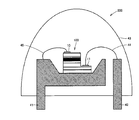
- FIG. 8 is a schematic cross-sectional view of an example of a light emitting device using the nitride semiconductor light emitting diode element 100 of the embodiment.
- the light emitting device 200 having the configuration shown in FIG. 8 has a configuration in which the nitride semiconductor light emitting diode element 100 of the embodiment is installed on the first lead frame 41.
- the p-side electrode 10 of the nitride semiconductor light-emitting diode element 100 and the first lead frame 41 are electrically connected by the first wire 45 and the n-side electrode 11 of the nitride semiconductor light-emitting diode element 100.
- the second lead frame 42 are electrically connected by a second wire 44.
- the nitride semiconductor light-emitting diode element 100 is molded with a transparent mold resin 43, so that the light-emitting device 200 has a shell shape.
- the light emitting device having the configuration shown in FIG. 8 uses the nitride semiconductor light emitting diode element 100 according to the embodiment, the light emitting device can have a low operating voltage and a high light emission output.
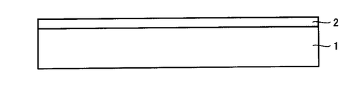
- Example 1 As shown in FIG. 2, an AlNO buffer layer 2 is laminated on a substrate 1 made of a sapphire substrate having a flat surface by a reactive sputtering method using the sputtering apparatus shown in FIG. 3 under various conditions. The characteristics of each AlNO buffer layer 2 were investigated. Further, a nitride semiconductor underlayer 3 made of undoped GaN was stacked on each AlNO buffer layer 2 by MOCVD, and the characteristics of each nitride semiconductor underlayer 3 were investigated.
- argon gas whose flow rate is controlled by the mass flow controller 30 is supplied into the chamber 21 without the substrate 1 made of a sapphire substrate being installed on the heater 23 of the sputtering apparatus shown in FIG.
- the inside of the chamber 21 was kept at a constant pressure by exhausting the same amount of gas as the supplied argon gas from the exhaust port 25 using a vacuum pump.
- plasma of argon gas was generated between the heater 23 and the Al target 26 by applying a voltage between the heater 23 and the Al target 26.
- An argon gas plasma was generated for several minutes, and the inner wall of the chamber 21 was thinly coated with an aluminum-rich metal film. Furthermore, the argon gas plasma was maintained, and the argon gas was switched to the nitrogen gas. At this time, it is preferable that the fluctuation of the pressure inside the chamber 21 is small. Subsequently, the plasma was held for several minutes while nitrogen plasma was generated, and the inner wall of the chamber 21 was coated with an AlN film.
- plasma of nitrogen gas and oxygen gas was generated between the substrate 1 and the Al target 26 by applying a voltage between the substrate 1 and the Al target 26.
- aluminum of the Al target 26 is sputtered, and reactive sputtering in which aluminum reacts with oxygen and nitrogen in the plasma is performed.
- a compound of aluminum, nitrogen and oxygen is formed on the entire surface of the substrate 1.
- An AlNO buffer layer 2 having a thickness of 25 nm was formed. At this time, the formation rate of the AlNO buffer layer 2 was 0.04 nm / second.
- the pressure inside the chamber 21 immediately before sputtering was 1 ⁇ 10 ⁇ 4 Pa or less. Further, the pressure inside the chamber 21 when the AlNO buffer layer 2 was laminated was set to an atmospheric pressure of 0.2 Pa or more.
- the AlNO buffer layer 2 of the samples 1 to 6 is formed under various conditions shown in the column of the film forming condition of the AlNO buffer layer in Table 1, and the X of the AlNO buffer layer 2 of the samples 1 to 6 is formed.
- the line half width [arcsec], oxygen concentration [atomic%] and refractive index were measured. The results are shown in Table 1.
- the X-ray half width [arcsec] in Table 1 indicates the rocking curve detected by X-ray diffraction measurement for the (002) plane of the AlN crystal, the (004) plane of the GaN crystal, and the (102) plane of the GaN crystal, respectively. Calculation was made by measuring the half-value width of the corresponding peak when the reflecting surface was used. As the X-ray half width is smaller, the crystal is considered to be a good crystal with fewer dislocations. Therefore, this value is used as a scale for evaluating crystallinity.
- the oxygen concentration [atomic%] in Table 1 was measured by XPS (X-ray photoelectron spectroscopy).
- the refractive index in Table 1 indicates the refractive index with respect to light having a wavelength of 450 nm, and was measured with a spectroscopic ellipsometer.
- the substrate 1 after the lamination of the AlNO buffer layer 2 was taken out from the chamber 21 of the sputtering apparatus shown in FIG. 3 and installed in the reactor of the MOCVD apparatus.
- the temperature of the substrate 1 was raised to 1125 ° C. over about 15 minutes while supplying nitrogen gas and hydrogen gas as carrier gases.
- the internal pressure of the reaction furnace was normal pressure, and the flow rate ratio of hydrogen gas and nitrogen gas (carrier gas flow rate / nitrogen gas flow rate) as carrier gas was 50/50.
- the supply of TMG (trimethylgallium) gas into the reactor was started, and the surface of the AlNO buffer layer 2 as shown in FIG.
- a nitride semiconductor underlayer (GaN layer) 3 made of undoped GaN having a thickness of 5 ⁇ m was stacked thereon by MOCVD.
- the GaN layers 3 of the samples 1 to 6 are formed on the respective surfaces of the AlNO buffer layers 2 of the samples 1 to 6, and the (004) plane of the GaN crystal of the GaN layers 3 of the samples 1 to 6 and The X-ray half width [arcsec] with the (102) plane of the GaN crystal as the reflecting surface was measured. The results are shown in Table 1.
- the X-ray half width of the AlN (002) plane is 300 [arcsec] or less and the refractive index is 2.08 or less. Met. From the above, it was confirmed that in the formation of the AlNO buffer layer by reactive sputtering, the oxygen gas flow rate ratio (oxygen gas flow rate ⁇ 100 / total flow rate of all gases) is preferably 0.5% or less.
- Patent Document 6 the amount of oxygen inevitably present in the AlN buffer layer is reduced as much as possible to obtain a high-quality nitride semiconductor device, but the present inventors conversely actively Oxygen is introduced to form the AlNO buffer layer 2 and a nitride semiconductor layer is directly formed on the surface to obtain a high-quality nitride semiconductor device.
- the reason why good results were obtained by such a method is as follows, although there is no confirmation.
- oxygen high-purity oxygen
- residual oxygen oxygen in which the remaining oxygen-containing material such as the inner wall of the chamber 21 was originally sputtered during sputtering.
- Residual oxygen is generally considered to be generated by the decomposition of moisture adsorbed on the inner wall of the chamber, and the forms thereof are H 2 O itself, OH (neutral or ion), and O (neutral or ion). Conceivable.
- high-purity oxygen is considered to be O 2 itself, O 2 ion, or O (neutral or ion).
- high-purity oxygen is included in the AlNO buffer layer 2 in the form of O 2 , or is included in the AlNO buffer layer 2 in a state that does not contain hydrogen, and thus is estimated to have different properties from the AlN film mixed with residual oxygen. Is done.
- the nitridation is formed directly on the oxygen-filled gap (crystal grain boundary) of the columnar AlN crystals forming the AlNO buffer layer 2. It is considered that the dislocation density of the physical semiconductor layer is reduced. And, it is considered that high purity oxygen works well to fill the crystal grain boundaries.
- the present invention is not limited to this.
- at least part of the nitrogen gas may be replaced with argon gas.
- FIG. 9 shows a schematic cross-sectional view of the nitride semiconductor light-emitting diode element of Example 2.
- the nitride semiconductor light-emitting diode element 300 of Example 2 includes a sapphire substrate 1 whose surface is processed to be uneven, an AlNO buffer layer 2 disposed in contact with the surface of the sapphire substrate 1, and an AlNO buffer layer 2 Nitride semiconductor underlayer 3 placed in contact with the surface of the semiconductor, n-type nitride semiconductor contact layer 4 placed in contact with the surface of the nitride semiconductor underlayer 3, and the surface of n-type nitride semiconductor contact layer 4 N-type nitride semiconductor cladding layer 5 placed in contact with the surface, nitride semiconductor active layer 6 placed in contact with the surface of n-type nitride semiconductor cladding layer 5, and the surface of nitride semiconductor active layer 6
- the p-type nitride semiconductor clad layer 7 installed in this manner, the p-
- the sapphire substrate 1 has an uneven shape for the purpose of improving the crystal quality of the nitride semiconductor underlayer 3 and light scattering at the interface.
- the depth of the uneven shape is preferably sufficiently deeper than the thickness of the AlNO buffer layer 2.
- the nitride semiconductor underlayer 3 is also preferably formed along an uneven shape, the depth of the unevenness is preferably 0.3 ⁇ m or more and 3 ⁇ m or less.
- interval of a convex part is 2 micrometers or more and 5 micrometers or less.
- the cross-sectional shape of the convex portion may be trapezoidal, but the upper portion of the convex portion may be rounded.
- the sapphire substrate 1 shown in FIG. 9 was placed on a heater 23 provided in the chamber 21 of a DC magnetron sputtering apparatus that is performed by applying a voltage by the DC-continuous method shown in FIG.
- the substrate 1 was installed so that the c-plane of the sapphire substrate 1 faces the surface of the Al target 26 and the shortest distance d between the center of the surface of the Al target 26 and the c-plane of the sapphire substrate 1 is 180 mm. . Thereafter, the sapphire substrate 1 was heated to a temperature of 550 ° C. by the heater 23. The pressure inside the chamber 21 immediately before sputtering was 3 ⁇ 10 ⁇ 5 Pa or less.
- nitrogen gas is supplied into the chamber 21 of the DC magnetron sputtering apparatus at a flow rate of 40 sccm and oxygen gas is supplied at a flow rate of 0.02 sccm, and the pressure is maintained at 0.4 Pa. Thereafter, the temperature of the sapphire substrate 1 is maintained at 550 ° C. did.
- AlNO buffer layer 2 having a thickness of 30 nm made of an aggregate of columnar crystals of aluminum oxynitride (AlON) was laminated on the c-plane of the sapphire substrate 1. At this time, the formation rate of the AlNO buffer layer 2 was 0.04 nm / second.
- the magnet 27 in the cathode 28 of the DC magnetron sputtering apparatus shown in FIG. 4 was swung both in the nitriding of the c-plane of the sapphire substrate 1 and in the lamination of the AlNO buffer layer 2.
- the AlNO buffer layer 2 is stacked for a predetermined time in accordance with the AlNO buffer layer 2 deposition rate measured in advance, and the nitrogen plasma is stopped when the thickness of the AlNO buffer layer 2 reaches 30 nm. did.
- the sapphire substrate 1 after the lamination of the AlNO buffer layer 2 was taken out from the chamber 21 of the DC magnetron sputtering apparatus and installed in the reactor of the MOCVD apparatus.
- the sapphire substrate 1 after the lamination of the AlNO buffer layer 2 was placed on a graphite susceptor in order to be heated by a high-frequency induction heating heater.
- the sapphire substrate 1 after the AlNO buffer layer 2 is stacked is heated by a resistance heater
- the sapphire substrate 1 after the AlNO buffer layer 2 is stacked is made of quartz placed on a susceptor made of graphite. Installed on the tray.
- the temperature of the sapphire substrate 101 was raised to 1125 ° C. over about 15 minutes while supplying nitrogen gas and hydrogen gas as carrier gases while supplying ammonia gas into the reactor.
- the internal pressure of the reaction furnace was normal pressure, and the flow rate ratio of hydrogen gas and nitrogen gas (carrier gas flow rate / nitrogen gas flow rate) as carrier gas was 50/50.
- the supply of TMG gas into the reactor was started, and as shown in FIG. 9, the thickness of the sapphire substrate 101 was increased on the surface of the AlNO buffer layer 2.
- a GaN foundation layer 3 made of undoped GaN having a thickness of 4 ⁇ m was laminated by the MOVPE method.
- the ammonia gas was supplied into the reactor so that the molar ratio of the group V element to the group III element (number of moles of group V element / number of moles of group III element) was 1500.
- the temperature of the sapphire substrate 1 is set to 1125 ° C., and silane gas is supplied into the reactor so that the Si doping concentration is 1 ⁇ 10 19 / cm 3 .
- a Si-doped n-type GaN contact layer 4 having a thickness of 3 ⁇ m was laminated on the surface of the base layer 3 by the MOVPE method.
- the temperature of the sapphire substrate 1 was lowered to 800 ° C., and the carrier gas was changed from hydrogen gas to nitrogen gas.
- TMG gas, TMI gas and ammonia gas as raw material gases are supplied into the reaction furnace, and the Si doping concentration is 1 ⁇ 10 18 /
- silane gas supplied to the inside of the reactor so as to be cm 3 , an Si-doped n-type In 0.01 Ga 0.99 N cladding layer having a thickness of 8 nm is formed on the surface of the n-type GaN contact layer 4 as shown in FIG. 5 was laminated.
- a quantum well layer made of undoped In 0.15 Ga 0.85 N having a thickness of 3.5 nm is formed into a Si-doped n-type In 0.01 Ga 0.99 N cladding layer. 5 was laminated on the surface. Subsequently, the supply of silane gas was started, the supply of TMI gas was stopped, and a quantum barrier layer made of Si-doped n-type GaN having a thickness of 6 nm was stacked.
- the temperature of the sapphire substrate 1 was raised to 1100 ° C., and the carrier gas was changed from nitrogen gas to hydrogen gas. Then, the supply of TMG gas, TMA gas, and CP 2 Mg gas was started inside the reaction furnace, and then was supplied for 2 minutes, and then the supply of TMG gas and TMA gas was stopped. Thereby, a p-type Al 0.2 Ga 0.8 N clad layer 7 having a thickness of 20 nm was laminated on the surface of the MQW active layer 6.
- the supply of TMA gas was stopped while supplying ammonia gas into the reaction furnace. Thereafter, by changing the supply amounts of TMG gas and CP 2 Mg gas into the reactor, as shown in FIG. 9, the Mg-doped p-type GaN contact layer 108 having a thickness of 0.2 ⁇ m is made p-type Al 0.2. Laminated on the surface of the Ga 0.8 N cladding layer 7.
- the carrier gas supplied into the reactor was changed from hydrogen gas to nitrogen gas. Then, after confirming that the temperature of the sapphire substrate 1 became 300 ° C. or less, the sapphire substrate 1 after the lamination of the above layers was taken out from the reactor.
- the p-side bonding pad electrode 10 was formed.
- a part of the surface of the n-type GaN contact layer 4 was exposed by removing a part of the stacked body after the formation of the p-side bonding pad electrode 10 by dry etching.
- an n-side bonding pad electrode 11 was formed by laminating a nickel layer, an aluminum layer, a titanium layer, and a gold layer in this order on the exposed surface of the n-type GaN contact layer 4. .
- the sapphire substrate 1 is divided into 350 ⁇ m square chips, thereby producing the nitride semiconductor light-emitting diode device of Example 2. did.
- the forward current at 20 mA was The forward voltage was 3.0V. This forward voltage corresponds to the operating voltage of the nitride semiconductor light emitting diode element. Further, when the light emission of the nitride semiconductor light-emitting diode element of Example 2 was observed through the ITO layer 9, the light emission wavelength was 450 nm and the light emission output was 23.4 mW.
- the present invention may be suitably used for the manufacture of nitride semiconductor devices such as nitride semiconductor light emitting diode devices, nitride semiconductor laser devices, and nitride semiconductor transistor devices using group III nitride semiconductors. .
Landscapes
- Led Devices (AREA)
- Physical Vapour Deposition (AREA)
- Led Device Packages (AREA)
- Physical Deposition Of Substances That Are Components Of Semiconductor Devices (AREA)
Abstract
Priority Applications (4)
| Application Number | Priority Date | Filing Date | Title |
|---|---|---|---|
| EP11750532.1A EP2544250B1 (fr) | 2010-03-01 | 2011-02-23 | Procédé de fabrication d'élément semi-conducteur au nitrure, élément luminescent semi-conducteur au nitrure, et dispositif luminescent |
| US13/580,330 US8647904B2 (en) | 2010-03-01 | 2011-02-23 | Method for manufacturing nitride semiconductor device, nitride semiconductor light-emitting device, and light-emitting apparatus |
| CN201180022108.5A CN102884644B (zh) | 2010-03-01 | 2011-02-23 | 氮化物半导体元件的制造方法、氮化物半导体发光元件及发光装置 |
| JP2012503085A JP5399552B2 (ja) | 2010-03-01 | 2011-02-23 | 窒化物半導体素子の製造方法、窒化物半導体発光素子および発光装置 |
Applications Claiming Priority (2)
| Application Number | Priority Date | Filing Date | Title |
|---|---|---|---|
| JP2010044343 | 2010-03-01 | ||
| JP2010-044343 | 2010-03-01 |
Publications (1)
| Publication Number | Publication Date |
|---|---|
| WO2011108422A1 true WO2011108422A1 (fr) | 2011-09-09 |
Family
ID=44542076
Family Applications (1)
| Application Number | Title | Priority Date | Filing Date |
|---|---|---|---|
| PCT/JP2011/054008 Ceased WO2011108422A1 (fr) | 2010-03-01 | 2011-02-23 | Procédé de fabrication d'élément à semi-conducteurs au nitrure, élément luminescent à semi-conducteurs au nitrure, et dispositif luminescent |
Country Status (6)
| Country | Link |
|---|---|
| US (1) | US8647904B2 (fr) |
| EP (1) | EP2544250B1 (fr) |
| JP (1) | JP5399552B2 (fr) |
| CN (1) | CN102884644B (fr) |
| TW (2) | TWI573291B (fr) |
| WO (1) | WO2011108422A1 (fr) |
Cited By (10)
| Publication number | Priority date | Publication date | Assignee | Title |
|---|---|---|---|---|
| WO2013045190A1 (fr) * | 2011-09-30 | 2013-04-04 | Osram Opto Semiconductors Gmbh | Procédé pour produire une puce semiconductrice optoélectronique et puce semiconductrice optoélectronique correspondante |
| WO2013160343A1 (fr) * | 2012-04-26 | 2013-10-31 | Osram Opto Semiconductors Gmbh | Substrat épitaxial, procédé de fabrication d'un substrat épitaxial et puce semiconductrice opto-électronique comportant un substrat épitaxial |
| JP2015501526A (ja) * | 2011-09-30 | 2015-01-15 | オスラム オプト セミコンダクターズ ゲゼルシャフト ミット ベシュレンクテル ハフツングOsram Opto Semiconductors GmbH | オプトエレクトロニクス半導体チップの製造方法およびオプトエレクトロニクス半導体チップ |
| JP2015160995A (ja) * | 2014-02-27 | 2015-09-07 | シャープ株式会社 | AlNOバッファ層の製造方法および窒化物半導体素子の製造方法 |
| KR20150131217A (ko) * | 2013-03-14 | 2015-11-24 | 어플라이드 머티어리얼스, 인코포레이티드 | Gan-기반 광전자 및 전자 장치를 위한 산소 제어된 pvd aln 버퍼 |
| EP2672530A3 (fr) * | 2012-06-07 | 2015-12-23 | LG Innotek Co., Ltd. | Dispositif électroluminescent et emballage de dispositif électroluminescent |
| JP2016082079A (ja) * | 2014-10-17 | 2016-05-16 | 日本電信電話株式会社 | 窒化物半導体結晶成長方法 |
| JP2016219593A (ja) * | 2015-05-20 | 2016-12-22 | シャープ株式会社 | 窒化物半導体発光素子およびその製造方法 |
| US9620671B2 (en) | 2012-06-13 | 2017-04-11 | Sharp Kabushiki Kaisha | Nitride semiconductor light emitting element and method for manufacturing same |
| WO2019044173A1 (fr) * | 2017-08-31 | 2019-03-07 | 東芝マテリアル株式会社 | Élément électroluminescent à semi-conducteur et son procédé de fabrication |
Families Citing this family (21)
| Publication number | Priority date | Publication date | Assignee | Title |
|---|---|---|---|---|
| KR20140146887A (ko) * | 2013-06-18 | 2014-12-29 | 엘지이노텍 주식회사 | 발광소자 |
| CN105261681B (zh) * | 2015-09-08 | 2019-02-22 | 安徽三安光电有限公司 | 一种半导体元件及其制备方法 |
| CN105470357B (zh) * | 2015-12-31 | 2018-05-22 | 华灿光电(苏州)有限公司 | AlN模板、AlN模板的制备方法及AlN模板上的半导体器件 |
| CN105633233B (zh) * | 2015-12-31 | 2018-01-12 | 华灿光电(苏州)有限公司 | AlN模板、AlN模板的制备方法及AlN模板上的半导体器件 |
| CN105755536B (zh) * | 2016-02-06 | 2019-04-26 | 上海新傲科技股份有限公司 | 一种采用AlON缓冲层的氮化物的外延生长技术 |
| US10340416B2 (en) * | 2016-02-26 | 2019-07-02 | Riken | Crystal substrate, ultraviolet light-emitting device, and manufacturing methods therefor |
| CN105590839B (zh) * | 2016-03-22 | 2018-09-14 | 安徽三安光电有限公司 | 氮化物底层、发光二极管及底层制备方法 |
| CN106025026B (zh) * | 2016-07-15 | 2018-06-19 | 厦门乾照光电股份有限公司 | 一种用于发光二极管的AlN缓冲层及其制作方法 |
| US9824884B1 (en) * | 2016-10-06 | 2017-11-21 | Lam Research Corporation | Method for depositing metals free ald silicon nitride films using halide-based precursors |
| CN107946418B (zh) * | 2016-10-12 | 2019-12-03 | 兆远科技股份有限公司 | 一种紫外光发光二极管用衬底及其制作方法 |
| JP6648685B2 (ja) * | 2016-12-26 | 2020-02-14 | 豊田合成株式会社 | Iii族窒化物半導体発光素子の製造方法 |
| TWI626767B (zh) * | 2017-07-17 | 2018-06-11 | Crystalwise Tech Inc | Ultraviolet light-emitting diode and its substrate and the substrate thereof law |
| CN109309082A (zh) * | 2017-07-27 | 2019-02-05 | 兆远科技股份有限公司 | 紫外光发光二极管及其基板以及其基板的制造方法 |
| US10818818B2 (en) * | 2017-11-30 | 2020-10-27 | Epistar Corporation | Semiconductor device |
| CN109671819B (zh) * | 2018-11-30 | 2020-05-19 | 华灿光电(浙江)有限公司 | 一种GaN基发光二极管外延片及其制备方法 |
| WO2021090790A1 (fr) * | 2019-11-08 | 2021-05-14 | 出光興産株式会社 | Stratifié et dispositif semi-conducteur |
| US12610595B2 (en) * | 2021-07-02 | 2026-04-21 | Samsung Electronics Co., Ltd. | Integrated circuit device |
| CN115148873B (zh) * | 2022-06-30 | 2024-11-22 | 湘能华磊光电股份有限公司 | 半导体器件的制备方法 |
| CN117497661A (zh) * | 2022-07-25 | 2024-02-02 | 晶元光电股份有限公司 | 发光元件 |
| CN115763658A (zh) * | 2022-10-28 | 2023-03-07 | 聚灿光电科技(宿迁)有限公司 | 一种基于新型图形化衬底的led芯片及其制造方法 |
| CN116230822A (zh) * | 2022-12-09 | 2023-06-06 | 聚灿光电科技(宿迁)有限公司 | 一种图形化衬底、制备方法及led外延结构 |
Citations (11)
| Publication number | Priority date | Publication date | Assignee | Title |
|---|---|---|---|---|
| JPH0586646A (ja) | 1991-09-30 | 1993-04-06 | Maeda Corp | 梁を連設した鋼管柱の構築方法 |
| JP2001217503A (ja) * | 2000-02-03 | 2001-08-10 | Matsushita Electric Ind Co Ltd | GaN系半導体発光素子およびその製造方法 |
| JP2002009004A (ja) * | 1999-11-15 | 2002-01-11 | Matsushita Electric Ind Co Ltd | 窒化物半導体の製造方法、窒化物半導体素子の製造方法、窒化物半導体素子、半導体発光素子及びその製造方法 |
| JP2002334790A (ja) * | 2001-02-19 | 2002-11-22 | Semiconductor Energy Lab Co Ltd | 発光装置およびその作製方法 |
| JP3440873B2 (ja) | 1999-03-31 | 2003-08-25 | 豊田合成株式会社 | Iii族窒化物系化合物半導体素子の製造方法 |
| JP3700492B2 (ja) | 1999-09-21 | 2005-09-28 | 豊田合成株式会社 | Iii族窒化物系化合物半導体素子 |
| JP2006004970A (ja) | 2004-06-15 | 2006-01-05 | Nippon Telegr & Teleph Corp <Ntt> | 窒化物半導体薄膜の作製方法 |
| JP2007019504A (ja) * | 2002-09-30 | 2007-01-25 | Toshiba Corp | 絶縁膜及び電子素子 |
| JP2008297138A (ja) * | 2007-05-30 | 2008-12-11 | Sumitomo Metal Mining Co Ltd | Iii族窒化物系化合物半導体製造用基板とその製造方法 |
| JP2009081406A (ja) | 2007-09-27 | 2009-04-16 | Showa Denko Kk | Iii族窒化物半導体発光素子及びその製造方法、並びにランプ |
| JP2010040867A (ja) * | 2008-08-06 | 2010-02-18 | Showa Denko Kk | Iii族窒化物半導体積層構造体およびその製造方法 |
Family Cites Families (16)
| Publication number | Priority date | Publication date | Assignee | Title |
|---|---|---|---|---|
| JP3026087B2 (ja) | 1989-03-01 | 2000-03-27 | 豊田合成株式会社 | 窒化ガリウム系化合物半導体の気相成長方法 |
| JPH0326087A (ja) | 1989-06-23 | 1991-02-04 | Fuji Photo Film Co Ltd | 映像信号処理回路 |
| US5741724A (en) * | 1996-12-27 | 1998-04-21 | Motorola | Method of growing gallium nitride on a spinel substrate |
| US6713789B1 (en) | 1999-03-31 | 2004-03-30 | Toyoda Gosei Co., Ltd. | Group III nitride compound semiconductor device and method of producing the same |
| SG143945A1 (en) | 2001-02-19 | 2008-07-29 | Semiconductor Energy Lab | Light emitting device and method of manufacturing the same |
| JP3840207B2 (ja) | 2002-09-30 | 2006-11-01 | 株式会社東芝 | 絶縁膜及び電子素子 |
| SG142140A1 (en) * | 2003-06-27 | 2008-05-28 | Semiconductor Energy Lab | Display device and method of manufacturing thereof |
| WO2005015618A1 (fr) * | 2003-08-12 | 2005-02-17 | Nippon Telegraph And Telephone Corporation | Substrat de croissance de semi-conducteur a base de nitrure |
| WO2005106977A1 (fr) * | 2004-04-27 | 2005-11-10 | Matsushita Electric Industrial Co., Ltd. | Dispositif semi-conducteur en nitrure et procédé pour la fabrication de celui-ci |
| JP2006190716A (ja) * | 2004-12-28 | 2006-07-20 | Seiko Epson Corp | 強誘電体メモリ素子およびその製造方法 |
| JP2007258258A (ja) * | 2006-03-20 | 2007-10-04 | Nippon Telegr & Teleph Corp <Ntt> | 窒化物半導体素子ならびにその構造および作製方法 |
| JP4444304B2 (ja) * | 2006-04-24 | 2010-03-31 | シャープ株式会社 | 窒化物半導体発光素子および窒化物半導体発光素子の製造方法 |
| JP5205265B2 (ja) * | 2006-07-19 | 2013-06-05 | 日本碍子株式会社 | Iii族窒化物結晶の転位低減方法およびエピタキシャル成長用基板 |
| JP5311830B2 (ja) * | 2008-01-07 | 2013-10-09 | キヤノン株式会社 | 電子写真装置 |
| JP4933513B2 (ja) * | 2008-10-14 | 2012-05-16 | 日本電信電話株式会社 | 窒化物半導体成長用基板 |
| JP2011009374A (ja) * | 2009-06-24 | 2011-01-13 | Panasonic Corp | 窒化物半導体レーザ |
-
2011
- 2011-02-23 CN CN201180022108.5A patent/CN102884644B/zh active Active
- 2011-02-23 JP JP2012503085A patent/JP5399552B2/ja active Active
- 2011-02-23 US US13/580,330 patent/US8647904B2/en not_active Expired - Fee Related
- 2011-02-23 WO PCT/JP2011/054008 patent/WO2011108422A1/fr not_active Ceased
- 2011-02-23 EP EP11750532.1A patent/EP2544250B1/fr active Active
- 2011-03-01 TW TW104125135A patent/TWI573291B/zh active
- 2011-03-01 TW TW100106755A patent/TWI502770B/zh active
Patent Citations (11)
| Publication number | Priority date | Publication date | Assignee | Title |
|---|---|---|---|---|
| JPH0586646A (ja) | 1991-09-30 | 1993-04-06 | Maeda Corp | 梁を連設した鋼管柱の構築方法 |
| JP3440873B2 (ja) | 1999-03-31 | 2003-08-25 | 豊田合成株式会社 | Iii族窒化物系化合物半導体素子の製造方法 |
| JP3700492B2 (ja) | 1999-09-21 | 2005-09-28 | 豊田合成株式会社 | Iii族窒化物系化合物半導体素子 |
| JP2002009004A (ja) * | 1999-11-15 | 2002-01-11 | Matsushita Electric Ind Co Ltd | 窒化物半導体の製造方法、窒化物半導体素子の製造方法、窒化物半導体素子、半導体発光素子及びその製造方法 |
| JP2001217503A (ja) * | 2000-02-03 | 2001-08-10 | Matsushita Electric Ind Co Ltd | GaN系半導体発光素子およびその製造方法 |
| JP2002334790A (ja) * | 2001-02-19 | 2002-11-22 | Semiconductor Energy Lab Co Ltd | 発光装置およびその作製方法 |
| JP2007019504A (ja) * | 2002-09-30 | 2007-01-25 | Toshiba Corp | 絶縁膜及び電子素子 |
| JP2006004970A (ja) | 2004-06-15 | 2006-01-05 | Nippon Telegr & Teleph Corp <Ntt> | 窒化物半導体薄膜の作製方法 |
| JP2008297138A (ja) * | 2007-05-30 | 2008-12-11 | Sumitomo Metal Mining Co Ltd | Iii族窒化物系化合物半導体製造用基板とその製造方法 |
| JP2009081406A (ja) | 2007-09-27 | 2009-04-16 | Showa Denko Kk | Iii族窒化物半導体発光素子及びその製造方法、並びにランプ |
| JP2010040867A (ja) * | 2008-08-06 | 2010-02-18 | Showa Denko Kk | Iii族窒化物半導体積層構造体およびその製造方法 |
Cited By (36)
| Publication number | Priority date | Publication date | Assignee | Title |
|---|---|---|---|---|
| DE102011114670B4 (de) | 2011-09-30 | 2026-03-19 | OSRAM Opto Semiconductors Gesellschaft mit beschränkter Haftung | Verfahren zur Herstellung eines optoelektronischen Halbleiterchips |
| US9343615B2 (en) | 2011-09-30 | 2016-05-17 | Osram Opto Semiconductors Gmbh | Method for producing an optoelectronic semiconductor chip and optoelectronic semiconductor chip |
| CN103843160A (zh) * | 2011-09-30 | 2014-06-04 | 欧司朗光电半导体有限公司 | 用于制造光电子半导体芯片的方法和相应的光电子半导体芯片 |
| JP2014528178A (ja) * | 2011-09-30 | 2014-10-23 | オスラム オプト セミコンダクターズ ゲゼルシャフト ミット ベシュレンクテル ハフツングOsram Opto Semiconductors GmbH | オプトエレクトロニクス半導体チップの製造方法および対応するオプトエレクトロニクス半導体チップ |
| US20140342484A1 (en) * | 2011-09-30 | 2014-11-20 | Osram Opto Semiconductors Gmbh | Method for producing an optoelectronic semiconductor chip and corresponding optoelectronic semiconductor chip |
| US9647174B2 (en) | 2011-09-30 | 2017-05-09 | Osram Opto Semiconductors Gmbh | Optoelectronic semiconductor chip |
| WO2013045190A1 (fr) * | 2011-09-30 | 2013-04-04 | Osram Opto Semiconductors Gmbh | Procédé pour produire une puce semiconductrice optoélectronique et puce semiconductrice optoélectronique correspondante |
| JP2015501526A (ja) * | 2011-09-30 | 2015-01-15 | オスラム オプト セミコンダクターズ ゲゼルシャフト ミット ベシュレンクテル ハフツングOsram Opto Semiconductors GmbH | オプトエレクトロニクス半導体チップの製造方法およびオプトエレクトロニクス半導体チップ |
| JP2015516939A (ja) * | 2012-04-26 | 2015-06-18 | オスラム オプト セミコンダクターズ ゲゼルシャフト ミット ベシュレンクテル ハフツングOsram Opto Semiconductors GmbH | エピタキシ基板、エピタキシ基板の製造方法、およびエピタキシ基板を備えたオプトエレクトロニクス半導体チップ |
| US9484490B2 (en) | 2012-04-26 | 2016-11-01 | Osram Opto Semiconductors Gmbh | Epitaxy substrate, method for producing an epitaxy substrate and optoelectronic semiconductor chip comprising an epitaxy substrate |
| KR20150003788A (ko) * | 2012-04-26 | 2015-01-09 | 오스람 옵토 세미컨덕터스 게엠베하 | 에피택시 기판, 에피택시 기판의 제조 방법 및 에피택시 기판을 구비한 광전 반도체 칩 |
| KR102075177B1 (ko) * | 2012-04-26 | 2020-02-07 | 오스람 옵토 세미컨덕터스 게엠베하 | 에피택시 기판, 에피택시 기판의 제조 방법 및 에피택시 기판을 구비한 광전 반도체 칩 |
| CN104272430A (zh) * | 2012-04-26 | 2015-01-07 | 欧司朗光电半导体有限公司 | 外延衬底、用于制造外延衬底的方法和具有外延衬底的光电子半导体芯片 |
| WO2013160343A1 (fr) * | 2012-04-26 | 2013-10-31 | Osram Opto Semiconductors Gmbh | Substrat épitaxial, procédé de fabrication d'un substrat épitaxial et puce semiconductrice opto-électronique comportant un substrat épitaxial |
| EP2672530A3 (fr) * | 2012-06-07 | 2015-12-23 | LG Innotek Co., Ltd. | Dispositif électroluminescent et emballage de dispositif électroluminescent |
| US9620671B2 (en) | 2012-06-13 | 2017-04-11 | Sharp Kabushiki Kaisha | Nitride semiconductor light emitting element and method for manufacturing same |
| KR102207804B1 (ko) * | 2013-03-14 | 2021-01-26 | 어플라이드 머티어리얼스, 인코포레이티드 | Gan-기반 광전자 및 전자 장치를 위한 산소 제어된 pvd aln 버퍼 |
| US11081623B2 (en) | 2013-03-14 | 2021-08-03 | Applied Materials, Inc. | Oxygen controlled PVD AlN buffer for GaN-based optoelectronic and electronic devices |
| JP2016518697A (ja) * | 2013-03-14 | 2016-06-23 | アプライド マテリアルズ インコーポレイテッドApplied Materials,Incorporated | GaNベースのオプトエレクトロニックデバイスおよび電子デバイス用の酸素制御したPVDAlNバッファ |
| US11575071B2 (en) | 2013-03-14 | 2023-02-07 | Applied Materials, Inc. | Oxygen controlled PVD ALN buffer for GAN-based optoelectronic and electronic devices |
| US10193014B2 (en) * | 2013-03-14 | 2019-01-29 | Applied Materials, Inc. | Oxygen controlled PVD AlN buffer for GaN-based optoelectronic and electronic devices |
| KR102455498B1 (ko) | 2013-03-14 | 2022-10-14 | 어플라이드 머티어리얼스, 인코포레이티드 | Gan-기반 광전자 및 전자 장치를 위한 산소 제어된 pvd aln 버퍼 |
| US10236412B2 (en) | 2013-03-14 | 2019-03-19 | Applied Materials, Inc. | Oxygen controlled PVD AlN buffer for GaN-based optoelectronic and electronic devices |
| US20160035937A1 (en) * | 2013-03-14 | 2016-02-04 | Mingwei Zhu | Oxygen controlled pvd aln buffer for gan-based optoelectronic and electronic devices |
| KR102080926B1 (ko) * | 2013-03-14 | 2020-02-24 | 어플라이드 머티어리얼스, 인코포레이티드 | Gan-기반 광전자 및 전자 장치를 위한 산소 제어된 pvd aln 버퍼 |
| KR20200020024A (ko) * | 2013-03-14 | 2020-02-25 | 어플라이드 머티어리얼스, 인코포레이티드 | Gan-기반 광전자 및 전자 장치를 위한 산소 제어된 pvd aln 버퍼 |
| KR20210156356A (ko) * | 2013-03-14 | 2021-12-24 | 어플라이드 머티어리얼스, 인코포레이티드 | Gan-기반 광전자 및 전자 장치를 위한 산소 제어된 pvd aln 버퍼 |
| KR20150131217A (ko) * | 2013-03-14 | 2015-11-24 | 어플라이드 머티어리얼스, 인코포레이티드 | Gan-기반 광전자 및 전자 장치를 위한 산소 제어된 pvd aln 버퍼 |
| KR20210010655A (ko) * | 2013-03-14 | 2021-01-27 | 어플라이드 머티어리얼스, 인코포레이티드 | Gan-기반 광전자 및 전자 장치를 위한 산소 제어된 pvd aln 버퍼 |
| KR102342796B1 (ko) * | 2013-03-14 | 2021-12-22 | 어플라이드 머티어리얼스, 인코포레이티드 | Gan-기반 광전자 및 전자 장치를 위한 산소 제어된 pvd aln 버퍼 |
| JP2015160995A (ja) * | 2014-02-27 | 2015-09-07 | シャープ株式会社 | AlNOバッファ層の製造方法および窒化物半導体素子の製造方法 |
| JP2016082079A (ja) * | 2014-10-17 | 2016-05-16 | 日本電信電話株式会社 | 窒化物半導体結晶成長方法 |
| JP2016219593A (ja) * | 2015-05-20 | 2016-12-22 | シャープ株式会社 | 窒化物半導体発光素子およびその製造方法 |
| JPWO2019044173A1 (ja) * | 2017-08-31 | 2020-10-29 | 東芝マテリアル株式会社 | 半導体発光素子およびその製造方法 |
| JP7123322B2 (ja) | 2017-08-31 | 2022-08-23 | 東芝マテリアル株式会社 | 半導体発光素子およびその製造方法 |
| WO2019044173A1 (fr) * | 2017-08-31 | 2019-03-07 | 東芝マテリアル株式会社 | Élément électroluminescent à semi-conducteur et son procédé de fabrication |
Also Published As
| Publication number | Publication date |
|---|---|
| US20120319162A1 (en) | 2012-12-20 |
| TWI573291B (zh) | 2017-03-01 |
| CN102884644A (zh) | 2013-01-16 |
| US8647904B2 (en) | 2014-02-11 |
| TW201547057A (zh) | 2015-12-16 |
| EP2544250B1 (fr) | 2020-01-08 |
| CN102884644B (zh) | 2016-02-17 |
| TW201145584A (en) | 2011-12-16 |
| JP5399552B2 (ja) | 2014-01-29 |
| EP2544250A1 (fr) | 2013-01-09 |
| EP2544250A4 (fr) | 2014-12-10 |
| JPWO2011108422A1 (ja) | 2013-06-27 |
| TWI502770B (zh) | 2015-10-01 |
Similar Documents
| Publication | Publication Date | Title |
|---|---|---|
| JP5399552B2 (ja) | 窒化物半導体素子の製造方法、窒化物半導体発光素子および発光装置 | |
| JP5916980B2 (ja) | 窒化物半導体発光ダイオード素子の製造方法 | |
| JP5955226B2 (ja) | 窒化物半導体構造、窒化物半導体発光素子、窒化物半導体トランジスタ素子、窒化物半導体構造の製造方法および窒化物半導体素子の製造方法 | |
| US8569794B2 (en) | Group III nitride semiconductor device and method for manufacturing the same, group III nitride semiconductor light-emitting device and method for manufacturing the same, and lamp | |
| JP3361285B2 (ja) | 窒化ガリウム系化合物半導体発光素子及び窒化ガリウム系化合物半導体の製造方法 | |
| WO2009020235A1 (fr) | Substrat pour croissance épitaxiale à semi-conducteurs au nitrure de groupe iii | |
| WO2009148075A1 (fr) | Procédé de fabrication d'un élément semi-conducteur électroluminescent à base de nitrure iii, élément semi-conducteur électroluminescent à base de nitrure iii et lampe | |
| CN102130425A (zh) | 氮化物半导体装置的制造方法 | |
| WO2009113497A1 (fr) | Procédé de fabrication d'une couche de semi-conducteur à base d'un nitrure du groupe iii, procédé de fabrication d'un dispositif électroluminescent à partir d'un semi-conducteur à base d'un nitrure du groupe iii, dispositif électroluminescent contenant un semi-conducteur à base d'un nitrure du groupe iii, et lampe | |
| KR20090057453A (ko) | Ⅲ족 질화물 화합물 반도체 발광 소자의 제조 방법, 및 ⅲ족 질화물 화합물 반도체 발광 소자, 및 램프 | |
| WO2010113423A1 (fr) | Procédé de croissance de cristaux semi-conducteurs au nitrure, et procédé pour la fabrication d'un dispositif à semi-conducteur | |
| WO2020075849A1 (fr) | Substrat servant à la croissance de semi-conducteurs, élément semi-conducteur, élément électroluminescent à semi-conducteur, et procédé de production d'un élément semi-conducteur | |
| CN103050594B (zh) | 氮化物半导体结构的制造方法 | |
| JP2007103774A (ja) | Iii族窒化物半導体積層構造体およびその製造方法 | |
| CN102067286B (zh) | 氮化物半导体的晶体生长方法和半导体装置的制造方法 | |
| JP2008034444A (ja) | Iii族窒化物半導体発光素子の製造方法、iii族窒化物半導体発光素子及びランプ | |
| JP5917245B2 (ja) | 窒化物半導体発光ダイオード素子の製造方法 | |
| KR100841269B1 (ko) | Ⅲ족 질화물 반도체 다층구조물 | |
| JP2013187296A (ja) | 窒化物半導体素子形成用ウエハ、窒化物半導体素子形成用ウエハの製造方法、窒化物半導体素子、および窒化物半導体素子の製造方法 | |
| JP2012227479A (ja) | 窒化物半導体素子形成用ウエハ、窒化物半導体素子形成用ウエハの製造方法、窒化物半導体素子、および窒化物半導体素子の製造方法 | |
| JP3870259B2 (ja) | 窒化物半導体積層体及びその成長方法 | |
| JP2008294449A (ja) | Iii族窒化物半導体発光素子の製造方法及びiii族窒化物半導体発光素子並びにランプ | |
| JP2014241417A (ja) | アルミニウム含有窒化物中間層の製造方法、窒化物層の製造方法および窒化物半導体素子の製造方法 | |
| JP2980379B2 (ja) | 窒化ガリウム系化合物半導体発光素子及び窒化ガリウム系化合物半導体の製造方法 |
Legal Events
| Date | Code | Title | Description |
|---|---|---|---|
| WWE | Wipo information: entry into national phase |
Ref document number: 201180022108.5 Country of ref document: CN |
|
| 121 | Ep: the epo has been informed by wipo that ep was designated in this application |
Ref document number: 11750532 Country of ref document: EP Kind code of ref document: A1 |
|
| WWE | Wipo information: entry into national phase |
Ref document number: 2012503085 Country of ref document: JP |
|
| WWE | Wipo information: entry into national phase |
Ref document number: 13580330 Country of ref document: US |
|
| NENP | Non-entry into the national phase |
Ref country code: DE |
|
| WWE | Wipo information: entry into national phase |
Ref document number: 2011750532 Country of ref document: EP |