WO2011115038A1 - 半導体装置、検知方法及びプログラム - Google Patents
半導体装置、検知方法及びプログラム Download PDFInfo
- Publication number
- WO2011115038A1 WO2011115038A1 PCT/JP2011/055900 JP2011055900W WO2011115038A1 WO 2011115038 A1 WO2011115038 A1 WO 2011115038A1 JP 2011055900 W JP2011055900 W JP 2011055900W WO 2011115038 A1 WO2011115038 A1 WO 2011115038A1
- Authority
- WO
- WIPO (PCT)
- Prior art keywords
- test
- temperature
- voltage
- frequency
- operating frequency
- Prior art date
- Legal status (The legal status is an assumption and is not a legal conclusion. Google has not performed a legal analysis and makes no representation as to the accuracy of the status listed.)
- Ceased
Links
Images


Classifications
-
- G—PHYSICS
- G01—MEASURING; TESTING
- G01R—MEASURING ELECTRIC VARIABLES; MEASURING MAGNETIC VARIABLES
- G01R31/00—Arrangements for testing electric properties; Arrangements for locating electric faults; Arrangements for electrical testing characterised by what is being tested not provided for elsewhere
- G01R31/28—Testing of electronic circuits, e.g. by signal tracer
- G01R31/2851—Testing of integrated circuits [IC]
- G01R31/2884—Testing of integrated circuits [IC] using dedicated test connectors, test elements or test circuits on the IC under test
-
- G—PHYSICS
- G01—MEASURING; TESTING
- G01R—MEASURING ELECTRIC VARIABLES; MEASURING MAGNETIC VARIABLES
- G01R19/00—Arrangements for measuring currents or voltages or for indicating presence or sign thereof
- G01R19/25—Arrangements for measuring currents or voltages or for indicating presence or sign thereof using digital measurement techniques
- G01R19/2503—Arrangements for measuring currents or voltages or for indicating presence or sign thereof using digital measurement techniques for measuring voltage only, e.g. digital volt meters (DVM's)
-
- G—PHYSICS
- G01—MEASURING; TESTING
- G01R—MEASURING ELECTRIC VARIABLES; MEASURING MAGNETIC VARIABLES
- G01R19/00—Arrangements for measuring currents or voltages or for indicating presence or sign thereof
- G01R19/25—Arrangements for measuring currents or voltages or for indicating presence or sign thereof using digital measurement techniques
- G01R19/252—Arrangements for measuring currents or voltages or for indicating presence or sign thereof using digital measurement techniques using analogue/digital converters of the type with conversion of voltage or current into frequency and measuring of this frequency
-
- G—PHYSICS
- G01—MEASURING; TESTING
- G01R—MEASURING ELECTRIC VARIABLES; MEASURING MAGNETIC VARIABLES
- G01R31/00—Arrangements for testing electric properties; Arrangements for locating electric faults; Arrangements for electrical testing characterised by what is being tested not provided for elsewhere
- G01R31/28—Testing of electronic circuits, e.g. by signal tracer
- G01R31/2851—Testing of integrated circuits [IC]
- G01R31/2855—Environmental, reliability or burn-in testing
- G01R31/2856—Internal circuit aspects, e.g. built-in test features; Test chips; Measuring material aspects, e.g. electro migration [EM]
-
- G—PHYSICS
- G01—MEASURING; TESTING
- G01R—MEASURING ELECTRIC VARIABLES; MEASURING MAGNETIC VARIABLES
- G01R31/00—Arrangements for testing electric properties; Arrangements for locating electric faults; Arrangements for electrical testing characterised by what is being tested not provided for elsewhere
- G01R31/28—Testing of electronic circuits, e.g. by signal tracer
- G01R31/2851—Testing of integrated circuits [IC]
- G01R31/2855—Environmental, reliability or burn-in testing
- G01R31/2872—Environmental, reliability or burn-in testing related to electrical or environmental aspects, e.g. temperature, humidity, vibration, nuclear radiation
- G01R31/2874—Environmental, reliability or burn-in testing related to electrical or environmental aspects, e.g. temperature, humidity, vibration, nuclear radiation related to temperature
-
- G—PHYSICS
- G01—MEASURING; TESTING
- G01R—MEASURING ELECTRIC VARIABLES; MEASURING MAGNETIC VARIABLES
- G01R31/00—Arrangements for testing electric properties; Arrangements for locating electric faults; Arrangements for electrical testing characterised by what is being tested not provided for elsewhere
- G01R31/28—Testing of electronic circuits, e.g. by signal tracer
- G01R31/2851—Testing of integrated circuits [IC]
- G01R31/2855—Environmental, reliability or burn-in testing
- G01R31/2872—Environmental, reliability or burn-in testing related to electrical or environmental aspects, e.g. temperature, humidity, vibration, nuclear radiation
- G01R31/2879—Environmental, reliability or burn-in testing related to electrical or environmental aspects, e.g. temperature, humidity, vibration, nuclear radiation related to electrical aspects, e.g. to voltage or current supply or stimuli or to electrical loads
-
- G—PHYSICS
- G01—MEASURING; TESTING
- G01R—MEASURING ELECTRIC VARIABLES; MEASURING MAGNETIC VARIABLES
- G01R31/00—Arrangements for testing electric properties; Arrangements for locating electric faults; Arrangements for electrical testing characterised by what is being tested not provided for elsewhere
- G01R31/28—Testing of electronic circuits, e.g. by signal tracer
- G01R31/2851—Testing of integrated circuits [IC]
- G01R31/2882—Testing timing characteristics
-
- G—PHYSICS
- G01—MEASURING; TESTING
- G01R—MEASURING ELECTRIC VARIABLES; MEASURING MAGNETIC VARIABLES
- G01R31/00—Arrangements for testing electric properties; Arrangements for locating electric faults; Arrangements for electrical testing characterised by what is being tested not provided for elsewhere
- G01R31/28—Testing of electronic circuits, e.g. by signal tracer
- G01R31/30—Marginal testing, e.g. by varying supply voltage
- G01R31/3016—Delay or race condition test, e.g. race hazard test
Definitions
- the present invention relates to a semiconductor device, a detection method, and a program, and more particularly, to a semiconductor device that can detect deterioration occurring in the same semiconductor integrated circuit or variation occurring in a plurality of semiconductor integrated circuits of the same type.
- Non-Patent Documents 1 and 2 Securing the reliability and safety of semiconductor integrated circuits accompanying extreme miniaturization is a very important social issue, and various test methods have been proposed (see Non-Patent Documents 1 and 2).
- the conventional test emphasizes only the operation performance of the semiconductor integrated circuit at the time of the test. Therefore, the conventional test is basically a test under the same environment in which the temperature and the like are controlled. As described above, the conventional test basically attempts to ensure the accuracy of the test by matching the operation environment of the semiconductor integrated circuit with the content of the test.
- Patent Document 2 controls a test environment such as a voltage when testing a semiconductor integrated circuit after shipment.
- a test environment such as a voltage when testing a semiconductor integrated circuit after shipment.
- it requires a special device for controlling the test environment, and must be a large-scale device. Such a device is not necessarily applicable to all semiconductor integrated circuits that require testing.
- test environment such as temperature cannot be controlled in this way, the test environment has affected the test results of the semiconductor integrated circuit.
- a delay variation of 17 ps / cycle may occur with a variation of 1 ° C. If the operating environment is 1 GHz, one cycle corresponds to 1 ns, and therefore, the delay variation resulting from these environmental variations is not a negligible difference. In this way, it is difficult to make an accurate determination only by a change in temperature. Therefore, in the conventional test, it is difficult to maintain the accuracy while maintaining the accuracy when the environment changes in both the production test and the use test.
- an object of the present invention is to provide a semiconductor device or the like that can determine the operation performance of a semiconductor integrated circuit with higher accuracy even when the test environment fluctuates.
- a first aspect of the present invention is a semiconductor device capable of detecting deterioration occurring in a semiconductor integrated circuit having a detection target circuit unit that executes a test content, and measuring the temperature and voltage of the detection target circuit unit.
- Measuring means for determining whether or not the test content is executed within an allowable test timing for the detection target circuit unit at each test operating frequency, and determining the maximum test operating frequency to be executed as the maximum test operating frequency And determining the maximum test operating frequency determined by the determining means, using the temperature and voltage values measured by the measuring means, and converting to a maximum test operating frequency at a reference temperature and a reference voltage, Calculating means for calculating a deterioration amount representing a deterioration state based on the converted maximum test operating frequency, and the semiconductor integrated circuit comprises:
- the measurement means has a monitor block circuit that monitors values for measuring the temperature and voltage values, and the measurement means is under the temperature and voltage of the detection target circuit section each time a test is performed.
- the estimation means for estimating the temperature and voltage values of the detection target circuit unit from the values monitored by the operated monitor block circuit, and the calculation means calculates the temperature and voltage values estimated by the estimation means, Using the temperature and voltage values measured by the measuring means, the maximum test operating frequency determined by the determining means is converted into the maximum test operating frequency at the reference temperature and reference voltage.
- a second aspect of the present invention is the semiconductor device according to the first aspect, wherein the semiconductor integrated circuit includes n (n is an integer of 2 or more) the monitor block circuits, and the measuring unit includes: A measurement frequency F i (i is a natural number equal to or less than n) obtained as the number of oscillations within a predetermined time in each monitor block circuit is measured, and the estimation means uses the coefficients ⁇ i , ⁇ , ⁇ of equation (eq1). By calculating ' i and ⁇ ', the values of temperature T and voltage V of the detection target circuit unit are estimated.
- the semiconductor device wherein the estimating means divides a temperature range or a voltage range into a plurality of parts, and the coefficients ⁇ i of the equation (eq1) Calculate ⁇ , ⁇ ′ i, and ⁇ ′, or divide the temperature range into a plurality of parts and calculate the coefficients ⁇ i and ⁇ of equation (eq1) for each of the parts and divide the voltage range into a plurality of parts.
- the values of the temperature T and the voltage V of the detection target circuit unit are estimated by calculating the coefficients ⁇ ′ i and ⁇ ′ of the equation (eq1) for each section.
- a fourth aspect of the present invention is the semiconductor device according to the second or third aspect, wherein the estimating means replaces the measurement frequency F i in the equation (eq1) with the measurement frequency F i and the first measurement. Using the difference frequency ⁇ F i that is the difference from the frequency F i0 , the values of the temperature T and the voltage V of the detection target circuit unit are estimated.
- a fifth aspect of the present invention is a semiconductor device according to any one of the first to fourth aspects, wherein a memory for storing a combination of a measured value measured by the measuring unit and a maximum test operating frequency determined by the determining unit And a calculation means using the measured value and the maximum test operating frequency stored in the storage means.
- the semiconductor device according to the fifth aspect, wherein the maximum test operating frequency is an operation for removing random noise from a plurality of maximum test operating frequencies stored in the storage means during different tests. Is done and determined.
- the semiconductor device according to any one of the first to sixth aspects, wherein the measuring unit measures an initial temperature and an initial voltage during a test at a predetermined test operating frequency, and the determining unit Determines the maximum test operation frequency candidate at the initial temperature and the initial voltage using the reference temperature and the reference voltage and the previous maximum test operation frequency, and decreases the frequency after increasing, or increases or decreases only.
- the maximum test operation frequency to be executed is determined as the maximum test operation frequency.
- An eighth aspect of the present invention is a semiconductor device according to any one of the first to seventh aspects, characterized in that different test contents are prepared for each length of a path to be tested.
- a ninth aspect of the present invention is the semiconductor device according to any one of the first to eighth aspects, wherein the test contents and / or the test order can be changed according to the allowable test timing and / or the value of the deterioration amount. To do.
- a semiconductor device capable of detecting variations occurring in a plurality of semiconductor integrated circuits of the same type executing test contents, and measuring the temperature and voltage of the detection target circuit unit. And determining whether or not the test content is executed within an allowable test timing for the detection target circuit unit at each test operation frequency, and determining the maximum test operation frequency to be executed as the maximum test operation frequency And converting the maximum test operating frequency determined by the determining unit into a maximum test operating frequency at a reference temperature and a reference voltage using the temperature and voltage values measured by the measuring unit, and the conversion Calculating means for calculating a difference amount indicating the degree of variation based on the maximum test operating frequency, wherein the semiconductor integrated circuit comprises: The measurement means has a monitor block circuit that monitors values for measuring the temperature and voltage values, and the measurement means is under the temperature and voltage of the detection target circuit section each time a test is performed.
- the estimation means for estimating the temperature and voltage values of the detection target circuit unit from the values monitored by the operated monitor block circuit, and the calculation means calculates the temperature and voltage values estimated by the estimation means, Using the temperature and voltage values measured by the measuring means, the maximum test operating frequency determined by the determining means is converted into the maximum test operating frequency at the reference temperature and reference voltage.
- An eleventh aspect of the present invention is a detection method capable of detecting deterioration occurring in the same semiconductor integrated circuit or variation occurring in a plurality of semiconductor integrated circuits of the same type, and a detection target circuit portion of the semiconductor integrated circuit
- the characteristics of the relationship between the operating frequency and temperature and voltage are approximated by an approximate expression
- the measuring means measures the temperature and voltage values
- the determining means is a test in the detection target circuit portion of the semiconductor integrated circuit.
- a maximum test operating frequency as a maximum test operating frequency whose contents are executed within an allowable test timing, and a calculating means using the temperature and voltage values and the maximum test operating frequency according to the approximation formula Calculate the maximum test operating frequency at the reference temperature and reference voltage and the calculated maximum test operating frequency Difference amount representative of the amount of degradation or the degree of variation based represent the state of degradation including the step of calculating.
- a twelfth aspect of the present invention is the detection method according to the eleventh aspect, wherein the semiconductor integrated circuit is configured to monitor n values (n is a value for measuring the temperature and voltage values).
- 2 is a monitor block circuit having an integer of 2 or more, and the measuring step includes measuring frequency F i (i is equal to or less than n) obtained by the measuring means as the number of oscillations in each monitor block circuit within a predetermined time.
- the frequency measurement step for measuring the natural number) and the coefficients ⁇ i , ⁇ , ⁇ ′ i and ⁇ ′ of equation (eq2) are calculated to estimate the values of the temperature T and the voltage V of the circuit part to be detected.
- An estimation step is the measurement method according to the eleventh aspect, wherein the semiconductor integrated circuit is configured to monitor n values (n is a value for measuring the temperature and voltage values).
- the measuring step includes measuring frequency F i (i is equal to or less than n) obtained by the measuring means as the number of oscillations in each
- a thirteenth aspect of the present invention is a program for causing a computer to execute the detection method according to the eleventh or twelfth aspect.
- the present invention may be regarded as a computer-readable recording medium for recording a program.
- the allowable test timing is the reciprocal of the test operating frequency. Therefore, an equivalent process can be performed using either the allowable test timing or the test operation frequency. Therefore, in the present invention, the determination means determining whether or not the test content is executed within the allowable test timing includes determination based on the test operation frequency.
- the monitor block circuit included in the semiconductor integrated circuit monitors the values for measuring the temperature and voltage, so that it is possible to convert the reference temperature and the reference voltage without using a separate sensor.
- the conventional test basically determines that a semiconductor integrated circuit that satisfies a predetermined condition is normal, and an abnormality is detected in the test only when the predetermined condition is not satisfied. For this reason, it is difficult for conventional tests to quantitatively determine the normality of the semiconductor integrated circuit and to perform processing such as predicting a failure of the semiconductor integrated circuit with high accuracy in the field after shipment. there were.
- the semiconductor integrated circuit is contrary to extreme miniaturization, for example, by providing a plurality of circuit elements in parallel and comparing them to determine a failure or providing a circuit for a failure such as a backup circuit. This contributed to an increase in circuit size.
- each aspect of the present invention since it becomes possible to detect the deterioration state occurring in the semiconductor integrated circuit in the field uniformly and quantitatively, it becomes possible to predict the deterioration failure in advance. By predicting deterioration failures in advance, it is possible to take measures against failures by using semiconductor integrated circuits or replacing semiconductor integrated circuits while operating normally, and a backup circuit at the time of failure is minimized. Therefore, the circuit size can be reduced.
- the temperature and voltage are estimated based on the equation (eq1) using a plurality of measurement frequencies obtained from a plurality of monitor block circuits.
- the accuracy of the estimation is improved as compared with the case where the estimation is performed using the measurement frequency obtained from one monitor block circuit.
- estimation can be performed using a linear expression, it is possible to design a program or circuit that performs extremely simple processing. Therefore, it becomes easier to compare the performance of the same semiconductor integrated circuit placed in different temperature and voltage environments on the same basis.
- the temperature range or voltage range is divided into a plurality of sections, and the coefficient of the equation (eq1) is calculated for each section. This makes it possible to estimate the temperature or voltage using a more accurate expression for each section.
- the difference between each measurement frequency and the first measurement frequency is used as a parameter of the measurement frequency in equation (eq1). This cancels the variation in the measurement frequency obtained from the monitor block circuit due to manufacturing variations, prevents this variation from degrading the estimation accuracy in the equation (eq1), and further increases the temperature and voltage with high accuracy. It is possible to estimate.
- the storage means stores a combination of the test environment and the maximum test operating frequency. Therefore, by using such a history, it is possible to automatically compare a plurality of test results performed in different environments.
- the sixth aspect of the present invention it is possible to remove random noise from the maximum test operating frequency, for example, by taking an average of a plurality of test results. Therefore, it becomes easy to detect the operation performance of the semiconductor integrated circuit with higher accuracy.
- the maximum test operating frequency of the current test is predicted based on the previous test at the beginning of the test. Further, the maximum test operation frequency in the current test is determined by performing the test by determining the test operation frequency by increasing / decreasing or decreasing the predicted maximum test operation frequency.
- the initial value of the test operating frequency can be determined with high accuracy, the number of tests can be reduced, the test time can be reduced, and the semiconductor integrated circuit can be realized by executing the test. It becomes possible to reduce the influence which is received. “Test time” refers to the time required for the entire test. The same applies hereinafter.
- the eighth aspect of the present invention it is possible to perform different test contents for each length of the path to be tested.
- a delay test or the like basically, a short path test other than the maximum path length is difficult to detect.
- there is a type of degradation that causes transistor operation breakdown when a certain amount of degradation is reached such as degradation that occurs in an oxide film such as TDDB (Time Dependent Dielectric Breakdown). This does not always occur on long paths.
- TDDB Time Dependent Dielectric Breakdown
- the ninth aspect of the present invention it is possible to frequently execute the test contents determined to be deteriorating. This makes it easier to efficiently predict deterioration particularly in a semiconductor integrated circuit after shipment, in which the allowable test timing is restricted by idle time.
- FIG. 5 is a flowchart showing an outline of a design flow of a test target circuit 2.
- FIG. It is a flowchart which shows the outline
- FIG. 3 is a diagram showing an example of a circuit diagram of monitor block circuits 21 1 and 21 2 . It is a figure which shows an example of the frequency characteristic with respect to the temperature of RO59. It is the schematic which shows an example of the test order change system using the log
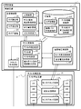
- FIG. 1 is a block diagram showing an outline of a semiconductor device 1 according to an embodiment of the present invention. Hereinafter, an outline of the semiconductor device 1 of FIG. 1 will be described.
- the semiconductor device 1 is a semiconductor device capable of detecting deterioration occurring in the test target circuit 2 (an example of “semiconductor integrated circuit” in the claims of the present application).
- the semiconductor device 1 includes a control circuit 3 that controls a test to the test target circuit 2.
- the semiconductor device 1 may include the test target circuit 2, but in the present embodiment, the test target circuit 2 and the control circuit 3 have different configurations.
- the semiconductor logic circuit is mainly a sequential circuit.
- the sequential circuit includes a combinational circuit unit 17 composed of logic elements such as an AND gate, a NAND gate, an OR gate, and a NOR gate, and a flip-flop (FF) that stores the internal state of the circuit. ).
- the test target circuit 2 includes a test unit circuit 15 which is a circuit serving as a test unit.
- the test unit circuit 15 includes a combinational circuit unit 17, a plurality of flip-flops 19 1 and 19 2, and a plurality of monitor block circuits 21 1 and 21 2 that measure frequencies (an example of “monitor block circuit” in the claims) With.
- the test unit circuit 15 may be a logical unit (block or module) handled in a logical design called a block or module, for example, or may be a logical unit (core) having a collective function.
- the core include an arithmetic operation unit, a data path unit, an IO control unit, and the like.
- the control circuit 3 controls the measurement of the temperature and voltage while changing the test operating frequency each time the test is performed, and the overall control unit 5 that controls the entire semiconductor device 1, the test control unit 7 that controls the test.
- a temperature voltage measuring unit 9 (an example of “measuring unit” in the claims of the present application), a storage unit 11 (an example of “storage unit” in the claims of the present application) for storing various information, and a clock generation circuit 13 for generating a clock; Is provided.
- the control circuit 3 is realized as a control block structure such as an overall control unit 5, a test control unit 7, and a temperature voltage measurement unit 9, and each control block is realized in a hierarchical manner as will be described below.
- the overall control unit 5 includes a main control unit 23 that controls the whole, a log reading unit 25 that reads a log, a log writing unit 27 that writes to a log, a log compression unit 29 that compresses a log, and a predetermined temperature and voltage.
- a test operation frequency conversion unit 31 that converts the test operation frequency under conditions to test operation frequencies under different temperature and voltage conditions, a deterioration amount calculation unit 33 that calculates a deterioration amount, and a deterioration determination unit 35 that determines deterioration. .
- test operation frequency conversion unit 31 is, for example, according to an approximate expression (1) described later.
- the maximum test operation frequency at the reference temperature and the reference voltage is calculated using the measured values of temperature and voltage and the maximum test operation frequency determined by the test control unit 7.
- the deterioration amount calculation unit 33 calculates a deterioration amount representing a deterioration state based on the value calculated by the test operation frequency conversion unit 31 as the maximum test operation frequency at the reference temperature and the reference voltage.
- the test control unit 7 includes a test content determination unit 37 that determines the test content for the test unit circuit 15, a test unit 39 that performs a test, and the test content within the allowable test timing for the test unit circuit 15 at each test operating frequency.
- a test discriminating unit 41 that discriminates whether or not the test content is to be executed, and a maximum test operating frequency determining unit 43 that determines the maximum test operating frequency at which the test content is executed within an allowable test timing .
- a combination of the test discriminating unit 41 and the maximum test operating frequency determining unit 43 is an example of “determining means” in the claims of the present application.
- the temperature voltage measurement unit 9 includes a monitor measurement control unit 45 that controls the measurement of the frequency of the test unit circuit 15, and a temperature voltage calculation unit 47 that estimates the temperature and voltage from the measured frequency by calculation (see “Estimation of Claims”). An example).
- “measurement” of temperature and voltage means that the temperature voltage calculation unit 47 calculates the temperature and voltage based on the measured test operation frequency.
- “measured values” of temperature and voltage refer to the values thus calculated.
- the storage unit 11 stores a log storage unit 49 that stores a log, a logical path characteristic storage unit 51 that stores a logical path characteristic, a test information storage unit 53 that stores test information, and a correction value of the test operating frequency. And a test operating frequency correction value storage unit 55.
- the overall control unit 5 transmits, for example, a test start instruction, a previous test content, an initial value of the test operation frequency F c or a current maximum test operation frequency correction value to the test control unit 7.
- the test control unit 7 sends, for example, the test unit name, the test result in the machine cycle determined at the design stage, the current maximum test operating frequency F MAX , the current test content, the temperature or the voltage to the overall control unit 5.
- the overall control unit 5 transmits log information to and from the storage unit 11.
- test control unit 7 transmits, for example, a temperature or voltage measurement start or end instruction to the temperature voltage measurement unit 9.
- the temperature voltage measuring unit 9 transmits a measured value of temperature or voltage to the test control unit 7.
- test control unit 7 transmits, for example, a test order or a final F MAX correction value to the storage unit 11.
- the storage unit 11 transmits, for example, test information to the test control unit 7.
- test control unit 7 controls the clock generation circuit 13 to generate F c , and the clock generation circuit 13 performs writing to the FFs 19 1 and 19 2 with the test clock, and then the test operation frequency F c ( Alternatively, the test pattern transmitted to the combinational circuit unit 17 is taken into the FF 19 1 or 19 2 with a clock generated at a test timing (an example of “allowable test timing” in the claims of the present application) that is the reciprocal of F c .
- the fetched test response is read from the FF 19 1 or 19 2 with a test clock and transmitted to the test control unit 7. Further, the test control unit 7 transmits a test pattern to the test target circuit 2. On the other hand, the test target circuit 2 transmits a test response to the test control unit 7.
- the temperature voltage measuring unit 9 transmits an instruction to start or end frequency measurement to the monitor block circuits 21 1 and 21 2 .
- the monitor block circuits 21 1 and 21 2 transmit the measured frequency to the temperature voltage measuring unit 9.
- FIG. 2 is a flowchart showing an outline of the design flow of the test target circuit 2 using the semiconductor device 1.
- the design flow in FIG. 2 is divided into processing up to shipment of chips (steps ST001 to ST009), processing up to shipment of the system (steps ST010 and ST011), and processing after shipment of the system (step ST012).
- a manufacturing test step ST008
- a board / system test step ST010
- a field test step ST012
- step ST001 The logic design of the test target circuit 2 is performed (step ST001), the design for testability (DFT) is performed, and the control circuit 3 and the monitor block circuits 21 1 and 21 2 are added (step ST002).
- layout design is performed (step ST003), automatic test pattern generation (ATPG) is performed, and a BIST seed pattern (test seed) is generated (step ST004).
- a logical path characteristic is acquired (step ST005). Specifically, simulation calculation of the temperature T and voltage V characteristics of the longest logical path to be tested for each test unit is performed.
- the coefficient of the approximate expression that approximates the characteristic of the relationship between the test operating frequency and the temperature and voltage is obtained.
- the inventor has found that the linearity of the frequency with respect to the temperature and voltage is good in the operating temperature range of the LSI. Therefore, the coefficients a, b, c, d, and e of the approximate expression represented by Expression (1) using the temperature T and the voltage V as variables are obtained.
- the following formula derived from the formula (1) is used.
- a mask is generated (step ST006), and a chip is manufactured (step ST007).
- a manufacturing test is performed (step ST008).
- the chip is shipped (step ST009).
- the shipped chip is combined with other chips and tested as a board or system (step ST010).
- the test unit 39 performs the first test to obtain the first (before deterioration) F MAX value, and the log writing unit 27 writes the F MAX value in the storage unit 11. Subsequently, the system is shipped (step ST011).
- a field test is performed using a free time (for example, a time other than the system operating time) (step ST012). This field test is generally performed for each test unit circuit 15. This is because the frequency varies depending on the test unit circuit 15 and the diagnostic resolution is maintained.
- step ST012 in FIG. 2 a specific example of the field test in step ST012 in FIG. 2 will be described with reference to FIG.
- a power on / off test performed at the time of system start / end will be described.
- log reading unit 25 reads the previous test contents from log storage unit 49.
- the overall control unit 5 transmits the previous test content to the test control unit 7, and the test content determination unit 37 determines the test content determined at the previous power on / off test as the current test content (step ST101).
- the test unit 39 performs a test in the machine cycle F org + ⁇ determined in the design stage, in which the operation is guaranteed.
- the temperature voltage measuring unit 9 causes the monitor block circuits 21 1 and 21 2 to measure the initial temperature (T 0 ) and the initial voltage (V 0 ) during the test.
- ⁇ is the minimum operation margin (step ST102).
- the test determination unit 41 determines whether or not the test at F org + ⁇ is passed (step ST103). If it does not move in the test at this stage, the test unit 39 performs error processing (step ST104) and ends the flow. If the test is passed, subsequently, the log reading unit 25 reads the previous F MAX at the reference temperature (T TYP ) and the reference voltage (V TYP ) from the log. Further, the test operating frequency conversion unit 31 calculates a correction value for the previous F MAX at the current conditions T 0 and V 0 to obtain the test operating frequency (F c ) (step ST105). This F c is the first maximum test operating frequency candidate in this test.
- the purpose is to reduce the number of tests by starting from the previous F MAX .
- a correction value is calculated. If the temperature condition and voltage condition of this test are the same as those of the previous test, it is not necessary to calculate a correction value in step ST105.
- the test unit 39 performs a test at the obtained test operating frequency F c , and the temperature / voltage measurement unit 9 supplies the monitor block circuits 21 1 and 21 2 with the temperature (T c ) and voltage (V c ) during the test. Measurement is performed (step ST106).
- the test determination unit 41 performs determination of whether or not pass the test at F c (step ST 107). If the test here is passed, then the test unit 39 increases the test operating frequency F c to set F c + ⁇ F 1 as a new F c (step ST108), returns to step ST106, and tests again with F c . I do. This is repeated until the test fails.
- step ST107 If it is unlikely that the performance will be improved over the previous test, measurement error is the main cause of passing at a higher test operating frequency than during the previous test. Even if the repetition is performed here, the error ⁇ F 1 is designed so that the repetition is only one time. If the test is not passed in step ST107, the process proceeds to step ST109.
- step ST109 a decrease due to deterioration of the maximum test operating frequency is obtained.
- the test unit 39 performs a test using F c ⁇ F 2 as a new F c . Further, the temperature voltage measuring unit 9 causes the monitor block circuits 21 1 and 21 2 to measure the temperature (T c ) and voltage (V c ) at the time of the test. Subsequently, the test determination unit 41 performs determination of whether or not pass the test at F c (step ST110). If passed the test herein, the F c -.DELTA.f 2 again returns to step ST109 and the new F c, repeated until the test passes. If the test is passed, the process proceeds to step ST111.
- step ST111 the maximum test operation frequency determination unit 43 determines the current F MAX the F c, the test control unit 7 transmits the time F MAX and this test content to the overall controller 5. Further, the log writing unit 27 writes F MAX at T c and V c of this test in the log. Further, the test operation frequency conversion unit 31 converts F MAX into test operation frequencies F MAX @T TYP and V TYP at the reference temperature (T TYP ) and the reference voltage (V TYP ), and the log writing unit 27 writes the log to the log. .
- the deterioration amount calculation unit 33 calculates the current deterioration amount in light of the past history of the log, and performs a calculation to subtract the allowable deterioration amount threshold value from the calculated deterioration amount (step ST112). Subsequently, the test determination unit 41 determines whether or not the obtained value is positive (step ST113). If the obtained value is not a positive value, the log compressing unit 29 compresses the log (step ST114) and ends the flow. On the other hand, if the obtained value is a positive value, the test unit 39 performs an error process (step ST115) and ends the flow.
- the deterioration determination unit 35 determines deterioration due to a single error or whether deterioration is determined when an error continues continuously in several field tests.
- the test unit 39 performs processing for the next test. Specifically, determination of the next test content, reading of the test pattern from the storage unit 11, and the like are performed.
- FIG. 4 is a diagram illustrating an example of a configuration of log information stored in the log storage unit 49.
- the log is used to efficiently measure the maximum frequency as a history of measured values and the like. Further, it is also used as a past history in order to perform an operation for statistically analyzing and removing random noise of measurement from the maximum test operating frequency in each of a plurality of tests for which deterioration determination is performed. Random noise here refers to, for example, a rounding error associated with measurement. Furthermore, the log is used to feed back and use the deterioration history in the field to design and manufacturing.
- the log information includes, for example, measurement raw data and processing information for reducing the overhead of each process.
- test time test unit (core name, etc.), test content, maximum test operating frequency (F MAX ), test temperature (T c ), test voltage ( V c ), a reference temperature and a maximum test operating frequency converted to a reference voltage (F MAX @T TYP , V TYP ) and the like.
- F MAX maximum test operating frequency
- T c test temperature
- V c test voltage
- F MAX @T TYP V TYP
- the test time is included mainly for analysis purposes, and is not essential information for the deterioration detection flow according to the embodiment of the present invention.
- the maximum test frequency is converted into the reference temperature and the reference voltage for the comparison process of each test.
- the reference temperature may be 27 ° C., for example. If there is a margin in the test time, F MAX @T TYP and V TYP may be calculated from the previous F MAX in each test instead of putting F MAX @T TYP and V TYP in the log.
- the log compression unit 29 compresses the logs in order to compress information.
- the old information is unnecessary for the deterioration determination and can be deleted. Therefore, for example, if F MAX @T TYP and V TYP are the same as the previous test, the log may be accumulated only when a change occurs without being accumulated. When there is no change, it is possible to reduce the amount of data by writing only that there is no change.
- the clock generation circuit 13 can compress the test timing by shifting a specific clock of the test clock by a specified width while keeping the clock of the reference external clock.
- FIG. 5 is a diagram showing an example of a circuit diagram of the monitor block circuits 21 1 and 21 2 .
- the monitor block circuit 21 1 includes a FF57 for holding the value, the ring oscillator (RO) 59 which oscillates in response to temperature and voltage, and a counter 61 for measuring the number of oscillations of RO59 .
- the monitor block circuit 21 1 measures the number of oscillations within a designated time (an integer multiple of the clock of Forg ), and outputs the measurement frequency measured by the counter 61.
- the monitor block circuit 21 1 In order to reduce variation in measurement frequency, not only the monitor block circuit 21 1 but also the monitor block circuit 21 2 having the same configuration is mounted on the test unit circuit 15, and RO59 provided in each of the monitor block circuits 21 1 and 21 2. The number of steps should be increased.
- the RO59 circuit is not limited to a NAND circuit or a NOT circuit.
- by adding a power cut circuit 63 cuts the power when not in use for each monitor block circuit 21 1 and 21 2, when the monitor block circuit 21 1 and 21 2 are unused RO59 Can be prevented.
- ⁇ F i (F i + ⁇ F i ) ⁇ (F i0 + ⁇ F i0 )
- ⁇ F i ⁇ F i0 is used to estimate the values of the temperature T and voltage V of the detection target circuit unit.
- FIG. 6 is a diagram illustrating an example of frequency characteristics with respect to the temperature of the RO 59.
- the three types of ring oscillators RO 1 , RO 2 and RO 3 have different rates of change with respect to changes in frequency and voltage.
- the temperature T and the voltage V are estimated from the frequency measurement values of the plurality of ROs 59 using, for example, the following expression (2).
- a 1 , b 1 , c 1 , d 1 , e 1, etc. are known parameters determined for each RO, and in step ST005 of FIG. 2, for example, simulation is performed using a technique such as multiple regression analysis. It has been demanded.
- F 1 , F 2 , and F 3 are frequencies measured in each RO.
- the temperature T c and the voltage V c at the time of the test can be obtained from the equation (2).
- the equations (1) and (2) are approximated by, for example, using piecewise functions (ie, determining coefficients by dividing ranges of temperature and voltage). The accuracy may be increased.
- the formula (2-1) is obtained from the formulas F 1 and F 2 of the formula (2).
- the formula (2-2) is obtained from the formulas F 2 and F 3 in the formula (2). That is, it can be expressed as in Expression (2-3).
- Expression (2-4) can be realized.
- the temperature T and the voltage V are expressed by Expression (2-5). That is, the temperature T and the voltage V are approximated by a linear expression of the measurement frequency F i .
- the expression (eq1) represents the expression (2-5) as a general expression.
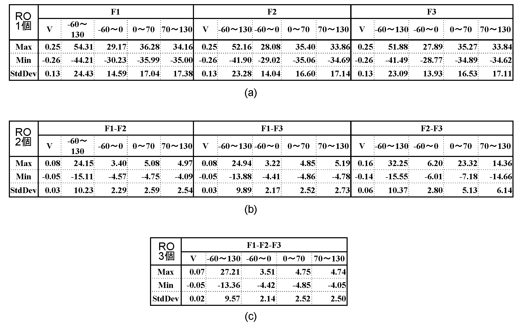
- Table 1 shows the simulation results of determining the coefficients using a plurality of RO59.
- Table 1 (a) shows the simulation results when one RO is used.
- Table 1 (b) shows the simulation results when two ROs are used.
- Table 1 (c) shows the simulation results when three ROs are used.
- the numbers in the table indicate the maximum value (Max), the minimum value (Min), and the standard deviation (StdDev) of the estimated temperature or voltage value deviation. It can be seen that the shift is much smaller when two ROs are used than when only one RO is used. For example, the standard deviation of the temperature deviation in the case of one RO is 24.43, whereas the standard deviation of the temperature deviation in the case of two ROs is 9.89 at the minimum. It is also shown that the shift is further reduced when three ROs are used.
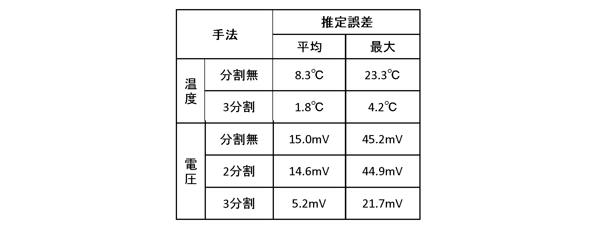
- Table 2 shows the simulation results in which the temperature range is divided for each of temperature and voltage and the coefficient of the estimation formula is determined. It can be seen that the estimation error is markedly smaller when the temperature range is divided into a plurality of ranges and the temperature and voltage are estimated, compared to when the temperature range is not divided. For example, the deviation of the average value of the estimated temperature values was 8.3 ° C. to 1.8 ° C., which was 1 ⁇ 4 or less. Moreover, the deviation of the average value of the estimated value of the voltage was about 1/3 when it was divided into 3 from 15.0 mV to 5.2 mV.
- Table 1 also shows the simulation results when the temperature is divided into three in the range of minus 60 ° C. to 130 ° C.
- the first term of equation (6) is the measured value F MAX @T C , V C , and F MAX @T TYP , V TYP is obtained by calculating the second term, the third term, and the fourth term. Can do. Usually, the second term of equation (6) is so small that it can be ignored. Eventually, as shown in equation (6-2), the maximum test frequency at the temperature and voltage during the test is expressed by a linear equation of the temperature and voltage increments. Therefore, highly accurate conversion is possible by designing a program or circuit that performs extremely simple processing.
- the deterioration amount calculation in step ST112 of FIG. 3 will be described.
- the deterioration amount is calculated based on the same test unit circuit 15 and the same test content. Since the amount of deterioration measured each time includes a random measurement error (1/2 of the measurement resolution ⁇ ), correction is required.
- two methods will be described as examples of the correction method.
- the delay deterioration amount is equal to or greater than a certain threshold value.
- malfunction at system speed / (system speed ⁇ ) due to an unspecified cause may be determined by Expression (7).
- a test for a long path including a large number of logic elements takes time, but a large number of logic elements can be tested in one test.
- a transition fault that outputs a signal different from the expected signal can be detected by performing a short path test simultaneously with a long path test on a logic element that has not been used in a long path.
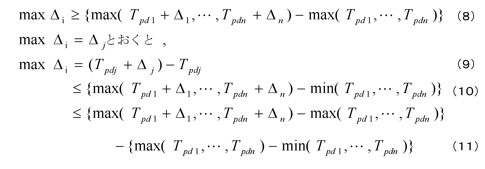
- T pd1 ,..., T pdn be the delay of the path to be tested in one test.
- max (T pd1 ,..., T pdn ) can be observed.
- the degradation amount is ⁇ i
- max (T pd1 + ⁇ 1 ,..., T pdn + ⁇ n ) can be observed. Since the path delay value ⁇ i differs for each path, the following expressions (8) to (11) hold.
- the first term of equation (11) can be observed by the difference in measured values. Therefore, if the path delay value difference in the test content, which is the second term, is reduced, the max ⁇ value can be estimated with high accuracy.
- a plurality of test contents are arranged at a plurality of levels for each length of the path to be tested.
- the first test is performed on a group of paths having a large delay (a path having a length such that the path delay T pdi satisfies T sys ⁇ 1 ⁇ T pdi ⁇ T sys ).
- T sys is the system speed.
- the second test is performed on a group of paths having the next largest delay (a path having such a length that the path delay satisfies T sys ⁇ 2 ⁇ T pdi ⁇ T sys ⁇ 1 ).
- a third test is performed on a group of paths having the next largest delay (a path having such a length that the path delay satisfies T sys ⁇ 3 ⁇ T pdi ⁇ T sys ⁇ 2 ).
- the test time is limited.
- the content of the test must be determined according to such a limited test time.
- a systematic error or the like which is a problem other than the above-described TDDB is likely to occur in a long path. Therefore, for example, if the secured test time is small by using the path length, it is assumed that the test is limited to an important element by performing a test for a long path length. That's fine.
- the secured test time is large, the device can be comprehensively tested by performing the test on a short path. As described above, it is easier to efficiently use the limited test time by performing the test on the group for each path having an appropriate length. Such efficiency improvement is particularly effective when it can be determined that TDDB is unlikely to occur due to the quality of the process.
- test time of the field test is limited to the idle time that is not used by the user. Therefore, changing the test contents and / or test order according to the allowable test timing and / or the amount of deterioration, coupled with the fact that the above-mentioned short-time test is possible, effectively causes a failure due to deterioration. It is very effective in preventing it.
- FIG. 7 is a schematic diagram illustrating an example of a test order changing method using a log history.
- the entire test set is divided into a plurality of test sets TS 1 , TS 2 ,.
- the execution order of the test list is determined as an initial test order list prepared in advance, and the test is executed while circulating in the list order according to the initial test order list.
- the test execution frequency is managed by a timer according to the progress of deterioration.
- TS 1 , TS 2 and TS 3 are executed in the first test according to the initial test order list
- 2 TS 4 , TS 5 and TS 6 are executed in the third test
- TS 7 , TS 8 and TS 1 are executed in the third test
- TS 2 , TS 3 and TS 4 are executed in the fourth test. Is done. In this way, the processes are executed in the order of the list.
- TS 1 and TS 4 are recorded and updated in the danger list based on the log history.
- TS 1 and TS 4 recorded in the danger list are preferentially executed by interrupting the initial test order list at every allowable test timing managed by the timer.
- the test execution frequency is further increased as compared to TS 4 .
- TS 1 , TS 4 and TS 2 are executed in the first test
- TS 1 , TS 3 and TS 5 are executed in the second test
- TS 1 , TS 4 and TS 6 are executed
- TS 1 , TS 7 and TS 8 are executed.
- the processes are executed in the order of the list.
- a plurality of values may be used as the test threshold value in step ST103 or step ST113 in FIG.
- two determination values may be provided for the warning level determination and the error level determination.
- an error may be output using a determination method other than the threshold determination.
- FIG. 8 is a flowchart showing an outline of another example of the field test in which the flow of FIG. 3 is partially changed.
- step ST107 the processing from step ST107 to step ST112 in the flowchart of FIG. 3 may be performed as the processing from step ST207 to step ST215 shown in FIG.
- the test determination unit 41 performs determination of whether or not pass the test at F c.
- step ST207 If the test passes in step ST207, then, the F c + ⁇ F 1 as a new F c the test unit 39 to increase the test operation frequency F c, to test. Further, the temperature voltage measuring unit 9 causes the monitor block circuits 21 1 and 21 2 to measure the temperature (T c ) and voltage (V c ) during this test (step ST208). Subsequently, the test determination unit 41 performs determination of whether or not pass the test at F c (step ST209). If the test is not passed, the maximum test operating frequency determination unit 43 determines F c ⁇ F 1 as F MAX this time.
- step ST210 T c and V c the current F MAX also a T c and V c in F c - ⁇ F 1 (step ST210), the process proceeds to step ST 214. If the test in step ST209 is passed, the process returns to step ST208 and is repeated until the test in step ST209 is not passed.
- step ST207 the test unit 39 subsequently reduces the test operating frequency F c and sets F c ⁇ F 2 as a new F c and performs a test. Further, the temperature voltage measuring unit 9 causes the monitor block circuits 21 1 and 21 2 to measure T c and V c at the time of this test (step ST211). Subsequently, the test determination unit 41 performs determination of whether or not pass the test at F c (step ST212). If the test is passed, the maximum test operating frequency determination unit 43 determines F c to be F MAX this time (step ST213), and proceeds to step ST214. If the test in step ST212 is not passed, the process returns to step ST211 and is repeated until the test in step ST212 is passed.
- the current F MAX and the current test content are transmitted from the test control unit 7 to the overall control unit 5.
- the log writing unit 27 writes F MAX at T c and V c of the current test transmitted to the log.
- the test operation frequency conversion unit 31 converts F MAX into test operation frequencies F MAX @T TYP and V TYP at the reference temperature (T TYP ) and the reference voltage (V TYP ), and the log writing unit 27 writes the log to the log. (Step ST214).
- step ST215 corresponding to step ST112
- the deterioration amount calculation unit 33 calculates the current deterioration amount in light of the past history of the log, and subtracts the allowable deterioration amount threshold value from the calculated deterioration amount. Perform the calculation.
- the processing from step ST216 to step ST218 is performed in the same manner as the processing from step ST113 to step ST115 in the flow of FIG.
- the frequency may be increased after decreasing from the previous F MAX .
- F MAX may be obtained by increasing F c in increments of ⁇ F 3 which is a smaller value of ⁇ F 2 between step ST212 and step ST213 in FIG.
- the control of the RO 59 and the control of the counter 61 may be separated. In this way, it is possible to stop the counter 61 while continuing to move the RO 59. When the oscillation of the RO 59 is stopped, the heat generation is stopped and the monitored circuit is affected. By stopping the counter 61 without exerting such an influence, it is possible to prevent an increase in circuit due to an increase in the number of bits.
- the first test is performed to obtain the first (before deterioration) F MAX value, which is stored in the storage unit included in the tester. It may be done.
- test target circuit 2 and the control circuit 3 may be separate chips as shown in FIG. 1, or the semiconductor device 1 of FIG. 1 includes the test target circuit 2, and the test target circuit 2 and the control circuit 3 are integrated. It may be realized as a thing.
- the control circuit 3 may be realized by a microcomputer or an FPGA (Field Programmable Gate Array).
- F MAX of the manufacturing test of step ST008 instead of the board / system test in step ST010 in the flow of FIG. 2, initially by testing the initial (before deterioration) The value may be obtained and the F MAX value may be written in the storage unit 11.
- RO59 instead of RO59, a circuit that functions as RO as a result of combining logic elements may be used.
- a heat sensor or a voltage sensor may be used instead of performing heat measurement and voltage measurement using the RO59.
- a general sensor requires a reference value for measurement.
- calibration before measurement and digital conversion processing after measurement are required.
- RO59 does not require a reference value for measurement.
- calibration before measurement is not necessary.
- the semiconductor device 1 can be used to detect variations occurring in a plurality of test target circuits 2 of the same type instead of detecting deterioration of the same test target circuit 2.
- the overall control unit 5 may include a difference amount calculation unit that represents the degree of variation instead of the deterioration amount calculation unit 33.
- the difference amount calculation unit calculates the difference amount based on each maximum test operation frequency obtained by the test operation frequency conversion unit 31 and obtained for a plurality of test target circuits 2 of the same type at the reference temperature and the reference voltage.
Landscapes
- Engineering & Computer Science (AREA)
- Physics & Mathematics (AREA)
- General Physics & Mathematics (AREA)
- General Engineering & Computer Science (AREA)
- Computer Hardware Design (AREA)
- Microelectronics & Electronic Packaging (AREA)
- Environmental & Geological Engineering (AREA)
- Health & Medical Sciences (AREA)
- Toxicology (AREA)
- Semiconductor Integrated Circuits (AREA)
- Tests Of Electronic Circuits (AREA)
- Testing Of Individual Semiconductor Devices (AREA)
Abstract
Description


Claims (13)
- テスト内容を実行する検知対象回路部を有する半導体集積回路に生じる劣化を検知することが可能な半導体装置であって、
前記検知対象回路部の温度及び電圧を測定する測定手段と、
各テスト動作周波数において前記検知対象回路部に対して前記テスト内容が許容テストタイミング内に実行されるか否かを判別し、実行される最大のテスト動作周波数を最大テスト動作周波数として決定する決定手段と、
前記決定手段が決定した前記最大テスト動作周波数を、前記測定手段が測定した温度及び電圧の値を用いて、基準温度及び基準電圧における最大テスト動作周波数に換算するとともに、当該換算された最大テスト動作周波数に基づき劣化の状態を表す劣化量も算出する算出手段とを備え、
前記半導体集積回路は、前記測定手段が前記温度及び電圧の値を測定するための値をモニタするモニタブロック回路を有し、
前記測定手段は、テストが行われる毎に、前記検知対象回路部の温度及び電圧の下で動作した前記モニタブロック回路がモニタした値から前記検知対象回路部の温度及び電圧の値を推定する推定手段を有し、
前記算出手段は、前記推定手段が推定した温度及び電圧の値を、前記測定手段が測定した温度及び電圧の値として用いて、前記決定手段が決定した前記最大テスト動作周波数を前記基準温度及び基準電圧における最大テスト動作周波数に換算する、半導体装置。 - 前記半導体集積回路は、n個(nは、2以上の整数)の前記モニタブロック回路を備え、
前記測定手段は、各モニタブロック回路における所定の時間内での発振回数として得られる測定周波数Fi(iは、n以下の自然数)を測定し、
前記推定手段は、式(eq1)の係数αi、β、α’i及びβ’を計算することにより、前記検知対象回路部の温度T及び電圧Vの値を推定する、請求項1記載の半導体装置。

- 前記推定手段は、温度範囲若しくは電圧範囲を複数に区分して当該区分ごとに式(eq1)の前記係数αi、β、α’i及びβ’を計算して、又は、温度範囲を複数に区分して当該区分ごとに式(eq1)の前記係数αi及びβを計算すると共に電圧範囲を複数に区分して当該区分ごとに式(eq1)の前記係数α’i及びβ’を計算することにより、前記検知対象回路部の温度T及び電圧Vの値を推定する、請求項2記載の半導体装置。
- 前記推定手段は、式(eq1)の前記測定周波数Fiに代えて、前記測定周波数Fiと初回の測定周波数Fi0との差分である差分周波数ΔFiを用いて、前記検知対象回路部の温度T及び電圧Vの値を推定する、請求項2又は3記載の半導体装置。
- 前記測定手段が測定した測定値及び前記決定手段が決定した最大テスト動作周波数の組み合わせを記憶する記憶手段をさらに備え、
前記算出手段は、前記記憶手段が記憶した測定値及び最大テスト動作周波数を用いる、請求項1から4のいずれかに記載の半導体装置。 - 前記最大テスト動作周波数は、前記記憶手段が記憶した異なるテスト時の複数の最大テスト動作周波数からランダムノイズを除去する演算が行われて決定される、請求項5記載の半導体装置。
- 前記測定手段は所定のテスト動作周波数におけるテスト時の初期温度及び初期電圧を測定し、
前記決定手段は、前記基準温度及び前記基準電圧と前回の最大テスト動作周波数とを用いながら前記初期温度及び前記初期電圧における最大テスト動作周波数候補を定め、周波数を増加後に減少させて又は増加のみ若しくは減少のみさせて、実行される最大のテスト動作周波数を最大テスト動作周波数に決定する、請求項1から6のいずれかに記載の半導体装置。 - テストされるパスの長さ毎に異なるテスト内容を用意することを特徴とする、請求項1から7のいずれかに記載の半導体装置。
- 許容テストタイミング及び/又は前記劣化量の値に応じてテスト内容及び/又はテスト順序を変更可能とする、請求項1から8のいずれかに記載の半導体装置。
- テスト内容を実行する同種の複数の半導体集積回路に生じるバラツキを検知することが可能な半導体装置であって、
前記検知対象回路部の温度及び電圧を測定する測定手段と、
各テスト動作周波数において前記検知対象回路部に対して前記テスト内容が許容テストタイミング内に実行されるか否かを判別し、実行される最大のテスト動作周波数を最大テスト動作周波数として決定する決定手段と、
前記決定手段が決定した前記最大テスト動作周波数を、前記測定手段が測定した温度及び電圧の値を用いて、基準温度及び基準電圧における最大テスト動作周波数に換算するとともに、当該換算された最大テスト動作周波数に基づきバラツキの度合を表す相違量も算出する算出手段とを備え、
前記半導体集積回路は、前記測定手段が前記温度及び電圧の値を測定するための値をモニタするモニタブロック回路を有し、
前記測定手段は、テストが行われる毎に、前記検知対象回路部の温度及び電圧の下で動作した前記モニタブロック回路がモニタした値から前記検知対象回路部の温度及び電圧の値を推定する推定手段を有し、
前記算出手段は、前記推定手段が推定した温度及び電圧の値を、前記測定手段が測定した温度及び電圧の値として用いて、前記決定手段が決定した前記最大テスト動作周波数を前記基準温度及び基準電圧における最大テスト動作周波数に換算する、半導体装置。 - 同一の半導体集積回路に生じる劣化又は同種の複数の半導体集積回路に生じるバラツキを検知することが可能な検知方法であって、
前記半導体集積回路の検知対象回路部における動作周波数と温度及び電圧との関係の特性が近似式により近似されており、
測定手段が温度及び電圧の値を測定するステップと、
決定手段が、前記半導体集積回路の検知対象回路部においてテスト内容が許容テストタイミング内に実行される最大のテスト動作周波数として最大テスト動作周波数を決定するステップと、
算出手段が、前記温度及び電圧の値並びに前記最大テスト動作周波数を用いて、前記近似式に従って基準温度及び基準電圧における最大テスト動作周波数を算出するとともに、当該算出された最大テスト動作周波数に基づき劣化の状態を表す劣化量又はバラツキの度合を表す相違量も算出するステップを含む、検知方法。 - 前記半導体集積回路は、前記測定手段が前記温度及び電圧の値を測定するための値をモニタするn個(nは、2以上の整数)のモニタブロック回路を備え、
前記測定するステップは、前記測定手段が、
各モニタブロック回路における所定の時間内での発振回数として得られる測定周波数Fi(iは、n以下の自然数)を測定する周波数測定ステップと、
式(eq2)の係数αi、β、α’i及びβ’を計算することにより、前記検知対象回路部の温度T及び電圧Vの値を推定する推定ステップとを含む、請求項11記載の検知方法。

- コンピュータに請求項11又は12に記載の検知方法を実行させるためのプログラム。
Priority Applications (5)
| Application Number | Priority Date | Filing Date | Title |
|---|---|---|---|
| CN201180014113.1A CN102812373B (zh) | 2010-03-15 | 2011-03-14 | 半导体装置、检测方法 |
| KR1020127026491A KR101746892B1 (ko) | 2010-03-15 | 2011-03-14 | 반도체 장치, 검지 방법 및 프로그램 |
| JP2012505659A JP5737524B2 (ja) | 2010-03-15 | 2011-03-14 | 半導体装置、検知方法及びプログラム |
| US13/635,057 US9316684B2 (en) | 2010-03-15 | 2011-03-14 | Semiconductor device, detection method and program |
| EP11756223.1A EP2549283A4 (en) | 2010-03-15 | 2011-03-14 | Semiconductor device, detection method, and program |
Applications Claiming Priority (2)
| Application Number | Priority Date | Filing Date | Title |
|---|---|---|---|
| JP2010057310 | 2010-03-15 | ||
| JP2010-057310 | 2010-03-15 |
Publications (1)
| Publication Number | Publication Date |
|---|---|
| WO2011115038A1 true WO2011115038A1 (ja) | 2011-09-22 |
Family
ID=44649131
Family Applications (1)
| Application Number | Title | Priority Date | Filing Date |
|---|---|---|---|
| PCT/JP2011/055900 Ceased WO2011115038A1 (ja) | 2010-03-15 | 2011-03-14 | 半導体装置、検知方法及びプログラム |
Country Status (7)
| Country | Link |
|---|---|
| US (1) | US9316684B2 (ja) |
| EP (1) | EP2549283A4 (ja) |
| JP (1) | JP5737524B2 (ja) |
| KR (1) | KR101746892B1 (ja) |
| CN (1) | CN102812373B (ja) |
| TW (1) | TW201140308A (ja) |
| WO (1) | WO2011115038A1 (ja) |
Cited By (3)
| Publication number | Priority date | Publication date | Assignee | Title |
|---|---|---|---|---|
| JP2017135131A (ja) * | 2016-01-25 | 2017-08-03 | 日立オートモティブシステムズ株式会社 | 集積回路 |
| JP2019502935A (ja) * | 2016-01-08 | 2019-01-31 | アップル インコーポレイテッドApple Inc. | 計測システムのための基準回路 |
| JP2019505997A (ja) * | 2016-01-21 | 2019-02-28 | アップル インコーポレイテッドApple Inc. | 電圧低下のデジタル検出及び制御のための方法並びに装置 |
Families Citing this family (14)
| Publication number | Priority date | Publication date | Assignee | Title |
|---|---|---|---|---|
| US9594406B2 (en) * | 2011-11-17 | 2017-03-14 | Gunze Limited | Touch panel and method for producing same |
| US10466763B2 (en) * | 2013-12-02 | 2019-11-05 | Nvidia Corporation | Dynamic voltage-frequency scaling to limit power transients |
| CN104157121B (zh) * | 2014-08-22 | 2017-01-25 | 北京机电工程研究所 | 面向无线数据传输设备的直接健康因子构建方法 |
| JP2016188825A (ja) | 2015-03-30 | 2016-11-04 | ルネサスエレクトロニクス株式会社 | 半導体装置及びシステム |
| US20170272073A1 (en) * | 2016-03-18 | 2017-09-21 | Altera Corporation | Dynamic parameter operation of an fpga |
| US10615802B2 (en) * | 2016-03-18 | 2020-04-07 | The Governing Council Of The University Of Toronto | Dynamic parameter operation of an FPGA |
| KR20180078897A (ko) * | 2016-12-30 | 2018-07-10 | 삼성전자주식회사 | 반도체 장치의 테스트 방법 및 이를 수행하는 테스트 시스템 |
| CN108535624B (zh) * | 2017-03-06 | 2020-08-07 | 中芯国际集成电路制造(上海)有限公司 | 一种集成电路芯片及其保护方法、装置 |
| EP3432014A1 (de) * | 2017-07-19 | 2019-01-23 | Siemens Aktiengesellschaft | Verfahren und system zur prädiktiven wartung von integrierten schaltungen |
| CN107727061B (zh) * | 2017-09-27 | 2021-03-09 | 武汉霸云创新科技有限公司 | 一种自主气象改正的光电测距系统及方法 |
| JP6962795B2 (ja) * | 2017-11-22 | 2021-11-05 | ルネサスエレクトロニクス株式会社 | 半導体装置および半導体システム |
| CN112526319B (zh) * | 2020-11-25 | 2022-11-22 | 海光信息技术股份有限公司 | 芯片测试方法、装置、处理器芯片及服务器 |
| CN116953466B (zh) * | 2023-09-21 | 2023-12-01 | 江苏摩派半导体有限公司 | 半导体器件环境可靠性测试方法和系统 |
| CN120801974B (zh) * | 2025-07-16 | 2026-04-24 | 深圳市美浦森半导体有限公司 | 基于数据驱动的功率半导体故障预警方法及系统 |
Citations (5)
| Publication number | Priority date | Publication date | Assignee | Title |
|---|---|---|---|---|
| JPH07191095A (ja) * | 1993-10-18 | 1995-07-28 | Tektronix Inc | タイミング・アナライザ |
| JPH0961503A (ja) * | 1995-08-21 | 1997-03-07 | Advantest Corp | 半導体試験装置における試験信号のタイミング校正装置 |
| JPH09292436A (ja) * | 1996-04-26 | 1997-11-11 | Matsushita Electric Ind Co Ltd | タイミング検証方法 |
| JP2003068865A (ja) | 2001-08-30 | 2003-03-07 | Sony Corp | 半導体デバイスの自己診断方法および装置 |
| JP2010524101A (ja) | 2007-04-10 | 2010-07-15 | インターナショナル・ビジネス・マシーンズ・コーポレーション | デジタル・システムの信頼性を監視する方法、及びそのシステム |
Family Cites Families (27)
| Publication number | Priority date | Publication date | Assignee | Title |
|---|---|---|---|---|
| US5795068A (en) * | 1996-08-30 | 1998-08-18 | Xilinx, Inc. | Method and apparatus for measuring localized temperatures and voltages on integrated circuits |
| JP3138701B2 (ja) * | 1999-03-16 | 2001-02-26 | 日本電気アイシーマイコンシステム株式会社 | 半導体集積回路のテスト方法とその装置 |
| JP2001021609A (ja) * | 1999-07-07 | 2001-01-26 | Mitsubishi Electric Corp | 半導体集積回路の検査方法 |
| JP2002009238A (ja) * | 2000-06-19 | 2002-01-11 | Matsushita Electric Ind Co Ltd | スキャンパス設計方法 |
| NZ530434A (en) * | 2001-07-02 | 2005-01-28 | Battelle Memorial Institute | Intelligent microsensor module |
| JP3798713B2 (ja) * | 2002-03-11 | 2006-07-19 | 株式会社東芝 | 半導体集積回路装置及びそのテスト方法 |
| US6737671B2 (en) * | 2002-06-26 | 2004-05-18 | Infineon Technologies Richmond, Lp | Current measurement circuit and method for voltage regulated semiconductor integrated circuit devices |
| JP3940718B2 (ja) * | 2003-10-30 | 2007-07-04 | 株式会社東芝 | 試験装置、良否判定基準設定装置、試験方法及び試験プログラム |
| JP2005172549A (ja) * | 2003-12-10 | 2005-06-30 | Matsushita Electric Ind Co Ltd | 半導体集積回路の検証方法及びテストパターンの作成方法 |
| US6900650B1 (en) | 2004-03-01 | 2005-05-31 | Transmeta Corporation | System and method for controlling temperature during burn-in |
| US7151389B2 (en) * | 2004-03-05 | 2006-12-19 | Qualitau, Inc. | Dual channel source measurement unit for semiconductor device testing |
| JP4367225B2 (ja) * | 2004-05-11 | 2009-11-18 | ソニー株式会社 | 半導体集積回路 |
| JP4198644B2 (ja) * | 2004-06-21 | 2008-12-17 | 富士通マイクロエレクトロニクス株式会社 | 半導体集積回路 |
| US7338817B2 (en) * | 2005-03-31 | 2008-03-04 | Intel Corporation | Body bias compensation for aged transistors |
| CN101313226B (zh) * | 2005-12-30 | 2013-02-13 | 英特尔公司 | 半导体器件的寿命的动态估算方法和设备 |
| TW200801550A (en) * | 2006-01-06 | 2008-01-01 | Koninkl Philips Electronics Nv | IC testing methods and apparatus |
| CN101078997A (zh) * | 2006-04-18 | 2007-11-28 | 松下电器产业株式会社 | 半导体集成电路系统、半导体集成电路、操作系统和半导体集成电路的控制 |
| US7480588B1 (en) * | 2006-04-19 | 2009-01-20 | Darryl Walker | Semiconductor device having variable parameter selection based on temperature and test method |
| WO2008000858A1 (es) * | 2006-06-30 | 2008-01-03 | Intel Corporation | Estimación de la potencia de fugas |
| US20080035921A1 (en) * | 2006-08-11 | 2008-02-14 | Christopher Gonzalez | Method and circuit for detecting and compensating for a degradation of a semiconductor device |
| JP2008066536A (ja) * | 2006-09-07 | 2008-03-21 | Toshiba Corp | 半導体集積回路 |
| WO2008038546A1 (en) * | 2006-09-26 | 2008-04-03 | Panasonic Corporation | Semiconductor inspecting apparatus and semiconductor integrated circuit |
| JP4439533B2 (ja) * | 2007-03-27 | 2010-03-24 | 株式会社東芝 | 負荷算定装置および負荷算定方法 |
| JP4491002B2 (ja) * | 2007-08-31 | 2010-06-30 | 株式会社東芝 | 半導体集積回路装置 |
| US7668682B2 (en) * | 2007-10-25 | 2010-02-23 | International Business Machines Corporation | Method and circuit for detecting and compensating for a degradation of a semiconductor device |
| US8183910B2 (en) * | 2008-11-17 | 2012-05-22 | Taiwan Semiconductor Manufacturing Co., Ltd. | Circuit and method for a digital process monitor |
| US8081003B2 (en) * | 2009-02-02 | 2011-12-20 | Infineon Technologies Ag | Circuit arrangement with a test circuit and a reference circuit and corresponding method |
-
2011
- 2011-03-11 TW TW100108218A patent/TW201140308A/zh unknown
- 2011-03-14 WO PCT/JP2011/055900 patent/WO2011115038A1/ja not_active Ceased
- 2011-03-14 JP JP2012505659A patent/JP5737524B2/ja not_active Expired - Fee Related
- 2011-03-14 US US13/635,057 patent/US9316684B2/en not_active Expired - Fee Related
- 2011-03-14 KR KR1020127026491A patent/KR101746892B1/ko not_active Expired - Fee Related
- 2011-03-14 EP EP11756223.1A patent/EP2549283A4/en not_active Withdrawn
- 2011-03-14 CN CN201180014113.1A patent/CN102812373B/zh not_active Expired - Fee Related
Patent Citations (5)
| Publication number | Priority date | Publication date | Assignee | Title |
|---|---|---|---|---|
| JPH07191095A (ja) * | 1993-10-18 | 1995-07-28 | Tektronix Inc | タイミング・アナライザ |
| JPH0961503A (ja) * | 1995-08-21 | 1997-03-07 | Advantest Corp | 半導体試験装置における試験信号のタイミング校正装置 |
| JPH09292436A (ja) * | 1996-04-26 | 1997-11-11 | Matsushita Electric Ind Co Ltd | タイミング検証方法 |
| JP2003068865A (ja) | 2001-08-30 | 2003-03-07 | Sony Corp | 半導体デバイスの自己診断方法および装置 |
| JP2010524101A (ja) | 2007-04-10 | 2010-07-15 | インターナショナル・ビジネス・マシーンズ・コーポレーション | デジタル・システムの信頼性を監視する方法、及びそのシステム |
Non-Patent Citations (6)
| Title |
|---|
| O. KHAN ET AL.: "A Self-Adaptive System Architecture to Address transistor Aging", PROC. DESIGN AUTOMATION AND TEST IN EUROPE, 2009, pages 81 - 86, XP032317470, DOI: doi:10.1109/DATE.2009.5090637 |
| SATO ET AL.: "A Survey of Approaches for High Field Reliability", REAJ, vol. 31, no. 7, pages 514 - 519 |
| See also references of EP2549283A4 |
| T. VO ET AL.: "Design for Board and System Level Structure Test and Diagnosis", PROC. INTL. TEST CONF., 2006, pages 1 - 10 |
| Y. LI ET AL.: "CASP: Concurrent Autonomous Chip Self-Test Using Stored Test Patterns", PROC. DESIGN AUTOMATION AND TEST IN EUROPE, 2008, pages 885 - 890, XP031241898 |
| Y. SATO ET AL.: "A Circuit Failure Prediction Mechanism (DART) for High Field Reliability", THE 8TH IEEE INTERNATIONAL CONFERENCE ON ASIC, 2009, pages 581 - 584, XP031578952 |
Cited By (5)
| Publication number | Priority date | Publication date | Assignee | Title |
|---|---|---|---|---|
| JP2019502935A (ja) * | 2016-01-08 | 2019-01-31 | アップル インコーポレイテッドApple Inc. | 計測システムのための基準回路 |
| US10527503B2 (en) | 2016-01-08 | 2020-01-07 | Apple Inc. | Reference circuit for metrology system |
| US11022503B2 (en) | 2016-01-08 | 2021-06-01 | Apple Inc. | Reference circuit for metrology system |
| JP2019505997A (ja) * | 2016-01-21 | 2019-02-28 | アップル インコーポレイテッドApple Inc. | 電圧低下のデジタル検出及び制御のための方法並びに装置 |
| JP2017135131A (ja) * | 2016-01-25 | 2017-08-03 | 日立オートモティブシステムズ株式会社 | 集積回路 |
Also Published As
| Publication number | Publication date |
|---|---|
| EP2549283A1 (en) | 2013-01-23 |
| KR20130054248A (ko) | 2013-05-24 |
| JP5737524B2 (ja) | 2015-06-17 |
| TW201140308A (en) | 2011-11-16 |
| CN102812373B (zh) | 2014-12-10 |
| JPWO2011115038A1 (ja) | 2013-06-27 |
| US20130013247A1 (en) | 2013-01-10 |
| EP2549283A4 (en) | 2017-06-21 |
| US9316684B2 (en) | 2016-04-19 |
| KR101746892B1 (ko) | 2017-06-14 |
| CN102812373A (zh) | 2012-12-05 |
Similar Documents
| Publication | Publication Date | Title |
|---|---|---|
| JP5737524B2 (ja) | 半導体装置、検知方法及びプログラム | |
| CN111837045B (zh) | 集成电路工作负载、温度和/或亚阈值泄漏传感器 | |
| CN101669037B (zh) | 监视数字系统的可靠性 | |
| JP5382126B2 (ja) | 経年劣化診断装置、経年劣化診断方法 | |
| TWI550288B (zh) | 用於決定電路之預定物理性質之變化的設備及方法 | |
| JP5476995B2 (ja) | 半導体装置の解析方法及び調整方法と半導体システム | |
| US7668682B2 (en) | Method and circuit for detecting and compensating for a degradation of a semiconductor device | |
| US20160154055A1 (en) | On-die system for monitoring and predicting performance | |
| US8935143B2 (en) | Semiconductor sensor reliability | |
| US10288496B1 (en) | Ring oscillator for temperature or voltage sensing | |
| JP5843358B2 (ja) | 半導体集積回路のテストパターン生成方法、プログラム、およびコンピュータ読み取り可能な記録媒体 | |
| Xue et al. | A one-pass test-selection method for maximizing test coverage | |
| Zandian et al. | Wearmon: Reliability monitoring using adaptive critical path testing | |
| KR20260030941A (ko) | 예측 장치, 검사 시스템, 예측 방법 및 예측 프로그램 | |
| US20230168295A1 (en) | Circuits and techniques for predicting end of life based on in situ monitors and limit values defined for the in situ monitors | |
| JP6469598B2 (ja) | 集積回路 | |
| Wunderlich et al. | Test Aspects of System Health State Monitoring | |
| JP4705493B2 (ja) | 半導体集積回路 | |
| RU2397504C1 (ru) | Способ диагностического неразрушающего контроля (днк) программируемых логических интегральных схем иностранного производства (плис ип) | |
| Chung et al. | Defect Diagnosis via Segment Delay Learning | |
| JPWO2009066764A1 (ja) | 半導体集積回路装置及びそのテスト方法 | |
| JP2006250863A (ja) | 半導体試験方法及び半導体装置 | |
| JP2012154809A (ja) | モニタリング装置及びモニタリングシステム |
Legal Events
| Date | Code | Title | Description |
|---|---|---|---|
| WWE | Wipo information: entry into national phase |
Ref document number: 201180014113.1 Country of ref document: CN |
|
| 121 | Ep: the epo has been informed by wipo that ep was designated in this application |
Ref document number: 11756223 Country of ref document: EP Kind code of ref document: A1 |
|
| WWE | Wipo information: entry into national phase |
Ref document number: 13635057 Country of ref document: US Ref document number: 2012505659 Country of ref document: JP |
|
| NENP | Non-entry into the national phase |
Ref country code: DE |
|
| ENP | Entry into the national phase |
Ref document number: 20127026491 Country of ref document: KR Kind code of ref document: A |
|
| WWE | Wipo information: entry into national phase |
Ref document number: 2011756223 Country of ref document: EP |