WO2011115074A1 - コンタクトプローブおよびプローブユニット - Google Patents
コンタクトプローブおよびプローブユニット Download PDFInfo
- Publication number
- WO2011115074A1 WO2011115074A1 PCT/JP2011/055969 JP2011055969W WO2011115074A1 WO 2011115074 A1 WO2011115074 A1 WO 2011115074A1 JP 2011055969 W JP2011055969 W JP 2011055969W WO 2011115074 A1 WO2011115074 A1 WO 2011115074A1
- Authority
- WO
- WIPO (PCT)
- Prior art keywords
- contact
- probe
- contact portion
- elastic
- arc shape
- Prior art date
- Legal status (The legal status is an assumption and is not a legal conclusion. Google has not performed a legal analysis and makes no representation as to the accuracy of the status listed.)
- Ceased
Links
Images






Classifications
-
- G—PHYSICS
- G01—MEASURING; TESTING
- G01R—MEASURING ELECTRIC VARIABLES; MEASURING MAGNETIC VARIABLES
- G01R1/00—Details of instruments or arrangements of the types included in groups G01R5/00 - G01R13/00 and G01R31/00
- G01R1/02—General constructional details
- G01R1/06—Measuring leads; Measuring probes
- G01R1/067—Measuring probes
-
- G—PHYSICS
- G01—MEASURING; TESTING
- G01R—MEASURING ELECTRIC VARIABLES; MEASURING MAGNETIC VARIABLES
- G01R1/00—Details of instruments or arrangements of the types included in groups G01R5/00 - G01R13/00 and G01R31/00
- G01R1/02—General constructional details
- G01R1/04—Housings; Supporting members; Arrangements of terminals
- G01R1/0408—Test fixtures or contact fields; Connectors or connecting adaptors; Test clips; Test sockets
- G01R1/0433—Sockets for IC's or transistors
- G01R1/0441—Details
- G01R1/0466—Details concerning contact pieces or mechanical details, e.g. hinges or cams; Shielding
-
- H—ELECTRICITY
- H01—ELECTRIC ELEMENTS
- H01R—ELECTRICALLY-CONDUCTIVE CONNECTIONS; STRUCTURAL ASSOCIATIONS OF A PLURALITY OF MUTUALLY-INSULATED ELECTRICAL CONNECTING ELEMENTS; COUPLING DEVICES; CURRENT COLLECTORS
- H01R13/00—Details of coupling devices of the kinds covered by groups H01R12/70 or H01R24/00 - H01R33/00
- H01R13/02—Contact members
- H01R13/22—Contacts for co-operating by abutting
- H01R13/24—Contacts for co-operating by abutting resilient; resiliently-mounted
- H01R13/2435—Contacts for co-operating by abutting resilient; resiliently-mounted with opposite contact points, e.g. C beam
-
- H—ELECTRICITY
- H01—ELECTRIC ELEMENTS
- H01R—ELECTRICALLY-CONDUCTIVE CONNECTIONS; STRUCTURAL ASSOCIATIONS OF A PLURALITY OF MUTUALLY-INSULATED ELECTRICAL CONNECTING ELEMENTS; COUPLING DEVICES; CURRENT COLLECTORS
- H01R13/00—Details of coupling devices of the kinds covered by groups H01R12/70 or H01R24/00 - H01R33/00
- H01R13/02—Contact members
- H01R13/22—Contacts for co-operating by abutting
- H01R13/24—Contacts for co-operating by abutting resilient; resiliently-mounted
- H01R13/2442—Contacts for co-operating by abutting resilient; resiliently-mounted with a single cantilevered beam
Definitions
- the present invention relates to a contact probe and a probe unit used for connection between electric circuit boards and the like.
- an electrical connection is made between the inspection target and a signal processing device that outputs an inspection signal.
- a probe unit that accommodates a plurality of conductive contact probes is used.
- the probe unit can be applied to highly integrated and miniaturized inspection objects by narrowing the pitch between contact probes with the progress of high integration and miniaturization of semiconductor integrated circuits and liquid crystal panels in recent years. Possible technologies are progressing.
- Patent Document 1 discloses a probe unit in which contact probes each having a spring shape and curved in contact with a contact body are accommodated in a test board. This contact probe has a spring portion in common with the electrical signal conducting portion.
- the present invention has been made in view of the above, and an object of the present invention is to provide a contact probe and a probe unit that have a spring property and can obtain reliable and good conduction between contact objects.
- a contact probe according to the present invention is a substantially flat contact probe having a uniform plate thickness for connecting different substrates, and has a side surface curved in an arc.
- the first contact portion that contacts one substrate at the side surface
- the second contact portion that contacts the other substrate at the side surface
- the second contact portion that contacts the other substrate at the side surface, the first contact portion, and the second contact surface.
- a connecting portion that connects the contact portion, an elastic portion that extends from the second contact portion, is partially curved in an arc shape, and is elastically deformed by a load applied to the first contact portion and the second contact portion; , Provided.
- the contact probe according to the present invention is characterized in that, in the above invention, the width of the elastic portion is smaller than the width of the connection portion.
- the contact probe according to the present invention is characterized in that, in the above invention, the connection portion has an arc shape.
- the contact probe according to the present invention is characterized in that, in the above invention, a part of the elastic portion is linear.
- the elastic portion includes a first plane in contact with the first contact portion, a parallel to the first plane, and the second contact portion. It is located between the 2nd planes which touch.
- the probe unit according to the present invention has a side surface curved in an arc shape, and has a first contact portion that contacts one substrate at the side surface, a side surface curved in an arc shape, and the other substrate at the side surface.
- a second contact portion that contacts, a connection portion that connects the first contact portion and the second contact portion, a shape that extends from the second contact portion and is partially curved in an arc shape, and the first contact
- an elastic part that is elastically deformed by a load applied to the second contact part, and a substantially flat contact probe having a holding part that holds the contact probe.
- the holding portion has a diameter equal to that of the elastic portion, and receives and fixes an end portion different from the connection portion side of the elastic portion. Is provided.
- the probe unit according to the present invention is characterized in that, in the above-described invention, the holding portion is in contact with the second contact portion at least at one place.
- the second contact portion is a contact that is the shortest among contact portions that are in contact with the other substrate and the holding portion in a state where no load is applied.
- An outer edge connecting the portions has an R shape.
- the probe unit according to the present invention is characterized in that, in the above invention, the holding portion is formed with a slit capable of accommodating the contact probe.
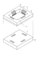
- FIG. 1 is a perspective view showing the configuration of the probe unit according to the first embodiment of the present invention.
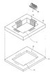
- FIG. 2 is an exploded perspective view showing a configuration of a main part of the probe unit shown in FIG.
- FIG. 3 is an exploded perspective view showing a configuration of a main part of the probe unit shown in FIG.
- FIG. 4 is a perspective view showing a configuration of a main part of the probe unit shown in FIG.
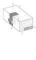
- FIG. 5 is a perspective view showing the contact probe according to the first embodiment of the present invention.
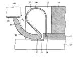
- FIG. 6 is a partial cross-sectional view showing a configuration of a main part of the probe unit shown in FIG.
- FIG. 7 is a partial cross-sectional view showing a configuration of a main part of the probe unit shown in FIG. FIG.
- FIG. 8 is a partial cross-sectional view showing a configuration of a main part of the probe unit shown in FIG.
- FIG. 9 is a perspective view showing a contact probe which is a first modification of the first embodiment of the present invention.
- FIG. 10 is a perspective view showing a contact probe which is a second modification of the first embodiment of the present invention.
- FIG. 11 is a perspective view showing a contact probe which is a third modification of the first embodiment of the present invention.
- FIG. 12 is a perspective view showing a contact probe that is a fourth modification of the first embodiment of the present invention.
- FIG. 13 is a perspective view showing a contact probe which is a fifth modification of the first embodiment of the present invention.
- FIG. 14 is a perspective view showing a contact probe according to Embodiment 2 of the present invention.
- FIG. 15 is a partial cross-sectional view showing the configuration of the main part of the probe unit according to the second embodiment of the present invention.
- FIG. 16 is a partial cross-sectional view showing the configuration of the main part of the probe unit according to the second embodiment of the present invention.
- FIG. 17 is a perspective view showing a semiconductor integrated circuit which is a modification of the embodiment of the present invention.
- FIG. 1 is a perspective view showing the configuration of the probe unit according to the first embodiment of the present invention.
- a probe unit 1 shown in FIG. 1 is a device that is used when an electrical characteristic test is performed on a semiconductor integrated circuit 100 that is an object to be tested, and a circuit that outputs a test signal to the semiconductor integrated circuit 100 and the semiconductor integrated circuit 100.
- This is an apparatus for electrically connecting the substrate 30.
- the semiconductor integrated circuit 100 is described as being a QFN (Quad Flat Non-Leaded Package) having the electrode 101.
- the probe unit 1 includes a conductive contact probe 20 (hereinafter simply referred to as a “probe 20”) that contacts two different contact objects, ie, a semiconductor integrated circuit 100 and a circuit board 30, and a plurality of probes 20 in a predetermined pattern. And a circuit board 30 that contacts the bottom of the probe holder 10 and outputs a test signal to the semiconductor integrated circuit 100 via the probe 20.
- a conductive contact probe 20 hereinafter simply referred to as a “probe 20”
- a circuit board 30 that contacts the bottom of the probe holder 10 and outputs a test signal to the semiconductor integrated circuit 100 via the probe 20.
- the circuit board 30 has an electrode 31 for outputting a test signal to the semiconductor integrated circuit 100 via the probe 20 as shown in FIG.
- the electrode 31 is disposed on the circuit board 30 corresponding to the probe 20 held by the probe holder 10.
- the probe holder 10 and the circuit board 30 may be connected by screws or the like, or may be bonded by an adhesive or a seal member. Any bonding form is possible as long as the contact between the probe 20 and the electrode 31 is not hindered.
- the probe holder 10 is formed using an insulating material, and includes a housing portion 11 in which a housing space capable of housing the semiconductor integrated circuit 100 is formed, and a slit 12 for holding the probe 20 in a predetermined pattern.
- the slit 12 holds the probe 20 so that the tip of the probe 20 protrudes toward the accommodating portion 11 side. Further, when the semiconductor integrated circuit 100 is accommodated in the accommodating portion 11, the slit 12 is formed at a position where each probe 20 contacts the electrode 101 of the corresponding semiconductor integrated circuit 100.
- FIG. 3 is an exploded perspective view showing a configuration of a main part of the probe unit 1 shown in FIG.
- FIG. 4 is a perspective view showing a configuration of a main part of the probe unit 1 shown in FIG.
- the probe holder 10 is configured by detachably connecting a fixing member 13 that fixes the probe 20 to the outer periphery of the bottom.
- the fixing member 13 is formed using an insulating material, and includes an opening 15 that is larger than the probe holder 10 and a hole 14 that holds and fixes the probe 20.
- the probe holder 10 has a rectangular parallelepiped shape by fitting with the fixing member 13 at a notch corresponding to the fixing member 13 and constitutes a holding portion that holds the probe 20.
- the hole portion 14 accommodates the end portion of the probe 20 inserted through the slit 12, and holds the probe 20 so that the other tip portion of the probe 20 is positioned at a predetermined position of the accommodation portion 11. If the probe 20 can be fixed at a predetermined interval and in a predetermined direction, the holding portion may be configured only by the fixing member 13, and the probe unit 10 and the hole portion 14 of the fixing member 13 are integrally formed. Also good.
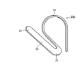
- FIG. 5 is a perspective view showing the probe 20 according to the first embodiment of the present invention.
- 6 is a cross-sectional view taken along a plane passing through the center of the slit 12 shown in FIG.
- the probe 20 shown in FIGS. 5 and 6 has a substantially flat plate shape with a uniform plate thickness, and has a side surface curved in an arc shape at the tip, and a first contact portion 21 that contacts the semiconductor integrated circuit 100 on this side surface.
- a second contact portion 22 having a side surface curved in an arc shape and contacting the circuit board 30 on the side surface; a strip-shaped connection portion 23 connecting the first contact portion 21 and the second contact portion 22; And an elastic part 24 that extends from the part 22 and is partially curved in an arc shape and elastically deforms by a load applied to the first contact part 21 and the second contact part 22.
- the probe 20 is formed using an alloy such as copper, nickel, iron, or tungsten.
- molding using the material which has elasticity, what gave the plating process to the surface may be used.
- the side surface of the second contact portion 22 that is curved in an arc shape is held by the probe holder 10 and contacts the electrode 31 of the circuit board 30 as shown in the cross-sectional view of FIG.
- the elastic part 24 has a smaller width than the width of the connection part 23. For this reason, the elastic portion 24 is more likely to be elastically deformed than the other portions with respect to the load applied to the first contact portion 21 or the second contact portion 22.
- the ratio between the width of the elastic part 24 and the width of the connecting part 23 may be any ratio as long as the elastic part 24 can be preferentially elastically deformed.
- the end portion of the elastic portion 24 in a direction different from the second contact portion 22 extends in a straight line shape, and the tip portion of the straight line portion is inserted and attached to the hole portion 14 so that the probe 20 is attached to the probe holder. 10 is held.
- FIG. 7 is a partial cross-sectional view showing a state in which a load is applied to the first contact portion 21 or the second contact portion 22.
- FIG. 7 when the first contact portion 21 contacts the electrode 101 of the semiconductor integrated circuit 100 and a load is applied in the direction of the arrow in the figure, the curved portion of the elastic portion 24 is elastically deformed.
- broken lines P 0 indicates the position of the probe 20 in a state where no load is applied as shown in FIG.
- the first contact portion 21 and the second contact portion 22 are not elastically deformed and contact the electrodes 101 and 31 according to the load. Move while touching. Further, the elastic portion 24 undergoes elastic deformation in accordance with a load transmitted via the connection portion 23 and the second contact portion 22. Note that most of the current flowing at this time flows through the first contact portion 21, the connection portion 23, and the second contact portion 22.
- FIG. 8 is a diagram for explaining a contact state between the first contact portion 21 and the electrode 101 and a contact state between the second contact portion 22 and the electrode 31 before and after a load is applied to the first contact portion 21.
- FIG. 8A shows a state where the electrode 101 of the semiconductor integrated circuit 100 is in contact with the first contact portion 21 (a state where no load is applied).
- the contact point between the first contact portion 21 and the electrode 101 is S 0
- the contact point between the second contact portion 22 and the electrode 31 is C 0 .
- FIG. 8A when the semiconductor integrated circuit 100 moves in the direction of the arrow, a load is applied to the first contact portion 21 and the first contact portion 21 is pushed down. Due to the movement of the first contact portion 21, the contact points of the first contact portion 21 and the second contact portion 22 with the electrodes 101 and 31 are shifted to S 1 and C 1 respectively (FIG. 8B).
- the broken line P 0 indicates the position of the probe 20 in a state where no load is applied as shown in FIG. 8A, and the broken line I 0 indicates the position of the semiconductor integrated circuit 100 shown in FIG. Yes.
- each contact part 21 and the second contact portion 22 rotate on the electrodes 101 and 31, and the contact points move. For this reason, each contact part has a small frictional force applied to each electrode, and can suppress wear of the contact part and each electrode.
- the probe unit 1 according to the first embodiment described above has a different shape between the portion that conducts electricity in the same probe and the portion that has a spring property, the electrical conduction path becomes longer by securing the spring property. Therefore, it is possible to design the probe without fail, to ensure reliable electrical conduction and to ensure the spring property of the probe. Moreover, since each contact part rotates with respect to a contact with an electrode and moves a contact, the friction between a contact part and an electrode can be reduced and abrasion of a contact part and an electrode can be suppressed.
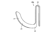
- FIG. 9 is a perspective view showing a probe 20a that is a first modification of the first embodiment.
- the probe 20 a includes the first contact portion 21 and the second contact portion 22 described above, a connection portion 23 that connects the first contact portion 21 and the second contact portion 22, and a part of the probe 20 a in an arc shape. And an elastic portion 25 that is elastically deformed by a load applied to the first contact portion 21 and the second contact portion 22.
- the elastic portion 25 is formed to be curved so that the straight portions on both ends are parallel. Further, the radius of curvature of the curved portion of the elastic portion 25 is smaller than the radius of curvature of the elastic portion 24 shown in FIG. Note that the width of the elastic portion 25 is smaller than the width of the connecting portion 23.
- the probe 20a described above is effective when the device is downsized because the curved portion of the elastic portion 25 is small.
- the contact direction between the probe 20 and the semiconductor integrated circuit 100 is as shown in FIGS. 7 and 8, the formation region of the curved portion of the elastic portion 25 is connected to the moving direction of the semiconductor integrated circuit 100. Since the region where the portion 23 is formed does not overlap, the probe can be further downsized by shortening the connecting portion 23.
- FIG. 10 is a perspective view showing a probe 20b that is a second modification of the first embodiment.
- the probe 20 b includes the first contact portion 21 and the second contact portion 22 described above, a linear connection portion 26 that connects the first contact portion 21 and the second contact portion 22, and An elastic part 24 that is partially curved in an arc shape and elastically deforms by a load applied to the first contact part 21 and the second contact part 22 is provided.
- the probe 20b has the same effect as that of the first embodiment described above, and the radius of curvature of the contact portion of the second contact portion 22 with the electrode is small and the distance to rotate on the electrode is shortened. Useful when the size is small. Further, since the connection portion 26 has a shorter conduction distance than the arc-shaped connection portion 23, it is possible to obtain more stable conduction.
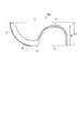
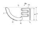
- FIG. 11 is a perspective view showing a probe 20c that is a third modification of the first embodiment.
- the probe 20 c includes the first contact portion 21 and the second contact portion 22 described above, a connection portion 23 that connects the first contact portion 21 and the second contact portion 22, and a second contact portion.
- an elastic portion 27 that extends from 22 and is partially curved in an arc shape and elastically deforms by a load applied to the first contact portion 21 and the second contact portion 22. Note that the width of the elastic portion 27 is smaller than the width of the connecting portion 23.
- the elastic portion 27 is positioned between the first plane G 1 that is in contact with the first contact portion 21 and the second plane G 2 that is parallel to the first plane G 1 and is in contact with the second contact portion 22. To do. That is, the elastic portion 27, the second plane G 2, the distance d2 to the farthest point in the second plane G 2 of the elastic portion 27, the first plane G 1 and the second plane G 2 It is curved and formed to be smaller than the distance d1 between them.
- the probe 20c has the same effect as that of the first embodiment described above. For example, when the probe 20c is held by the probe holder 1 to perform inspection, the semiconductor integrated circuit 100 from above in the region including the region where the elastic portion 27 is formed. Even when the two approaches, the elastic part 27 and the semiconductor integrated circuit 100 can be inspected without contact.
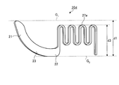
- a probe 20d having an elastic portion 27a having a shape that extends in a zigzag shape by repeating curved portions having opposite concavities and convexities may be used.
- Elastic portion 27a is reciprocally in a direction substantially orthogonal to the plane G 1, G 2, a shape extending in a direction parallel to the plane G 1, G 2.
- the second plane G 2 the distance d3 to the second point farthest to the plane G 2 of the resilient portion 27a, the distance between the first plane G 1 and the second plane G 2 It is curved and formed so as to be smaller than d1.
- a probe 20e having an elastic portion 27b having a shape that extends in a zigzag shape by repeating curved portions having opposite concavities and convexities may be used.
- Elastic portion 27b is to reciprocate in a direction parallel to the plane G 1, G 2, a shape extending in the plane G 1, G 2 and perpendicular.
- the second plane G 2 the distance d4 to the second point farthest to the plane G 2 of the elastic portion 27b, the distance between the first plane G 1 and the second plane G 2 It is curved and formed so as to be smaller than d1.
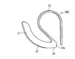
- FIG. 14 is a perspective view showing the configuration of the probe 20f according to the second embodiment of the present invention.
- symbol is attached
- the probe 20f shown in FIG. 14 has a substantially flat plate shape with a uniform thickness, and has a side surface curved in an arc shape at the tip, and the first contact that contacts the semiconductor integrated circuit 100 shown in FIG. 1 on this side surface. 1 and a second contact portion 28 that contacts the circuit board 30 shown in FIG. 1, and a connection portion that connects the first contact portion 21 and the second contact portion 28. 23 and an elastic portion 24 that extends from the second contact portion 28 and is partially curved in an arc shape and is elastically deformed by a load applied to the first contact portion 21 and the second contact portion 28.
- the second contact portion 28 has a side surface 28 a formed in a plane corresponding to the wall surface of the fixing member 13, and fixes the probe 20 f by contacting the wall surface of the fixing member 13.
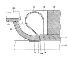
- 15 is a partial cross-sectional view showing a case where the probe 20f shown in FIG. 14 is introduced into the probe unit 1 shown in FIG.
- the probe 20 f held in the hole 14 of the fixing member 13 is in contact with the wall surface of the fixing member 13 at the side surface 28 a in the second contact portion 28.
- the side surface 28 a is formed along the wall surface of the fixing member 13, the protruding direction of the connection portion 23 and the first contact portion 21 from the slit 12 is adjusted by the contact of the second contact portion 28. It becomes possible.
- FIG. 16 is a partial cross-sectional view showing a state where the first contact portion 21 is pushed down by the semiconductor integrated circuit 100.
- the first contact portion 21 in contact with the electrode 101 and the second contact portion 28 in contact with the electrode 31 rotate on the surface of each electrode by the movement of the semiconductor integrated circuit 100 (in the direction of the arrow in the figure).
- the curved portion of the elastic portion 24 is elastically deformed by the load applied to the probe 20f.
- the broken line P 1 indicates the position of the probe 20f when no load is applied from the semiconductor integrated circuit 100 shown in FIG. 15.
- the side surface 28a contacting the wall surface of the fixing member 13 has a positioning effect. It can be easily arranged at a position.
- connect the fixing member 13 and the electrode 31, respectively has comprised R shape.
- the radius of the R shape is 0 ⁇ R ⁇ 0.1 (mm).
- the radius of the R shape is 0 ⁇ R ⁇ 50 ( ⁇ m).
- the second contact portion 28 has the R shape described above, the second contact portion can move the contact point along the electrode surface more efficiently, so that it is possible to further suppress wear of the electrode. .
- the side surface 28a may be formed on the probe 20 shown in FIG. 5 or the probes 20a to 20e shown in FIGS. A positioning effect can be obtained by bringing the second contact portion into contact with the wall surface of the fixing member 13.
- the semiconductor integrated circuit has been described as being a QFN having no external lead.
- the semiconductor integrated circuit 200 having a lead 201 (Quad Flat) Package: QFP).
- the contact probe according to the present invention is useful when electrical connection is made by connecting electrical circuit boards or the like.
- Probe unit 10 Probe holder 11 Accommodation part 12 Slit 13 Fixing member 14 Hole part 15 Opening part 20,20a, 20b, 20c, 20d, 20e, 20f Probe 21 1st contact part 22,28 2nd contact part 23,26 Connection Portion 24, 25, 27, 27a, 27b Elastic portion 30 Circuit board 31, 101 Electrode 100, 200 Semiconductor integrated circuit 201 Lead
Landscapes
- Physics & Mathematics (AREA)
- General Physics & Mathematics (AREA)
- Engineering & Computer Science (AREA)
- Computer Hardware Design (AREA)
- Microelectronics & Electronic Packaging (AREA)
- Measuring Leads Or Probes (AREA)
- Testing Of Individual Semiconductor Devices (AREA)
- Testing Or Measuring Of Semiconductors Or The Like (AREA)
Abstract
Description
図1は、本発明の実施の形態1にかかるプローブユニットの構成を示す斜視図である。図1に示すプローブユニット1は、検査対象物である半導体集積回路100の電気特性検査を行う際に使用する装置であって、半導体集積回路100と半導体集積回路100へ検査用信号を出力する回路基板30との間を電気的に接続する装置である。なお、本実施の形態1において、半導体集積回路100は、電極101を有するQFN(Quad Flat Non‐leaded Package)であるものとして説明する。
実施の形態1では、プローブの第2接触部が固定部材の壁面に当接しないものとして説明したが、本実施の形態2では、第2接触部が固定部材の壁面に当接している場合について説明する。図14は、本発明の実施の形態2にかかるプローブ20fの構成を示す斜視図である。なお、図1等で上述したプローブユニット1と同じ構成要素には同じ符号を付してある。
10 プローブホルダ
11 収容部
12 スリット
13 固定部材
14 穴部
15 開口部
20,20a,20b,20c,20d,20e,20f プローブ
21 第1接触部
22,28 第2接触部
23,26 接続部
24,25,27,27a,27b 弾性部
30 回路基板
31,101 電極
100,200 半導体集積回路
201 リード
Claims (10)
- 異なる基板間を接続する板厚が均一な略平板状のコンタクトプローブであって、
弧状に湾曲した側面を有し、この側面で一方の基板と接触する第1接触部と、
弧状に湾曲した側面を有し、この側面で他方の基板と接触する第2接触部と、
前記第1接触部および前記第2接触部を接続する接続部と、
前記第2接触部から延び、一部が弧状に湾曲された形状をなし、前記第1接触部および前記第2接触部に加わる荷重によって弾性変形する弾性部と、
を備えたことを特徴とするコンタクトプローブ。 - 前記弾性部の幅は、前記接続部の幅と比して小さいことを特徴とする請求項1に記載のコンタクトプローブ。
- 前記接続部は、弧状をなすことを特徴とする請求項1または2に記載のコンタクトプローブ。
- 前記弾性部は、一部が直線状をなすことを特徴とする請求項1~3のいずれか一つに記載のコンタクトプローブ。
- 前記弾性部は、前記第1接触部と接する第1の平面と、前記第1の平面と平行であって、前記第2接触部と接する第2の平面との間に位置することを特徴とする請求項1~3のいずれか一つに記載のコンタクトプローブ。
- 弧状に湾曲した側面を有し、この側面で一方の基板と接触する第1接触部と、弧状に湾曲した側面を有し、この側面で他方の基板と接触する第2接触部と、前記第1接触部および前記第2接触部を接続する接続部と、前記第2接触部から延び、一部が弧状に湾曲された形状をなし、前記第1接触部および前記第2接触部に加わる荷重によって弾性変形する弾性部と、を有する略平板状のコンタクトプローブと、
前記コンタクトプローブを保持する保持部と、
を備えたことを特徴とするプローブユニット。 - 前記保持部は、前記弾性部と等しい径を有し、前記弾性部の前記接続部側と異なる端部を収容して固定する穴部が設けられたことを特徴とする請求項6に記載のプローブユニット。
- 前記保持部は、前記第2接触部と少なくとも一箇所で接触することを特徴とする請求項6または7に記載のプローブユニット。
- 前記第2接触部は、荷重が加わらない状態で前記他方の基板および前記保持部とそれぞれ接触する接触箇所同士のうちで最短となる接触箇所同士を結ぶ外縁がR形状をなすことを特徴とする請求項8に記載のプローブユニット。
- 前記保持部は、前記コンタクトプローブを収容可能なスリットが形成されたことを特徴とする請求項6~9のいずれか一つに記載のプローブユニット。
Priority Applications (3)
| Application Number | Priority Date | Filing Date | Title |
|---|---|---|---|
| CN2011800127011A CN102782507A (zh) | 2010-03-15 | 2011-03-14 | 接触式探针及探针单元 |
| US13/634,025 US20130002281A1 (en) | 2010-03-15 | 2011-03-14 | Contact probe and probe unit |
| EP11756259.5A EP2560010A4 (en) | 2010-03-15 | 2011-03-14 | CONTACT PROBE AND PROBE UNIT |
Applications Claiming Priority (2)
| Application Number | Priority Date | Filing Date | Title |
|---|---|---|---|
| JP2010-057703 | 2010-03-15 | ||
| JP2010057703A JP2011191187A (ja) | 2010-03-15 | 2010-03-15 | コンタクトプローブおよびプローブユニット |
Publications (1)
| Publication Number | Publication Date |
|---|---|
| WO2011115074A1 true WO2011115074A1 (ja) | 2011-09-22 |
Family
ID=44649159
Family Applications (1)
| Application Number | Title | Priority Date | Filing Date |
|---|---|---|---|
| PCT/JP2011/055969 Ceased WO2011115074A1 (ja) | 2010-03-15 | 2011-03-14 | コンタクトプローブおよびプローブユニット |
Country Status (7)
| Country | Link |
|---|---|
| US (1) | US20130002281A1 (ja) |
| EP (1) | EP2560010A4 (ja) |
| JP (1) | JP2011191187A (ja) |
| KR (1) | KR20120112867A (ja) |
| CN (1) | CN102782507A (ja) |
| TW (1) | TW201200880A (ja) |
| WO (1) | WO2011115074A1 (ja) |
Families Citing this family (14)
| Publication number | Priority date | Publication date | Assignee | Title |
|---|---|---|---|---|
| TWI506281B (zh) * | 2013-07-15 | 2015-11-01 | Mpi Corp | Low impedance value of the probe module |
| CN105807213A (zh) * | 2016-05-30 | 2016-07-27 | 青岛港湾职业技术学院 | 一种用于扁平引脚芯片的测试装置 |
| KR101962644B1 (ko) * | 2017-08-23 | 2019-03-28 | 리노공업주식회사 | 검사프로브 및 이를 사용한 검사장치 |
| JP6908133B2 (ja) * | 2018-01-11 | 2021-07-21 | オムロン株式会社 | プローブピン、検査治具、検査ユニットおよび検査装置 |
| CN114441813A (zh) * | 2018-01-11 | 2022-05-06 | 欧姆龙株式会社 | 探针、检查工具、检查单元和检查装置 |
| WO2019138507A1 (ja) * | 2018-01-11 | 2019-07-18 | オムロン株式会社 | プローブピン、検査治具、検査ユニットおよび検査装置 |
| KR101974816B1 (ko) * | 2018-06-18 | 2019-05-03 | 박상량 | 판 스프링 타입의 연결핀 |
| JP7110817B2 (ja) * | 2018-08-09 | 2022-08-02 | オムロン株式会社 | 検査具、検査ユニットおよび検査装置 |
| JP2020134216A (ja) * | 2019-02-15 | 2020-08-31 | 株式会社サンケイエンジニアリング | 検査治具 |
| CN110994226B (zh) * | 2019-12-24 | 2021-12-10 | 海光信息技术股份有限公司 | 插槽、主板和处理装置 |
| WO2021207153A1 (en) * | 2020-04-07 | 2021-10-14 | Smiths Interconnect Americas, Inc. | Test socket for semiconductor integrated circuits |
| CN111579837B (zh) * | 2020-05-18 | 2022-09-20 | 武汉精毅通电子技术有限公司 | 一种适用于大电流高速信号测试的探针及连接器 |
| CN111579833B (zh) * | 2020-05-18 | 2022-12-23 | 武汉精毅通电子技术有限公司 | 一种适用于大电流高速信号测试的探针及连接器 |
| CN116699204A (zh) * | 2023-07-13 | 2023-09-05 | 渭南木王智能科技股份有限公司 | 弧形双头双动半导体测试探针 |
Citations (7)
| Publication number | Priority date | Publication date | Assignee | Title |
|---|---|---|---|---|
| JPH04277665A (ja) | 1991-03-06 | 1992-10-02 | Nec Corp | 半導体集積回路装置のソケット |
| JPH04118586U (ja) * | 1991-04-02 | 1992-10-23 | 日本航空電子工業株式会社 | 基板間接続用コネクタ |
| JPH0896905A (ja) * | 1994-09-26 | 1996-04-12 | Japan Aviation Electron Ind Ltd | 平行基板用コネクタ |
| JPH11344508A (ja) * | 1998-06-02 | 1999-12-14 | Japan Electronic Materials Corp | プローブ及びこのプローブを用いたプローブカード |
| JP2002298949A (ja) * | 2001-03-29 | 2002-10-11 | Japan Aviation Electronics Industry Ltd | コネクタ |
| JP2003123924A (ja) * | 2001-10-05 | 2003-04-25 | Molex Inc | 半導体パッケージのソケット、及びコンタクト |
| JP2007503103A (ja) * | 2003-06-11 | 2007-02-15 | シンチ コネクターズ インコーポレーテッド | 電気コネクタ |
Family Cites Families (12)
| Publication number | Priority date | Publication date | Assignee | Title |
|---|---|---|---|---|
| US3877064A (en) * | 1974-02-22 | 1975-04-08 | Amp Inc | Device for connecting leadless integrated circuit packages to a printed-circuit board |
| US3993384A (en) * | 1975-05-12 | 1976-11-23 | E. I. Du Pont De Nemours And Company | Connector block |
| US4052118A (en) * | 1975-05-30 | 1977-10-04 | Amp Incorporated | Contact carrying spring member |
| GB2008333B (en) * | 1977-11-14 | 1982-05-26 | Amp Inc | Electrical connector |
| US4268102A (en) * | 1979-10-04 | 1981-05-19 | Amp Incorporated | Low impedance electrical connecting means for spaced-apart conductors |
| US4494807A (en) * | 1982-12-27 | 1985-01-22 | Amp Incorporated | Low profile chip carrier contact |
| US4684184A (en) * | 1986-01-14 | 1987-08-04 | Amp Incorporated | Chip carrier and carrier socket for closely spaced contacts |
| FR2703839B1 (fr) * | 1993-04-09 | 1995-07-07 | Framatome Connectors France | Connecteur intermédiaire entre carte de circuit imprimé et substrat à circuits électroniques. |
| JPH1022423A (ja) * | 1996-07-08 | 1998-01-23 | Advantest Corp | Sojパッケージ用icソケット |
| JP3406180B2 (ja) * | 1997-04-21 | 2003-05-12 | ヒロセ電機株式会社 | 中間電気コネクタ |
| JP4279039B2 (ja) * | 2003-04-22 | 2009-06-17 | 株式会社エンプラス | 電気部品用ソケット |
| US7094062B2 (en) * | 2003-07-24 | 2006-08-22 | Molex Incorporated | Land grid array connector |
-
2010
- 2010-03-15 JP JP2010057703A patent/JP2011191187A/ja active Pending
-
2011
- 2011-03-14 US US13/634,025 patent/US20130002281A1/en not_active Abandoned
- 2011-03-14 CN CN2011800127011A patent/CN102782507A/zh active Pending
- 2011-03-14 WO PCT/JP2011/055969 patent/WO2011115074A1/ja not_active Ceased
- 2011-03-14 EP EP11756259.5A patent/EP2560010A4/en not_active Withdrawn
- 2011-03-14 KR KR1020127023232A patent/KR20120112867A/ko not_active Ceased
- 2011-03-14 TW TW100108490A patent/TW201200880A/zh unknown
Patent Citations (7)
| Publication number | Priority date | Publication date | Assignee | Title |
|---|---|---|---|---|
| JPH04277665A (ja) | 1991-03-06 | 1992-10-02 | Nec Corp | 半導体集積回路装置のソケット |
| JPH04118586U (ja) * | 1991-04-02 | 1992-10-23 | 日本航空電子工業株式会社 | 基板間接続用コネクタ |
| JPH0896905A (ja) * | 1994-09-26 | 1996-04-12 | Japan Aviation Electron Ind Ltd | 平行基板用コネクタ |
| JPH11344508A (ja) * | 1998-06-02 | 1999-12-14 | Japan Electronic Materials Corp | プローブ及びこのプローブを用いたプローブカード |
| JP2002298949A (ja) * | 2001-03-29 | 2002-10-11 | Japan Aviation Electronics Industry Ltd | コネクタ |
| JP2003123924A (ja) * | 2001-10-05 | 2003-04-25 | Molex Inc | 半導体パッケージのソケット、及びコンタクト |
| JP2007503103A (ja) * | 2003-06-11 | 2007-02-15 | シンチ コネクターズ インコーポレーテッド | 電気コネクタ |
Non-Patent Citations (1)
| Title |
|---|
| See also references of EP2560010A4 |
Also Published As
| Publication number | Publication date |
|---|---|
| EP2560010A1 (en) | 2013-02-20 |
| CN102782507A (zh) | 2012-11-14 |
| EP2560010A4 (en) | 2013-07-31 |
| US20130002281A1 (en) | 2013-01-03 |
| TW201200880A (en) | 2012-01-01 |
| JP2011191187A (ja) | 2011-09-29 |
| KR20120112867A (ko) | 2012-10-11 |
Similar Documents
| Publication | Publication Date | Title |
|---|---|---|
| WO2011115074A1 (ja) | コンタクトプローブおよびプローブユニット | |
| JP6110086B2 (ja) | 接触検査装置 | |
| CN102183680B (zh) | 连接装置 | |
| JP6255914B2 (ja) | 検査治具 | |
| KR101662937B1 (ko) | 공간변형기능을 가진 검사접촉장치 | |
| WO2007094237A1 (ja) | 導電性接触子および導電性接触子ユニット | |
| KR20160084014A (ko) | 검사접촉장치 | |
| KR20190011765A (ko) | 전기적 접속장치 및 접촉자 | |
| JP2011232313A (ja) | コンタクトプローブおよびプローブユニット | |
| CN112345802A (zh) | 电触头及电连接装置 | |
| JPWO2010117058A1 (ja) | コンタクトプローブおよびプローブユニット | |
| WO2012008541A1 (ja) | コンタクトプローブおよびプローブユニット | |
| JP2011133354A (ja) | コンタクトプローブおよびプローブユニット | |
| JP2011203087A (ja) | コンタクトプローブ | |
| JP2013061189A (ja) | コンタクトプローブおよびプローブユニット | |
| JP2013061188A (ja) | コンタクトプローブおよびプローブユニット | |
| JP6170176B2 (ja) | ソケット取付構造およびばね部材 | |
| JP2013148433A (ja) | コンタクトプローブおよびプローブユニット | |
| WO2012063858A1 (ja) | プローブユニット | |
| WO2012118026A1 (ja) | コンタクトプローブおよびプローブユニット | |
| KR101680319B1 (ko) | 액정 패널 테스트용 프로브 블록 | |
| WO2002103373A1 (en) | Conductive contactor and electric probe unit | |
| JP2007127488A (ja) | プローブカード | |
| CN100486046C (zh) | Ic插座 | |
| JP4886422B2 (ja) | 四端子測定用プローブ |
Legal Events
| Date | Code | Title | Description |
|---|---|---|---|
| WWE | Wipo information: entry into national phase |
Ref document number: 201180012701.1 Country of ref document: CN |
|
| 121 | Ep: the epo has been informed by wipo that ep was designated in this application |
Ref document number: 11756259 Country of ref document: EP Kind code of ref document: A1 |
|
| ENP | Entry into the national phase |
Ref document number: 20127023232 Country of ref document: KR Kind code of ref document: A |
|
| WWE | Wipo information: entry into national phase |
Ref document number: 13634025 Country of ref document: US |
|
| WWE | Wipo information: entry into national phase |
Ref document number: 2011756259 Country of ref document: EP |
|
| NENP | Non-entry into the national phase |
Ref country code: DE |