WO2011125363A1 - Élément à électroluminescence organique, dispositif d'affichage à électroluminescence organique et appareil d'affichage à électroluminescence organique - Google Patents
Élément à électroluminescence organique, dispositif d'affichage à électroluminescence organique et appareil d'affichage à électroluminescence organique Download PDFInfo
- Publication number
- WO2011125363A1 WO2011125363A1 PCT/JP2011/051650 JP2011051650W WO2011125363A1 WO 2011125363 A1 WO2011125363 A1 WO 2011125363A1 JP 2011051650 W JP2011051650 W JP 2011051650W WO 2011125363 A1 WO2011125363 A1 WO 2011125363A1
- Authority
- WO
- WIPO (PCT)
- Prior art keywords
- organic
- layer
- light
- phosphor layer
- distribution characteristic
- Prior art date
- Legal status (The legal status is an assumption and is not a legal conclusion. Google has not performed a legal analysis and makes no representation as to the accuracy of the status listed.)
- Ceased
Links
Images




Classifications
-
- H—ELECTRICITY
- H05—ELECTRIC TECHNIQUES NOT OTHERWISE PROVIDED FOR
- H05B—ELECTRIC HEATING; ELECTRIC LIGHT SOURCES NOT OTHERWISE PROVIDED FOR; CIRCUIT ARRANGEMENTS FOR ELECTRIC LIGHT SOURCES, IN GENERAL
- H05B33/00—Electroluminescent light sources
- H05B33/02—Details
-
- H—ELECTRICITY
- H05—ELECTRIC TECHNIQUES NOT OTHERWISE PROVIDED FOR
- H05B—ELECTRIC HEATING; ELECTRIC LIGHT SOURCES NOT OTHERWISE PROVIDED FOR; CIRCUIT ARRANGEMENTS FOR ELECTRIC LIGHT SOURCES, IN GENERAL
- H05B33/00—Electroluminescent light sources
- H05B33/12—Light sources with substantially two-dimensional [2D] radiating surfaces
- H05B33/22—Light sources with substantially two-dimensional [2D] radiating surfaces characterised by the chemical or physical composition or the arrangement of auxiliary dielectric or reflective layers
- H05B33/24—Light sources with substantially two-dimensional [2D] radiating surfaces characterised by the chemical or physical composition or the arrangement of auxiliary dielectric or reflective layers of metallic reflective layers
-
- H—ELECTRICITY
- H05—ELECTRIC TECHNIQUES NOT OTHERWISE PROVIDED FOR
- H05B—ELECTRIC HEATING; ELECTRIC LIGHT SOURCES NOT OTHERWISE PROVIDED FOR; CIRCUIT ARRANGEMENTS FOR ELECTRIC LIGHT SOURCES, IN GENERAL
- H05B33/00—Electroluminescent light sources
- H05B33/12—Light sources with substantially two-dimensional [2D] radiating surfaces
- H05B33/26—Light sources with substantially two-dimensional [2D] radiating surfaces characterised by the composition or arrangement of the conductive material used as an electrode
-
- H—ELECTRICITY
- H05—ELECTRIC TECHNIQUES NOT OTHERWISE PROVIDED FOR
- H05B—ELECTRIC HEATING; ELECTRIC LIGHT SOURCES NOT OTHERWISE PROVIDED FOR; CIRCUIT ARRANGEMENTS FOR ELECTRIC LIGHT SOURCES, IN GENERAL
- H05B33/00—Electroluminescent light sources
- H05B33/12—Light sources with substantially two-dimensional [2D] radiating surfaces
- H05B33/26—Light sources with substantially two-dimensional [2D] radiating surfaces characterised by the composition or arrangement of the conductive material used as an electrode
- H05B33/28—Light sources with substantially two-dimensional [2D] radiating surfaces characterised by the composition or arrangement of the conductive material used as an electrode of translucent electrodes
-
- H—ELECTRICITY
- H10—SEMICONDUCTOR DEVICES; ELECTRIC SOLID-STATE DEVICES NOT OTHERWISE PROVIDED FOR
- H10K—ORGANIC ELECTRIC SOLID-STATE DEVICES
- H10K50/00—Organic light-emitting devices
-
- H—ELECTRICITY
- H10—SEMICONDUCTOR DEVICES; ELECTRIC SOLID-STATE DEVICES NOT OTHERWISE PROVIDED FOR
- H10K—ORGANIC ELECTRIC SOLID-STATE DEVICES
- H10K50/00—Organic light-emitting devices
- H10K50/80—Constructional details
- H10K50/85—Arrangements for extracting light from the devices
- H10K50/852—Arrangements for extracting light from the devices comprising a resonant cavity structure, e.g. Bragg reflector pair
-
- H—ELECTRICITY
- H10—SEMICONDUCTOR DEVICES; ELECTRIC SOLID-STATE DEVICES NOT OTHERWISE PROVIDED FOR
- H10K—ORGANIC ELECTRIC SOLID-STATE DEVICES
- H10K59/00—Integrated devices, or assemblies of multiple devices, comprising at least one organic light-emitting element covered by group H10K50/00
- H10K59/30—Devices specially adapted for multicolour light emission
- H10K59/38—Devices specially adapted for multicolour light emission comprising colour filters or colour changing media [CCM]
-
- H—ELECTRICITY
- H10—SEMICONDUCTOR DEVICES; ELECTRIC SOLID-STATE DEVICES NOT OTHERWISE PROVIDED FOR
- H10K—ORGANIC ELECTRIC SOLID-STATE DEVICES
- H10K59/00—Integrated devices, or assemblies of multiple devices, comprising at least one organic light-emitting element covered by group H10K50/00
- H10K59/80—Constructional details
- H10K59/875—Arrangements for extracting light from the devices
- H10K59/876—Arrangements for extracting light from the devices comprising a resonant cavity structure, e.g. Bragg reflector pair
Definitions
- the present invention relates to an organic EL element, an organic EL display, and an organic EL display device.
- a technique for displaying a moving image by simple matrix driving or a technique for displaying a moving image by active matrix driving of an organic EL element using a thin film transistor (TFT) is known.
- Patent Document 1 discloses a full color by combining an organic EL element having a light emitting layer that emits blue light or blue green light and a fluorescent material part that absorbs light emitted from the light emitting layer and emits visible light. The method of displaying is described.
- Patent Documents 2, 3, 4, and 5 describe organic EL elements having an optical microresonator (microcavity) structure.
- a color conversion unit that absorbs light emitted from the organic EL element and emits visible light fluorescence is used for all of the red pixel (R), green pixel (G), and blue pixel (B).
- R red pixel
- G green pixel
- B blue pixel
- Patent Document 2 discloses that light in the blue region is emitted from the organic EL element, the light in the blue region emitted from the green pixel is converted into light in the green region, and the light in the blue region emitted from the red pixel is converted into light.
- Patent Document 5 describes a configuration in which a light emitting layer and a color exchange layer are arranged between a pair of light reflecting layers.
- the above-described conventional method of separately coating the organic light emitting layer requires a mask having a size equal to or larger than the size of the substrate. Therefore, with the recent increase in size of the substrate, fabrication and processing of a mask corresponding to the large substrate is required. Need to do.
- the size of the substrate is increasing, such as G6, G8, and G10.
- a very thin metal generally film thickness: 50 to 100 nm
- this method requires high mask processing accuracy and alignment accuracy.
- the mask processing accuracy and alignment accuracy are low, color mixing due to mixing of the light emitting layers may occur.
- the width of the insulating layer provided between the pixels is increased, the area of the non-light emitting portion is reduced when the area of the pixel is determined in advance. That is, it leads to a decrease in the aperture ratio of the pixel, leading to a decrease in luminance, an increase in power consumption, and a decrease in life.
- the deposition source is disposed below the substrate, and the organic layer is deposited by depositing the organic material from the bottom to the top.
- the substrate becomes larger (the mask becomes larger)
- the mask bends at the center.
- a similar problem occurs due to thermal expansion of the mask during vapor deposition.
- the mask bends, it also causes the color mixture described above.
- the mask is severely bent, a portion in which the organic layer is not formed or the upper and lower electrodes leak is connected.
- the mask becomes unusable due to deterioration after being used a specific number of times. Therefore, the problem of increasing the size of the mask leads to an increase in cost in manufacturing the display. In particular, in an organic EL display, preventing cost increase is a very important issue.
- the peak wavelength in the emission spectrum of light from the light emitting layer cannot be made sufficiently short, and the half width is also increased. Is as wide as about 80 nm, and light having sufficient color purity cannot be obtained.
- an organic phosphorescent material having luminous efficiency superior to that of the organic phosphor material is used for the light emitting layer, the color purity is further lowered. For this reason, in an organic EL element, it is important to improve the light emission intensity and color purity.
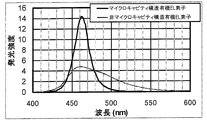
- FIG. 10 shows an emission spectrum from an organic EL element having a microcavity structure and an emission spectrum from an organic EL element having a non-microcavity structure.
- the organic EL element has a microcavity structure, the emission intensity and color purity from the organic EL element are improved compared to the non-microcavity structure, so that the luminous efficiency is increased. Can do.
- Patent Documents 2, 3, 4, and 5 using the microcavity structure have the following problems.
- the blue region light emitted from the organic EL element is fluorescently converted by a phosphor layer or the like to emit light.
- the light in the blue region emitted from the organic EL element is directly used.
- the light from the organic EL element having a microcavity structure has directivity. Since the light from the red pixel and the green pixel is converted into isotropic light by the phosphor layer, luminance and color purity do not change depending on the viewing angle. On the other hand, since light from a blue pixel that directly uses light from an organic EL element becomes directional light, luminance and color purity change depending on the viewing angle. That is, there arises a problem that the luminance and color purity of light from the red and green pixels and the luminance and color purity of light from the blue pixel are shifted depending on the viewing angle.
- Patent Document 5 is a method for obtaining a microcavity effect in a layer including a light emitting layer and a color conversion layer.
- light from pixels of all colors is directional. Since it becomes a certain light, the problem that a viewing angle characteristic worsens newly arises.
- the present invention has been made in view of the above-described problems of the prior art, and an object thereof is an organic EL display and an organic EL display device including an organic EL element having a structure that exhibits a microcavity effect.
- An object of the present invention is to provide an organic EL device having good viewing angle characteristics and having a small deviation in luminance and color purity of pixels of each color depending on the viewing angle at low cost.
- an organic EL device includes a reflective electrode, a semitransparent electrode, an organic EL layer that is sandwiched between the reflective electrode and the semitransparent electrode, and emits blue light.
- a red phosphor layer for converting light from the organic EL layer into light in the red region a green phosphor layer for converting light from the organic EL layer into light in the green region, and light from the organic EL layer.
- a blue pixel composed of a light distribution characteristic adjusting layer for adjusting a light distribution characteristic, wherein the reflective electrode and the semi-transparent electrode have a structure exhibiting a microcavity effect.
- the structure that exhibits the microcavity effect emits light having directivity and high luminance in the front direction (hereinafter also referred to as “front luminance”), and thus high luminous efficiency is obtained.
- front luminance light having directivity and high luminance in the front direction
- the red phosphor layer and the green phosphor layer can absorb light having directivity from the organic EL layer and emit more isotropic light.
- the blue pixel adjusts the light distribution characteristics so that it becomes isotropic light in order to adjust the light distribution characteristics (for example, luminance, color purity, etc.) of the light from the organic EL layer by the light distribution characteristic adjustment layer. It is also possible to do.
- the organic EL element according to the present invention when used for a display and a display device, a high-quality organic EL display and an organic EL display device can be provided. Moreover, this invention can be utilized suitably also for a large sized display and a display apparatus.
- the organic EL display according to the present invention includes any one of the organic EL elements described above.
- the organic EL display device includes any one of the above-described organic EL displays.
- the organic EL element according to the present invention includes a reflective electrode, a semitransparent electrode, an organic EL layer that is sandwiched between the reflective electrode and the semitransparent electrode, and emits blue light, and the organic EL layer.
- the red phosphor layer that converts light from the red region into light, the green phosphor layer that converts light from the organic EL layer into light in the green region, and the light distribution characteristics of the light from the organic EL layer A blue pixel composed of a light distribution characteristic adjusting layer to be adjusted, and since the reflective electrode and the translucent electrode are structured to exhibit a microcavity effect, have a good viewing angle characteristic,
- an organic EL element in which a deviation in luminance and color purity of each color pixel depending on the viewing angle can be provided at low cost.
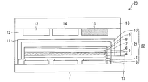
- FIG. 1 is a cross-sectional view schematically showing a schematic configuration of a main part of an organic EL display according to an embodiment of the present invention.
- FIG. 1 shows a portion of an organic EL element included in the organic EL display 20.
- the organic EL display 20 includes, as organic EL elements, a substrate 1, an organic EL unit 22, an inorganic sealing film 11, a resin sealing film 12, a red phosphor layer 13, and a green phosphor layer 14.
- An optical property adjusting layer 15, a sealing substrate 16, and a partition wall layer 17 are provided.
- the reflective electrode 2, the edge cover 3, the partition wall layer 17, the organic EL layer 21, and the translucent electrode 10 in the organic EL portion 22 are laminated in this order.
- an active element such as a TFT for driving the pixel, the organic EL display 20 or the like may be formed on the substrate 1.
- the partition wall layer 17 is an insulating layer formed outside the organic EL portion 22.
- the partition layer 17 can hold a coating liquid to be applied.
- the organic EL part 22 is composed of the reflective electrode 2, the semitransparent electrode 10, the organic EL layer 21, and the edge cover 3.
- the reflective electrode 2 and the translucent electrode 10 are a pair of electrodes that function as a pair, and sandwich the organic EL layer 21.
- the reflective electrode 2 is an anode and is an electrode that injects holes into the organic EL layer 21.
- the translucent electrode 10 is a cathode and an electrode that injects electrons into the organic EL layer 21.
- the organic EL layer 21 is a layer that emits blue light and is sandwiched between the reflective electrode 2 and the translucent electrode 10, and includes a light emitting layer 6 containing an organic light emitting material and a layer for injecting or transporting charges ( Hereinafter, a hole injection layer 4, a hole transport layer 5, a hole prevention layer 7, an electron transport layer 8, and an electron injection layer 9 functioning as a “charge injection transport layer”) are provided.
- the light emitted from the organic EL layer 21 passes through the translucent electrode 10 and is extracted outside.
- the edge cover 3 is an insulating cover formed between the reflective electrode 2 and the translucent electrode 10.
- the edge cover 3 can prevent leakage between the reflective electrode 2 and the translucent electrode 10 at the edge portion that becomes the end of the reflective electrode 2.
- the organic EL unit 22 uses the principle of a microcavity that utilizes multiple interference between the reflective electrode 2 and the translucent electrode 10, and has a structure that exhibits a so-called microcavity effect (optical microresonator structure). have. For example, it is more desirable to form the microcavity effect by setting the thickness between the reflective electrode 2 and the semitransparent electrode 10 so as to match the wavelength of light to be enhanced.
- the organic EL layer 21 is sandwiched between the pair of reflective electrodes 2 and the translucent electrode 10.
- the reflective electrode 2 is made of a mirror-surface totally reflective material
- the semi-transparent electrode 10 is made of a semi-transmissive material of a dielectric mirror
- the thickness of the organic EL layer 21 is formed so as to match the wavelength of light to be enhanced.
- the light component having a shifted wavelength is amplified to a desired wavelength by repeating multiple reflections between the reflective electrode 2 and the translucent electrode 10 and resonating. Output.
- the organic EL element having an optical microresonator structure can enhance light emission at a desired wavelength (see FIG. 10).
- the organic EL unit 22 in the present embodiment can enhance the intensity of light in the blue region.
- the distance between the reflective electrode 2 and the translucent electrode 10 can be adjusted by adjusting the film thickness of the organic EL layer 21.
- the inorganic sealing film 11 is a sealing film made of an inorganic compound
- the resin sealing film 12 is a sealing film made of a resin.
- the red phosphor layer 13 is a phosphor layer composed of a red phosphor that absorbs blue region light from the organic EL unit 22 and converts it into red region light, and functions as a red pixel.
- the green phosphor layer 14 is a phosphor layer composed of a green phosphor that absorbs blue region light from the organic EL unit 22 and converts it into green region light, and functions as a green pixel. Thereby, in the red pixel and the green pixel, the red phosphor layer 13 and the green phosphor layer 14 absorb light having directivity from the organic EL unit 22 having the optical microresonator structure, and isotropic. Light can be emitted.
- the light distribution characteristic adjustment layer 15 is a layer that adjusts the light distribution characteristic of the light from the organic EL unit 22, and functions as a blue pixel.
- the “light distribution characteristics” refer to characteristics relating to light brightness, color purity, and the like depending on viewing angles.
- the sealing substrate 16 is a substrate for sealing the above-described constituent members.
- Substrate 1 As the substrate 1, for example, an inorganic material substrate made of glass, quartz or the like, a plastic substrate made of polyethylene terephthalate, polycarbazole, polyimide or the like, an insulating substrate such as a ceramic substrate made of alumina or the like, aluminum (Al), iron (Fe ) And the like. Further, the surface of these substrates is coated with an insulator made of silicon oxide (SiO 2 ), an organic insulating material or the like, or the surface of a metal substrate made of Al or the like is insulated by a method such as anodic oxidation. It may be a coated substrate or the like.
- a plastic substrate or a metal substrate because a curved portion, a bent portion, and the like can be formed without stress.
- a substrate in which a plastic substrate is coated with an inorganic material or a substrate in which a metal substrate is coated with an inorganic insulating material is more preferable.
- leakage may occur due to the protrusion of the metal substrate, but such a problem can be prevented by the above-described configuration.
- the film thickness of the organic EL layer is often very thin, about 100 to 200 nm, and it is known that leakage (short-circuiting) occurs in the current in the pixel portion due to the protrusions of the substrate.
- a TFT may be formed on the substrate 1 as an active element.
- the substrate 1 it is preferable to use as the substrate 1 a substrate that does not melt at a temperature of 500 ° C. or less and does not cause distortion.
- a metal substrate it is preferable to use a metal substrate that is an iron-nickel alloy having a linear expansion coefficient of 1 ⁇ 10 ⁇ 5 / ° C. or less.
- substrate 1 is comparable as glass, TFT can be formed on the board
- a plastic substrate since the plastic substrate has a relatively low heat-resistant temperature, first, a TFT is formed on another glass substrate, and then this TFT is transferred onto the substrate 1, whereby the TFT Can be transferred and formed.
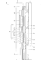
- FIG. 2 is a diagram showing a partial configuration of a circuit used by the organic EL display device according to the embodiment of the present invention.
- the circuit 30 includes a gate line 31, a signal line 32, a power supply line 33, a switching TFT 34, a driving TFT (active element) 35, a storage capacitor 36, an organic EL unit 22, and a ground line 38.
- the circuit 30 includes a plurality of gate lines 31 and a plurality of signal lines 32, and two TFTs, a switching TFT 34 and a driving TFT 35, are arranged for each pixel.
- the switching TFT 34 is disposed at the intersection between the gate line 31 and the signal line 32.
- the driving TFT 35 is electrically connected to the reflective electrode 2 in the organic EL unit 22. Note that the organic EL display 20 can be driven by a voltage-driven digital gradation method or the like.
- the circuit 30 may be electrically connected to an external drive circuit (scanning line electrode circuit (source driver), data signal electrode circuit (gate driver), power supply circuit) in order to drive each organic EL unit 22. Good.
- an external drive circuit scanning line electrode circuit (source driver), data signal electrode circuit (gate driver), power supply circuit
- the wavelength corresponding to the maximum value of the emission intensity of the light emitted from the organic EL unit 22 is preferably 400 nm or more and 480 nm or less.
- the maximum value of the light emission intensity of the light emitted from the organic EL portion 22 is reduced. If the wavelength corresponding to is 400 nm or more, the luminous efficiency and lifetime can be improved. In addition, the amount of absorption of the phosphor decreases with respect to light of 480 nm or more.
- the green phosphor generally has an abrupt decrease in absorption with respect to light having a long wavelength of 480 nm or longer. Therefore, if the wavelength is 480 nm or less, the phosphor, in particular, the green phosphor can be efficiently excited by the light from the organic EL unit 22 to emit light.
- the manufacturing cost and the material cost are significantly higher than those of the conventional separate coloring method in which the organic EL element is patterned into red, green, and blue pixels. It is possible to reduce it.
- this embodiment since the organic EL unit 22 having an optical microresonator structure is used, good light emission efficiency can be obtained and the lifetime can be extended, so that the cost and power consumption can be reduced. be able to. Furthermore, this embodiment can be suitably used as a large display and a display device.
- Organic EL layer 21 in this embodiment has a multilayer structure of the light emitting layer 6 and the charge injecting and transporting layer.
- the organic EL layer 21 is not limited to the configuration of the present embodiment, and may have the following configurations (1) to (9), for example.
- Each of the light emitting layer 6, the hole injection layer 4, the hole transport layer 5, the hole prevention layer 7, the electron prevention layer, the electron transport layer 8 and the electron injection layer 9 may have a single layer structure or a multilayer. It may be a structure.
- the film thickness of each layer in the organic EL layer 21 may be about 1 nm to 1000 nm, but is preferably 10 nm to 200 nm. If the film thickness is 10 nm or more, good physical properties (charge injection characteristics, transport characteristics, confinement characteristics, etc.) can be obtained for each layer of the organic EL layer 21. In addition, pixel defects due to foreign matters such as dust can be prevented. Moreover, if the film thickness is 200 nm or less, it is possible to prevent the drive voltage from increasing due to the resistance component of the organic EL layer 21 and to reduce power consumption.
- the light emitting layer 6 preferably contains a light emitting material (organic light emitting material) made of an organic compound.
- the light emitting layer 6 may be composed of, for example, only an organic light emitting material, or may be composed of a combination of a light emitting dopant and a host material.
- a hole transport material, an electron transport material, an additive (a donor, an acceptor, etc.) etc. may be contained arbitrarily.
- distributed in a polymeric material (binding resin) or an inorganic material may be sufficient. Especially, it is preferable to use what disperse
- the organic light emitting material a known light emitting material used for an organic EL layer or the like can be suitably used.
- a low molecular light emitting material, a polymer light emitting material, or the like can be used.
- a fluorescent material, a phosphorescent material, or the like can be used as the light-emitting material.
- Examples of the low-molecular light emitting material include fluorescent organic materials such as aromatic dimethylidene compounds, oxadiazole compounds, triazole derivatives, styrylbenzene compounds, and fluorenone derivatives.
- Examples of the aromatic dimethylidene compound include 4,4'-bis (2,2'-diphenylvinyl) -biphenyl (DPVBi).
- Examples of the oxadiazole compound include 5-methyl-2- [2- [4- (5-methyl-2-benzoxazolyl) phenyl] vinyl] benzoxazole.
- Examples of the triazole derivative include 3- (4-biphenylyl) -4-phenyl-5-t-butylphenyl-1,2,4-triazole (TAZ).
- Examples of the styrylbenzene compound include 1,4-bis (2-methylstyryl) benzene.
- polymer light emitting material examples include polyphenylene vinylene derivatives and polyspiro derivatives.
- polyphenylene vinylene derivative examples include poly (2-decyloxy-1,4-phenylene) (DO-PPP).
- polyspiro derivative examples include poly (9,9-dioctylfluorene) (PDAF).
- a known dopant material used for an organic EL layer or the like can be suitably used.
- dopant materials include fluorescent materials, phosphorescent organic metal complexes, and the like.
- fluorescent material include styryl derivatives.
- phosphorescent organometallic complexes include bis [(4,6-difluorophenyl) -pyridinato-N, C2 ′] picolinate iridium (III) (FIrpic), bis (4 ′, 6′-difluorophenylpolydinato) tetrakis ( 1-pyrazoyl) borate, iridium (III) (FIr6) and the like.
- a host material when using a dopant a known host material used for an organic EL layer or the like can be suitably used.
- host materials include the above-described low-molecular light-emitting materials, the above-described polymer light-emitting materials, carbazole derivatives, aniline derivatives, and fluorene derivatives.
- carbazole derivative include 4,4′-bis (carbazole) biphenyl, 9,9-di (4-dicarbazole-benzyl) fluorene (CPF), 3,6-bis (triphenylsilyl) carbazole (mCP), ( PCF).
- aniline derivatives include 4- (diphenylphosphoyl) -N, N-diphenylaniline (HM-A1).
- Fluorene derivatives include 1,3-bis (9-phenyl-9H-fluoren-9-yl) benzene (mDPFB), 1,4-bis (9-phenyl-9H-fluoren-9-yl) benzene (pDPFB) Etc.
- the charge injection transport layer is divided into a charge injection layer (hole injection layer 4 and electron injection layer 9) and a charge transport layer (hole transport layer 5 and electron transport layer 8).
- a charge injection layer hole injection layer 4 and electron injection layer 9
- a charge transport layer hole transport layer 5 and electron transport layer 8
- the charge injecting and transporting layer may be composed of only the materials exemplified below, but may optionally contain additives (donor, acceptor, etc.), etc., and these materials are polymeric materials (
- the resin may be dispersed in a binding resin) or an inorganic material.
- the material used for the charge injecting and transporting layer known materials used for the charge injecting and transporting layer such as an organic EL layer and an organic photoconductor can be used.
- the material includes a material for injecting or transporting holes (hereinafter also referred to as “hole injection / transport material”) and a material for injecting or transporting electrons (hereinafter also referred to as “electron injection / transport material”). Divided. Although these specific compounds are illustrated below, this invention is not limited to these materials.
- Examples of the hole injecting and transporting material include an oxide, an inorganic p-type semiconductor material, a porphyrin compound, an aromatic tertiary amine compound, a low molecular material, and a polymer material.
- Examples of the oxide include vanadium oxide (V 2 O 5 ) and molybdenum oxide (MoO 2 ).
- Aromatic tertiary amine compounds include N, N′-bis (3-methylphenyl) -N, N′-bis (phenyl) -benzidine (TPD), N, N′-di (naphthalen-1-yl) ) -N, N′-diphenyl-benzidine (NPD) and the like.
- low molecular weight material examples include hydrazone compounds, quinacridone compounds, styrylamine compounds, and the like.
- Polymer materials include polyaniline (PANI), polyaniline-camphor sulfonic acid (PANI-CSA), 3,4-polyethylenedioxythiophene / polystyrene sulfonate (PEDOT / PSS), poly (triphenylamine) derivative (Poly) -TPD), polyvinylcarbazole (PVCz), poly (p-phenylene vinylene) (PPV), poly (p-naphthalene vinylene) (PNV) and the like.
- the hole injection layer 4 it is preferable to use a material having a lower energy level of the highest occupied molecular orbital (HOMO) than the hole injection / transport material used for the hole transport layer 5.
- the hole transport layer 5 it is preferable to use a material having a higher hole mobility than the hole injection transport material used for the hole injection layer 4.
- the above-described hole injecting and transporting material doped with an acceptor.
- an acceptor the well-known acceptor material used for organic EL can be used. Although these specific compounds are illustrated below, this invention is not limited to these materials.
- the acceptor material examples include an inorganic material, a compound having a cyano group, a compound having a nitro group, and an organic material.
- Inorganic materials include gold (Au), platinum (Pt), tungsten (W), iridium (Ir), phosphoryl chloride (POCl 3 ), arsenic hexafluoride (AsF 6 ), chlorine (Cl), bromine (Br) , Iodine (I), vanadium oxide (V 2 O 5 ), molybdenum oxide (MoO 2 ), and the like.
- Examples of the compound having a cyano group include TCNQ (7,7,8,8, -tetracyanoquinodimethane), TCNQF 4 (tetrafluorotetracyanoquinodimethane), TCNE (tetracyanoethylene), HCNB (hexacyanobutadiene). And DDQ (dicyclodicyanobenzoquinone).
- Examples of the compound having a nitro group include TNF (trinitrofluorenone) and DNF (dinitrofluorenone).
- Examples of the organic material include fluoranyl, chloranil, bromanyl and the like. Among these, compounds having a cyano group such as TCNQ, TCNQF 4 , TCNE, HCNB, DDQ and the like are preferable because the carrier concentration can be increased more effectively.
- Examples of the electron injecting and transporting material include inorganic materials that are n-type semiconductors, oxadiazole derivatives, triazole derivatives, thiopyrazine dioxide derivatives, benzoquinone derivatives, naphthoquinone derivatives, anthraquinone derivatives, diphenoquinone derivatives, fluorenone derivatives, benzodifuran derivatives, etc. Low molecular materials; polymer materials such as poly (oxadiazole) (Poly-OXZ) and polystyrene derivatives (PSS) can be mentioned.
- examples of the electron injection material include fluorides such as lithium fluoride (LiF) and barium fluoride (BaF 2 ), and oxides such as lithium oxide (Li 2 O).
- the electron injection layer 9 it is preferable to use a material having a higher energy level of the lowest unoccupied molecular orbital (LUMO) than the electron injection transport material used for the electron transport layer 8.
- the electron transport layer 8 is preferably a material having a higher electron mobility than the electron injection transport material used for the electron injection layer 9.
- the electron injection / transport material In order to further improve the electron injection / transport property, it is preferable to dope the electron injection / transport material with a donor.
- a donor the well-known donor material used for organic EL can be used. Although these specific compounds are illustrated below, this invention is not limited to these materials.
- donor materials include inorganic materials, compounds having an aromatic tertiary amine as a skeleton, condensed polycyclic compounds, and organic materials.
- inorganic materials include alkali metals, alkaline earth metals, rare earth elements, Al, silver (Ag), copper (Cu), indium (In), and the like.
- Compounds having an aromatic tertiary amine skeleton include anilines, phenylenediamines, benzidines (N, N, N ′, N′-tetraphenylbenzidine, N, N′-bis- (3-methylphenyl) -N, N'-bis- (phenyl) -benzidine, N, N'-di (naphthalen-1-yl) -N, N'-diphenyl-benzidine, etc.), triphenylamines (triphenylamine, 4, 4′4 ′′ -tris (N, N-diphenyl-amino) -triphenylamine, 4,4′4 ′′ -tris (N-3-methylphenyl-N-phenyl-amino) -triphenylamine, 4 , 4′4 ′′ -tris (N- (1-naphthyl) -N-phenyl-amino) -triphenylamine, etc.), triphen
- Examples of the condensed polycyclic compound include phenanthrene, pyrene, perylene, anthracene, tetracene, and pentacene.
- the condensed polycyclic compound may have a substituent.
- Examples of the organic material include TTF (tetrathiafulvalene), dibenzofuran, phenothiazine, carbazole and the like.
- the donor material is preferably a compound having an aromatic tertiary amine as a skeleton, a condensed polycyclic compound, or an alkali metal among the materials described above. Thereby, the carrier concentration can be increased more effectively.
- the organic EL layer 21 is formed by using a coating solution (organic EL layer forming coating solution) in which the above materials are dissolved or dispersed in a solvent, using a spin coating method, a dipping method, a doctor blade method, a discharge coating method, or a spray coating method. It can be formed by a known wet process such as a coating method such as an ink jet method, a relief printing method, an intaglio printing method, a screen printing method, or a micro gravure coating method.
- a coating method such as an ink jet method, a relief printing method, an intaglio printing method, a screen printing method, or a micro gravure coating method.
- the organic EL layer 21 is formed from the above-described materials by a known dry process such as resistance heating vapor deposition, electron beam (EB) vapor deposition, molecular beam epitaxy (MBE), sputtering, or organic vapor deposition (OVPD). It can be formed by a laser transfer method or the like.
- the organic EL layer forming coating liquid may contain additives for adjusting the physical properties of the coating liquid, such as a leveling agent and a viscosity modifier. .
- a known electrode material can be used as the reflective electrode 2.
- the material used for the reflective electrode 2 include metals such as gold (Au), platinum (Pt), and nickel (Ni) having a work function of 4.5 eV or more. Thereby, the injection
- a material of the reflective electrode 2 it is preferable to use a material with high reflectivity that reflects light. Examples of such a material include reflective metals such as aluminum, silver, gold, aluminum-lithium alloy, aluminum-neodymium alloy, and aluminum-silicon alloy.
- the reflective electrode 2 include a combination of a transparent electrode and an electrode containing the above-described reflective metal (reflective electrode).
- an oxide (ITO) composed of indium (In) and tin (Sn), an oxide (SnO 2 ) of tin (Sn), an oxide composed of indium (In) and zinc (Zn). (IZO) etc. are mentioned.
- the translucent electrode 10 is preferably a translucent electrode. Thereby, the light from the organic EL layer 21 can be extracted efficiently.
- a semi-transparent electrode 10 may be composed of, for example, only a metal or a combination of a metal and a transparent electrode material.
- the metal that can be used for the translucent electrode include silver, magnesium, aluminum, a silver-magnesium alloy, and gold. Among these, silver is preferably used from the viewpoints of reflectance and transmittance.
- the film thickness of the reflective electrode 2 is preferably 50 nm or more.
- the wiring resistance increases, so that the drive voltage may increase. With the above-described configuration, such a risk can be prevented.
- the film thickness of the translucent electrode 10 is preferably 5 nm to 30 nm, and more preferably 10 nm to 30 nm. If the film thickness is 5 nm or more, light can be sufficiently reflected, so that the effect of interference can be sufficiently obtained. Further, if the film thickness is 10 nm or more, the effect of interference can be further enhanced. In addition, when the film thickness exceeds 30 nm, the light transmittance is drastically decreased, and thus the luminance and light emission efficiency may be decreased. However, if the film thickness is 30 nm or less, such a fear is excluded. can do.
- the reflective electrode 2 and the translucent electrode 10 can be formed using the above-described materials by a known method such as an EB vapor deposition method, a sputtering method, an ion plating method, or a resistance heating vapor deposition method.
- the reflective electrode 2 and the translucent electrode 10 can be patterned by a photolithographic fee method, a laser peeling method, or the like, if necessary. Further, a patterned electrode can be directly formed by combining with a shadow mask.
- the reflective electrode 2 and the translucent electrode 10 may be patterned so as to have a stripe shape. In this case, the direction of the stripes of the reflective electrode 2 and the stripes of the semitransparent electrode 10 is preferably orthogonal. With such a configuration, a good image with good viewing angle characteristics can be obtained.
- the organic EL unit 22 can emit light condensed in the front direction, that is, emit light having directivity. Therefore, it is possible to reduce the amount of light diffusing to the surroundings, and to increase the light emission efficiency in the front. As a result, the light emission energy generated in the light emitting layer 6 of the organic EL unit 22 can be efficiently propagated to the red pixel, the green pixel, and the blue pixel, and the front luminance can be increased.
- the emission spectrum of light from the organic EL unit 22 can be adjusted.
- the emission spectrum can be adjusted by adjusting the light to a desired emission peak wavelength and half width. Therefore, the red phosphor and the green phosphor can be adjusted to a spectrum that can be excited more effectively, and the color purity of light from the blue pixel can be improved. Therefore, effects such as an improvement in the color purity of light from the organic EL unit 22, an improvement in luminous efficiency, and an improvement in front luminance can be obtained.
- the organic EL unit 22 is not limited to the above-described configuration, and may have, for example, an optical microresonator structure using a dielectric multilayer film.
- An insulating material can be used for the edge cover 3.
- a known material can be used as the insulating material.
- an insulating material for example, an inorganic material, a resin material, or the like can be used.
- the inorganic material include silicon monoxide (SiO), silicon nitride oxide (SiON), silicon nitride (SiN), silicon oxycarbide (SiOC), silicon carbide (SiC), nitrogen-added hafnium silicate (HfSiON), zirconium monoxide ( ZrO), hafnium monoxide (HfO), lanthanum oxide (LaO), and the like.
- the resin material include acrylic and polyimide.
- the film thickness of the edge cover 3 is preferably 100 nm to 2000 nm. If the film thickness is 100 nm or more, it has sufficient insulation, so that leakage between the reflective electrode 2 and the translucent electrode 10 can be effectively prevented, power consumption can be suppressed, and non- Light emission can be prevented. If the film thickness is 2000 nm or less, the film forming process can be suppressed in a short time, so that productivity can be improved and disconnection of the translucent electrode 10 by the edge cover 3 can be prevented.
- the edge cover 3 can be formed using the above-described insulating material by a known method such as an EB vapor deposition method, a sputtering method, an ion plating method, or a resistance heating vapor deposition method. Further, for example, patterning can be performed by a known dry method or wet photolithography method.
- the red phosphor layer 13 and the green phosphor layer 14 may be composed of only a red phosphor or a green phosphor, and may further contain an additive or the like. Further, the red phosphor or the green phosphor may be dispersed in a polymer material (binding resin) or an inorganic material.
- the red phosphor and the green phosphor are in the form of particles, and the average particle diameter (d 50 ) is preferably 0.5 ⁇ m to 50 ⁇ m, and more preferably 1 ⁇ m to 50 ⁇ m. If the average particle diameter of the red phosphor and the green phosphor is 0.5 ⁇ m or more, a decrease in light emission efficiency can be suppressed, and if it is 1 ⁇ m or more, the light emission efficiency can be further increased. If the average particle diameter is 50 ⁇ m or less, it becomes easy to form a flat film as the phosphor layer, and a space is formed between the red phosphor layer 13 and the green phosphor layer 14 and the organic EL portion 22. Can be prevented.
- the red phosphor and the green phosphor when an inorganic material is used as the red phosphor and the green phosphor, between the organic EL portion 22 (refractive index: about 1.7) and the phosphor layer containing the inorganic material (refractive index: about 2.3). If a space (refractive index: 1.0) is created, the light from the organic EL unit 22 does not efficiently reach the red phosphor layer 13 and the green phosphor layer 14, so that the luminous efficiency of these phosphor layers is increased. The problem of deteriorating arises. However, the above-described configuration can prevent such a problem.
- the film thickness of the phosphor layer is preferably about 100 nm to 100 ⁇ m, more preferably 1 ⁇ m to 100 ⁇ m. If the film thickness is less than 100 nm, it is difficult to sufficiently absorb the blue light emitted from the organic EL unit 22, and the light emission efficiency is reduced, or the required color is mixed with blue transmitted light, and the color purity is deteriorated. Problems arise. Moreover, if the film thickness is 1 ⁇ m or more, the absorption of blue light emission from the organic EL portion 22 is increased, the blue transmitted light can be reduced, and good color purity can be obtained.
- the film thickness is 100 ⁇ m or less, the consumption of the material used for the phosphor layer can be suppressed within a range where the blue light emission from the organic EL portion 22 can be sufficiently absorbed. Therefore, with the above-described configuration, light emission efficiency can be increased and material cost can be suppressed.
- the phosphor materials described below can be used as the red phosphor and the green phosphor.
- the red phosphor and the green phosphor are preferably made of an inorganic material. Thereby, the red phosphor layer 13 and the green phosphor layer 14 can have high stability against degradation due to excitation light, degradation due to light emission, and the like.
- phosphor material As the phosphor material used as the red phosphor and the green phosphor, a known phosphor material can be used, and examples thereof include an organic phosphor material and an inorganic phosphor material.
- the organic phosphor material used as the green phosphor may be a fluorescent dye that converts blue excitation light into green light emission, and examples thereof include coumarin dyes and naphthalimide dyes.
- coumarin dyes include 2,3,5,6-1H, 4H-tetrahydro-8-trifluoromethylquinolidine (9,9a, 1-gh) coumarin (coumarin 153), 3- (2'-benzothiazolyl) -7-diethylaminocoumarin (coumarin 6), 3- (2'-benzimidazolyl) -7-N, N-diethylaminocoumarin (coumarin 7) and the like.
- naphthalimide dyes include basic yellow 51, solvent yellow 11, and solvent yellow 116.
- the organic phosphor material used as the red phosphor may be a fluorescent dye that converts blue excitation light into red light emission, and examples thereof include a cyanine dye, a pyridine dye, and a rhodamine dye.
- cyanine dyes include 4-dicyanomethylene-2-methyl-6- (p-dimethylaminostyryl) -4H-pyran.
- pyridine dye examples include 1-ethyl-2- [4- (p-dimethylaminophenyl) -1,3-butadienyl] -pyridinium-perchlorate.
- rhodamine dyes examples include rhodamine B, rhodamine 6G, rhodamine 3B, rhodamine 101, rhodamine 110, basic violet 11, and sulforhodamine 101.
- the inorganic phosphor material used as the green phosphor may be any phosphor that converts blue excitation light into green light emission.
- the inorganic phosphor material used as the red phosphor may be any phosphor that converts blue excitation light into red light emission.
- Y 2 O 2 S Eu 3+
- YAlO 3 Eu 3+
- Ca 2 Y 2 (SiO 4 ) 6 Eu 3+
- YVO 4 Eu 3+
- CaS Eu 3+
- Gd 2 O 3 Eu 3+
- Gd 2 O 2 S Eu 3+ Y (P, V) O 4 : Eu 3+ , Mg 4 GeO 5.5 F: Mn 4+ , Mg 4 GeO 6 : Mn 4+
- K 5 Eu 2.5 (WO 4 ) 6.25 Na 5 Eu 2 .5 (WO 4 ) 6.25
- K 5 Eu 2.5 (MoO 4 ) 6.25 Na 5 Eu 2.5 (MoO 4 ) 6.25
- Na 5 Eu 2.5 (MoO 4 ) 6.25 and the like.
- the inorganic phosphor may be subjected to surface modification treatment as necessary.
- the surface modification treatment include chemical treatment with a silane coupling agent or the like, physical treatment with addition of fine particles of submicron order, and a combination thereof.
- the red phosphor layer 13 and the green phosphor layer 14 may have a configuration in which the above-described phosphor material is dispersed in a polymer material.
- the polymer material examples include a polymer resin.
- a photosensitive resin is preferably used as the resin.
- the phosphor layer can be patterned by a photolithography method, and the red phosphor layer 13 and the green phosphor layer 14 can be easily manufactured.
- the polymer material may be one type of resin or a mixture of a plurality of types of resins.
- a photosensitive resin having a reactive vinyl group (photocurable resist material) or the like can be used as the photosensitive resin.
- examples thereof include acrylic resin, methacrylic resin, polyvinyl cinnamate resin, and hard rubber resin.
- the phosphor layer is formed, for example, by using a coating liquid (phosphor layer forming coating liquid) in which the above-described phosphor material and polymer material are dissolved and dispersed in a solvent, using a spin coating method, a dipping method, or a doctor blade method. It can be formed by a known wet process such as a coating method such as a discharge coating method or a spray coating method, an ink jet method, a relief printing method, an intaglio printing method, a screen printing method, or a printing method such as a micro gravure coating method.
- a coating method such as a discharge coating method or a spray coating method, an ink jet method, a relief printing method, an intaglio printing method, a screen printing method, or a printing method such as a micro gravure coating method.
- the phosphor layer is made of the above-described phosphor material, such as a resistance heating vapor deposition method, an electron beam (EB) vapor deposition method, a molecular beam epitaxy (MBE) method, a sputtering method, and an organic vapor deposition (OVPD) method. It can be formed by a known dry process or a laser transfer method.
- a resistance heating vapor deposition method such as an electron beam (EB) vapor deposition method, a molecular beam epitaxy (MBE) method, a sputtering method, and an organic vapor deposition (OVPD) method.
- EB electron beam
- MBE molecular beam epitaxy
- OVPD organic vapor deposition
- the red pixel and the green pixel can absorb light having directivity from the organic EL unit 22 and can extract red and green light emitted in the same direction to the outside. Therefore, it is possible to reduce or eliminate changes in luminance and color purity depending on the viewing angle.
- the light distribution characteristic adjusting layer 15 only needs to be configured to adjust the light distribution characteristic of the light from the organic EL layer 21.
- the light distribution characteristic adjustment layer 15 determines the luminance of the light from the organic EL layer 21 by the luminance of the light emitted from the red phosphor layer 13 and the luminance of the light emitted from the green phosphor layer 14. It is comprised so that it may adjust so that it may approach.
- the light distribution characteristic adjusting layer 15 changes the color purity of the light from the organic EL layer 21 to the color purity of the light emitted from the red phosphor layer 13 and the color purity of the light emitted from the green phosphor layer 14. It is comprised so that it may adjust so that it may approach.
- the light distribution characteristic adjusting layer 15 has the luminance of the light from the organic EL layer 21 and By adjusting the color purity, the light is adjusted to isotropic light.
- the blue pixel can emit isotropic light.
- the difference in luminance and color purity between the red, green, and blue pixels is small depending on the viewing angle.
- the luminance and color purity when the screen of the organic EL display 20 is viewed from the front and obliquely. Can be reduced.
- the light from the pixels of each color is isotropic, good viewing angle characteristics can be obtained. Therefore, a high quality organic EL display 20 can be provided.
- the light distribution characteristic adjusting layer 15 has the following formulas (1) and (2): 0.8L 60R / L 0R ⁇ L 60B / L 0B ⁇ 1.2L 60R / L 0R (1) 0.8L 60G / L 0G ⁇ L 60B / L 0B ⁇ 1.2L 60G / L 0G (2) It is preferable to adjust the light distribution characteristics (for example, light luminance) of the light from the organic EL layer 21 so as to satisfy the above.
- L 0R represents the luminance in the front direction of the light emitted from the red phosphor layer 13, and L 60R is a direction inclined by 60 degrees with respect to the front direction.
- L 0G indicates the luminance in the front direction of the light emitted from the green phosphor layer 14, and L 60G indicates the luminance in a direction inclined by 60 degrees with respect to the front direction.
- L 0B indicates the luminance in the front direction of the light emitted from the light distribution characteristic adjusting layer 15, and L 60B indicates the luminance in a direction inclined by 60 degrees with respect to the front direction.
- the light distribution characteristic adjustment layer 15 adjusts the luminance so as to satisfy the above formula (1), so that the front luminance of the light from the light distribution characteristic adjustment layer 15 and the light from the red phosphor layer 13 is inclined 60 degrees.
- the ratio with the brightness in degrees is adjusted so as to satisfy the relational expression shown in the above formula (1). Therefore, when the front luminance of the blue pixel and the red pixel is adjusted so that a desired emission color is obtained in the front direction, the blue pixel and the red pixel when viewed from the front direction and when viewed from the oblique direction The deviation of the luminance ratio can be reduced. Therefore, it is possible to reduce the deviation of the emission color between when viewed from the front direction and when viewed from the oblique direction to a level where it cannot be visually recognized.
- the front luminance of the light from the light distribution characteristic adjusting layer 15 and the light from the green phosphor layer 14 The ratio to the luminance at an angle of 60 degrees is adjusted so as to satisfy the relational expression shown in the above expression (2). Therefore, when the front luminance of the blue pixel and the green pixel is adjusted so that a desired emission color is obtained in the front direction, the blue pixel and the green pixel when viewed from the front direction and when viewed from the oblique direction The deviation of the luminance ratio can be reduced. Therefore, it is possible to reduce the deviation of the emission color between when viewed from the front direction and when viewed from the oblique direction to a level where it cannot be visually recognized.
- the light distribution characteristic adjustment layer 15 can bring the light distribution characteristic of light having directivity from the organic EL layer 21 closer to the light distribution characteristic of light emitted from the red phosphor layer 13 and the green phosphor layer 14. it can. Therefore, it is possible to suppress the deviation between the luminance of light from the red pixel and the green pixel and the luminance of light from the blue pixel when the screen of the organic EL display 20 is viewed obliquely to such an extent that it cannot be visually recognized.
- the light distribution characteristic adjusting layer 15 includes the following formulas (3) to (6):
- (x 0R , y 0R ) represents the color purity in the front direction of the light emitted from the red phosphor layer 13, and (x 60R , y 60R ) is The color purity in a direction inclined by 60 degrees with respect to the front direction. Further, (x 0G , y 0G ) indicates the color purity of the light emitted from the green phosphor layer 14 in the front direction, and (x 60G , y 60G ) is inclined by 60 degrees with respect to the front direction. Refers to the color purity in the direction.
- (x 0B , y 0B ) indicates the color purity in the front direction of the light emitted from the light distribution characteristic adjusting layer 15, and (x 60B , y 60B ) is inclined by 60 degrees with respect to the front direction. Refers to the color purity in the selected direction.
- the light from the light distribution characteristic adjusting layer 15 used without converting the light from the organic EL layer 21 changes not only the luminance but also the color purity depending on the viewing angle. That is, even when light from the light distribution characteristic adjustment layer 15 is adjusted so that the deviation between the front luminance and the luminance in the oblique direction is reduced, the color purity in the front direction and the color purity in the oblique direction may be different.
- a blue pixel and a green pixel are set so as to obtain a desired emission color in the front direction.
- the front luminance is adjusted, the deviation between the color purity when viewed from the front direction and the color purity when viewed from the oblique direction can be reduced. Therefore, the deviation between the emission color when viewed from the front direction and the emission color when viewed from the oblique direction, which may occur even when the deviation between the front luminance and the luminance in the oblique direction is reduced, cannot be visually recognized. It becomes possible to reduce to.
- the light distribution characteristic adjusting layer 15 for example, a layer having a characteristic of scattering light, a layer having a characteristic of diffusing light, or the like can be used.
- the “characteristic that scatters light” refers to a combination of a characteristic that diffracts light, a characteristic that refracts light, and a characteristic that reflects light.
- Examples of the light distribution characteristic adjusting layer 15 having the characteristic of scattering light include a form containing light scattering particles for scattering light.
- the light scattering particle is a particle having a property of scattering incident light by diffracting, refracting or reflecting it.
- the light scattering particles have an average particle diameter d 50 (B) of the following formulas (7) and (8): 0.8d 50 (B) ⁇ d 50 (R) ⁇ 1.2d 50 (B) ⁇ (7) 0.8d 50 (B) ⁇ d 50 (G) ⁇ 1.2d 50 (B) ⁇ (8) It is preferable to satisfy.
- d 50 (R) refers to the average particle diameter of the red phosphor
- d 50 (G) refers to the average particle diameter of the green phosphor.
- the light emitted from the light distribution characteristic adjusting layer 15 that is used without converting the light from the organic EL layer 21 is isotropically emitted from the phosphor layer (changes in luminance and color purity depending on the viewing angle). Unlike small, brightness and color purity change with viewing angle. Therefore, the luminance and color purity of the light of the red pixel and the green pixel and the light of the blue pixel differ depending on the viewing angle.
- the light distribution characteristic adjusting layer 15 scatters light from the organic EL layer 21 when the average particle diameters of the red phosphor, the green phosphor and the light scattering particles satisfy the above formulas (7) and (8).
- the light distribution characteristics can be adjusted to be close to the light distribution characteristics of light from the red and green pixels.
- the light distribution characteristic adjustment layer 15 can make the light distribution characteristic of light having directivity from the organic EL layer 21 closer to the light distribution characteristic of light emitted from the red phosphor layer 13 and the green phosphor layer 14. It becomes. Therefore, with the above-described configuration, the deviation between the luminance and color purity of the light emitted from the blue pixel and the luminance and color purity of the light emitted from the red pixel and the green pixel becomes very small. Therefore, the deviation between the luminance and color purity of red and green light and the luminance and color purity of blue light when the screen of the organic EL display 20 is viewed obliquely can be suppressed to an extent where it cannot be visually recognized.
- the light scattering particles are preferably particles (fine particles) having an average particle diameter (d 50 ) of 0.5 ⁇ m or more and 50 ⁇ m or less, and more preferably 1 ⁇ m or more and 50 ⁇ m or less.
- d 50 average particle diameter
- the average particle diameter of the light scattering particles is 1 ⁇ m or less, the particle diameter of the light scattering particles is small, and therefore the effect of adjusting the light distribution characteristics of the light in the blue region incident on the light distribution characteristics adjustment layer 15 to the desired characteristics. Is not enough. Therefore, the light intensity in the front direction of the emitted light becomes stronger than the light intensity in the oblique direction. If the average particle diameter is 0.5 ⁇ m or less, the tendency becomes more remarkable.
- the function of adjusting the light distribution characteristic by the light distribution characteristic adjustment layer 15 can be sufficiently extracted, and the light distribution characteristic is obtained. Can be adjusted satisfactorily. Therefore, deviation from the light distribution characteristics of the light from the red phosphor layer 13 and the green phosphor layer 14 can be suppressed.
- the average particle diameter of the light scattering particles is 50 ⁇ m or more, the unevenness of the surface of the light distribution characteristic adjusting layer 15 becomes large, and the effect of scattering due to the unevenness of the surface is larger than the scattering inside the light distribution characteristic adjusting layer 15. Therefore, the effect of adjusting the light distribution characteristic to a desired characteristic cannot be obtained.
- the average particle diameter of the light scattering particles is 50 ⁇ m or less, the unevenness of the surface of the light distribution characteristic adjusting layer 15 can be reduced, so that the light distribution characteristic of the light emitted from the light distribution characteristic adjusting layer 15 and the red phosphor The deviation from the light distribution characteristics of the light from the layer 13 and the green phosphor layer 14 can be reduced. Therefore, with the configuration described above, the luminance and color purity of the light emitted from the blue pixel can be made closer to the luminance and color purity of the light emitted from the red pixel and the green pixel. Angular characteristics can be obtained.
- the light distribution characteristic adjusting layer 15 may be composed of light scattering particles alone or may be composed of light scattering particles and a resin material. In the case of using a light scattering particle and a resin material, it is preferable that the light scattering particle is dispersed in the resin material or the like. Moreover, it is preferable that the refractive index of light-scattering particle
- the refractive index of the light scattering particles may be larger or smaller than the refractive index of the resin material or the like. The difference in refractive index is preferably as large as possible, and the refractive index ratio is preferably 1.1 to 1.5, and more preferably 1.2 to 1.3. Thereby, light having directivity can be efficiently converted into isotropic light.
- the property of light scattering by the light distribution characteristic adjusting layer 15 greatly depends on the particle diameter (d) of the light scattering particles and the wavelength ( ⁇ ) of the incident light.
- Mie scattering is preferable because the amount of light scattered forward can be increased more than the amount of light scattered backward. That is, it is preferable that the particle diameter of the light scattering particle and the wavelength of incident light are substantially equal.
- the light distribution characteristic adjustment layer 15 can be produced with a simple configuration because the light distribution characteristic of only blue light has to be adjusted. For example, when adjusting the light distribution characteristics for light of two or more colors, the light distribution characteristics need to be adjusted for each wavelength of light of each color, and the light distribution characteristic adjustment layer is patterned for each color. It is necessary to make it. In this case, there arises a problem that the configuration and the process are complicated. However, the present invention can prevent such problems from occurring.
- Light scattering particles Next, the light scattering particles will be described in detail.
- the light scattering particles may be made of an organic material or may be made of an inorganic material, but is preferably made of an inorganic material. Thereby, it becomes possible to diffuse or scatter light having directivity from the organic EL unit 22 more isotropically and effectively. Moreover, it becomes possible to provide the light distribution characteristic adjustment layer 15 stable to light and heat by using an inorganic material.
- the light scattering particles have high transparency.
- the refractive index ratio with a resin material is contained in the numerical range mentioned above.
- the main component is an oxide of at least one metal selected from the group consisting of silicon, titanium, zirconium, aluminum, indium, zinc, tin, and antimony. Examples thereof include particles (fine particles).
- particles (inorganic fine particles) made of an inorganic material for example, silica beads (refractive index: 1.44), alumina beads (refractive index: 1.63), titanium oxide.
- examples thereof include beads (refractive index: anatase type: 2.50, rutile type: 2.70), zirconia oxide beads (refractive index: 2.05), and zinc oxide beads (refractive index: 2.00).
- particles (organic fine particles) made of an organic material are used as the light scattering particles, for example, polymethyl methacrylate beads (refractive index: 1.49), acrylic beads (refractive index: 1.50), acrylic- Styrene copolymer beads (refractive index: 1.54), melamine beads (refractive index: 1.57), high refractive index melamine beads (refractive index: 1.65), polycarbonate beads (refractive index: 1.57), Styrene beads (refractive index: 1.60), crosslinked polystyrene beads (refractive index: 1.61), polyvinyl chloride beads (refractive index: 1.60), benzoguanamine-melamine formaldehyde beads (refractive index: 1.68), Examples thereof include silicone beads (refractive index: 1.50).
- the resin material that can be used for the light distribution characteristic adjusting layer 15 is preferably a translucent resin.
- the resin material include melamine resin (refractive index: 1.57), nylon (refractive index: 1.53), polystyrene (refractive index: 1.60), melamine beads (refractive index: 1.57).
- Polycarbonate (refractive index: 1.57), polyvinyl chloride (refractive index: 1.60), polyvinylidene chloride (refractive index: 1.61), polyvinyl acetate (refractive index: 1.46), polyethylene (refractive Ratio: 1.53), polymethyl methacrylate (refractive index: 1.49), poly MBS (refractive index: 1.54), medium density polyethylene (refractive index: 1.53), high density polyethylene (refractive index: 1.54), tetrafluoroethylene (refractive index: 1.35), polytrifluoroethylene chloride (refractive index: 1.42), polytetrafluoroethylene (refractive index: 1.35), and the like.
- the light distribution characteristic adjustment layer 15 is not limited to the above-described configuration, and may be any layer that adjusts the luminance and color purity of light from the organic EL layer 21 as described above.
- optical members such as a micro lens and a prism, can be used, for example.
- the light distribution characteristic adjustment layer 15 may be provided, for example, on the surface of the sealing substrate 16 from which light is emitted.
- the organic EL display 20 is such that a human being cannot visually recognize a shift in light distribution characteristics (change in luminance and chromaticity depending on viewing angle) of light from red pixels, green pixels, and blue pixels. Can be reduced. Thereby, it is possible to eliminate various problems caused by the difference in the light distribution characteristics of red, green and blue light.
- Various problems include, for example, when red and green light is isotropic and blue light is directional light in the front direction, it is adjusted to look white when viewed from the front direction. Even when the image is viewed from an oblique direction, the luminance of blue is relatively lower than that of red and green, so that the image appears to be shifted in the yellow direction.
- the present embodiment is configured by pixels that emit red, green, and blue, so that it is possible to obtain a full-color image by adjusting the luminance of light of each color.
- pixels that emit cyan, yellow, and the like it is preferable to add pixels that emit cyan, yellow, and the like as necessary.
- the color purity of light from pixels emitting cyan and yellow is preferably located outside the triangle connected by points indicating the color purity of pixels emitting red, green and blue on the chromaticity diagram. .
- Inorganic sealing film 11 and resin sealing film 12 As the inorganic sealing film 11 and the resin sealing film 12, known materials and sealing methods can be used.
- the material used for the inorganic sealing film 11 is preferably a light transmissive material.
- the inorganic sealing film 11 include those in which an inert gas such as nitrogen gas or argon gas is sealed with glass, metal, or the like. Moreover, it is preferable to mix hygroscopic agents, such as barium oxide, in the enclosed inert gas. Thereby, deterioration of organic EL by a water
- the resin used for the resin sealing film 12 a known material can be used as long as it is a light-transmitting resin.
- a method of forming the resin sealing film 12 a method of applying a resin on the inorganic sealing film 11 formed on the semitransparent electrode 10 using a spin coat method, ODF, or a laminate method, or semitransparent A method of bonding the electrode 10 and a resin film can be used.
- the organic EL display 20 may be configured not to include the inorganic sealing film 11.
- the resin sealing film 12 can be directly formed on the translucent electrode 10 by the method described above.
- the inorganic sealing film 11 and the resin sealing film 12 can prevent the entry of oxygen or moisture into the organic EL part 22 from the outside, and the life of the organic EL part 22 is improved. In addition, damage to the organic EL portion 22 and the like when the sealing substrate 16 is bonded to the substrate 1 can be reduced.
- the sealing substrate 16 As the sealing substrate 16, a known material and a sealing method can be used.
- the sealing substrate 16 is preferably transparent or translucent.
- a substrate made of glass, plastic, or the like can be used. Thereby, the light from the red pixel, the green pixel, and the blue pixel can pass through the sealing substrate 16.
- the sealing substrate 16 is the substrate 1 on which the organic EL portion 22 and the like are formed after the red phosphor layer 13, the green phosphor layer 14, and the light distribution characteristic adjusting layer 15 are formed on the surface facing the substrate 1. And may be pasted together. In that case, it is preferable to flatten by forming a flattening film or the like to be described later on the red phosphor layer 13, the green phosphor layer 14, and the light distribution characteristic adjusting layer 15 on the sealing substrate 16. . Thereby, it is possible to prevent a space from being formed between the organic EL unit 22 and the red phosphor layer 13, the green phosphor layer 14, and the light distribution characteristic adjusting layer 15, and the adhesion between the substrate 1 and the sealing substrate 16. Can be improved.
- the organic EL display 20 may further include a low reflection film and a color filter. Each configuration will be described below.
- the low reflection film can be provided between the color filters, between the phosphor layers, between the phosphor layer, and the light distribution characteristic adjusting layer 15. Since each light emission of RGB is emphasized by the low reflection film, visibility can be improved.
- a known material can be used, and examples thereof include an inorganic material and an organic material.
- the inorganic material include silicon oxide (SiO 2 ), silicon nitride (SiN or Si 2 N 4 ), tantalum oxide (TaO or Ta 2 O 5 ), and the like.
- the organic material include an acrylic resin and a resist material.
- Examples of the method for forming the low-reflection film include a chemical vapor deposition (CVD) method, a dry process such as a vacuum deposition method, and a wet process such as a spin coating method. Moreover, it can also pattern by the photolithographic method etc. as needed.
- CVD chemical vapor deposition
- dry process such as a vacuum deposition method
- wet process such as a spin coating method.
- it can also pattern by the photolithographic method etc. as needed.
- the color filter is preferably provided on the light emission surface of the red phosphor layer 13, the green phosphor layer 14, and the light distribution characteristic adjustment layer 15.
- the color filter can be provided, for example, between the sealing substrate 16 and the red phosphor layer 13, the green phosphor layer 14, and the light distribution characteristic adjustment layer 15.
- a known color filter can be used as the color filter.
- the color filter by providing the color filter, the color purity of the red pixel, the green pixel, and the blue pixel can be increased, and the color reproduction range of the organic EL display 20 and the organic EL display device including the same can be expanded. it can.
- a green color filter is preferably formed on the green phosphor layer 14.
- the red color filter and the green color filter absorb the blue component and ultraviolet component of the external light, so that it is possible to reduce or prevent light emission by the external light of each phosphor layer, and to reduce or prevent the decrease in contrast. Can do.
- FIG. 3 is a cross-sectional view schematically showing a configuration of a main part of an organic EL display according to another embodiment of the present invention.
- FIG. 3 shows a portion of the organic EL element included in the organic EL display 40.
- constituent elements having the same functions as those of the constituent elements according to the first embodiment are given the same numbers, and explanation thereof is omitted. In the present embodiment, differences from the first embodiment will be mainly described.
- the organic EL display 40 is an active matrix drive type, and includes a substrate 1, a gate electrode 41, a drain electrode 42, a source electrode 43, a gate insulating film 44, a wiring 45, a through hole 46, and a planarizing film. 47, the organic EL part 22, the inorganic sealing film 11, the resin sealing film 12, the red phosphor layer 13, the green phosphor layer 14, the light distribution characteristic adjusting layer 15, the black matrix 48, A sealing substrate 16 is used.
- the organic EL display 40 includes a TFT as an active element, and drives the organic EL unit 22 in an active matrix. Therefore, excellent display quality can be obtained. In addition, since the light emission time can be made longer than in the case of passive driving, it is possible to reduce the driving voltage for obtaining a desired luminance and to reduce power consumption.
- a gate electrode 41 constituting a plurality of gate lines and a source electrode constituting a plurality of signal lines are formed, and a TFT is arranged at an intersection of the gate electrode 41 and the source electrode 43. Is done.
- a planarizing film 47 is formed on the TFT. That is, the TFT is provided on the side opposite to the organic EL layer 21 with respect to the reflective electrode 2.
- the organic EL display 40 is driven by a voltage-driven digital gradation method, and two TFTs for switching and driving are arranged for each pixel.
- the driving TFT and the reflective electrode 2 of the organic EL portion 22 are electrically connected through a contact hole formed in the planarizing film 47.
- a capacitor for setting the gate potential of the driving TFT to a constant potential is arranged so as to be connected to the gate electrode 41 of the driving TFT.
- the present invention is not limited to the voltage-driven digital gradation method, and may be driven by a current-driven analog gradation method.
- the configuration of the TFT may include two or more TFTs with a compensation circuit built in the pixel. If the organic EL unit 22 is driven by the TFT having such a configuration, variations in TFT characteristics (mobility, threshold voltage) can be prevented.
- a black matrix 48 is formed between the red phosphor layer 13, the green phosphor layer 14, and the light distribution characteristic adjusting layer 15.
- the TFT is preferably formed on the substrate 1 in advance before forming the organic EL portion 22.
- Examples of the TFT include those that function for switching and driving.
- a known TFT can be used.
- a metal-insulator-metal (MIM) diode can be used instead of the TFT.
- TFT that can be used for the organic EL display 40
- known materials, structures, and formation methods can be used.
- the material of the active layer of TFT for example, amorphous silicon (amorphous silicon), polycrystalline silicon (polysilicon), microcrystalline silicon, inorganic semiconductor materials such as cadmium selenide, zinc oxide, indium oxide-gallium oxide- Examples thereof include oxide semiconductor materials such as zinc oxide, organic semiconductor materials such as polythiophene derivatives, thiophene oligomers, poly (p-ferylene vinylene) derivatives, naphthacene, and pentacene.
- the TFT structure include a staggered type, an inverted staggered type, a top gate type, and a coplanar type.
- a method for forming an active layer constituting a TFT (1) a method of ion doping impurities into amorphous silicon formed by a plasma induced chemical vapor deposition (PECVD) method or the like, and (2) a silane (SiH 4 ) gas is used.
- PECVD plasma induced chemical vapor deposition
- SiH 4 silane
- LPCVD low pressure chemical vapor deposition
- the gate insulating film 44 of the TFT used in this embodiment can be formed using a known material.
- PECVD method SiO 2 was formed by the LPCVD method or the like, SiO 2 or the like obtained by the polysilicon film by thermal oxidation and the like.
- the source electrode 43, the gate electrode 41, and the drain electrode 42 of the TFT used in the present embodiment can be formed using known materials, for example, tantalum (Ta), aluminum (Al), copper (Cu ) And the like.
- the TFT of the organic EL display 40 can be formed with the above-described configuration, but is not limited to these materials, structures, and formation methods.
- the planarizing film 47 is formed on the TFT formed on the substrate 1.
- the present invention is not limited to such a configuration.
- an interlayer insulating film may be formed on the TFT, and the planarizing film 47 may be provided on the interlayer insulating film.
- the organic EL display 40 since the TFT is formed on the substrate 1, irregularities are formed on the surface thereof.
- the organic EL portion 22 is directly formed on the surface, due to the unevenness, for example, the defect of the reflective electrode 2, the defect of the organic EL layer 21, the disconnection of the semitransparent electrode 10, the reflection electrode 2 and the semitransparent electrode 10 There is a risk that defects in the organic EL part 22 such as short circuiting and lowering of breakdown voltage may occur.
- the planarization film 47 can be formed using a known material, and examples thereof include inorganic materials such as silicon oxide, silicon nitride, and tantalum oxide, and organic materials such as polyimide, acrylic resin, and resist material.
- examples of the method for forming the planarizing film 47 include a dry process such as a CVD method and a vacuum deposition method, and a wet process such as a spin coating method. Further, the planarization film 47 may have a single layer structure or a multilayer structure.
- FIG. 4 is a cross-sectional view schematically showing a configuration of a main part of an organic EL display according to another embodiment of the present invention.
- FIG. 4 shows a portion of the organic EL element included in the organic EL display 60.
- constituent elements having the same functions as those of the constituent elements according to the first embodiment are given the same numbers, and explanation thereof is omitted. In the present embodiment, differences from the first embodiment will be mainly described.
- the organic EL display 60 includes a substrate 1, an organic EL unit 22, an inorganic sealing film 11, a resin sealing film 12, a polarizing film (polarizing plate) 61, a substrate 62, a transparent electrode 63, and an alignment film. 64, a liquid crystal layer 65, a planarizing film 66, a red phosphor layer 13, a green phosphor layer 14, a light distribution characteristic adjusting layer 15, and a sealing substrate 16.
- the resin sealing film 12 between the resin sealing film 12, the red phosphor layer 13, the green phosphor layer 14, and the light distribution characteristic adjusting layer 15, the polarizing film 61, the substrate 62, the transparent electrode 63.
- an alignment film 64, a liquid crystal layer 65, and a planarizing film 66 are provided.
- the substrate 62, the polarizing film 61, the transparent electrode 63, the alignment film 64, and the liquid crystal layer 65 function as so-called switching elements.
- the substrate 62 is a substrate for forming the transparent electrode 63.
- the polarizing film 61 is a layer for controlling the transmittance of the liquid crystal layer 65.
- the transparent electrode 63 is an electrode for driving the liquid crystal layer 65.
- the alignment film 64 is a film for aligning the liquid crystal of the liquid crystal layer 65.
- the liquid crystal layer 65 is driven when a voltage is applied to switch the red pixel, the green pixel, and the blue pixel. Thereby, an excellent display quality can be obtained.
- a known material can be used for the substrate 62, the transparent electrode 63, the alignment film 64, and the liquid crystal layer 65.
- the planarizing film 66 is formed between the polarizing film 61 and the red phosphor layer 13, the green phosphor layer 14, and the light distribution characteristic adjusting layer 15.
- the same film as the planarizing film 47 in the second embodiment can be used.
- the planarization film 66 can prevent a space from being formed between the polarizing film 61 and the red phosphor layer 13, the green phosphor layer 14, and the light distribution characteristic adjustment layer 15.
- the light distribution characteristic adjusting layer emits the luminance of light from the organic EL layer from the luminance of light emitted from the red phosphor layer and the green phosphor layer. And adjusting the color purity of the light from the organic EL layer to the color purity of the light emitted from the red phosphor layer and the light emitted from the green phosphor layer. It is preferable to adjust the color purity so as to approach the color purity.
- a blue pixel will bring the brightness
- the difference in luminance and color purity between the pixels of each color depending on the viewing angle is small, so that it is possible to reduce the change in the balance of the luminance and color purity of each color when viewed from the front and obliquely.
- the light from the pixels of each color is isotropic, good viewing angle characteristics can be obtained.
- the luminance in the front direction is L0R
- the luminance in the direction inclined by 60 degrees with respect to the front direction is L. 60R
- the luminance in the front direction of the light emitted from the green phosphor layer is L 0G
- the luminance in the direction inclined by 60 degrees with respect to the front direction is L 60G
- the light distribution characteristic adjustment layer is as follows: Formulas (1) and (2) 0.8L 60R / L 0R ⁇ L 60B / L 0B ⁇ 1.2L 60R / L 0R (1) 0.8L 60G / L 0G ⁇ L 60B / L 0B ⁇ 1.2L 60G / L 0G (2) It is preferable to adjust the
- the deviation between the luminance of the light emitted from the blue pixel and the luminance of the light emitted from the red phosphor layer and the green phosphor layer is very small.
- the deviation between the luminance of red and green light and the luminance of blue light can be suppressed to the extent that it cannot be visually recognized.
- the color purity in the front direction out of the light emitted from the red phosphor layer is set to (x 0R , y 0R ) and tilted by 60 degrees with respect to the front direction.
- the color purity in the measured direction is (x 60R , y 60R )
- the color purity in the front direction of the light emitted from the green phosphor layer is (x 0G , y 0G ), and 60 % with respect to the front direction.
- the color purity in the inclined direction is (x 60G , y 60G )
- the color purity in the front direction of the light emitted from the light distribution characteristic adjusting layer is (x 0B , y 0B )
- the front direction When the color purity in a direction inclined by 60 degrees is (x 60B , y 60B ), the light distribution characteristic adjusting layer has the following formulas (3) to (6):
- the deviation between the color purity of the light emitted from the blue pixel and the color purity of the light emitted from the red phosphor layer and the green phosphor layer is very small.
- the difference between the color purity of the red and green light and the color purity of the blue light can be suppressed to the extent that it cannot be visually recognized.
- the wavelength corresponding to the maximum value of the light emission intensity of the light emitted from the organic EL layer is 400 nm or more and 480 nm or less.
- the wavelength corresponding to the maximum value of the light emission intensity of the light emitted from the organic EL layer is 400 nm or more, the light emission efficiency and the life can be improved. Moreover, since the said wavelength is 480 nm or less, a fluorescent substance layer, especially a green fluorescent substance layer can be efficiently excited by the light from an organic electroluminescent layer, and can be light-emitted.
- the light distribution characteristic adjusting layer includes light scattering particles for scattering light, and an average particle diameter of the red phosphor included in the red phosphor layer is d 50.
- R when the average particle diameter of the green phosphor included in the green phosphor layer is d 50 (G) and the average particle diameter of the light scattering particles is d 50 (B) , the following formula (7) and (8) 0.8d 50 (B) ⁇ d 50 (R) ⁇ 1.2d 50 (B) ⁇ (7) 0.8d 50 (B) ⁇ d 50 (G) ⁇ 1.2d 50 (B) ⁇ (8) It is preferable to satisfy.
- emitted from a red fluorescent substance layer and a green fluorescent substance layer becomes very small. .
- the deviation between the luminance and color purity of red and green light and the luminance and color purity of blue light when viewed from an oblique direction can be suppressed to an extent where it cannot be visually recognized.
- the light scattering particles are preferably made of an inorganic material.
- the light scattering particles preferably have an average particle diameter of 1 ⁇ m or more and 50 ⁇ m or less.
- the average particle diameter of the light scattering particles is 1 ⁇ m or less, the particle diameter of the light scattering particles is small, so that the effect of adjusting the light distribution characteristics cannot be sufficiently obtained. Optical characteristics can be adjusted satisfactorily. Further, if the average particle diameter of the light scattering particles is 50 ⁇ m or more, the unevenness of the surface of the light distribution characteristic adjustment layer becomes large, and the scattering on the surface becomes more dominant than the scattering inside the light distribution characteristic adjustment layer, The effect of adjusting the light distribution characteristic to a desired characteristic cannot be obtained. However, with the above configuration, the unevenness on the surface of the light distribution characteristic adjusting layer can be reduced, and thus the light distribution characteristic can be adjusted favorably.
- the luminance and color purity of the light emitted from the blue pixel can be made closer to the luminance and color purity of the light emitted from the red phosphor layer and the green phosphor layer. It is possible to obtain good viewing angle characteristics.
- the organic EL device it is preferable that at least one of the red phosphor included in the red phosphor layer and the green phosphor included in the green phosphor layer is made of an inorganic material.
- red fluorescent substance layer or green fluorescent substance layer containing what was comprised with the inorganic material among red fluorescent substance and green fluorescent substance be a layer (film
- the average particle diameter of at least one of the red phosphor included in the red phosphor layer and the green phosphor included in the green phosphor layer is 0.5 ⁇ m or more and 50 ⁇ m or less. It is preferable.
- the average particle diameter of the phosphor is 0.5 ⁇ m or more, high luminous efficiency can be obtained.
- the average particle diameter is 50 ⁇ m or less, it becomes easy to form a flat film as the red phosphor layer or the green phosphor layer, and a space is formed between the surrounding layers, resulting in a decrease in luminous efficiency. Can be prevented.
- the translucent electrode contains silver. If it is said structure, the reflectance and transmittance
- the film thickness of the translucent electrode is 10 nm or more and 30 nm or less.
- the film thickness is 10 nm or more, the light can be sufficiently reflected by the translucent electrode, so that a high interference effect can be obtained. Further, since the film thickness is 30 nm or less, light can be transmitted efficiently, and sufficient luminance and light emission efficiency can be obtained.
- the organic EL layer contains a phosphorescent material that emits phosphorescence in a blue region.
- a color filter is provided on the light emission surface of the red phosphor layer, the green phosphor layer, and the light distribution characteristic adjusting layer.
- the color purity of the light emitted from the red phosphor layer, the green phosphor layer, and the light distribution characteristic adjusting layer can be increased. Therefore, when used in an organic EL display, the color reproduction range can be expanded.
- a polarizing plate is provided on the side opposite to the organic EL layer with respect to the semitransparent electrode.
- the red phosphor layer and the green fluorescent layer are disposed between the organic EL layer and the red phosphor layer, the green phosphor layer, and the light distribution characteristic adjusting layer. It is preferable to provide a liquid crystal layer for switching the body layer and the light distribution characteristic adjusting layer.
- the liquid crystal layer functions as a so-called switching element, it is possible to provide an organic EL display with excellent display quality when used in an organic EL display.
- the organic EL display according to the present invention preferably includes an active element that drives the organic EL element in an active matrix.
- the above configuration can provide an organic EL display with excellent display quality.
- the light emission time can be made longer than in the case of passive driving, it is possible to reduce the driving voltage for obtaining a desired luminance and to reduce power consumption.
- the active element is provided on the side opposite to the organic EL layer with respect to the reflective electrode.
- the aperture ratio can be increased without considering the wiring in the active element. Therefore, it is possible to provide an organic EL display with low power consumption.
- Example 1 An organic EL display device including an organic EL display having the same configuration as the organic EL display 20 in the first embodiment described above was produced. Hereinafter, the same member number is attached to a member having the same function as a constituent member of the organic EL display 20.
- the substrate 1 organic EL element substrate on which the organic EL part 22 was formed was produced.
- a glass substrate having a thickness of 0.7 mm was used as the substrate 1.
- a silver film is formed on the substrate 1 to a thickness of 100 nm by sputtering, and an indium-tin oxide (ITO) film is formed on the substrate 1 to a thickness of 20 nm by sputtering.
- ITO indium-tin oxide
- the reflective electrode 2 was patterned into 90 stripes with a width of 2 mm by a known photolithography method.
- the partition layer 17 has a structure in which the short side of the reflective electrode 2 is covered with SiO 2 by 10 ⁇ m from the end. After washing with water, pure water ultrasonic cleaning was performed for 10 minutes, acetone ultrasonic cleaning for 10 minutes, and isopropyl alcohol vapor cleaning for 5 minutes, followed by drying at 100 ° C. for 1 hour.
- the substrate 1 was fixed to a substrate holder in an inline type resistance heating vapor deposition apparatus, and after reducing the pressure to 1 ⁇ 10 ⁇ 4 Pa or less, each organic layer in the organic EL layer 21 was formed.
- a hole injection layer 4 having a film thickness of 120 nm was formed by resistance heating vapor deposition using 1,1-bis-di-4-tolylamino-phenyl-cyclohexane (TAPC) as a hole injection material.
- TAPC 1,1-bis-di-4-tolylamino-phenyl-cyclohexane
- N, N′-di-1-naphthyl-N, N′-diphenyl-1,1′-biphenyl-1,1′-biphenyl-4,4′-diamine is used as a hole transport material.
- a hole transport layer 5 having a thickness of 40 nm was formed by resistance heating vapor deposition.
- This blue organic light-emitting layer comprises 1,4-bis-triphenylsilyl-benzene (UGH-2) (host material) and bis [(4,6-difluorophenyl) -pyridinato-N, C2 ′] picolinate iridium (III ) (FIrpic) (blue phosphorescent light-emitting dopant) and the vapor deposition rates were 1.5 ⁇ / sec and 0.2 ⁇ / sec, respectively.
- UH-2 1,4-bis-triphenylsilyl-benzene
- FIrpic picolinate iridium
- a hole blocking layer 7 (thickness: 10 nm) was formed on the light emitting layer 6 using 2,9-dimethyl-4,7-diphenyl-1,10-phenanthroline (BCP).
- BCP 2,9-dimethyl-4,7-diphenyl-1,10-phenanthroline
- an electron transport layer 8 (thickness: 30 nm) was formed on the hole blocking layer 7 using tris (8-hydroxyquinoline) aluminum (Alq 3 ).
- an electron injection layer 9 (thickness: 0.5 nm) was formed on the electron transport layer 8 using lithium fluoride (LiF).
- a translucent electrode 10 was formed.
- the substrate 1 was fixed to a metal deposition chamber.
- a shadow mask for forming a translucent electrode (a mask in which an opening is formed so that the translucent electrode 10 can be formed in a stripe shape having a width of 2 mm in a direction perpendicular to the long side direction of the reflective electrode 2)
- the substrate 1 are aligned, and magnesium and silver are co-deposited on the surface of the electron injection layer 9 by a vacuum deposition method at a deposition rate of 0.1 ⁇ / sec and 0.9 ⁇ / sec, respectively. In a desired pattern.
- the peak wavelength of the light emitted from the organic EL part 22 due to the microcavity effect among the light emitted from the organic EL layer 21 is 460 nm, the half width.
- the half width. was set to an optical distance (total organic film thickness: 230 nm) such that the thickness was 50 nm.
- the produced organic EL part 22 has a microcavity effect (interference effect) between the reflective electrode 2 and the translucent electrode 10 and can emit light with high front luminance. Therefore, the light emission energy from the organic EL part 22 can be efficiently propagated by the red phosphor layer 13, the green phosphor layer 14, and the light distribution characteristic adjustment layer 15.
- an inorganic sealing film 11 made of 3 ⁇ m of SiO 2 was formed by plasma CVD.
- the inorganic sealing film 11 was patterned using a shadow mask from the top, bottom, left, and right ends of the display portion to a region (sealing area) having a width of 2 mm.
- the display unit refers to a part where an image is displayed.
- a sealing substrate 16 (phosphor substrate) on which the red phosphor layer 13, the green phosphor layer 14, and the light distribution characteristic adjusting layer 15 were formed was produced.
- red phosphor layer 13 15 g of ethanol and 0.22 g of ⁇ -glycidoxypropyltriethoxysilane were added to 0.16 g of aerosil having an average particle diameter of 5 nm, and the mixture was stirred at room temperature for 1 hour in an open system. Next, this mixture and 20 g of red phosphor K 5 Eu 2.5 (WO 4 ) 6.25 having an average particle size (d 50 (R) ) of 1.0 ⁇ m were transferred to a mortar, and thoroughly mixed. Heating was performed in an oven at 70 ° C. for 2 hours and further in an oven at 120 ° C. for 2 hours to obtain surface-modified K 5 Eu 2.5 (WO 4 ) 6.25 .
- the green phosphor layer 14 15 g of ethanol and 0.22 g of ⁇ -glycidoxypropyltriethoxysilane were added to 0.16 g of aerosil having an average particle size of 5 nm, and the mixture was stirred at room temperature for 1 hour in an open system.
- the mixture and 20 g of green phosphor Ba 2 SiO 4 : Eu 2+ with an average particle size (d 50 (G) ) of 1.0 ⁇ m were transferred to a mortar, thoroughly mixed, and then further heated in an oven at 70 ° C. for 2 hours. Heating was performed in an oven at 120 ° C. for 2 hours to obtain surface-modified Ba 2 SiO 4 : Eu 2+ .
- the formation of the light distribution characteristic adjusting layer 15 will be described.
- Dissolved in 20 g of silica particles (refractive index: 1.65) having an average particle diameter (d 50 (B) ) of 1.5 ⁇ m used as light scattering particles in a mixed solution (300 g) of water / dimethyl sulfoxide 1/1.
- 30 g of polyvinyl alcohol was added and stirred with a disperser to prepare a coating liquid (light distribution characteristic adjusting layer forming coating liquid).
- This coating solution was applied to a desired position in a width of 3 mm on the sealing substrate 16 by a screen printing method. Thereafter, it was dried by heating in a vacuum oven (200 ° C., 10 mmHg conditions) for 4 hours to form a light distribution characteristic adjusting layer 15.
- the phosphor substrate was fabricated through the above steps.
- thermosetting resin was applied to the phosphor substrate, and both the substrates were brought into close contact with each other through the thermosetting resin.
- the alignment was performed using an alignment marker formed outside the display unit.
- the thermosetting resin was cured by heating at 90 ° C. for 2 hours.
- the bonding step was performed in a dry air environment (water content: ⁇ 80 ° C.) for the purpose of preventing deterioration of the organic EL due to water.
- an organic EL display device was completed by connecting terminals formed in the periphery to an external power source.
- a desired power source was applied by an external power source, and the light distribution characteristics of light from the red pixel, the green pixel, and the blue pixel, and the change in color purity with respect to the viewing angle were measured. Based on the measured values, relative luminance (L 60R / L 0R , L 60G / L 0G) in a direction inclined by 60 degrees with respect to the front direction when the luminance in the front direction of light is set to 1 for each pixel. L 60B / L 0B ) was calculated.
- values obtained by subtracting the color purity in the front direction from the color purity in the direction inclined by 60 degrees with respect to the front direction ((x 60R -x 0R ), (y 60R -y 0R ), (x 60G -X 0G ), (y 60G -y 0G ), (x 60B -x 0B ), (y 60B -y 0B )) were calculated and used as the amount of change in color purity.
- FIG. 5 is a diagram showing the light distribution characteristics of light obtained by the organic EL display device in one embodiment of the present invention.
- FIG. 6 is a graph showing the change in color purity with respect to the viewing angle in the organic EL display device according to one embodiment of the present invention.
- the organic EL display device has good viewing angle characteristics and a very small deviation in luminance and color purity of each color pixel depending on the viewing angle.
- a red phosphor layer 13 is formed using a red phosphor having an average particle diameter (d 50 (R) ) of 20 ⁇ m
- a green phosphor layer 14 is formed using a green phosphor having an average particle diameter (d 50 (G) ) of 25 ⁇ m.
- the light distribution characteristic adjusting layer 15 was formed using silica particles having an average particle diameter (d 50 (B) ) of 20 ⁇ m as light scattering particles. Except for these points, an organic EL display device was fabricated using the same configuration and method as in Example 1.
- Example 3 A red phosphor layer 13 is formed using a red phosphor having an average particle diameter (d 50 (R) ) of 50 ⁇ m, and a green phosphor layer 14 is formed using a green phosphor having an average particle diameter (d 50 (G) ) of 42 ⁇ m.
- the light distribution characteristic adjusting layer 15 was formed using silica particles having an average particle diameter (d 50 (B) ) of 50 ⁇ m as light scattering particles. Except for these points, an organic EL display device was fabricated using the same configuration and method as in Example 1.
- Example 4 A hole injection layer 4 having a thickness of 140 nm was formed by resistance heating vapor deposition using 1,1-bis-di-4-tolylamino-phenyl-cyclohexane (TAPC) as a hole injection material. Further, between the reflective electrode 2 and the translucent electrode 10 of the organic EL unit 22, the peak wavelength of light emitted from the organic EL unit 22 due to the microcavity effect among the light emitted from the organic EL layer 21 is 480 nm, The optical distance (total organic film thickness: 230 nm) was set such that the half width was 50 nm. Except for these points, an organic EL display device was fabricated using the same configuration and method as in Example 1.
- TAPC 1,1-bis-di-4-tolylamino-phenyl-cyclohexane
- Example 5 A hole injection layer 4 having a thickness of 100 nm was formed by resistance heating vapor deposition using 1,1-bis-di-4-tolylamino-phenyl-cyclohexane (TAPC) as a hole injection material. Further, a blue organic light emitting layer (thickness: 30 nm) was formed as the light emitting layer 6.
- TAPC 1,1-bis-di-4-tolylamino-phenyl-cyclohexane
- This blue organic light-emitting layer comprises 2- (diphenylphosphorin) spirofluorene (SPPO1) (host material) and [tris (N, N′-diphenylbenzimidazoline-2-ylidene) iridium] (Ir (dpbic) 3 ) ( Blue phosphorescent light emitting dopants) were used for co-evaporation at a deposition rate of 1.5 ⁇ / sec and 0.2 ⁇ / sec.
- the peak wavelength of the light emitted from the organic EL part 22 due to the microcavity effect among the light emitted from the organic EL layer 21 is 400 nm
- the optical distance (total organic film thickness: 200 nm) was set such that the half width was 50 nm.
- FIG. 7 is a cross-sectional view schematically showing a schematic configuration of an organic EL display in one comparative example of the present invention.
- the organic EL display 100 includes a substrate 101, a reflective electrode 102, an edge cover 103, a hole injection layer 104, a hole transport layer 105, a light emitting layer 106, a hole prevention layer 107, and an electron transport layer 108.
- the organic EL display 100 has the same configuration as the organic EL display in Example 1 except that the light distribution characteristic adjustment layer 15 is not provided. That is, the substrate 101, the reflective electrode 102, the edge cover 103, the hole injection layer 104, the hole transport layer 105, the light emitting layer 106, the hole prevention layer 107, the electron transport layer 108, the electron injection layer 109, the translucent electrode 110,
- the inorganic sealing film 111, the resin sealing film 112, the red phosphor layer 113, the green phosphor layer 114, the sealing substrate 116, and the partition wall layer 117 are the substrate 1, the reflective electrode 2, the edge cover 3, and the hole injection layer, respectively.
- FIGS. 8 and 9 are diagram showing light distribution characteristics of light obtained by the organic EL display device in one comparative example of the present invention.
- FIG. 9 is a graph showing the change in color purity with respect to the viewing angle in the organic EL display device in one comparative example of the present invention.
- the light from the red pixel and the green pixel was isotropic, but the light from the blue pixel was directional light. Therefore, it was suggested that the color when viewed from the oblique direction is shifted to yellow as compared with the color when viewed from the front direction.
- the light from the blue pixel has a lower relative luminance and a larger amount of color purity change than the light from the other pixels.
- the red phosphor layer 13 is formed using a red phosphor having an average particle diameter (d 50 (R) ) of 1.0 ⁇ m, and green using a green phosphor having an average particle diameter (d 50 (G) ) of 1.0 ⁇ m.
- the phosphor layer 14 was formed, and the light distribution characteristic adjusting layer 15 was formed using silica particles having an average particle diameter (d 50 (B) ) of 0.5 ⁇ m as light scattering particles. Except for these points, an organic EL display device was fabricated using the same configuration and method as in Example 1.
- the light distribution characteristics of light from the red pixel, the green pixel, and the blue pixel, and the change in color purity with respect to the viewing angle were measured. The amount of change was calculated. The results are shown in Table 1. As shown in Table 1, the light from the blue pixel had a lower relative luminance and a greater amount of color purity change than the light from the other pixels.
- the red phosphor layer 13 is formed using a red phosphor having an average particle diameter (d 50 (R) ) of 1.0 ⁇ m, and green using a green phosphor having an average particle diameter (d 50 (G) ) of 1.0 ⁇ m.
- the phosphor layer 14 was formed, and the light distribution characteristic adjusting layer 15 was formed using silica particles having an average particle diameter (d 50 (B) ) of 100 ⁇ m. Except for these points, an organic EL display device was fabricated using the same configuration and method as in Example 1.
- the light distribution characteristics of light from the red pixel, the green pixel, and the blue pixel, and the change in color purity with respect to the viewing angle were measured. The amount of change was calculated. The results are shown in Table 1. As shown in Table 1, the light from the blue pixel had a lower relative luminance and a greater amount of color purity change than the light from the other pixels.
- Example 6 An organic EL display device including an organic EL display having the same configuration as the organic EL display 40 in the second embodiment described above was produced. Hereinafter, the same member number is attached to a member having the same function as the constituent member of the organic EL display 40.
- a substrate 1 (active element substrate) on which an active element was formed was produced.
- a 100 ⁇ 100 mm square glass substrate was used as the substrate 1.
- An amorphous silicon semiconductor film was formed on the substrate 1 using PECVD.
- a polycrystalline silicon semiconductor film was formed by performing a crystallization treatment.
- the polycrystalline silicon semiconductor film was patterned into a plurality of islands using a photolithography method.
- a gate insulating film 44 and a gate electrode 41 were formed in this order on the patterned polycrystalline silicon semiconductor layer, and patterning was performed using a photolithography method.
- the patterned polycrystalline silicon semiconductor film was doped with an impurity element such as phosphorus to form a source electrode 43 and a drain electrode 42, and a TFT element was produced.
- planarizing film 47 was formed.
- the planarizing film 47 was formed by laminating an acrylic resin layer on a silicon nitride film formed by PECVD using a spin coater. First, after forming a silicon nitride film, the silicon nitride film and the gate insulating film 44 are collectively etched to form a contact hole that leads to the source electrode 43 and / or the drain electrode 42, and then the wiring 45 is formed. Formed. Thereafter, an acrylic resin layer that realizes the function as the planarizing film 47 is formed, and a contact hole that communicates with the drain electrode 42 is formed at the same position as the contact hole of the drain electrode 42 drilled in the gate insulating film 44 and the silicon nitride film.
- the active matrix substrate was completed by forming.
- a capacitor for making the gate potential of the TFT constant is formed by interposing an insulating film such as an interlayer insulating film between the drain electrode 42 of the switching TFT and the source electrode 43 of the driving TFT.
- a contact hole is provided through the planarization film 47 to electrically connect the driving TFT and the reflective electrode 2 corresponding to each pixel of the organic EL portion 22. Yes.
- the reflective electrode 2 (anode) was formed by sputtering. .
- the reflective electrode 2 was formed by laminating Al (aluminum) with a thickness of 150 nm and IZO (indium oxide-zinc oxide) with a thickness of 20 nm.
- the reflective electrode 2 was patterned into a shape corresponding to each pixel using a known photolithography method.
- the area of the reflective electrode 2 was set to 300 ⁇ m ⁇ 100 ⁇ m.
- an 80 ⁇ 80 mm display portion was formed on a 100 ⁇ 100 mm square substrate 1, and sealing areas with a width of 2 mm were provided on the top, bottom, left and right of the display portion.
- a terminal extraction portion having a width of 2 mm was provided outside the sealing area.
- a 2 mm wide terminal lead-out portion was provided on the side to be bent.
- SiO 2 is deposited to 200 nm on the reflective electrode 2 by a sputtering method, and patterned to cover the edge portion of the reflective electrode 2 by a known photolithography method.
- a structure in which four sides from the end of the reflective electrode 2 by 10 ⁇ m are covered with SiO 2 is used as the edge cover 3.
- the active element substrate was manufactured by the above process. This active element substrate was cleaned before the next step. As the cleaning of the active element substrate, ultrasonic cleaning using acetone and IPA was performed for 10 minutes, and then UV-ozone cleaning was performed for 30 minutes.
- Organic EL element substrate (Organic EL element substrate) Using the active element substrate, the organic EL layer 21, the translucent electrode 10, and the inorganic sealing film 11 were formed using the same materials and methods as in Example 1 to produce an organic EL element substrate.
- a sealing substrate 16 (phosphor substrate) on which the red phosphor layer 13, the green phosphor layer 14, and the light distribution characteristic adjusting layer 15 were formed was produced.
- the red phosphor layer 13 uses a red phosphor K 5 Eu 2.5 (WO 4 ) 6.25 having a mean particle diameter (d 50 (R) ) of 1.0 ⁇ m as a red phosphor, and a red phosphor. It formed by apply
- the green phosphor layer 14 uses, as a green phosphor, a green phosphor Ba 2 SiO 4 : Eu 2+ having an average particle diameter (d 50 (R) ) of 1.0 ⁇ m, and a green phosphor forming coating solution at a width of 110 ⁇ m. It was formed by coating.
- the light distribution characteristic adjusting layer 15 was formed by applying the same light distribution characteristic adjusting layer forming coating liquid as in Example 1 in a width of 110 ⁇ m.
- the phosphor substrate was fabricated through the above steps.
- the terminal formed on the short side of the substrate is connected to the power supply circuit via the source driver, and the terminal formed on the long side is connected to the external power supply via the gate driver, thereby An active drive type organic EL display device having a display portion of ⁇ 80 mm was completed.
- Example 7 An organic EL display device including an organic EL display having the same configuration as the organic EL display 60 in the third embodiment described above was produced. Hereinafter, the same member number is attached to a member having the same function as a constituent member of the organic EL display 60.
- Example 1 An organic EL element substrate was produced using the same materials and methods as in Example 1, and a liquid crystal substrate and a phosphor substrate were produced by the following steps.
- a glass substrate was used as the substrate 62, and a switching element made of TFT was formed on the glass substrate by a known method.
- an ITO transparent electrode having a film thickness of 100 nm was formed so as to be electrically connected to the TFT through a contact hole.
- the ITO transparent electrode was patterned using a known photolithography method so that the transparent electrodes 63 having the same pitch as the pixels in the organic EL portion 22 of the organic EL element substrate were formed.
- the alignment film 64 was formed using a printing method.
- a red phosphor layer 13, a green phosphor layer 14, and a light distribution characteristic adjustment layer 15 were formed on the sealing substrate 16 by the same method as in Example 1.
- a planarizing film 66 was formed on the red phosphor layer 13, the green phosphor layer 14, and the light distribution characteristic adjusting layer 15 by using an acrylic resin by a spin coating method.
- a polarizing film 61, a transparent electrode 63, and an alignment film 64 were formed on the planarizing film 66 by a known method.
- liquid crystal / phosphor substrate (Liquid crystal / phosphor substrate)
- the liquid crystal substrate and the phosphor substrate were bonded via a 10 ⁇ m spacer, and a liquid crystal layer 65 was formed by injecting a TN mode liquid crystal material therebetween.
- the polarizing film 61 was formed by the well-known method in the surface on the opposite side to the surface in which the transparent electrode 63 is formed in the board
- an organic EL display device was completed by connecting terminals formed in the periphery to an external power source.
- a desired power source is applied to the organic EL unit 22 by an external power source, and a desired voltage for driving the liquid crystal is applied to the transparent electrode 63 of the liquid crystal unit. A good image could be obtained.
- the present invention can provide an organic EL element having a good viewing angle characteristic and a small deviation in luminance and color purity of each color pixel depending on the viewing angle at a low cost. Therefore, an organic EL display, an organic EL display device, etc. Can be suitably used.
Landscapes
- Physics & Mathematics (AREA)
- Optics & Photonics (AREA)
- Electroluminescent Light Sources (AREA)
Abstract
L'invention porte sur un élément à électroluminescence organique, lequel élément comporte une électrode de réflexion (2) ; une électrode translucide (10) ; une couche à électroluminescence organique (21), qui est prise en sandwich entre les deux électrodes, et qui émet une lumière bleue ; une couche de matériau fluorescent rouge (13) qui convertit une lumière provenant de la couche à électroluminescence organique (21) en une couleur rouge ; une couche de matériau fluorescent vert (14), qui convertit une lumière provenant de la couche à électroluminescence organique (21) en une couleur verte ; et un pixel bleu constitué par une couche d'ajustement de caractéristique de distribution de lumière (15), qui ajuste la caractéristique de distribution de lumière d'une lumière provenant de la couche à électroluminescence organique (21). L'électrode de réflexion (2) et l'électrode translucide (10) forment une structure qui produit un effet de microcavité.
Priority Applications (1)
| Application Number | Priority Date | Filing Date | Title |
|---|---|---|---|
| US13/637,631 US8796914B2 (en) | 2010-04-07 | 2011-01-27 | Organic electroluminescence element, organic electroluminescence display, and organic electroluminescence display apparatus |
Applications Claiming Priority (2)
| Application Number | Priority Date | Filing Date | Title |
|---|---|---|---|
| JP2010088732 | 2010-04-07 | ||
| JP2010-088732 | 2010-04-07 |
Publications (1)
| Publication Number | Publication Date |
|---|---|
| WO2011125363A1 true WO2011125363A1 (fr) | 2011-10-13 |
Family
ID=44762330
Family Applications (1)
| Application Number | Title | Priority Date | Filing Date |
|---|---|---|---|
| PCT/JP2011/051650 Ceased WO2011125363A1 (fr) | 2010-04-07 | 2011-01-27 | Élément à électroluminescence organique, dispositif d'affichage à électroluminescence organique et appareil d'affichage à électroluminescence organique |
Country Status (2)
| Country | Link |
|---|---|
| US (1) | US8796914B2 (fr) |
| WO (1) | WO2011125363A1 (fr) |
Cited By (5)
| Publication number | Priority date | Publication date | Assignee | Title |
|---|---|---|---|---|
| WO2013073611A1 (fr) * | 2011-11-18 | 2013-05-23 | シャープ株式会社 | Dispositif d'affichage électroluminescent organique ainsi qu'appareil électronique mettant en œuvre ce dispositif, et procédé de fabrication de ce dispositif |
| WO2013073521A1 (fr) * | 2011-11-18 | 2013-05-23 | シャープ株式会社 | Dispositif d'affichage électroluminescent organique ainsi qu'appareil électronique mettant en œuvre ce dispositif, et procédé de fabrication de ce dispositif |
| WO2013183751A1 (fr) * | 2012-06-07 | 2013-12-12 | シャープ株式会社 | Substrat de luminophore, dispositif luminescent, dispositif d'affichage, et dispositif d'éclairage |
| US9401493B2 (en) | 2010-01-26 | 2016-07-26 | Unified Innovative Technology, Llc | Organic electroluminescent element, method for manufacturing same, and organic electroluminescent display device |
| US12110439B2 (en) | 2018-11-09 | 2024-10-08 | Sumitomo Chemical Company, Limited | Perpendicularly aligned liquid crystal cured film and laminate including same |
Families Citing this family (32)
| Publication number | Priority date | Publication date | Assignee | Title |
|---|---|---|---|---|
| JP2012529081A (ja) | 2009-06-03 | 2012-11-15 | マニュファクチャリング・リソーシズ・インターナショナル・インコーポレーテッド | Ledバックライトの動的減光 |
| US9881528B2 (en) | 2011-10-13 | 2018-01-30 | Manufacturing Resources International, Inc. | Transparent liquid crystal display on display case |
| KR101400389B1 (ko) * | 2011-11-01 | 2014-05-28 | 엘지디스플레이 주식회사 | 유기발광소자 |
| US8933478B2 (en) | 2013-02-19 | 2015-01-13 | Cooledge Lighting Inc. | Engineered-phosphor LED packages and related methods |
| US8754435B1 (en) | 2013-02-19 | 2014-06-17 | Cooledge Lighting Inc. | Engineered-phosphor LED package and related methods |
| US9348174B2 (en) | 2013-03-14 | 2016-05-24 | Manufacturing Resources International, Inc. | Rigid LCD assembly |
| WO2015003130A1 (fr) | 2013-07-03 | 2015-01-08 | Manufacturing Resources International, Inc. | Ensemble de rétroéclairage de guide d'air |
| KR102139577B1 (ko) * | 2013-10-24 | 2020-07-31 | 삼성디스플레이 주식회사 | 유기 발광 표시 장치 |
| US10191212B2 (en) | 2013-12-02 | 2019-01-29 | Manufacturing Resources International, Inc. | Expandable light guide for backlight |
| US9719639B2 (en) * | 2013-12-20 | 2017-08-01 | Apple Inc. | Display having backlight with narrowband collimated light sources |
| US9804316B2 (en) * | 2013-12-20 | 2017-10-31 | Apple Inc. | Display having backlight with narrowband collimated light sources |
| US10527276B2 (en) | 2014-04-17 | 2020-01-07 | Manufacturing Resources International, Inc. | Rod as a lens element for light emitting diodes |
| US9500801B2 (en) | 2014-06-16 | 2016-11-22 | Manufacturing Resources International, Inc. | LED assembly for transparent liquid crystal display |
| US9535293B2 (en) | 2014-06-16 | 2017-01-03 | Manufacturing Resources International, Inc. | Sealed transparent liquid crystal display assembly |
| US9526352B2 (en) | 2014-06-16 | 2016-12-27 | Manufacturing Resources International, Inc. | Wireless video transmission system for liquid crystal display |
| US9633366B2 (en) | 2014-06-16 | 2017-04-25 | Manufacturing Resources International, Inc. | System for tracking and analyzing display case usage |
| US9500896B2 (en) | 2014-06-16 | 2016-11-22 | Manufacturing Resources International, Inc. | Cooling system for liquid crystal display |
| JP2016057338A (ja) * | 2014-09-05 | 2016-04-21 | 株式会社ジャパンディスプレイ | 表示装置及び光源装置 |
| US10649273B2 (en) | 2014-10-08 | 2020-05-12 | Manufacturing Resources International, Inc. | LED assembly for transparent liquid crystal display and static graphic |
| US9832847B2 (en) | 2014-10-09 | 2017-11-28 | Manufacturing Resources International, Inc. | System for decreasing energy usage of a transparent LCD display case |
| US10182665B2 (en) | 2014-10-15 | 2019-01-22 | Manufacturing Resources International, Inc. | System and method for preventing damage to products |
| CN105118834B (zh) * | 2015-07-17 | 2018-11-13 | 京东方科技集团股份有限公司 | 阵列基板及其制备方法、显示面板、显示装置 |
| US10261362B2 (en) | 2015-09-01 | 2019-04-16 | Manufacturing Resources International, Inc. | Optical sheet tensioner |
| JP6600523B2 (ja) * | 2015-10-05 | 2019-10-30 | 株式会社Joled | 表示装置および電子機器 |
| KR102469294B1 (ko) * | 2016-02-01 | 2022-11-23 | 삼성디스플레이 주식회사 | 유기 발광 표시 장치 |
| WO2017151934A1 (fr) | 2016-03-02 | 2017-09-08 | Manufacturing Resources International, Inc. | Distributeur automatique doté d'un affichage transparent |
| JP2019527849A (ja) | 2016-07-08 | 2019-10-03 | マニュファクチャリング・リソーシズ・インターナショナル・インコーポレーテッド | 一体型電子ディスプレイを有するミラー |
| TWI713004B (zh) * | 2016-09-16 | 2020-12-11 | 日商半導體能源研究所股份有限公司 | 顯示裝置、顯示模組及電子裝置 |
| KR102360351B1 (ko) * | 2017-11-15 | 2022-02-09 | 삼성디스플레이 주식회사 | 표시 장치 |
| WO2019235355A1 (fr) | 2018-06-04 | 2019-12-12 | 富士フイルム株式会社 | Dispositif d'affichage |
| US12429726B1 (en) | 2023-10-02 | 2025-09-30 | Manufacturing Resources International, Inc. | Optical stack with a liquid crystal layer and a micro lens array, electronic display assembly, and related methods |
| KR20250099557A (ko) * | 2023-12-22 | 2025-07-02 | 삼성디스플레이 주식회사 | 표시 장치 |
Citations (4)
| Publication number | Priority date | Publication date | Assignee | Title |
|---|---|---|---|---|
| JPH0980434A (ja) * | 1995-09-12 | 1997-03-28 | Idemitsu Kosan Co Ltd | カラー表示装置 |
| JPH0992466A (ja) * | 1995-09-20 | 1997-04-04 | Idemitsu Kosan Co Ltd | 有機エレクトロルミネッセンス素子 |
| JP2004205974A (ja) * | 2002-12-26 | 2004-07-22 | Fuji Photo Film Co Ltd | 2次元マトリクス素子、2次元マトリクス平面表示素子及びその駆動方法 |
| JP2008516405A (ja) * | 2004-10-12 | 2008-05-15 | コーニンクレッカ フィリップス エレクトロニクス エヌ ヴィ | エレクトロルミネッセンス光源 |
Family Cites Families (8)
| Publication number | Priority date | Publication date | Assignee | Title |
|---|---|---|---|---|
| JP2795932B2 (ja) | 1989-11-09 | 1998-09-10 | 出光興産株式会社 | エレクトロルミネッセンス素子 |
| US5126214A (en) | 1989-03-15 | 1992-06-30 | Idemitsu Kosan Co., Ltd. | Electroluminescent element |
| JP2002359076A (ja) | 2001-03-27 | 2002-12-13 | Konica Corp | 有機エレクトロルミネッセンス素子、表示装置、発光方法、表示方法および透明基板 |
| JP2004014335A (ja) | 2002-06-07 | 2004-01-15 | Konica Minolta Holdings Inc | 有機エレクトロルミネッセンス素子、表示装置、発光方法および表示方法 |
| US7030555B2 (en) * | 2003-04-04 | 2006-04-18 | Nitto Denko Corporation | Organic electroluminescence device, planar light source and display device using the same |
| US7250715B2 (en) * | 2004-02-23 | 2007-07-31 | Philips Lumileds Lighting Company, Llc | Wavelength converted semiconductor light emitting devices |
| US7791271B2 (en) * | 2006-02-24 | 2010-09-07 | Global Oled Technology Llc | Top-emitting OLED device with light-scattering layer and color-conversion |
| JP2009205928A (ja) | 2008-02-27 | 2009-09-10 | Fuji Electric Holdings Co Ltd | 微小共振器色変換el素子およびそれを用いた有機elディスプレイ |
-
2011
- 2011-01-27 WO PCT/JP2011/051650 patent/WO2011125363A1/fr not_active Ceased
- 2011-01-27 US US13/637,631 patent/US8796914B2/en not_active Expired - Fee Related
Patent Citations (4)
| Publication number | Priority date | Publication date | Assignee | Title |
|---|---|---|---|---|
| JPH0980434A (ja) * | 1995-09-12 | 1997-03-28 | Idemitsu Kosan Co Ltd | カラー表示装置 |
| JPH0992466A (ja) * | 1995-09-20 | 1997-04-04 | Idemitsu Kosan Co Ltd | 有機エレクトロルミネッセンス素子 |
| JP2004205974A (ja) * | 2002-12-26 | 2004-07-22 | Fuji Photo Film Co Ltd | 2次元マトリクス素子、2次元マトリクス平面表示素子及びその駆動方法 |
| JP2008516405A (ja) * | 2004-10-12 | 2008-05-15 | コーニンクレッカ フィリップス エレクトロニクス エヌ ヴィ | エレクトロルミネッセンス光源 |
Cited By (6)
| Publication number | Priority date | Publication date | Assignee | Title |
|---|---|---|---|---|
| US9401493B2 (en) | 2010-01-26 | 2016-07-26 | Unified Innovative Technology, Llc | Organic electroluminescent element, method for manufacturing same, and organic electroluminescent display device |
| WO2013073611A1 (fr) * | 2011-11-18 | 2013-05-23 | シャープ株式会社 | Dispositif d'affichage électroluminescent organique ainsi qu'appareil électronique mettant en œuvre ce dispositif, et procédé de fabrication de ce dispositif |
| WO2013073521A1 (fr) * | 2011-11-18 | 2013-05-23 | シャープ株式会社 | Dispositif d'affichage électroluminescent organique ainsi qu'appareil électronique mettant en œuvre ce dispositif, et procédé de fabrication de ce dispositif |
| US9099409B2 (en) | 2011-11-18 | 2015-08-04 | Sharp Kabushiki Kaisha | Organic electroluminescent display device, electronic apparatus including the same, and method for producing organic electroluminescent display device |
| WO2013183751A1 (fr) * | 2012-06-07 | 2013-12-12 | シャープ株式会社 | Substrat de luminophore, dispositif luminescent, dispositif d'affichage, et dispositif d'éclairage |
| US12110439B2 (en) | 2018-11-09 | 2024-10-08 | Sumitomo Chemical Company, Limited | Perpendicularly aligned liquid crystal cured film and laminate including same |
Also Published As
| Publication number | Publication date |
|---|---|
| US8796914B2 (en) | 2014-08-05 |
| US20130016296A1 (en) | 2013-01-17 |
Similar Documents
| Publication | Publication Date | Title |
|---|---|---|
| WO2011125363A1 (fr) | Élément à électroluminescence organique, dispositif d'affichage à électroluminescence organique et appareil d'affichage à électroluminescence organique | |
| JP5538519B2 (ja) | 発光素子、ディスプレイ及び表示装置 | |
| CN102835190B (zh) | 荧光体基板及其制造方法和显示装置 | |
| CN103733243B (zh) | 荧光体基板、显示装置和电子设备 | |
| US20130154478A1 (en) | Organic light emitting device and antistatic method for the same | |
| WO2012108384A1 (fr) | Substrat fluorescent et dispositif d'affichage et dispositif d'éclairage l'utilisant | |
| WO2012090786A1 (fr) | Dispositif émetteur de lumière, dispositif d'affichage et dispositif d'éclairage | |
| US20140009905A1 (en) | Fluorescent substrate, display apparatus, and lighting apparatus | |
| JP2016218151A (ja) | 波長変換基板、発光装置並びにこれを備えた表示装置、照明装置および電子機器 | |
| WO2014084012A1 (fr) | Substrat de corps de diffusion | |
| JP5858367B2 (ja) | 有機el表示ユニット、有機el表示装置、及び有機el表示ユニットの製造方法 | |
| WO2013111696A1 (fr) | Substrat de matériau fluorescent, appareil d'affichage et appareil électronique | |
| WO2013154133A1 (fr) | Corps de diffusion de la lumière, film de corps de diffusion de la lumière, substrat de corps de diffusion de la lumière, dispositif de corps de diffusion de la lumière, dispositif électroluminescent, dispositif d'affichage et dispositif d'éclairage | |
| WO2013183751A1 (fr) | Substrat de luminophore, dispositif luminescent, dispositif d'affichage, et dispositif d'éclairage | |
| JP2014052606A (ja) | 蛍光体基板、発光デバイス、表示装置、及び照明装置 | |
| JP2017037121A (ja) | 色変換基板および表示装置 | |
| WO2011145418A1 (fr) | Dispositif d'affichage à matériau fluorescent, et couche de matériau fluorescent | |
| JP2016143658A (ja) | 発光素子および表示装置 | |
| WO2012043611A1 (fr) | Écran électroluminescent organique et son procédé de fabrication | |
| US8547013B2 (en) | Organic EL display device with a color converting layer | |
| WO2012081536A1 (fr) | Dispositif électroluminescent, dispositif d'affichage, appareil électronique, et dispositif d'éclairage | |
| WO2012043172A1 (fr) | Substrat phosphore, et dispositif d'affichage et dispositif d'éclairage le comprenant | |
| WO2011145358A1 (fr) | Substrat de luminophore, élément électroluminescent et dispositif d'affichage | |
| WO2012144426A1 (fr) | Substrat de corps lumineux fluorescent et dispositif d'affichage | |
| US20120306359A1 (en) | Organic electroluminescent component and display device |
Legal Events
| Date | Code | Title | Description |
|---|---|---|---|
| 121 | Ep: the epo has been informed by wipo that ep was designated in this application |
Ref document number: 11765265 Country of ref document: EP Kind code of ref document: A1 |
|
| WWE | Wipo information: entry into national phase |
Ref document number: 13637631 Country of ref document: US |
|
| NENP | Non-entry into the national phase |
Ref country code: DE |
|
| 122 | Ep: pct application non-entry in european phase |
Ref document number: 11765265 Country of ref document: EP Kind code of ref document: A1 |
|
| NENP | Non-entry into the national phase |
Ref country code: JP |