WO2011142470A1 - エピタキシャル炭化珪素単結晶基板及びその製造方法 - Google Patents
エピタキシャル炭化珪素単結晶基板及びその製造方法 Download PDFInfo
- Publication number
- WO2011142470A1 WO2011142470A1 PCT/JP2011/061124 JP2011061124W WO2011142470A1 WO 2011142470 A1 WO2011142470 A1 WO 2011142470A1 JP 2011061124 W JP2011061124 W JP 2011061124W WO 2011142470 A1 WO2011142470 A1 WO 2011142470A1
- Authority
- WO
- WIPO (PCT)
- Prior art keywords
- doped layer
- epitaxial
- silicon carbide
- crystal substrate
- ratio
- Prior art date
- Legal status (The legal status is an assumption and is not a legal conclusion. Google has not performed a legal analysis and makes no representation as to the accuracy of the status listed.)
- Ceased
Links
Images




Classifications
-
- C—CHEMISTRY; METALLURGY
- C30—CRYSTAL GROWTH
- C30B—SINGLE-CRYSTAL GROWTH; UNIDIRECTIONAL SOLIDIFICATION OF EUTECTIC MATERIAL OR UNIDIRECTIONAL DEMIXING OF EUTECTOID MATERIAL; REFINING BY ZONE-MELTING OF MATERIAL; PRODUCTION OF A HOMOGENEOUS POLYCRYSTALLINE MATERIAL WITH DEFINED STRUCTURE; SINGLE CRYSTALS OR HOMOGENEOUS POLYCRYSTALLINE MATERIAL WITH DEFINED STRUCTURE; AFTER-TREATMENT OF SINGLE CRYSTALS OR A HOMOGENEOUS POLYCRYSTALLINE MATERIAL WITH DEFINED STRUCTURE; APPARATUS THEREFOR
- C30B25/00—Single-crystal growth by chemical reaction of reactive gases, e.g. chemical vapour-deposition growth
- C30B25/02—Epitaxial-layer growth
- C30B25/18—Epitaxial-layer growth characterised by the substrate
- C30B25/20—Epitaxial-layer growth characterised by the substrate the substrate being of the same materials as the epitaxial layer
-
- H—ELECTRICITY
- H10—SEMICONDUCTOR DEVICES; ELECTRIC SOLID-STATE DEVICES NOT OTHERWISE PROVIDED FOR
- H10P—GENERIC PROCESSES OR APPARATUS FOR THE MANUFACTURE OR TREATMENT OF DEVICES COVERED BY CLASS H10
- H10P14/00—Formation of materials, e.g. in the shape of layers or pillars
- H10P14/20—Formation of materials, e.g. in the shape of layers or pillars of semiconductor materials
- H10P14/29—Formation of materials, e.g. in the shape of layers or pillars of semiconductor materials characterised by the substrates
- H10P14/2926—Crystal orientations
-
- C—CHEMISTRY; METALLURGY
- C23—COATING METALLIC MATERIAL; COATING MATERIAL WITH METALLIC MATERIAL; CHEMICAL SURFACE TREATMENT; DIFFUSION TREATMENT OF METALLIC MATERIAL; COATING BY VACUUM EVAPORATION, BY SPUTTERING, BY ION IMPLANTATION OR BY CHEMICAL VAPOUR DEPOSITION, IN GENERAL; INHIBITING CORROSION OF METALLIC MATERIAL OR INCRUSTATION IN GENERAL
- C23C—COATING METALLIC MATERIAL; COATING MATERIAL WITH METALLIC MATERIAL; SURFACE TREATMENT OF METALLIC MATERIAL BY DIFFUSION INTO THE SURFACE, BY CHEMICAL CONVERSION OR SUBSTITUTION; COATING BY VACUUM EVAPORATION, BY SPUTTERING, BY ION IMPLANTATION OR BY CHEMICAL VAPOUR DEPOSITION, IN GENERAL
- C23C16/00—Chemical coating by decomposition of gaseous compounds, without leaving reaction products of surface material in the coating, i.e. chemical vapour deposition [CVD] processes
- C23C16/22—Chemical coating by decomposition of gaseous compounds, without leaving reaction products of surface material in the coating, i.e. chemical vapour deposition [CVD] processes characterised by the deposition of inorganic material, other than metallic material
- C23C16/30—Deposition of compounds, mixtures or solid solutions, e.g. borides, carbides, nitrides
- C23C16/32—Carbides
- C23C16/325—Silicon carbide
-
- C—CHEMISTRY; METALLURGY
- C30—CRYSTAL GROWTH
- C30B—SINGLE-CRYSTAL GROWTH; UNIDIRECTIONAL SOLIDIFICATION OF EUTECTIC MATERIAL OR UNIDIRECTIONAL DEMIXING OF EUTECTOID MATERIAL; REFINING BY ZONE-MELTING OF MATERIAL; PRODUCTION OF A HOMOGENEOUS POLYCRYSTALLINE MATERIAL WITH DEFINED STRUCTURE; SINGLE CRYSTALS OR HOMOGENEOUS POLYCRYSTALLINE MATERIAL WITH DEFINED STRUCTURE; AFTER-TREATMENT OF SINGLE CRYSTALS OR A HOMOGENEOUS POLYCRYSTALLINE MATERIAL WITH DEFINED STRUCTURE; APPARATUS THEREFOR
- C30B25/00—Single-crystal growth by chemical reaction of reactive gases, e.g. chemical vapour-deposition growth
- C30B25/02—Epitaxial-layer growth
-
- C—CHEMISTRY; METALLURGY
- C30—CRYSTAL GROWTH
- C30B—SINGLE-CRYSTAL GROWTH; UNIDIRECTIONAL SOLIDIFICATION OF EUTECTIC MATERIAL OR UNIDIRECTIONAL DEMIXING OF EUTECTOID MATERIAL; REFINING BY ZONE-MELTING OF MATERIAL; PRODUCTION OF A HOMOGENEOUS POLYCRYSTALLINE MATERIAL WITH DEFINED STRUCTURE; SINGLE CRYSTALS OR HOMOGENEOUS POLYCRYSTALLINE MATERIAL WITH DEFINED STRUCTURE; AFTER-TREATMENT OF SINGLE CRYSTALS OR A HOMOGENEOUS POLYCRYSTALLINE MATERIAL WITH DEFINED STRUCTURE; APPARATUS THEREFOR
- C30B25/00—Single-crystal growth by chemical reaction of reactive gases, e.g. chemical vapour-deposition growth
- C30B25/02—Epitaxial-layer growth
- C30B25/18—Epitaxial-layer growth characterised by the substrate
-
- C—CHEMISTRY; METALLURGY
- C30—CRYSTAL GROWTH
- C30B—SINGLE-CRYSTAL GROWTH; UNIDIRECTIONAL SOLIDIFICATION OF EUTECTIC MATERIAL OR UNIDIRECTIONAL DEMIXING OF EUTECTOID MATERIAL; REFINING BY ZONE-MELTING OF MATERIAL; PRODUCTION OF A HOMOGENEOUS POLYCRYSTALLINE MATERIAL WITH DEFINED STRUCTURE; SINGLE CRYSTALS OR HOMOGENEOUS POLYCRYSTALLINE MATERIAL WITH DEFINED STRUCTURE; AFTER-TREATMENT OF SINGLE CRYSTALS OR A HOMOGENEOUS POLYCRYSTALLINE MATERIAL WITH DEFINED STRUCTURE; APPARATUS THEREFOR
- C30B29/00—Single crystals or homogeneous polycrystalline material with defined structure characterised by the material or by their shape
- C30B29/10—Inorganic compounds or compositions
- C30B29/36—Carbides
-
- H—ELECTRICITY
- H10—SEMICONDUCTOR DEVICES; ELECTRIC SOLID-STATE DEVICES NOT OTHERWISE PROVIDED FOR
- H10P—GENERIC PROCESSES OR APPARATUS FOR THE MANUFACTURE OR TREATMENT OF DEVICES COVERED BY CLASS H10
- H10P14/00—Formation of materials, e.g. in the shape of layers or pillars
- H10P14/20—Formation of materials, e.g. in the shape of layers or pillars of semiconductor materials
-
- H—ELECTRICITY
- H10—SEMICONDUCTOR DEVICES; ELECTRIC SOLID-STATE DEVICES NOT OTHERWISE PROVIDED FOR
- H10P—GENERIC PROCESSES OR APPARATUS FOR THE MANUFACTURE OR TREATMENT OF DEVICES COVERED BY CLASS H10
- H10P14/00—Formation of materials, e.g. in the shape of layers or pillars
- H10P14/20—Formation of materials, e.g. in the shape of layers or pillars of semiconductor materials
- H10P14/24—Formation of materials, e.g. in the shape of layers or pillars of semiconductor materials using chemical vapour deposition [CVD]
-
- H—ELECTRICITY
- H10—SEMICONDUCTOR DEVICES; ELECTRIC SOLID-STATE DEVICES NOT OTHERWISE PROVIDED FOR
- H10P—GENERIC PROCESSES OR APPARATUS FOR THE MANUFACTURE OR TREATMENT OF DEVICES COVERED BY CLASS H10
- H10P14/00—Formation of materials, e.g. in the shape of layers or pillars
- H10P14/20—Formation of materials, e.g. in the shape of layers or pillars of semiconductor materials
- H10P14/29—Formation of materials, e.g. in the shape of layers or pillars of semiconductor materials characterised by the substrates
- H10P14/2901—Materials
- H10P14/2902—Materials being Group IVA materials
- H10P14/2904—Silicon carbide
-
- H—ELECTRICITY
- H10—SEMICONDUCTOR DEVICES; ELECTRIC SOLID-STATE DEVICES NOT OTHERWISE PROVIDED FOR
- H10P—GENERIC PROCESSES OR APPARATUS FOR THE MANUFACTURE OR TREATMENT OF DEVICES COVERED BY CLASS H10
- H10P14/00—Formation of materials, e.g. in the shape of layers or pillars
- H10P14/20—Formation of materials, e.g. in the shape of layers or pillars of semiconductor materials
- H10P14/32—Formation of materials, e.g. in the shape of layers or pillars of semiconductor materials characterised by intermediate layers between substrates and deposited layers
- H10P14/3202—Materials thereof
- H10P14/3204—Materials thereof being Group IVA semiconducting materials
- H10P14/3208—Silicon carbide
-
- H—ELECTRICITY
- H10—SEMICONDUCTOR DEVICES; ELECTRIC SOLID-STATE DEVICES NOT OTHERWISE PROVIDED FOR
- H10P—GENERIC PROCESSES OR APPARATUS FOR THE MANUFACTURE OR TREATMENT OF DEVICES COVERED BY CLASS H10
- H10P14/00—Formation of materials, e.g. in the shape of layers or pillars
- H10P14/20—Formation of materials, e.g. in the shape of layers or pillars of semiconductor materials
- H10P14/32—Formation of materials, e.g. in the shape of layers or pillars of semiconductor materials characterised by intermediate layers between substrates and deposited layers
- H10P14/3242—Structure
- H10P14/3244—Layer structure
- H10P14/3251—Layer structure consisting of three or more layers
- H10P14/3252—Alternating layers, e.g. superlattice
-
- H—ELECTRICITY
- H10—SEMICONDUCTOR DEVICES; ELECTRIC SOLID-STATE DEVICES NOT OTHERWISE PROVIDED FOR
- H10P—GENERIC PROCESSES OR APPARATUS FOR THE MANUFACTURE OR TREATMENT OF DEVICES COVERED BY CLASS H10
- H10P14/00—Formation of materials, e.g. in the shape of layers or pillars
- H10P14/20—Formation of materials, e.g. in the shape of layers or pillars of semiconductor materials
- H10P14/34—Deposited materials, e.g. layers
- H10P14/3402—Deposited materials, e.g. layers characterised by the chemical composition
- H10P14/3404—Deposited materials, e.g. layers characterised by the chemical composition being Group IVA materials
- H10P14/3408—Silicon carbide
-
- H—ELECTRICITY
- H10—SEMICONDUCTOR DEVICES; ELECTRIC SOLID-STATE DEVICES NOT OTHERWISE PROVIDED FOR
- H10P—GENERIC PROCESSES OR APPARATUS FOR THE MANUFACTURE OR TREATMENT OF DEVICES COVERED BY CLASS H10
- H10P14/00—Formation of materials, e.g. in the shape of layers or pillars
- H10P14/20—Formation of materials, e.g. in the shape of layers or pillars of semiconductor materials
- H10P14/34—Deposited materials, e.g. layers
- H10P14/3438—Doping during depositing
- H10P14/3441—Conductivity type
Definitions
- the present invention relates to an epitaxial silicon carbide (SiC) single crystal substrate and a manufacturing method thereof.
- SiC Silicon carbide
- a SiC thin film is epitaxially grown on the substrate by a method called thermal CVD (thermochemical vapor deposition) or ion implantation is usually performed.
- thermal CVD thermal chemical vapor deposition
- ion implantation ion implantation
- the dopant is directly implanted by a method.
- annealing at a high temperature is necessary after the implantation, so that thin film formation by epitaxial growth is frequently used.
- the thickness of the epitaxial film and the doping density, particularly the uniformity of the doping density within the wafer surface are important.
- the uniformity of the doping density is more important for improving the device yield.
- the doping density in-plane uniformity is 5 to 10% in terms of standard deviation / average value ( ⁇ / mean). In the case of wafers, this value must be 5% or less.
- the substrate off-angle is from the conventional 8 °. About 4 ° or less is used.
- the ratio of the number of carbon atoms to the number of silicon atoms (C / Si ratio) in the material gas that flows during growth is generally lower than before. . This is because the number of steps on the surface decreases as the off-angle decreases and step flow growth hardly occurs, and step bunching and epitaxial defects tend to increase. .
- the substrate is grown with a C / Si ratio near X.
- the residual carrier density of the non-doped layer is N X , it is about 4 ° to
- the residual carrier density of the non-doped layer when grown at a low C / Si ratio Y (usually about 1.0) necessary for growth on the following off-angle substrates is N Y (usually 0.8 to 1).
- ⁇ 10 15 cm ⁇ 3 the carrier level N C required for device operation is, for example, 1 to 5 ⁇ 10 15 cm ⁇ 3 , which is about N Y , so that when the C / Si ratio is Y, doping is performed.
- a layer having a value close to the doping value necessary for device operation has already been obtained without performing the above process. Therefore, in order to control the carrier level of the layer to a value necessary for device operation by intentionally introducing nitrogen as a doping gas, the doping amount to be controlled is small. In comparison, it is difficult to obtain a uniform doping density. Strictly speaking, since the C / Si ratio is not constant in all parts on the wafer, there is a case where the C / Si ratio is locally smaller than Y. In this case, as shown in FIG. The residual carrier density becomes larger than N C.
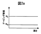
- FIG. 2a shows a doping density profile when doping is performed in a portion where the C / Si ratio is Y
- FIG. 2b shows a portion where the C / Si ratio is smaller than Y (about 0.8 to 0.9) in the same wafer.
- a doping density profile in the case of doping is shown.
- N B1 and N B2 are the residual carrier densities in the respective portions, N B1 is usually about 0.8 to 1 ⁇ 10 15 cm ⁇ 3 and N B2 is about 1 to 3 ⁇ 10 15 cm ⁇ 3 . Therefore , N B1 ⁇ N B2 ⁇ N C. If doping is performed so that N C can be obtained in the portion of FIG.
- N C ⁇ N B1 becomes a doping amount, so that in the portion of FIG. 2 b, N C ⁇ N B1 + N B2 Is the doping value. Therefore, N B2 ⁇ N B1 becomes a doping variation in the portions of FIGS. 2 a and 2 b, which can be a value larger than about 10% of N C. Such a phenomenon occurs because the slope of the graph in FIG.
- the present inventors have used an atomic ratio (C) of carbon and silicon contained in the material gas of the epitaxial film. / Si) between 0.5 and 1.0 and grown (defect reduction layer) and C / Si grown between 1.0 and 1.5 (active layer)
- C atomic ratio
- This method is intended to obtain a triangular epitaxial defect and an epitaxial film with less surface roughness, and teaches a direct means to ensure uniformity of the epitaxial film doping density in the wafer plane. There is no description to do.
- An object of the present invention is to provide an epitaxial SiC single crystal substrate having a high quality epitaxial film excellent in uniformity, and a method for manufacturing the same.
- the inventors of the present invention laminated a plurality of non-doped layers formed without adding an impurity element and a doped layer formed while adding an impurity element during epitaxial growth, and the non-doped layer and the doped layer were formed. It has been found that changing the C / Si ratio during the growth and the thickness thereof are extremely effective in solving the above problems.
- the epitaxial silicon carbide single crystal substrate of the present invention is an epitaxial having a silicon carbide epitaxial film formed by a chemical vapor deposition method on a silicon carbide single crystal substrate having an off angle of 1 ° to 6 °.
- the present invention can include, for example, the following aspects.
- the doped layer is formed with an atomic ratio (C / Si) of carbon and silicon contained in the material gas of the epitaxial film being 1.5 to 2.0, and the non-doped layer is The epitaxial silicon carbide according to (1) above, wherein the atomic ratio (C / Si) of carbon to silicon contained in the material gas of the epitaxial film is 0.5 or more and less than 1.5 Single crystal substrate.
- a method of manufacturing an epitaxial silicon carbide single crystal substrate by forming a silicon carbide epitaxial film by a chemical vapor deposition method on a silicon carbide single crystal substrate having an off angle of 1 ° to 6 °. , Doped layer having a thickness of 0.5 ⁇ m or less formed while adding an impurity element with an atomic ratio (C / Si) of carbon to silicon contained in the material gas of the epitaxial film being 1.5 to 2.0
- Non-doped with a thickness of 0.1 ⁇ m or less formed without adding an impurity element by setting the atomic ratio (C / Si) of carbon and silicon contained in the material gas of the epitaxial film to 0.5 to less than 1.5 A method of manufacturing an epitaxial silicon carbide single crystal substrate, wherein a silicon carbide epitaxial film is formed by alternately growing layers and having two or more doped layers and non-doped layers.
- the present invention it is possible to provide a high-quality epitaxial SiC single crystal substrate that is excellent in in-plane uniformity of doping density in an epitaxial film formed on a substrate having an off angle of 1 ° to 6 °. Is possible.
- the manufacturing method of the present invention uses a CVD method (Chemical Vapor Deposition), an epitaxial structure with an easy apparatus configuration, excellent controllability, and high uniformity and reproducibility can be obtained.
- CVD method Chemical Vapor Deposition
- the device using the epitaxial SiC single crystal substrate of the present invention is formed on a high-quality epitaxial film having excellent in-plane uniformity of the doping density, its characteristics and yield are improved.
- FIG. 3 is a diagram showing an example of a doping density profile when doping is performed in the same place as in FIG. It is an optical microscope photograph which shows an example of the surface state of the film
- An apparatus that can be preferably used for epitaxial growth in the present invention is a horizontal CVD apparatus.
- the CVD method has a simple apparatus configuration and can control growth by turning gas on / off. Therefore, the CVD method is a growth method with excellent controllability and reproducibility of the epitaxial film.
- FIG. 3 shows one mode of a typical growth sequence when performing conventional epitaxial film growth together with the timing of gas introduction.
- a substrate is set in a growth furnace, the inside of the growth furnace is evacuated, and then hydrogen gas is introduced to adjust the pressure to preferably 1 ⁇ 10 4 to 3 ⁇ 10 4 Pa.
- hydrogen gas is introduced to adjust the pressure to preferably 1 ⁇ 10 4 to 3 ⁇ 10 4 Pa.
- the temperature of the growth furnace is raised while keeping the pressure constant, and after reaching a preferable growth temperature of 1550 to 1650 ° C.
- a material gas for example, SiH 4 and C 2 H 4 and doping gas N 2
- SiH 4 flow rate preferably min 40 ⁇ 50cm 3
- C 2 H 4 flow rate is preferably min 20 ⁇ 40 cm 3
- the growth rate is preferably hour 6 ⁇ 7 [mu] m.
- Such a suitable growth rate is determined in consideration of productivity since the film thickness of the epitaxial layer that is normally used is about 10 ⁇ m.
- FIG. 4 shows a preferred example of changes in the C / Si ratio and the N 2 gas flow rate when growth is performed by this conventional method. In the embodiment shown in FIG. 4, the C / Si ratio and the N 2 gas flow rate are not changed from the start to the end of growth.
- the process until the SiC single crystal substrate is set and the growth is started is the same as the embodiment shown in FIG.
- the non-doped layer is grown about 0.1 ⁇ m so that the flow rate ratio of SiH 4 and C 2 H 4 is preferably less than 1.5 in terms of C / Si ratio.
- the flow rate ratio between SiH 4 and C 2 H 4 is a C / Si ratio, preferably 1.5 or more, and preferably about 0.2 ⁇ m.
- nitrogen as a doping gas is introduced. To make a doped layer.
- the non-doped layer and the doped layer are repeatedly grown, and the introduction of SiH 4 , C 2 H 4 and N 2 is stopped when a desired film thickness is obtained.
- the subsequent procedure is the same as in FIG.
- An example of changes in the C / Si ratio and the N 2 gas flow rate in the embodiment of FIG. 5 is shown in FIG. In this way, by doping a non-doped layer with a low C / Si ratio and growing a doped layer with a high C / Si ratio, doping can be performed in a state where site-competition hardly occurs. It becomes possible.
- the thickness of the non-doped layer is reduced as a whole, the above-described in-plane non-uniformity of the doping density can also be suppressed. This will be described with reference to FIG. 7 with an example.
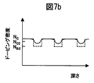
- FIG. 7a is an example of a doping profile when doping is performed by applying the present invention in the same place as in FIG. 2a.
- the doping density becomes a dotted line. That is, in the doped layer formed while introducing nitrogen as a doping gas, the C / Si ratio is higher than the value Y in FIG. 1 and is 1.5 or more, so that N is not affected by the residual carrier density. Doping is performed to obtain C.
- the C / Si ratio is the value Y in FIG. 1 (preferably about 1.0), so that the residual carrier density of N B1 in FIG. Will come to show.
- the profile becomes a solid line.
- the effective doping density is considered to be about N C1 .
- FIG. 7b is the same place as FIG. 2b, and the dotted line shows an ideal doping profile as in FIG. 7a.
- the C / Si ratio is higher than the value Y in FIG. 1 (for example, the C / Si ratio is 1.5 or more)
- the N C value of the doped layer is not affected by the residual impurities. It becomes similar to N C.
- the residual carrier density of the non-doped layer in which the C / Si ratio is smaller than the value Y in FIG. 1 for example, 0.8 to 0.9
- the residual impurity density is high.
- N B2 the effective doping density is considered to be about NC2 . Therefore, the difference between N C1 and N C2 is reduced, and the in-plane uniformity of the doping density is improved.
- a good epitaxial film with high in-plane doping uniformity can be obtained, but it is grown at a low C / Si ratio. Since the non-doped layer is essential for growth on a substrate having a small off angle, if it is too thin, an epitaxial defect or the like may occur and the film quality may deteriorate. On the other hand, if it is too thick, it may adversely affect the in-plane uniformity of the entire doping density, and there may be a problem that the resistance becomes high in a current device in which current flows perpendicularly to the substrate.
- the doped layer grown at a high C / Si ratio is thinner than the non-doped layer, the contribution to the improvement of the in-plane uniformity of the doping density may be small, and if it is too thick, the film quality may be deteriorated. .
- the thickness of the non-doped layer is preferably 0.1 ⁇ m or less, more preferably 0.05 to 0.1 ⁇ m. .
- the thickness of the doped layer is preferably 0.5 ⁇ m or less, and more preferably 0.2 to 0.5 ⁇ m.
- the ratio of the thickness of the doped layer to the non-doped layer is preferably about 2 to 10.
- each of the doped layer and the non-doped layer is made to have two or more layers. However, the more the number of laminations of the non-doped layer and the doped layer, the more the doping density is averaged over the entire epitaxial film, and the in-plane uniformity is improved.
- the number of laminations of the non-doped layer and the doped layer is preferably more than about 20 times, more preferably about 20 to 40 times. is there.
- a low C / Si ratio that is, a non-doped layer is necessary when starting growth on a SiC substrate because growth is performed on a substrate having a small off angle.
- the outermost surface is a part that contacts the electrode of the device, a doped layer is necessary.
- the C / Si ratio when growing the non-doped layer is preferably 0.5 or more and less than 1.5 in consideration of the growth on the low off-angle substrate.
- the C / Si ratio is less than 0.5, defects called Si droplets in which excessive Si atoms condense on the substrate surface tend to be formed.
- the C / Si ratio is 1.5 or more, surface roughness and epitaxial defects tend to increase. More preferably, the C / Si ratio in this case is 0.8 to 1.2.
- the C / Si ratio when growing the doped layer is too low, the effect of site-competition tends to appear.
- the C / Si ratio is too high, epitaxial defects such as triangular defects tend to increase.
- the C / Si ratio in this case is preferably 1.5 or more and 2.0 or less, and more preferably 1.5 to 1.8.
- the doping atom number density of the doped layer is preferably larger than N B1 and N B2 from FIGS. 7a and 7b, and for that purpose, 1 ⁇ 10 15 cm ⁇ 3 or more is preferable. Since surface roughness may occur when the doping atom number density is too high, it is more preferably 1 ⁇ 10 15 cm ⁇ 3 or more and 1 ⁇ 10 17 cm ⁇ 3 or less.
- the total thickness of the epitaxial film is preferably 5 ⁇ m or more and 50 ⁇ m or less in consideration of the breakdown voltage of a device that is normally formed, the productivity of the epitaxial film, and the like. More preferably, it is 10 to 20 ⁇ m.
- the off angle of the substrate is 1 ° or more and 6 ° or less. If the substrate is less than 1 °, the off angle is too small, and the effects of the present invention may not be sufficiently exhibited. On the other hand, if the off-angle of the substrate exceeds 6 °, the substrate can be grown with a high C / Si ratio, and the in-plane uniformity may be improved without using the present invention.
- the present invention when an epitaxial film is grown on a SiC single crystal substrate, a plurality of non-doped layers and doped layers are stacked, and the C / Si ratio and thickness when growing the non-doped layers and doped layers are increased.
- the thickness By changing the thickness, the in-plane uniformity of the doping density can be reduced to 5% or less in terms of ⁇ / mean.
- FIG. 1 As can be seen from FIG.
- Ohmic electrodes are formed on the front surface and the back surface of the substrate, and the current value between the electrodes is regarded as equivalent to the doping density, and the in-plane uniformity is evaluated.
- an ohmic electrode is made of Ni on the entire back surface, and a Ni ohmic electrode of about 200 ⁇ m square is also made on the front surface. A voltage is applied to the ohmic electrodes on the front and back surfaces, and for example, the current value when 10 V is applied is measured.
- the impurity element added when forming the epitaxial film in the present invention has been described mainly using nitrogen as an example in the above-described embodiment.
- nitrogen for example, aluminum or the like is used as an impurity to form a doped layer. It may be.
- the material gas of the epitaxial film SiH 4 and C 2 H 4 have been described as examples in the above-described embodiment, but it is needless to say that other silicon sources and carbon sources may be used.
- Examples of devices suitably formed on the substrate of the present invention having an epitaxial film grown in this way include Schottky barrier diodes, PIN diodes, MOS diodes, MOS transistors, and the like. From the viewpoint of taking advantage of low loss, a device used for power control is a suitable example for the substrate of the present invention.
- the lattice constants of the respective layers are different, so that distortion occurs at the interface and the basal plane dislocation from the substrate is converted into edge dislocation. Will increase. Therefore, the basal plane dislocation density existing on the surface of the epitaxial film thus grown can be expected to be 20 pieces / cm 2 or less. Further, since the dislocation density is reduced and the film quality is improved, it is expected that the n value indicating the performance of the diode when the Schottky barrier diode is formed is also about 1.01 to 1.03.
- Example 1 A SiC single crystal substrate having a 4H type polytype was prepared by slicing a SiC single crystal ingot for a 3-inch (76 mm) wafer at a thickness of about 400 ⁇ m, performing rough cutting and normal polishing with diamond abrasive grains. This substrate was n-type and had a resistivity of about 0.02 ⁇ ⁇ cm. Epitaxial growth was performed on the Si surface of the substrate. The off angle of the substrate is 4 °. The growth procedure was as follows. After setting the substrate in the growth furnace and evacuating the inside of the growth furnace, the pressure was adjusted to 1.0 ⁇ 10 4 Pa while introducing 150 L of hydrogen gas per minute. Thereafter, the temperature of the growth furnace is raised to 1600 ° C.
- the SiH 4 flow rate is 40 cm 3 / min
- the C 2 H 4 flow rate is 22 cm 3 / min (C / Si ratio 1.1).
- Started growing After growing the non-doped layer by 0.1 ⁇ m, the SiH 4 flow rate is 40 cm 3 / min, the C 2 H 4 flow rate is 30 cm 3 / min (C / Si ratio 1.5), and the N 2 flow rate, which is a doping gas, is further increased.
- the doping layer was grown by 0.2 ⁇ m at a rate of 30 cm 3 / min (doping atom number density 1 ⁇ 10 16 cm ⁇ 3 ).
- the introduction of N 2 was stopped, the non-doped layer was grown again by 0.1 ⁇ m, the N 2 flow rate was increased to 30 cm 3 per minute, and the doped layer was grown by 0.2 ⁇ m. Each of the doped layers was grown a total of 30 times so that the uppermost layer was a doped layer.
- FIG. 8 An optical micrograph of the film epitaxially grown in this way is shown in FIG. FIG. 8 shows that a good film with less surface roughness and defects is obtained.
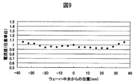
- FIG. 9 shows the result of forming an ohmic electrode of Ni on this epitaxial film and evaluating the doping density based on the current value. The uniformity was good, and the in-plane uniformity expressed by ⁇ / mean was 4.5%.
- Example 2 Epitaxial growth was performed on the Si surface of a 3 inch (76 mm) SiC single crystal substrate having a 4H-type polytype, which was sliced, roughly ground, and normally polished in the same manner as in Example 1. The off angle of the substrate is 4 °. This substrate was n-type and had a resistivity of about 0.02 ⁇ ⁇ cm. The procedure up to the start of growth, temperature, and the like were the same as in Example 1. The growth procedure in this example was as follows. The growth of the non-doped layer was started at a SiH 4 flow rate of 40 cm 3 / min and a C 2 H 4 flow rate of 22 cm 3 / min (C / Si ratio 1.1).
- the flow rate of SiH 4 is set to 40 cm 3 / min
- the flow rate of C 2 H 4 is set to 30 cm 3 / min (C / Si ratio 1.5)
- the flow rate of N 2 as a doping gas is further increased.
- the doped layer was grown to 0.5 ⁇ m at a density of 3 cm 3 / min (doping atom number density 1 ⁇ 10 15 cm ⁇ 3 ).
- the introduction of N 2 was stopped, the non-doped layer was grown again by 0.05 ⁇ m, the N 2 flow rate was 3 cm 3 per minute, and the doped layer was grown by 0.5 ⁇ m.
- Each of the doped layers was grown 20 times in total.
- the film epitaxially grown in this way was a good film with less surface roughness and defects, and the in-plane uniformity ⁇ / mean evaluated by the current value was 3.5%.
- Example 3 Epitaxial growth was performed on the Si surface of a 3 inch (76 mm) SiC single crystal substrate having a 4H-type polytype, which was sliced, roughly ground, and normally polished in the same manner as in Example 1. The off angle of the substrate is 4 °. This substrate was n-type and had a resistivity of about 0.02 ⁇ ⁇ cm. The procedure up to the start of growth, temperature, and the like were the same as in Example 1. The growth procedure in this example was as follows. The growth of the non-doped layer was started at a SiH 4 flow rate of 40 cm 3 / min and a C 2 H 4 flow rate of 10 cm 3 / min (C / Si ratio 0.5).
- the non-doped layer was 0.1 ⁇ m grown, the SiH 4 min flow rate 40cm 3, C 2 H 4 per minute flow rate 40cm 3 (C / Si ratio 2.0), the N 2 flow rate is more doping gas
- the doped layer was grown by 0.2 ⁇ m at a rate of 30 cm 3 / min (doping atom number density 1 ⁇ 10 16 cm ⁇ 3 ). Thereafter, the introduction of N 2 was stopped, the non-doped layer was grown again by 0.1 ⁇ m, and the doped layer was further grown by 0.2 ⁇ m at an N 2 flow rate of 30 cm 3 per minute. Thereafter, in this way, the non-doped layer and the doped layer were each grown 30 times in total.
- the film epitaxially grown in this way was a good film with less surface roughness and defects, and the in-plane uniformity ⁇ / mean evaluated by the current value was 4.7%.
- Example 4 Epitaxial growth was performed on the Si surface of a 3 inch (76 mm) SiC single crystal substrate having a 4H-type polytype, which was sliced, roughly ground, and normally polished in the same manner as in Example 1. The off angle of the substrate is 4 °. This substrate was n-type and had a resistivity of about 0.02 ⁇ ⁇ cm. The procedure up to the start of growth, temperature, and the like were the same as in Example 1. The growth procedure in this example was as follows. The growth of the non-doped layer was started at a SiH 4 flow rate of 40 cm 3 / min and a C 2 H 4 flow rate of 10 cm 3 / min (C / Si ratio 0.5).
- the non-doped layer is 0.05 ⁇ m grown, the SiH 4 min flow rate 40cm 3, C 2 H 4 per minute flow rate 40cm 3 (C / Si ratio 2.0), the N 2 flow rate is more doping gas
- the doped layer was grown to 0.5 ⁇ m at a rate of 300 cm 3 / min (doping atom number density 1 ⁇ 10 17 cm ⁇ 3 ). Thereafter, the introduction of N 2 was stopped, the non-doped layer was grown again by 0.05 ⁇ m, and the N 2 flow rate was 300 cm 3 per minute to grow the doped layer by 0.5 ⁇ m. Thereafter, in this manner, the non-doped layer and the doped layer were grown 20 times in total.
- the film epitaxially grown in this way was a good film with less surface roughness and defects, and the in-plane uniformity ⁇ / mean evaluated by the current value was 4.0%.
- Example 5 Epitaxial growth was performed on the Si surface of a 3 inch (76 mm) SiC single crystal substrate having a 4H-type polytype, which was sliced, roughly ground, and normally polished in the same manner as in Example 1. The off angle of the substrate is 1 °. This substrate was n-type and had a resistivity of about 0.02 ⁇ ⁇ cm. The procedure up to the start of growth, temperature, and the like were the same as in Example 1. The growth procedure in this example was as follows. The growth of the non-doped layer was started at a SiH 4 flow rate of 40 cm 3 / min and a C 2 H 4 flow rate of 10 cm 3 / min (C / Si ratio 0.5).
- the SiH 4 flow rate is 40 cm 3 / min
- the C 2 H 4 flow rate is 30 cm 3 / min (C / Si ratio 1.5)
- the N 2 flow rate which is a doping gas, is further increased.
- the doped layer was grown by 0.2 ⁇ m at a rate of 30 cm 3 per minute (doping atom number density 1 ⁇ 10 16 cm ⁇ 3 ). Thereafter, the introduction of N 2 was stopped, the non-doped layer was grown again by 0.1 ⁇ m, and the doped layer was further grown by 0.2 ⁇ m at an N 2 flow rate of 30 cm 3 per minute.
- the non-doped layer and the doped layer were each grown 30 times in total.
- the film epitaxially grown in this way was a good film with few surface roughness and defects, and ⁇ / mean of in-plane uniformity evaluated by current value was 4.8%.
- Example 6 Epitaxial growth was performed on the Si surface of a 3 inch (76 mm) SiC single crystal substrate having a 4H-type polytype, which was sliced, roughly ground, and normally polished in the same manner as in Example 1. The off angle of the substrate is 6 °. This substrate was n-type and had a resistivity of about 0.02 ⁇ ⁇ cm. The procedure up to the start of growth, temperature, and the like were the same as in Example 1. The growth procedure in this example was as follows. The growth of the non-doped layer was started at a SiH 4 flow rate of 40 cm 3 / min and a C 2 H 4 flow rate of 22 cm 3 / min (C / Si ratio 1.1).
- the SiH 4 flow rate is 40 cm 3 / min
- the C 2 H 4 flow rate is 30 cm 3 / min (C / Si ratio 1.5)
- the N 2 flow rate which is a doping gas, is further increased.
- the doped layer was grown by 0.2 ⁇ m at a rate of 30 cm 3 per minute (doping atom number density 1 ⁇ 10 16 cm ⁇ 3 ). Thereafter, the introduction of N 2 was stopped, the non-doped layer was grown again by 0.1 ⁇ m, and the doped layer was further grown by 0.2 ⁇ m at an N 2 flow rate of 30 cm 3 per minute.
- the non-doped layer and the doped layer were each grown 30 times in total.
- the film epitaxially grown in this way was a good film with less surface roughness and defects, and the in-plane uniformity ⁇ / mean evaluated by the current value was 4.2%.
- Comparative Example 1 As a comparative example, epitaxial growth was performed on the Si surface of a 3 inch (76 mm) SiC single crystal substrate having a 4H-type polytype that was sliced, roughly cut, and normally polished as in Example 1. The off angle of the substrate is 4 °. The procedure up to the start of growth, temperature, and the like are the same as in Example 1, but the growth is 40 cm 3 per minute for the SiH 4 flow rate and 22 cm 3 per minute for the C 2 H 4 flow rate (C / Si ratio 1.1). Further, the flow rate of N 2 as a doping gas was 1 cm 3 (doping atom number density 1 ⁇ 10 16 cm ⁇ 3 ), and a doped layer was grown by 10 ⁇ m. The film epitaxially grown in this way is a good film with less surface roughness and defects, but the in-plane uniformity ⁇ / mean evaluated by the current value was 15%.
- the epitaxial SiC single crystal substrate which has a high quality epitaxial film excellent in the in-plane uniformity of doping density in the epitaxial growth on a SiC single crystal substrate. Therefore, if an electronic device is formed on such a substrate, it can be expected that the characteristics and yield of the device are improved.
- SiH 4 and C 2 H 4 are used as the material gas, but the same applies to the case where trichlorosilane is used as the Si source and C 3 H 8 is used as the C source.
Landscapes
- Chemical & Material Sciences (AREA)
- Engineering & Computer Science (AREA)
- Materials Engineering (AREA)
- Metallurgy (AREA)
- Organic Chemistry (AREA)
- Crystallography & Structural Chemistry (AREA)
- Chemical Kinetics & Catalysis (AREA)
- General Chemical & Material Sciences (AREA)
- Inorganic Chemistry (AREA)
- Mechanical Engineering (AREA)
- Crystals, And After-Treatments Of Crystals (AREA)
- Chemical Vapour Deposition (AREA)
Abstract
Description
本発明は、例えば、以下の態様を含むことができる。
(1)オフ角度が1°以上6°以下である炭化珪素単結晶基板上に、化学気相堆積法によって形成された炭化珪素エピタキシャル膜を有するエピタキシャル炭化珪素単結晶基板であって、
該エピタキシャル膜が、不純物元素を添加しながら形成した厚さ0.5μm以下のドープ層と、不純物元素を添加せずに形成した厚さ0.1μm以下のノンドープ層とを交互に積層して、ドープ層及びノンドープ層をそれぞれ2層以上有してなることを特徴とするエピタキシャル炭化珪素単結晶基板。
(2)前記ドープ層が、エピタキシャル膜の材料ガス中に含まれる炭素と珪素の原子数比(C/Si)を1.5以上2.0以下にして形成され、また、前記ノンドープ層が、エピタキシャル膜の材料ガス中に含まれる炭素と珪素の原子数比(C/Si)を0.5以上1.5未満にして形成されたことを特徴とする上記(1)に記載のエピタキシャル炭化珪素単結晶基板。
(3)前記ドープ層の厚さが前記ノンドープ層の厚さよりも大きいことを特徴とする上記(1)又は(2)に記載のエピタキシャル炭化珪素単結晶基板。
(4)前記ドープ層のドーピング原子数密度が1×1015cm−3以上であることを特徴とする上記(1)~(3)のいずれかに記載のエピタキシャル炭化珪素単結晶基板。
(5)オフ角度が1°以上6°以下である炭化珪素単結晶基板上に、化学気相堆積法によって炭化珪素エピタキシャル膜を形成して、エピタキシャル炭化珪素単結晶基板を製造する方法であって、
エピタキシャル膜の材料ガス中に含まれる炭素と珪素の原子数比(C/Si)を1.5以上2.0以下にして、不純物元素を添加しながら形成する厚さ0.5μm以下のドープ層と、
エピタキシャル膜の材料ガス中に含まれる炭素と珪素の原子数比(C/Si)を0.5以上1.5未満にして、不純物元素を添加せずに形成する厚さ0.1μm以下のノンドープ層と、を交互に成長させて、ドープ層及びノンドープ層をそれぞれ2層以上有するようにして炭化珪素エピタキシャル膜を形成することを特徴とするエピタキシャル炭化珪素単結晶基板の製造方法。
まず、SiC単結晶基板上へのエピタキシャル成長について述べる。
本発明で好適にエピタキシャル成長に使用可能な装置は、横型のCVD装置である。CVD法は、装置構成が簡単であり、ガスのon/offで成長を制御できるため、エピタキシャル膜の制御性、再現性に優れた成長方法である。
このような好適な成長速度は、通常利用されるエピタキシャル層の膜厚が10μm程度であるため、生産性を考慮して決定されたものである。
一定時間成長し、所望の膜厚が得られた時点で材料ガス(すなわち、上記したSiH4、C2H4およびN2)の導入を止め、水素ガスのみ流した状態で温度を下げる。
温度が常温まで下がった後、水素ガスの導入を止め、成長室内を真空排気し、不活性ガスを成長室に導入して、成長室を大気圧に戻してから、基板を取り出す。
この従来方式で成長を行う場合のC/Si比とN2ガス流量の変化の好適な一例を図4に示す。この図4に示した態様においては、成長開始から終了までC/Si比とN2ガス流量は変化させず、一定である。
その後は、ノンドープ層とドープ層を繰り返し成長させて、所望の膜厚が得られた時点でSiH4、C2H4およびN2の導入を止める。その後の手順は、図3の場合と同様である。
この図5の態様におけるC/Si比とN2ガス流量の変化の一例を図6に示す。このように、低いC/Si比でノンドープ層を成長させ、高いC/Si比でドープ層を成長させることにより、site−competitionが起こりにくい状態でドーピングが行えるため、制御性に優れたドーピングが可能になる。さらに、本発明では、ノンドープ層の厚さを全体的に薄くするため、前述したドーピング密度の面内不均一性も抑制することができる。この点について、図7を用いて、下記で一例を挙げながら説明する。
一方、ドーピングガスである窒素を導入せずに形成するノンドープ層では、C/Si比が図1における値Y(好ましくは、1.0程度)であるため、図2aのNB1の残留キャリア密度を示すようになる。しかし実際には、ドープ層とノンドープ層の間のドーピング密度変化は連続的であるため、実線のようなプロファイルになる。そして、実効的なドーピング密度はNC1程度と考えられる。
ノンドープ層とドープ層の積層順番に関しては、SiC基板上に成長を開始する時は、小さいオフ角を持つ基板上の成長になるため、低いC/Si比、すなわちノンドープ層が必要である。一方、最表面は、デバイスの電極と接触する部分であるため、ドープ層が必要である。
一方、ドープ層を成長する時のC/Si比は、低すぎるとsite−competitionの影響が現れ易い傾向がある。他方、C/Si比が高すぎると三角形欠陥等のエピタキシャル欠陥が増加する傾向がある。このため、この場合のC/Si比は、1.5以上2.0以下が好適であり、より好適には1.5~1.8である。さらに、ドープ層のドーピング原子数密度は、図7a、図7bより、NB1およびNB2より大きい事が好ましく、そのためには1×1015cm−3以上が好ましい。ドーピング原子数密度が高すぎると表面荒れが生じる可能性があるため、より好適には1×1015cm−3以上1×1017cm−3以下である。
3インチ(76mm)ウェーハ用SiC単結晶インゴットから、約400μmの厚さでスライスし、粗削りとダイヤモンド砥粒による通常研磨を実施して、4H型のポリタイプを有するSiC単結晶基板を用意した。この基板はn型であり、抵抗率は約0.02Ω・cmであった。
この基板のSi面に、エピタキシャル成長を実施した。基板のオフ角は4°である。成長の手順は、以下の通りであった。
成長炉に基板をセットし、成長炉内を真空排気した後、水素ガスを毎分150L導入しながら圧力を1.0×10⁴Paに調整した。その後、圧力を一定に保ちながら成長炉の温度を1600℃まで上げ、SiH4流量を毎分40cm3、C2H4流量を毎分22cm3(C/Si比1.1)にしてノンドープ層の成長を開始した。
ノンドープ層を0.1μm成長させた後、SiH4流量を毎分40cm3、C2H4流量を毎分30cm3(C/Si比1.5)にし、さらにドーピングガスであるN2流量を毎分30cm3にして(ドーピング原子数密度1×1016cm−3)、ドープ層を0.2μm成長させた。
その後、N2の導入を止め、再びノンドープ層を0.1μm成長させて、更に、N2流量を毎分30cm3にしてドープ層を0.2μm成長させて、以降このようにして、ノンドープ層とドープ層をそれぞれ合計30回成長させ、最上層がドープ層となるようにした。
実施例1と同様にスライス、粗削り、通常研磨を行った、4H型のポリタイプを有する3インチ(76mm)のSiC単結晶基板のSi面に、エピタキシャル成長を実施した。基板のオフ角は4°である。この基板はn型であり、抵抗率は約0.02Ω・cmであった。
成長開始までの手順、温度等は、実施例1と同様であった。本実施例における成長の手順は、以下の通りであった。
SiH4流量を毎分40cm3、C2H4流量を毎分22cm3(C/Si比1.1)にしてノンドープ層の成長を開始した。ノンドープ層を0.05μm成長させた後、SiH4流量を毎分40cm3、C2H4流量を毎分30cm3(C/Si比1.5)にし、さらにドーピングガスであるN2流量を毎分3cm3にして(ドーピング原子数密度1×1015cm−3)、ドープ層を0.5μm成長させた。
その後、N2の導入を止め、再びノンドープ層を0.05μm成長させて、更に、N2流量を毎分3cm3にしてドープ層を0.5μm成長させて、以降このようにして、ノンドープ層とドープ層をそれぞれ合計20回成長させた。このようにしてエピタキシャル成長を行った膜は、表面荒れや欠陥の少ない良好な膜であり、電流値で評価した面内均一性のσ/meanは3.5%であった。
実施例1と同様にスライス、粗削り、通常研磨を行った、4H型のポリタイプを有する3インチ(76mm)のSiC単結晶基板のSi面に、エピタキシャル成長を実施した。基板のオフ角は4°である。この基板はn型であり、抵抗率は約0.02Ω・cmであった。
成長開始までの手順、温度等は、実施例1と同様であった。本実施例における成長の手順は、以下の通りであった。
SiH4流量を毎分40cm3、C2H4流量を毎分10cm3(C/Si比0.5)にしてノンドープ層の成長を開始した。ノンドープ層を0.1μm成長させた後、SiH4流量を毎分40cm3、C2H4流量を毎分40cm3(C/Si比2.0)にし、さらにドーピングガスであるN2流量を毎分30cm3(ドーピング原子数密度1×1016cm−3)にしてドープ層を0.2μm成長させた。
その後、N2の導入を止め、再びノンドープ層を0.1μm成長させて、更に、N2流量を毎分30cm3にしてドープ層を0.2μm成長させた。以降このようにして、ノンドープ層とドープ層をそれぞれ合計30回成長させた。
このようにしてエピタキシャル成長を行った膜は、表面荒れや欠陥の少ない良好な膜であり、電流値で評価した面内均一性のσ/meanは4.7%であった。
実施例1と同様にスライス、粗削り、通常研磨を行った、4H型のポリタイプを有する3インチ(76mm)のSiC単結晶基板のSi面に、エピタキシャル成長を実施した。基板のオフ角は4°である。この基板はn型であり、抵抗率は約0.02Ω・cmであった。
成長開始までの手順、温度等は、実施例1と同様であった。本実施例における成長の手順は、以下の通りであった。
SiH4流量を毎分40cm3、C2H4流量を毎分10cm3(C/Si比0.5)にしてノンドープ層の成長を開始した。ノンドープ層を0.05μm成長させた後、SiH4流量を毎分40cm3、C2H4流量を毎分40cm3(C/Si比2.0)にし、さらにドーピングガスであるN2流量を毎分300cm3(ドーピング原子数密度1×1017cm−3)にして、ドープ層を0.5μm成長させた。
その後、N2の導入を止め、再びノンドープ層を0.05μm成長させて、更に、N2流量を毎分300cm3にしてドープ層を0.5μm成長させた。以降このようにして、ノンドープ層とドープ層をそれぞれ合計20回成長させた。
このようにしてエピタキシャル成長を行った膜は、表面荒れや欠陥の少ない良好な膜であり、電流値で評価した面内均一性のσ/meanは4.0%であった。
実施例1と同様にスライス、粗削り、通常研磨を行った、4H型のポリタイプを有する3インチ(76mm)のSiC単結晶基板のSi面に、エピタキシャル成長を実施した。基板のオフ角は1°である。この基板はn型であり、抵抗率は約0.02Ω・cmであった。
成長開始までの手順、温度等は、実施例1と同様であった。本実施例における成長の手順は、以下の通りであった。
SiH4流量を毎分40cm3、C2H4流量を毎分10cm3(C/Si比0.5)にしてノンドープ層の成長を開始した。ノンドープ層を0.1μm成長させた後、SiH4流量を毎分40cm3、C2H4流量を毎分30cm3(C/Si比1.5)にし、さらにドーピングガスであるN2流量を毎分30cm3(ドーピング原子数密度1×1016cm−3)にして、ドープ層を0.2μm成長させた。
その後、N2の導入を止め、再びノンドープ層を0.1μm成長させて、更に、N2流量を毎分30cm3にしてドープ層を0.2μm成長させた。以降このようにして、ノンドープ層とドープ層をそれぞれ合計30回成長させた。
このようにしてエピタキシャル成長を行った膜は、表面荒れや欠陥の少ない良好な膜であり、電流値で評価した面内均一性のσ/meanは4.8%であった。
実施例1と同様にスライス、粗削り、通常研磨を行った、4H型のポリタイプを有する3インチ(76mm)のSiC単結晶基板のSi面に、エピタキシャル成長を実施した。基板のオフ角は6°である。この基板はn型であり、抵抗率は約0.02Ω・cmであった。
成長開始までの手順、温度等は、実施例1と同様であった。本実施例における成長の手順は、以下の通りであった。
SiH4流量を毎分40cm3、C2H4流量を毎分22cm3(C/Si比1.1)にしてノンドープ層の成長を開始した。ノンドープ層を0.1μm成長させた後、SiH4流量を毎分40cm3、C2H4流量を毎分30cm3(C/Si比1.5)にし、さらにドーピングガスであるN2流量を毎分30cm3(ドーピング原子数密度1×1016cm−3)にして、ドープ層を0.2μm成長させた。
その後、N2の導入を止め、再びノンドープ層を0.1μm成長させて、更に、N2流量を毎分30cm3にしてドープ層を0.2μm成長させた。以降このようにして、ノンドープ層とドープ層をそれぞれ合計30回成長させた。
このようにしてエピタキシャル成長を行った膜は、表面荒れや欠陥の少ない良好な膜であり、電流値で評価した面内均一性のσ/meanは4.2%であった。
比較例として、実施例1と同様にスライス、粗削り、通常研磨を行った、4H型のポリタイプを有する3インチ(76mm)のSiC単結晶基板のSi面に、エピタキシャル成長を実施した。基板のオフ角は4°である。
成長開始までの手順、温度等は、実施例1と同様であるが、成長は、SiH4流量を毎分40cm3、C2H4流量を毎分22cm3(C/Si比1.1)にし、さらにドーピングガスであるN2流量を1cm3(ドーピング原子数密度1×1016cm−3)にして、ドープ層を10μm成長した。
このようにしてエピタキシャル成長を行った膜は、表面荒れや欠陥の少ない良好な膜であるが、電流値で評価した面内均一性のσ/meanは15%であった。
Claims (5)
- オフ角度が1°以上6°以下である炭化珪素単結晶基板上に、化学気相堆積法によって形成された炭化珪素エピタキシャル膜を有するエピタキシャル炭化珪素単結晶基板であって、
該エピタキシャル膜が、不純物元素を添加しながら形成した厚さ0.5μm以下のドープ層と、不純物元素を添加せずに形成した厚さ0.1μm以下のノンドープ層とを交互に積層して、ドープ層及びノンドープ層をそれぞれ2層以上有してなることを特徴とするエピタキシャル炭化珪素単結晶基板。 - 前記ドープ層が、エピタキシャル膜の材料ガス中に含まれる炭素と珪素の原子数比(C/Si)を1.5以上2.0以下にして形成され、また、前記ノンドープ層が、エピタキシャル膜の材料ガス中に含まれる炭素と珪素の原子数比(C/Si)を0.5以上1.5未満にして形成されたことを特徴とする請求項1に記載のエピタキシャル炭化珪素単結晶基板。
- 前記ドープ層の厚さが前記ノンドープ層の厚さよりも大きいことを特徴とする請求項1又は2に記載のエピタキシャル炭化珪素単結晶基板。
- 前記ドープ層のドーピング原子数密度が1×1015cm−3以上であることを特徴とする請求項1又は2に記載のエピタキシャル炭化珪素単結晶基板。
- オフ角度が1°以上6°以下である炭化珪素単結晶基板上に、化学気相堆積法によって炭化珪素エピタキシャル膜を形成して、エピタキシャル炭化珪素単結晶基板を製造する方法であって、
エピタキシャル膜の材料ガス中に含まれる炭素と珪素の原子数比(C/Si)を1.5以上2.0以下にして、不純物元素を添加しながら形成する厚さ0.5μm以下のドープ層と、
エピタキシャル膜の材料ガス中に含まれる炭素と珪素の原子数比(C/Si)を0.5以上1.5未満にして、不純物元素を添加せずに形成する厚さ0.1μm以下のノンドープ層と、を交互に成長させて、
ドープ層及びノンドープ層をそれぞれ2層以上有するようにして炭化珪素エピタキシャル膜を形成することを特徴とするエピタキシャル炭化珪素単結晶基板の製造方法。
Priority Applications (4)
| Application Number | Priority Date | Filing Date | Title |
|---|---|---|---|
| KR1020127025335A KR101430217B1 (ko) | 2010-05-11 | 2011-05-10 | 에피택셜 탄화규소 단결정 기판 및 그 제조 방법 |
| US13/697,211 US8901570B2 (en) | 2010-05-11 | 2011-05-10 | Epitaxial silicon carbide single crystal substrate and process for producing the same |
| CN201180018417.5A CN102844474B (zh) | 2010-05-11 | 2011-05-10 | 外延碳化硅单晶基板及其制造方法 |
| EP11780725.5A EP2570522B1 (en) | 2010-05-11 | 2011-05-10 | Epitaxial silicon carbide single-crystal substrate and method for producing the same |
Applications Claiming Priority (2)
| Application Number | Priority Date | Filing Date | Title |
|---|---|---|---|
| JP2010-109105 | 2010-05-11 | ||
| JP2010109105A JP4880052B2 (ja) | 2010-05-11 | 2010-05-11 | エピタキシャル炭化珪素単結晶基板及びその製造方法 |
Publications (1)
| Publication Number | Publication Date |
|---|---|
| WO2011142470A1 true WO2011142470A1 (ja) | 2011-11-17 |
Family
ID=44914519
Family Applications (1)
| Application Number | Title | Priority Date | Filing Date |
|---|---|---|---|
| PCT/JP2011/061124 Ceased WO2011142470A1 (ja) | 2010-05-11 | 2011-05-10 | エピタキシャル炭化珪素単結晶基板及びその製造方法 |
Country Status (6)
| Country | Link |
|---|---|
| US (1) | US8901570B2 (ja) |
| EP (1) | EP2570522B1 (ja) |
| JP (1) | JP4880052B2 (ja) |
| KR (1) | KR101430217B1 (ja) |
| CN (1) | CN102844474B (ja) |
| WO (1) | WO2011142470A1 (ja) |
Cited By (5)
| Publication number | Priority date | Publication date | Assignee | Title |
|---|---|---|---|---|
| US20140117381A1 (en) * | 2012-10-31 | 2014-05-01 | Lg Innotek Co., Ltd. | Epitaxial Wafer, Method for Fabricating the Same, and Semiconductor Device Including the Same |
| WO2015129876A1 (ja) * | 2014-02-27 | 2015-09-03 | 京セラ株式会社 | 炭化珪素の結晶のインゴット、炭化珪素のウェハ、炭化珪素の結晶のインゴットおよび炭化珪素のウェハの製造方法 |
| WO2015170500A1 (ja) * | 2014-05-08 | 2015-11-12 | 三菱電機株式会社 | SiCエピタキシャルウエハおよび炭化珪素半導体装置の製造方法 |
| WO2017043165A1 (ja) * | 2015-09-11 | 2017-03-16 | 住友電気工業株式会社 | 炭化珪素エピタキシャル基板および炭化珪素半導体装置の製造方法 |
| JP2017059670A (ja) * | 2015-09-16 | 2017-03-23 | ローム株式会社 | SiCエピタキシャルウェハ、SiCエピタキシャルウェハの製造装置、SiCエピタキシャルウェハの製造方法、および半導体装置 |
Families Citing this family (31)
| Publication number | Priority date | Publication date | Assignee | Title |
|---|---|---|---|---|
| KR101926694B1 (ko) * | 2012-05-30 | 2018-12-07 | 엘지이노텍 주식회사 | 탄화규소 에피 웨이퍼 및 이의 제조 방법 |
| KR101926678B1 (ko) * | 2012-05-31 | 2018-12-11 | 엘지이노텍 주식회사 | 탄화규소 에피 웨이퍼 및 이의 제조 방법 |
| US8860040B2 (en) | 2012-09-11 | 2014-10-14 | Dow Corning Corporation | High voltage power semiconductor devices on SiC |
| US9018639B2 (en) | 2012-10-26 | 2015-04-28 | Dow Corning Corporation | Flat SiC semiconductor substrate |
| US9017804B2 (en) | 2013-02-05 | 2015-04-28 | Dow Corning Corporation | Method to reduce dislocations in SiC crystal growth |
| US9797064B2 (en) | 2013-02-05 | 2017-10-24 | Dow Corning Corporation | Method for growing a SiC crystal by vapor deposition onto a seed crystal provided on a support shelf which permits thermal expansion |
| US9738991B2 (en) | 2013-02-05 | 2017-08-22 | Dow Corning Corporation | Method for growing a SiC crystal by vapor deposition onto a seed crystal provided on a supporting shelf which permits thermal expansion |
| US8940614B2 (en) | 2013-03-15 | 2015-01-27 | Dow Corning Corporation | SiC substrate with SiC epitaxial film |
| JP6289952B2 (ja) | 2014-03-19 | 2018-03-07 | 株式会社東芝 | SiCエピタキシャル基板の製造方法、半導体装置の製造方法 |
| JP6306411B2 (ja) * | 2014-04-17 | 2018-04-04 | 株式会社日立国際電気 | 半導体装置の製造方法、基板処理装置およびプログラム |
| US9279192B2 (en) | 2014-07-29 | 2016-03-08 | Dow Corning Corporation | Method for manufacturing SiC wafer fit for integration with power device manufacturing technology |
| KR102203025B1 (ko) | 2014-08-06 | 2021-01-14 | 엘지이노텍 주식회사 | 탄화규소 에피 웨이퍼 제조 방법 |
| WO2016185819A1 (ja) * | 2015-05-18 | 2016-11-24 | 住友電気工業株式会社 | 炭化珪素エピタキシャル基板の製造方法、炭化珪素エピタキシャル基板、炭化珪素半導体装置の製造方法および炭化珪素半導体装置 |
| DE112016004600B4 (de) * | 2015-10-07 | 2025-10-23 | Sumitomo Electric Industries, Ltd. | Epitaktisches Siliziumkarbidsubstrat, Verwendung des Siliziumkarbidsubstrats und Verfahren zum Herstellen einer Siliziumkarbid-Halbleitervorrichtung |
| US9679763B1 (en) | 2015-11-20 | 2017-06-13 | International Business Machines Corporation | Silicon-on-insulator fin field-effect transistor device formed on a bulk substrate |
| CN108292686B (zh) | 2015-12-02 | 2021-02-12 | 三菱电机株式会社 | 碳化硅外延基板及碳化硅半导体装置 |
| US9537011B1 (en) | 2015-12-14 | 2017-01-03 | International Business Machines Corporation | Partially dielectric isolated fin-shaped field effect transistor (FinFET) |
| US10892356B2 (en) | 2016-06-24 | 2021-01-12 | Cree, Inc. | Group III-nitride high-electron mobility transistors with buried p-type layers and process for making the same |
| US10840334B2 (en) | 2016-06-24 | 2020-11-17 | Cree, Inc. | Gallium nitride high-electron mobility transistors with deep implanted p-type layers in silicon carbide substrates for power switching and radio frequency applications and process for making the same |
| US10192980B2 (en) * | 2016-06-24 | 2019-01-29 | Cree, Inc. | Gallium nitride high-electron mobility transistors with deep implanted p-type layers in silicon carbide substrates for power switching and radio frequency applications and process for making the same |
| US11430882B2 (en) | 2016-06-24 | 2022-08-30 | Wolfspeed, Inc. | Gallium nitride high-electron mobility transistors with p-type layers and process for making the same |
| US12484244B2 (en) | 2016-06-24 | 2025-11-25 | Wolfspeed, Inc. | Group III-nitride high-electron mobility transistors with gate connected buried p-type layers and process for making the same |
| CN107068539B (zh) * | 2016-12-15 | 2019-11-22 | 中国电子科技集团公司第五十五研究所 | 降低碳化硅外延基平面位错密度的方法 |
| JP6748572B2 (ja) * | 2016-12-28 | 2020-09-02 | 昭和電工株式会社 | p型SiCエピタキシャルウェハ及びその製造方法 |
| FR3103962B1 (fr) * | 2019-11-29 | 2021-11-05 | Soitec Silicon On Insulator | Procede de fabrication d’une structure composite comprenant une couche mince en sic monocristallin sur un substrat support en sic cristallin |
| JP7259829B2 (ja) * | 2020-11-12 | 2023-04-18 | 株式会社レゾナック | SiCエピタキシャルウェハ |
| JP7593124B2 (ja) * | 2021-01-15 | 2024-12-03 | 株式会社デンソー | 二元系化合物半導体の製造方法および製造装置 |
| US12402346B2 (en) | 2021-05-17 | 2025-08-26 | Wolfspeed, Inc. | Circuits and group III-nitride transistors with buried p-layers and controlled gate voltages and methods thereof |
| US11929428B2 (en) | 2021-05-17 | 2024-03-12 | Wolfspeed, Inc. | Circuits and group III-nitride high-electron mobility transistors with buried p-type layers improving overload recovery and process for implementing the same |
| US12557322B2 (en) | 2021-05-17 | 2026-02-17 | Wolfspeed, Inc. | Group III-nitride transistors with back barrier structures and buried p-type layers and methods thereof |
| CN117448955B (zh) * | 2023-12-21 | 2024-03-29 | 南京百识电子科技有限公司 | 一种碳化硅外延结构的制备方法 |
Citations (4)
| Publication number | Priority date | Publication date | Assignee | Title |
|---|---|---|---|---|
| JP2000340512A (ja) * | 1999-03-23 | 2000-12-08 | Matsushita Electric Ind Co Ltd | 半導体膜の成長方法及び半導体装置の製造方法 |
| JP2002329670A (ja) * | 2001-04-27 | 2002-11-15 | Matsushita Electric Ind Co Ltd | 半導体装置及びその製造方法 |
| JP2003234301A (ja) * | 2001-10-25 | 2003-08-22 | Matsushita Electric Ind Co Ltd | 半導体基板、半導体素子及びその製造方法 |
| JP2009256138A (ja) | 2008-04-17 | 2009-11-05 | Nippon Steel Corp | エピタキシャル炭化珪素単結晶基板及びその製造方法 |
Family Cites Families (11)
| Publication number | Priority date | Publication date | Assignee | Title |
|---|---|---|---|---|
| US6270573B1 (en) * | 1997-08-27 | 2001-08-07 | Matsushita Electric Industrial Co., Ltd. | Silicon carbide substrate, and method for producing the substrate, and semiconductor device utilizing the substrate |
| US6306211B1 (en) | 1999-03-23 | 2001-10-23 | Matsushita Electric Industrial Co., Ltd. | Method for growing semiconductor film and method for fabricating semiconductor device |
| JP2003264154A (ja) * | 1999-03-23 | 2003-09-19 | Matsushita Electric Ind Co Ltd | 半導体膜の成長方法及び半導体装置の製造方法 |
| EP1306890A2 (en) * | 2001-10-25 | 2003-05-02 | Matsushita Electric Industrial Co., Ltd. | Semiconductor substrate and device comprising SiC and method for fabricating the same |
| KR100984261B1 (ko) * | 2002-03-19 | 2010-09-30 | 자이단호징 덴료쿠추오켄큐쇼 | SiC 결정의 제조 방법 및 SiC 결정 |
| US7199442B2 (en) * | 2004-07-15 | 2007-04-03 | Fairchild Semiconductor Corporation | Schottky diode structure to reduce capacitance and switching losses and method of making same |
| EP1619276B1 (en) * | 2004-07-19 | 2017-01-11 | Norstel AB | Homoepitaxial growth of SiC on low off-axis SiC wafers |
| JP2007182330A (ja) * | 2004-08-24 | 2007-07-19 | Bridgestone Corp | 炭化ケイ素単結晶ウェハ及びその製造方法 |
| US7391058B2 (en) * | 2005-06-27 | 2008-06-24 | General Electric Company | Semiconductor devices and methods of making same |
| WO2009048997A1 (en) * | 2007-10-12 | 2009-04-16 | The Government Of The United States Of America, As Represented By The Secretary Of The Navy | Producing epitaxial layers with low basal plane dislocation concentrations |
| JP5458509B2 (ja) * | 2008-06-04 | 2014-04-02 | 日立金属株式会社 | 炭化珪素半導体基板 |
-
2010
- 2010-05-11 JP JP2010109105A patent/JP4880052B2/ja active Active
-
2011
- 2011-05-10 US US13/697,211 patent/US8901570B2/en active Active
- 2011-05-10 WO PCT/JP2011/061124 patent/WO2011142470A1/ja not_active Ceased
- 2011-05-10 KR KR1020127025335A patent/KR101430217B1/ko active Active
- 2011-05-10 CN CN201180018417.5A patent/CN102844474B/zh active Active
- 2011-05-10 EP EP11780725.5A patent/EP2570522B1/en active Active
Patent Citations (4)
| Publication number | Priority date | Publication date | Assignee | Title |
|---|---|---|---|---|
| JP2000340512A (ja) * | 1999-03-23 | 2000-12-08 | Matsushita Electric Ind Co Ltd | 半導体膜の成長方法及び半導体装置の製造方法 |
| JP2002329670A (ja) * | 2001-04-27 | 2002-11-15 | Matsushita Electric Ind Co Ltd | 半導体装置及びその製造方法 |
| JP2003234301A (ja) * | 2001-10-25 | 2003-08-22 | Matsushita Electric Ind Co Ltd | 半導体基板、半導体素子及びその製造方法 |
| JP2009256138A (ja) | 2008-04-17 | 2009-11-05 | Nippon Steel Corp | エピタキシャル炭化珪素単結晶基板及びその製造方法 |
Non-Patent Citations (2)
| Title |
|---|
| See also references of EP2570522A4 |
| TAKASHI AIGO ET AL.: "Nitrogen Incorporation Mechanism and Dependence of Site-Competition Epitaxy on the Total Gas Flow Rate for 6H-SiC Epitaxial Layers Grown by Chemical Vapor Deposition", JPN. J. APPL. PHYS. PART 1, vol. 40, no. 4A, 2001, pages 2155 - 2158, XP001081040 * |
Cited By (13)
| Publication number | Priority date | Publication date | Assignee | Title |
|---|---|---|---|---|
| CN103789822A (zh) * | 2012-10-31 | 2014-05-14 | Lg伊诺特有限公司 | 外延片 |
| US20140117381A1 (en) * | 2012-10-31 | 2014-05-01 | Lg Innotek Co., Ltd. | Epitaxial Wafer, Method for Fabricating the Same, and Semiconductor Device Including the Same |
| WO2015129876A1 (ja) * | 2014-02-27 | 2015-09-03 | 京セラ株式会社 | 炭化珪素の結晶のインゴット、炭化珪素のウェハ、炭化珪素の結晶のインゴットおよび炭化珪素のウェハの製造方法 |
| JP6082111B2 (ja) * | 2014-02-27 | 2017-02-15 | 京セラ株式会社 | 炭化珪素の結晶のインゴット、炭化珪素のウェハ、炭化珪素の結晶のインゴットおよび炭化珪素のウェハの製造方法 |
| JPWO2015170500A1 (ja) * | 2014-05-08 | 2017-04-20 | 三菱電機株式会社 | SiCエピタキシャルウエハおよび炭化珪素半導体装置の製造方法 |
| WO2015170500A1 (ja) * | 2014-05-08 | 2015-11-12 | 三菱電機株式会社 | SiCエピタキシャルウエハおよび炭化珪素半導体装置の製造方法 |
| JPWO2017043165A1 (ja) * | 2015-09-11 | 2017-09-07 | 住友電気工業株式会社 | 炭化珪素エピタキシャル基板および炭化珪素半導体装置の製造方法 |
| WO2017043165A1 (ja) * | 2015-09-11 | 2017-03-16 | 住友電気工業株式会社 | 炭化珪素エピタキシャル基板および炭化珪素半導体装置の製造方法 |
| WO2017047350A1 (ja) * | 2015-09-16 | 2017-03-23 | ローム株式会社 | SiCエピタキシャルウェハ、SiCエピタキシャルウェハの製造装置、SiCエピタキシャルウェハの製造方法、および半導体装置 |
| JP2017059670A (ja) * | 2015-09-16 | 2017-03-23 | ローム株式会社 | SiCエピタキシャルウェハ、SiCエピタキシャルウェハの製造装置、SiCエピタキシャルウェハの製造方法、および半導体装置 |
| US10323335B2 (en) | 2015-09-16 | 2019-06-18 | Rohm Co., Ltd. | SiC epitaxial wafer, manufacturing apparatus of SiC epitaxial wafer, fabrication method of SiC epitaxial wafer, and semiconductor device |
| US10570529B2 (en) | 2015-09-16 | 2020-02-25 | Rohm Co., Ltd. | SiC epitaxial wafer, manufacturing apparatus of SiC epitaxial wafer, fabrication method of SiC epitaxial wafer, and semiconductor device |
| US10876220B2 (en) | 2015-09-16 | 2020-12-29 | Rohm Co., Ltd. | SiC epitaxial wafer, manufacturing apparatus of SiC epitaxial wafer, fabrication method of SiC epitaxial wafer, and semiconductor device |
Also Published As
| Publication number | Publication date |
|---|---|
| JP4880052B2 (ja) | 2012-02-22 |
| CN102844474B (zh) | 2015-11-25 |
| CN102844474A (zh) | 2012-12-26 |
| KR101430217B1 (ko) | 2014-08-18 |
| JP2011236085A (ja) | 2011-11-24 |
| EP2570522A1 (en) | 2013-03-20 |
| EP2570522A4 (en) | 2015-04-01 |
| US20130049014A1 (en) | 2013-02-28 |
| EP2570522B1 (en) | 2017-01-18 |
| US8901570B2 (en) | 2014-12-02 |
| KR20120132531A (ko) | 2012-12-05 |
Similar Documents
| Publication | Publication Date | Title |
|---|---|---|
| JP4880052B2 (ja) | エピタキシャル炭化珪素単結晶基板及びその製造方法 | |
| US9691607B2 (en) | Process for producing epitaxial silicon carbide single crystal substrate and epitaxial silicon carbide single crystal substrate obtained by the same | |
| US9748410B2 (en) | N-type aluminum nitride single-crystal substrate and vertical nitride semiconductor device | |
| JP4987792B2 (ja) | エピタキシャル炭化珪素単結晶基板の製造方法 | |
| KR101333337B1 (ko) | 에피텍셜 탄화규소 단결정 기판 및 그 제조 방법 | |
| EP3330415B1 (en) | Method for producing epitaxial silicon carbide single-crystal wafer | |
| JP6742477B2 (ja) | エピタキシャル炭化珪素単結晶ウエハの製造方法及びエピタキシャル炭化珪素単結晶ウエハ | |
| JP6052465B2 (ja) | エピタキシャル炭化珪素ウエハの製造方法 | |
| JP5664534B2 (ja) | エピタキシャル炭化珪素ウエハの製造方法 | |
| JP2013045805A (ja) | シリコンエピタキシャルウェーハの製造方法 |
Legal Events
| Date | Code | Title | Description |
|---|---|---|---|
| WWE | Wipo information: entry into national phase |
Ref document number: 201180018417.5 Country of ref document: CN |
|
| 121 | Ep: the epo has been informed by wipo that ep was designated in this application |
Ref document number: 11780725 Country of ref document: EP Kind code of ref document: A1 |
|
| ENP | Entry into the national phase |
Ref document number: 20127025335 Country of ref document: KR Kind code of ref document: A |
|
| REEP | Request for entry into the european phase |
Ref document number: 2011780725 Country of ref document: EP |
|
| WWE | Wipo information: entry into national phase |
Ref document number: 2011780725 Country of ref document: EP |
|
| WWE | Wipo information: entry into national phase |
Ref document number: 13697211 Country of ref document: US |
|
| NENP | Non-entry into the national phase |
Ref country code: DE |