WO2011148484A1 - メモリシステム、メモリ装置及びメモリインターフェース装置 - Google Patents
メモリシステム、メモリ装置及びメモリインターフェース装置 Download PDFInfo
- Publication number
- WO2011148484A1 WO2011148484A1 PCT/JP2010/058973 JP2010058973W WO2011148484A1 WO 2011148484 A1 WO2011148484 A1 WO 2011148484A1 JP 2010058973 W JP2010058973 W JP 2010058973W WO 2011148484 A1 WO2011148484 A1 WO 2011148484A1
- Authority
- WO
- WIPO (PCT)
- Prior art keywords
- memory
- specification information
- spd
- circuits
- memory circuits
- Prior art date
- Legal status (The legal status is an assumption and is not a legal conclusion. Google has not performed a legal analysis and makes no representation as to the accuracy of the status listed.)
- Ceased
Links
Images









Classifications
-
- G—PHYSICS
- G06—COMPUTING OR CALCULATING; COUNTING
- G06F—ELECTRIC DIGITAL DATA PROCESSING
- G06F13/00—Interconnection of, or transfer of information or other signals between, memories, input/output devices or central processing units
- G06F13/14—Handling requests for interconnection or transfer
- G06F13/16—Handling requests for interconnection or transfer for access to memory bus
- G06F13/1668—Details of memory controller
- G06F13/1673—Details of memory controller using buffers
-
- G—PHYSICS
- G06—COMPUTING OR CALCULATING; COUNTING
- G06F—ELECTRIC DIGITAL DATA PROCESSING
- G06F13/00—Interconnection of, or transfer of information or other signals between, memories, input/output devices or central processing units
- G06F13/14—Handling requests for interconnection or transfer
- G06F13/16—Handling requests for interconnection or transfer for access to memory bus
- G06F13/1668—Details of memory controller
- G06F13/1678—Details of memory controller using bus width
Definitions
- the present invention relates to a memory system, a memory device, and a memory interface device.
- a high-speed and large-capacity memory system is effective for speeding up information processing devices and improving processing capacity. For example, with the rapid spread of server system virtualization, the memory capacity of existing systems is insufficient.
- FIG. 19 is a configuration diagram of a conventional memory system.
- a CPU (Central Processing Unit) 100 has a memory controller 102.
- the memory controller 102 has three memory buses 112-0 to 112-2.
- Three memory modules 110-0 to 110-2, 110-3 to 110-5, and 110-6 to 110-8 are connected to the memory buses 112-0 to 112-2 through slots.
- DDR Double Data Rate
- one memory bus is limited to connecting 2 to 3 memory modules to a memory slot.
- the memory controller 102 grasps the status of each of the memory modules 110-0 to 110-2, 110-3 to 110-5, and 110-6 to 110-8, the memory controller 102 has three serial
- the memory modules 110-1 to 110-2, 110-3 to 110-5, and 110-6 to 110-8 are connected via the buses 114-0 to 114-2.
- buses 114-0 to 114-2 buses having a lower transmission speed than the memory buses are used.
- an I2C (Inter-Integrated Circuit) communication bus is used. This I2C communication bus can identify 3 bits, and one I2C communication bus can connect up to eight memory modules.
- FIG. 20 is a configuration diagram of another conventional memory system. 20, the memory buses 112-0 to 112-2, serial buses 114-0 to 114-2, and the number of memory slots are the same as those of the conventional system of FIG. In FIG. 20, risers 120-0 to 120-2 are connected to the memory slots of this existing system for memory expansion.
- a memory buffer chip 122 for memory expansion and a plurality of memory modules 124-0 to 124-3 are mounted in the risers 120-0 to 120-2.
- one memory slot is expanded to four memory slots by the risers 120-0 to 120-2.
- the SPD memories of the memory modules 124-0 to 124-3 are directly connected to the serial buses 114-0 to 114-2.
- the RAMs of the memory modules 124-0 to 124-3 are connected to the memory buses 112-0 to 112-2 via the buffer memory chip 122. That is, the memory capacity can be expanded four times.
- OS Operating System
- boot processing is started.
- This start-up process includes initialization and diagnosis of various hardware by firmware such as BIOS (Basic Input Output System) and OS, and processing of incorporating various hardware into a computer system.
- BIOS Memory initialization processing is performed by BIOS via serial bus 114-0 to 114-2.
- the BIOS is referred to as memory module specification information (hereinafter referred to as SPD data) stored in a nonvolatile memory (hereinafter referred to as SPD (Serial Presence Detect) memory) mounted on the memory module.
- SPD Serial Presence Detect
- the BIOS determines the operation speed, latency, access timing, and the like of the memory module. Further, the BIOS performs an operation setting of the memory controller and an initialization process of a RAM (Random Access Memory) mounted on the memory module based on the determined information.
- RAM Random Access Memory initialization processing
- BIOS memory initialization control device that collects SPD data and checks for memory mounting errors separately from the memory module, instead of the BIOS.
- the SPD memories of the memory modules 124-0 to 124-3 of the risers 120-0 to 120-2 are directly connected to the serial bus 114-0 to 114-2, the SPD memory bus connection The number becomes a bottleneck and the number of risers added is limited.
- the maximum number of SPD memories connected to the memory module is eight per serial bus.
- the number of SPD memory connections for each serial bus is 6, and there is no problem because the maximum number of connections is 8 or less.
- the maximum number of connections will be exceeded, so no more risers can be added. This limits the expansion of the memory.
- An object of the present invention is to provide a memory system, a memory device, and a memory interface device that increase the number of memory devices mounted with a plurality of memory modules.
- a disclosed memory system includes a plurality of memory circuits each including a volatile memory and a nonvolatile memory that stores specification information of data input / output of the volatile memory, and the plurality of memory circuits.
- a memory device having a memory interface circuit connected to a nonvolatile memory via a control bus; and a processing unit having a memory controller for performing data input / output control of the volatile memory via the memory bus.
- a processing circuit for determining whether or not, connected to the processing unit by a control bus, And a storage unit for storing a determination result of the physical circuit, wherein the processing unit reads out the stored information of the storage unit via the control bus, to process initializes the memory controller.
- the disclosed memory device includes a plurality of memory circuits each including a volatile memory and a nonvolatile memory storing data input / output specification information of the volatile memory, and the memory bus.
- a memory unit connected by a control bus to a processing unit for performing data input / output control of a volatile memory, and connected by a control bus to the nonvolatile memory of the plurality of memory circuits, the memory interface circuit comprising: Whether the specification information of the non-volatile memory of the plurality of memory circuits is read via the control bus, and whether or not at least the plurality of memory circuits satisfy a memory expansion requirement from the read specification information of the plurality of memory circuits And a processing circuit for initialization processing of the processing unit connected to the control bus. And a storage unit for storing a determination result.
- the disclosed memory interface circuit includes a volatile memory and a nonvolatile memory that stores specification information of data input / output of the volatile memory.
- a memory interface circuit connected by a control bus to a processing unit connected by a control bus and performing data input / output control of the volatile memory via a memory bus, wherein the memory interface circuit is connected to the processing unit via the control bus.
- a processing circuit that reads out the specification information of the non-volatile memory of a plurality of memory circuits and determines whether or not at least the plurality of memory circuits satisfy a memory expansion requirement from the read specification information of the plurality of memory circuits And the processing circuit connected to the control bus for initialization processing of the processing unit And a storage unit for storing a determination result.
- the specification information of multiple memory circuits is collected, common specification information is created, and the memory interface circuit to be stored is connected to the control bus of the processing unit, the number of memory connections of the memory bus can be increased. Even if the memory is increased on the memory bus, the initialization process of the processing unit can be shortened.
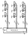
- FIG. 1 is an overall block diagram of a memory system according to an embodiment.
- FIG. 2 is a partial block diagram of the memory system of FIG. 1. It is a block diagram of the virtual SPD memory of the embodiment.
- FIG. 3 is a flowchart of a BIOS initialization process according to the embodiment. It is explanatory drawing of the content of the holding data and SPD data consistency check of the SPD memory of the memory module. It is explanatory drawing of the holding
- FIG. 7 is an explanatory diagram of an SDRAM capacity / bank address width conversion process of byte 4 in FIG. 6. It is explanatory drawing of the row / column address width of the byte 5 of FIG.
- FIG. 5 is a relationship diagram of DRAM capacity and SPD set value.
- FIG. 10 is a block diagram of a memory system according to a fifth embodiment. It is a block diagram of the memory system of 6th Embodiment. It is explanatory drawing of the conventional memory system. It is explanatory drawing of the other conventional memory system.
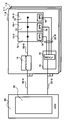
- FIG. 1 is an overall block diagram of a memory system according to an embodiment.
- FIG. 2 is a partial block diagram of the memory system of FIG.
- a CPU Central Processing Unit
- the memory controller 32 has a plurality of memory buses 20-0 to 20-2 and a plurality of serial buses 22-0 to 22-2. In this example, three memory buses 20-0 to 20-2 and three serial buses 22-0 to 22-2 are shown, but the number of buses is not limited thereto.
- the memory buses 20-0 to 20-2 are composed of a high-speed memory transmission system of DDR (Double Data Rate) 2 / DDR3 specifications.
- DDR Double Data Rate
- serial buses 22-0 to 22-2 a bus having a lower transmission speed than the memory bus is used.
- I2C Inter-Integrated Circuit
- This I2C communication bus can identify 3 bits, and one I2C communication bus can connect up to eight memory modules.
- the risers 1-0 to 1-2, 1-3 to 1-5, and 1-6 to 1-8 are connected to the memory buses 20-0 to 20-2 and the serial buses 22-0 to 22-2. Are connected to three memory slots.
- Each riser 1-0 to 1-8 includes a memory buffer chip 12 for memory expansion, a plurality of memory modules 10-0 to 10-3, and a memory interface circuit (referred to as a virtual SPD memory) 14. Yes.
- Each of the memory modules 10-0 to 10-3 has a nonvolatile memory 70 (also referred to as SPD in the figure) and a random access memory (RAM) on which memory specification information (SPD data: Serial Presence Detect Data) is mounted. 72.
- the virtual SPD memory 14 is connected to serial buses 22-0 to 22-2, and is connected to a nonvolatile memory (hereinafter referred to as an SPD memory) 70 of each memory module 10-0 to 10-3.
- the RAM 72 of each of the memory modules 10-0 to 10-3 is connected to the memory buses 20-0 to 20-2 via the buffer memory chip 12.
- FIG. 1 shows a system in which risers are mounted in all memory slots, but risers may be mounted in some of all memory slots, and the number of mounted risers can be changed according to the required memory capacity.
- the number of memory modules mounted on the riser is shown as four, a plurality of memory modules may be used.
- the configuration is as shown in FIG. That is, the risers 1-0 to 1-2 are connected to the memory controller 32 of the CPU 30 via the memory bus 20-0 and the serial bus 22-0.
- Each riser 1-0 to 1-2 is mounted with a memory buffer chip 12, a plurality of memory modules 10-0 to 10-2, and a virtual SPD memory 14.
- the memory buffer 12 is connected to the memory controller 32 and the RAM 72 of each of the memory modules 10-0 to 10-2 through the memory bus 20-0.
- the virtual SPD memory 14 is connected to the memory controller 32 and the SPD memory 70 of each of the memory modules 10-0 to 10-2 through the serial bus 22-0.
- the SPD memory 70 is a non-volatile memory in which memory specification information (SPD data: Serial Presence Detect Data) is mounted as will be described later.
- SPD data Serial Presence Detect Data
- 2 shows an example in which three memory modules 10-0 to 10-2 are mounted on the risers 1-0 to 1-2. However, as shown in FIG. 1, four memory modules 10-0 to 10-3 can be mounted on the risers 1-0 to 1-2.
- the virtual SPD memory 14 collects SPD data of the memory modules 10-0 to 10-3 in the riser, performs data consistency check, performs memory expansion conversion, and expands converted SPD data. Hold. In other words, the virtual SPD memory 14 holds SPD data obtained by converging SPD data of the SPD memories of the four memory modules 10-0 to 10-3 in the riser.
- the memory controller 32 can recognize that the plurality of memory modules of the riser are one memory module. That is, the number of memory modules can be expanded despite the limitation on the number of connections of the serial bus 22-0. Further, the memory controller 32 can omit the initialization process of the individual memory modules in the riser. For this reason, even if the number of memory modules is increased, the load on the BIOS can be reduced.
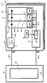
- FIG. 3 is a block diagram of the virtual SPD memory according to the embodiment.
- FIG. 4 is a flowchart of a BIOS initialization process according to the embodiment.
- FIG. 3 the same components as those shown in FIGS. 1 and 2 are denoted by the same symbols.
- the virtual SPD memory 14 includes a power supply voltage monitoring circuit 40, an SPD read sequencer 42, a local SPD bus (serial bus) 44, an SPD read register 46, an SPD data check unit 48, and an SPD.
- the data memory expansion conversion unit 50, the SPD write sequencer 52, the SPD command decode unit 54, and the SPD data storage unit 56 are included.
- the SPD read sequencer 42 reads the SPD data in the SPD memory 70 of the memory modules 10-0 to 10-3 to the SPD read register 46 via the local SPD bus 44 having the same configuration as the serial bus 22-0.
- the SPD data check unit 48 determines whether the SPD data of the memory modules 10-0 to 10-3 read into the SPD read register 46 matches.
- the SPD data memory expansion conversion unit 50 performs memory expansion conversion such as an address bit width from the SPD data of each of the memory modules 10-0 to 10-3 read to the SPD read register 46.
- the SPD write sequencer 52 writes the data of the SPD read register 46 to the SPD data storage unit 56 via the SPD command decode unit 54.
- the SPD command decode unit 54 is connected to the serial bus 22-0, receives the slave address from the memory controller 32, performs read access to the SPD data storage unit 56, and transfers the data in the SPD data storage unit 56 to the serial bus 22- Send to zero.
- the SPD read sequencer 42 includes an SPD read control unit 60 and an SPD bus control unit 62.
- the SPD read control unit 60 issues the local slave address LSA and the word address WA of the memory modules 10-0 to 10-3 to the SPD bus control unit 62 in response to the trigger signal Tr from the power supply voltage monitoring circuit 40.
- the SPD bus control unit 62 transmits the issued read command RD including the local slave address LSA and the word address WA to the SPD memory 70 of the memory modules 10-0 to 10-3 via the local SPD bus 44.
- the SPD write sequencer 52 includes an SPD write control unit 64 and an SPD bus control unit 66.
- the SPD write control unit 64 issues the SPD data storage unit 56 word address WA to the SPD bus control unit 62 in response to the trigger signal Tr from the SPD data memory expansion conversion unit 50.
- the SPD bus control unit 66 transmits a write command WD including the issued word address WA to the SPD command decoding unit 54.
- the power supply voltage monitoring circuit 40 operates to check the power supply voltage value.
- the power supply voltage monitoring circuit 40 outputs a trigger signal Tr to the SPD read sequencer when the power supply voltage value is a normal value within the standard.
- the SPD read sequencer 42 When the SPD read sequencer 42 receives the trigger signal Tr, the SPD read sequencer 42 starts collecting actual SPD data of the plurality of memory modules 10-0 to 10-3 under the memory buffer chip 12 (see FIGS. 1 and 2). That is, the SPD read controller 60 of the SPD read sequencer 42 generates a local SPD slave address LSA and an SPD word address WA.
- the local SPD slave address LSA is a signal for selecting the real SPD memory device 70 on the risers 1-0 (1-1 to 1-8).
- the SPD word address WA is a signal indicating the storage address of the selected SPD data in the real SPD memory device 70.
- the SPD bus control unit 62 receives the local SPD slave address LSA and the SPD word address WA from the SPD read control unit 60, generates an SPD read command RD, and transmits the command RD to the local SPD bus 44.
- the SPD data of the designated SPD memory device 70 is sequentially read and stored in the SPD read data register 46 via the local SPD bus 44.
- the read sequencer 42 repeats this process and collects all the SPD data in all the SPD memories 70 in the SPD read data register 46 (S20 in FIG. 4).
- the SPD data check unit 48 After the collected SPD data is temporarily stored in the SPD read data register 46, the SPD data check unit 48 performs data consistency check. The consistency check is to check whether the memory modules 10-0 to 10-3 under the buffer memory 12 satisfy the memory expansion requirement.
- coincidence determination it is checked whether the memory capacities are the same and whether the operation speeds are uniform.
- common timing calculation it is checked whether there is a variation in timing characteristics, and if there is, data processing is performed to absorb it (S22 and S24 in FIG. 4).
- match determination items are divided into two items: match required and match selection.
- Matching-required items are items that must be matched regardless of the memory expansion method.
- the coincidence selection item is an item that does not necessarily need to be coincident depending on the memory expansion method.
- the specifications of the memory modules 10-0 to 10-3 on the riser 1-0 are basically the same. However, depending on the expansion method of the memory buffer chip 12, there may be no problem even if the memory capacity and the operation speed do not match, so the matching items are classified into two.
- the match determination logic of the SPD data check unit 48 such that it is programmable by PLD (Programmable Logic Device) or has a plurality of modes. Thereby, it can respond flexibly to each expansion method.
- PLD Programmable Logic Device
- the common timing calculation item employs the maximum timing value between the memory modules. This is because the timing characteristic in the riser 1-0 is absorbed by adjusting the timing to the memory module having the slowest timing value.
- the SPD data check unit 48 displays the check error result.
- the error log Er is logged in the reserve bit of the SPD data storage unit 56 (S30 in FIG. 4).
- the BIOS can detect erroneous mounting of the memory module by looking at the log bits in the SPD data storage unit 56.
- the SPD data check unit 48 calculates the maximum value as the common timing
- the SPD data check unit 48 updates the corresponding field item in the SPD data storage unit 56 with the maximum value.
- the SPD data memory extension conversion unit 50 performs extension conversion of the SPD data (S26 in FIG. 4).
- the memory expansion conversion processing is SPD data processing such as expansion of the address bit width in order to increase the memory capacity to 2 times, 4 times, 8 times, or the like.
- the memory expansion conversion unit 50 preferentially expands the row address width of the memory module to the maximum value, and if that is not enough, expands the column address width.
- the memory expansion conversion unit 50 may be a hard wire fixed. However, it is desirable to implement such that the memory expansion conversion unit 50 is programmable by PLD or has a plurality of modes. Thereby, it can respond flexibly to each expansion method.
- the memory extension conversion unit 50 When the memory extension conversion unit 50 completes all the extension conversion processes, it rewrites the corresponding field in the SPD data storage unit 56 with the converted value. Then, the memory expansion conversion unit 50 outputs a trigger signal Tr to the SPD write sequencer 52. Upon receiving the trigger signal Tr, the SPD write sequencer 52 writes the updated SPD data (FIGS. 5 and 6) stored in the SPD read data register 46 to the SPD data storage unit 56.
- the SPD write control unit 64 of the SPD write sequencer 52 generates the SPD word address WA of the SPD data storage unit 56.
- the SPD bus control unit 66 receives the SPD word address WA from the SPD write control unit 64, generates an SPD write command WT, and transmits the write command to the SPD command decoding unit 54 (S28 in FIG. 4).
- the SPD command decode unit 54 decodes the SPD write command and writes the data designated by the word address of the SPD read register 46 in the SPD data storage unit 56.
- the SPD write sequencer 52 repeats this process to generate one virtual SPD memory (S30 in FIG. 4).
- the SPD data storage unit 56 has the same address map and data format as the actual SPD memory 70. Therefore, the BIOS can access the virtual SPD storage unit 56 via the serial bus 22-0 in the same manner as the real SPD memory 70. In other words, the memory can be expanded without changing the BIOS.
- step S14 If the boot process in step S12 is successful, the processor reset is released.
- the BIOS executed by the CPU 30 reads the SPD data in the SPD data storage unit 56 of the virtual SPD memory 14 of the riser 1-0 (1-1 to 1-8) via the serial bus 22-0. As described in steps S20 to S30 in FIG. 3 and FIG. 4, the virtual SPD memory 14 detects power-on, and the memory modules 10-0 to 10- of the risers 1-0 (1-1 to 1-8). 3 is executed, and the result is stored in the SPD data storage unit 56.
- the BIOS can perform the memory recognition processing of the SPD data of the memory modules 10-0 to 10-3 of the risers 1-0 (1-1 to 1-8) by one reading. For this reason, the burden of BIOS memory recognition processing can be reduced. That is, the BIOS initialization time can be shortened.
- the BIOS repeats this memory recognition process for the number of all the risers (and all memory modules) installed.
- the BIOS performs SPD data processing.
- the BIOS determines the operation speed, latency, access timing, and the like of the memory module of the riser based on the SPD data read from the virtual SPD memory 14 of each riser. In this case, since the determination of the access timing or the like in the riser has been completed, the BIOS only needs to determine the access timing or the like between the risers.
- BIOS initialization time can be shortened.
- BIOS performs the operation setting of the memory controller 32 and the initialization process of the RAM 72 mounted on the memory module based on the determined information.
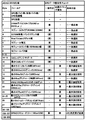
- FIG. 5 is an explanatory diagram of data held in the SPD memory 70 of the memory modules 10-0 to 10-3 and the contents of the SPD data consistency check.
- FIG. 5 is a relationship diagram showing the byte position and field contents of the SPD memory of the memory module of the DDR3 specification and the target of the SPD data consistency check. In FIG. 5, data that does not require a consistency check among the SPD data is omitted in the blank.
- SPD data is specification information that defines the type, capacity, maximum operating speed, support latency, timing characteristics, etc. of the memory module.
- FIG. 5 shows an example of SPD data of DDR3 specifications. In the DDR3 specification, SPD data has a field of 0 to 255 bytes.
- byte 0 specifies the total number of SPD bytes / number of valid bytes / CRC (Cyclic Redundancy Code) protection width.
- Byte 1 defines the SPD version number.
- the SPD data item to be determined for which the above-described matching is essential is indicated by “required” in FIG.
- the SPD data items to be determined to be coincident are the DRAM device type of byte 2, the module type of byte 3, the module voltage of byte 6, the module bus width of byte 8, and the CRC code of the SPD of bytes 126-127.
- Byte 2 DRAM (Dynamic Random Access Memory) device type specifies whether the memory module is DDR2 specification, DDR3 specification or other.
- the module type of byte 3 defines whether the memory module type is RDIMM (Registered Dual Inline Memory Module) or UDIMM (Unbaffered Dual Inline Memory Module).
- the module voltage of byte 6 defines the operating voltage value of the memory module.
- the module bus width of byte 8 defines the bus width of the memory module.
- the CRC code of the SPD in bytes 126 to 127 defines the CRC code value (CRC value of 0 to 116 bytes or CRC value of 0 to 125 bytes) of the SPD data.
- the aforementioned SPD data check unit 48 compares the SPD data items between the memory modules to determine whether they match. When the above-mentioned SPD data check unit 48 finds an item that does not match, it logs an error as an incorrect implementation as described above.
- the SPD data item of the determination item for which coincidence is selected is indicated by “(required)” in FIG. That is, the SPD data item of the determination item for which coincidence is selected includes the SDRAM capacity / bank address width of byte 4, the row / column address width of byte 5, and the module rank number of SDRAM 7 / SDRAM bit width. , Byte 12 SDRAM minimum cycle time, bytes 14-15 CAS (Column Address Strobe) latency support, byte 16 minimum CAS latency (tAA), byte 18 minimum RAS (Row Address Strobe) to CAS delay (tRCDmin), bytes 20 minimum precharge time (tRPmin).
- the items for which these matches are selected are selected when the characteristics of the buffer memory 12, the simultaneous read (Lockstep) operation or the duplex operation of a plurality of memory modules are performed.
- the paired memory modules must have the same specifications.
- the SPD data items used for the common timing calculation in the consistency check are indicated by “necessary” in the common timing calculation column of FIG. That is, the SPD data items used for the common timing calculation are the minimum write recovery time (tWRmin) of byte 17, the minimum RA (Row Address) to RA delay (tRRDmin) of byte 19, and tRAS / tRC (Bytes 22, 23) of byte 21.
- the timing characteristics have a certain amount of deviation due to semiconductor variations even between memory modules having the same speed specifications.
- the common timing calculation compares the timing characteristics of the individual memory modules and calculates a timing specification effective for all the memory modules.
- the SPD data check unit 48 selects the maximum value of the target SPD data and updates the corresponding field in the SPD data storage unit 56 to the selected value.
- FIG. 6 is an explanatory diagram of the data held in the SPD memory 70 of the memory modules 10-0 to 10-3 and the memory expansion conversion process.
- FIG. 6 shows the byte position and field contents of the SPD memory of the memory module of the DDR3 specification which is the same as FIG. In FIG. 6, as in FIG. 5, data that does not require consistency check and extended conversion in the SPD data is omitted in the blank.
- conversion items are indicated by "necessary" in the column of the conversion location. That is, the conversion location is the SDRAM capacity / bank address width of byte 4, the row / column address width of byte 5, the module rank number of byte 7 / SDRAM bit width, and the CRC code of the SPD of bytes 126-127.
- the latency countermeasure items are indicated by “necessary” in the latency countermeasure column of FIG.
- the latency countermeasure items are the minimum RA to RA delay time (tRRDmin) of byte 19 and the CRC code of the SPD of bytes 126 to 127.
- FIG. 7 is an explanatory diagram of the conversion process of the SDRAM capacity / bank address width of byte 4 in FIG.
- the SDRAM capacity / bank address width of byte 4 is composed of a 4-bit [3: 0] SDRAM capacity column and a 3-bit [6: 4] bank address width field. 3 adds the SDRAM capacity of the SPD data of each memory module, calculates the expanded capacity, and rewrites the SDRAM capacity column with the calculated capacity. The bank address width is not changed.
- FIG. 8 is an explanatory diagram of the row / column address width of byte 5 in FIG.
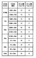
- FIG. 9 is a relationship diagram between the DRAM capacity and the SPD set value.
- FIG. 10 is a flowchart of the row / column address conversion process executed by the SPD data memory expansion unit 50.
- the row / column address width of byte 5 includes a 3-bit [2: 0] column address column and a 3-bit [5: 3] row address column.
- DRAM capacity shows six types of 512 Mbit, 1 Gbit, 2 Gbit, 4 Gbit, 8 Gbit, and 16 Gbit. Two DRAM configurations are defined for each DRAM capacity. Each DRAM configuration has two types of ⁇ 8 bits and ⁇ 4 bits.
- the row address (RA) bit width and column (CA) address bit width are set according to each DRAM capacity and DRAM configuration.
- the row address bit width is a maximum of 16 bits
- the column address bit width is a maximum of 12 bits.
- a DRAM having a capacity of 512 Mbit uses 13 bits for the row address bit width
- a DRAM having a capacity of 1 Gbit uses 14 bits for the row address bit width
- a DRAM with a capacity of 2 Gbit uses 15 bits for the row address bit width
- a DRAM with a capacity of 4 Gbit, 8 Gbit, 16 Gbit uses 16 bits for the row address bit width.
- a DRAM having a capacity of 512 Mbit, 1 Gbit, 2 Gbit, 4 Gbit and a configuration of 8 bits uses 10 bits for the column address bit width.
- a DRAM having a capacity of 512 Mbit, 1 Gbit, 2 Gbit, 4 Gbit and a configuration of ⁇ 4 bits uses 11 bits for the column address bit width.
- a DRAM having a capacity of 8 Gbit and a configuration of ⁇ 8 bits uses 11 bits for the column address bit width.
- a DRAM with a capacity of 8 Gbit and a configuration of ⁇ 4 bits and a DRAM with a capacity of 16 Gbit use 12 bits for the column address bit width.
- the SPD data memory expansion conversion unit 50 sets the number of virtual ranks.
- the virtual rank number is the virtual rank number of the riser and is usually smaller than the real rank number.
- the SPD data memory expansion conversion unit 50 adds the number of expansion bits to the row address (RA) width of the real SPD data in byte 5 in FIG.
- the SPD data memory expansion conversion unit 50 determines whether or not the calculated row address width is 16 bits or less which is the maximum value. When the SPD data memory expansion conversion unit 50 determines that the calculated row address width is equal to or less than the maximum value of 16 bits, it rewrites the corresponding field (see FIG. 8) of the SPD read register 46 with the calculated row address width. ,finish.
- the SPD data memory expansion conversion unit 50 determines that the calculated row address width is 17 bits, it expands the column address width. That is, the SPD data memory expansion conversion unit 50 adds 1 bit to the column address (CA) width of the actual SPD data of byte 5 in FIG. Then, the SPD data memory expansion conversion unit 50 sets the row address (RA) width to “16” which is the maximum value. That is, the extended portion by the column address (CA) is returned to the row address. The SPD data memory expansion conversion unit 50 rewrites the corresponding field (see FIG. 8) of the SPD read register 46 with the calculated row address width and column address width, and ends.
- FIG. 11 is an explanatory diagram of the conversion process of the number of module ranks of byte 7 / SDRAM bit width in FIG.
- the module rank number of byte 7 / SDRAM bit width is composed of a 3-bit [2: 0] SDRAM bit width column and a 3-bit [5: 3] rank number column.
- the SPD data memory expansion unit 50 in FIG. 3 sets the virtual rank number in the rank number column and rewrites it. Also, the SDRAM bit width is not changed.
- FIG. 12 is an explanatory diagram of the conversion process of the minimum RAS to RAS delay time (tRRDmin) of the byte 19 in FIG.
- the SPD data memory expansion conversion unit 50 in FIG. 3 adds the latency time of the buffer memory chip 12 (see FIGS. 1 and 2) to the field value.
- FIG. 13 is an explanatory diagram of the SPD CRC code recalculation process of bytes 126 to 127 in FIG.
- the CRC code of the SPD in bytes 126-127 has a 16-bit CRC value.
- the upper 8 bits are held in byte 127 and the lower 8 bits are held in byte 126.
- the CRC code value of the SPD data is a CRC value of 0 to 116 bytes or a CRC value of 0 to 125 bytes of the SPD data. One of them is designated by bit [7] of byte 0 in FIG.
- the SPD data conversion extension unit 50 recalculates the CRC from 0 to 125 bytes of the SPD data (after conversion and extension) in FIGS. , Write in the fields of bytes 126 and 127. Then, the SPD data conversion extension unit 50 rewrites the corresponding field (see FIGS. 5 and 6) of the SPD read register 46 with the calculated CRC value, and ends.
- the SPD read register unit 46 holds the SPD data having the field of 0 to 255 bytes shown in FIGS. 5 and 6, and the SPD data check unit 48 and the SPD data memory expansion conversion unit 50 detect coincidence. , Timing adjustment, rewritten to extended conversion value. Since the SPD data of the SPD read register unit 46 is written to the virtual SPD storage unit 56, the virtual SPD storage unit 56 reads the field of 0 to 255 bytes rewritten to the value subjected to coincidence detection, timing adjustment, and extended conversion. The SPD data possessed is stored.
- the BIOS can perform memory recognition processing of SPD data of the memory modules 10-0 to 10-3 of the risers 1-0 (1-1 to 1-8) by one reading. For this reason, the burden of BIOS memory recognition processing can be reduced. That is, the BIOS initialization time can be shortened.
- FIG. 14 is a block diagram of a memory system according to the second embodiment.
- the same components as those described in FIG. 2 are indicated by the same symbols.
- the memory controller 32 of the CPU 30 is connected to the bus switch 16 via the serial bus 22-0.
- the bus switch 16 is connected to the virtual SPD memory 14 described with reference to FIG. 3 and the SPD memories 70 of the memory modules 10-0 to 10-2 through the serial bus 22-0.
- the bus switch 16 is provided in the risers 1-0 to 1-2, and the bus switch 16 is switched by the address from the memory controller 32 to access the virtual SPD memory 14.
- the memory controller 32 can also access the SPD memory 70 of the memory modules 10-0 to 10-2.
- FIG. 15 is a block diagram of a memory system according to the third embodiment.
- the same components as those described in FIGS. 2 and 14 are indicated by the same symbols.
- the memory controller 32 of the CPU 30 is connected to the virtual SPD memory 14 via the serial bus 22-0.
- the virtual SPD memory 14 includes a bus switch 18.
- the bus switch 18 is connected to the SPD memory 70 of the memory modules 10-0 to 10-2 through the serial bus 22-0.
- a bus switch 18 is provided in the virtual SPD memory 14 of the risers 1-0 to 1-2, and the bus switch 18 is switched by an address from the memory controller 32, and also to the SPD memory 70 of the memory modules 10-0 to 10-2. Accessible.
- FIG. 16 is a block diagram of a memory system according to the fourth embodiment.
- a virtual SPD memory 14 is built in the buffer memory chip 12.
- the memory controller 32 of the CPU 30 is connected to the virtual SPD memory 14 in the buffer memory chip 12 via the serial bus 22-0.
- the virtual SPD memory 14 is connected to the SPD memory 70 of the memory modules 10-0 to 10-2 through the serial bus 22-0.
- the built-in virtual SPD memory 14 in the memory buffer chip 12 can reduce the LSI (Large Scaled Integrated) chip in the riser.
- FIG. 17 is a block diagram of a memory system according to the fifth embodiment.
- the memory controller 32 of the CPU 30 is connected to the virtual SPD memory 14 via the serial bus 22-0.
- the virtual SPD memory 14 is connected to the SPD memory 70 of the memory modules 10-0 to 10-2 through the serial bus 22-0.
- This virtual SPD memory 14 includes a ROM (Read Only Memory) 24 that stores SPD data check logic data and SPD data expansion conversion logic data, and a PLD (Programmable) that can change the check logic and expansion conversion logic in a programmable manner using the logic data in the ROM 24.
- ROM Read Only Memory
- PLD Programmable
- Logic Device 26.
- the circuits of the SPD data check unit 48 and the SPD data extension conversion unit 50 described in FIG. 2 can be changed in a programmable manner. That is, it becomes possible to flexibly cope with the SPD specification change.
- FIG. 18 is a block diagram of a memory system according to the sixth embodiment.
- the same components as those described in FIG. 2 are denoted by the same symbols.
- the memory controller 32 of the CPU 30 is connected to the virtual SPD memory 14A via the serial bus 22-0.
- the virtual SPD memory 14A is connected to the SPD memory 70 of the memory modules 10-0 to 10-2 through the serial bus 22-0.
- the virtual SPD memory 14A has the SPD data check (coincidence detection) function described in FIG. 5, and does not have the SPD data common timing function and the SPD data extension conversion function.
- the error log of the data check in the virtual SPD memory 14A is logged in a free area in the storage unit of the virtual SPD memory 14A. Then, the BIOS accesses the real SPD memory 70 of the memory modules 10-0 to 10-2 as usual and performs memory initialization processing.
- the virtual SPD memory 14A can be mounted on the riser 1-0 of another manufacturer without being changed. Also, since the virtual SPD memory executes the BIOS SPD data check instead, the load on the BIOS can be reduced.
- the memory circuit is described as DIMM, but a memory module circuit having another configuration can be applied.
- the memory bus has been described in the example of DDR3 of the time division address and command transmission method, but it can be applied to other time division address and command transmission methods such as DDR and DDR2.
- the I2C bus has been described as the control bus, other types of control buses can be used.
- the specification information of multiple memory circuits is collected, common specification information is created, and the memory interface circuit to be stored is connected to the control bus of the processing unit, the number of memory connections of the memory bus can be increased. Even if the memory is increased on the memory bus, the initialization process of the processing unit can be shortened.
Landscapes
- Engineering & Computer Science (AREA)
- Theoretical Computer Science (AREA)
- Physics & Mathematics (AREA)
- General Engineering & Computer Science (AREA)
- General Physics & Mathematics (AREA)
- Techniques For Improving Reliability Of Storages (AREA)
Abstract
処理ユニット(30)がメモリバス(20-0)を介し複数のメモリ回路(10-0~10-3)のデータの入出力を行うメモリシステムにおいて、複数のメモリ回路(10-0~10-3)の仕様情報を収集し、共通の仕様情報を作成し、格納するメモリインターフェース回路(14)を処理ユニットの制御バスに接続した。このため、メモリバスのメモリ接続数を増加できる。又、メモリバスにメモリを増加しても、処理ユニットの初期化処理を短縮できる。
Description
本発明は、メモリシステム、メモリ装置及びメモリインターフェース装置に関する。
高速で大容量なメモリシステムは、情報処理装置の高速化及び処理能力の向上に有効である。例えば、サーバーシステムの仮想化の急速な普及に伴って、既存システムのメモリの搭載容量が不足している。
図19は、従来のメモリシステムの構成図である。CPU(Central Processing Unit)100はメモリコントローラ102を有する。メモリコントローラ102は、3つのメモリバス112-0~112-2を有する。3枚のメモリモジュール110-0~110-2,110-3~110-5,110-6~110-8が、各メモリバス112-0~112-2にスロットを介し接続される。DDR(Double Data Rate)2/DDR3のような高速メモリ伝送システムでは、1つのメモリバスは2~3枚のメモリモジュールをメモリスロットに接続するのが限界である。
又、メモリコントローラ102が各メモリモジュール110-0~110-2,110-3~110-5,110-6~110-8の状態把握及び状態設定等の行うため、メモリコントローラ102は3つのシリアルバス114-0~114-2を介し、3枚のメモリモジュール110-1~110-2,110-3~110-5,110-6~110-8に接続する。このシリアルバス114-0~114-2は、メモリバスに比較し、伝送速度の遅いバスが使用される。例えば、I2C(Inter-Integrated Circuit)通信バスを利用する。このI2C通信バスは3ビットの識別が可能であり、1つのI2C通信バスはメモリモジュールを最大8個まで接続できる。
図20は、他の従来のメモリシステムの構成図である。図20において、メモリバス112-0~112-2、シリアルバス114-0~114-2、メモリスロットの数は、図19の従来システムと同じである。図20では、メモリの拡張のため、この既存システムのメモリスロットに、ライザー120-0~120-2を接続する。
ライザー120-0~120-2には、メモリ拡張用のメモリバッファチップ122と複数のメモリモジュール124-0~124-3とが搭載されている。この例では、1つのメモリスロットがライザー120-0~120-2によって、4つのメモリスロットに拡張される。各メモリモジュール124-0~124-3のSPDメモリはシリアルバス114-0~114-2に直接接続される。又、各メモリモジュール124-0~124-3のRAMは、バッファメモリチップ122を介しメモリバス112-0~112-2に接続される。すなわちメモリ容量を4倍に拡張することが可能である。
一方、コンピュータシステムに電源が投入されると、ブート処理と呼ばれるオペレーティングシステム(OS:Operating System)の立ち上げ処理を開始する。この立ち上げ処理には、BIOS(Basic Input Output System)等のファームウェアやOSによる各種ハードウェアの初期化と診断、コンピュータシステムへの各種ハードウェアの組込み処理等が含まれる。
メモリの初期化処理はシリアルバス114-0~114-2を介しBIOSが行う。この初期化処理においては、BIOSは、メモリモジュールに搭載される不揮発性メモリ(以下、SPD(Serial Presence Detect)メモリと称す)に格納されているメモリモジュールの仕様情報(以下、SPDデータ)と言う)を読み出し、BIOSが、メモリモジュールの動作スピード、レイテンシ、アクセスタイミング等を決定する。更に、BIOSは、この決定した情報をもとにメモリコントローラの動作設定及びメモリモジュールに搭載されたRAM(Random Access Memory)の初期化処理を行う。
このようなメモリシステムでは、メモリの増加とともに、BIOSのメモリ初期化処理の負担が重くなり、メモリモジュール誤実装によるシステム障害が発生するおそれがある。BIOSのメモリ初期化処理の負担を軽減するため、BIOSに代わって、SPDデータの収集を行い、メモリ搭載ミスをチェックするメモリ初期化制御装置を、メモリモジュールと別に設けることが提案されている。
図20に示したように、ライザー120-0~120-2のメモリモジュール124-0~124-3のSPDメモリがシリアルバス114-0~114-2に直接接続するので、SPDメモリのバス接続数がボトルネックとなって、ライザーの追加数が制限されてしまう。例えば、前述のI2C通信バスをシリアスバスに使用する場合は、メモリモジュールのSPDメモリのバス最大接続数は、1つのシリアルバスあたり8個である。
図20においては、1つのシリアルバス毎のSPDメモリの接続数は6個であり、最大接続数の8個以下なので問題はない。しかし、1つのシリアルバスにライザー120-0を2個追加すると、最大接続数を越えてしまうので、ライザーを更に追加することはできない。このため、メモリの拡張に制限が生じる。
本発明の目的は、複数のメモリモジュールを搭載したメモリ装置の搭載数を増加するメモリシステム、メモリ装置及びメモリインターフェース装置を提供することにある。
この目的の達成のため、開示のメモリシステムは、揮発性メモリと前記揮発性メモリのデータ入出力の仕様情報を格納する不揮発性メモリとを有する複数のメモリ回路と、前記複数のメモリ回路の前記不揮発性メモリに制御バスで接続されたメモリインターフェース回路とを有するメモリ装置と、メモリバスを介し前記揮発性メモリのデータ入出力制御を行うメモリコントローラを有する処理ユニットとを有し、前記メモリインターフェース回路は、前記制御バスを介し前記複数のメモリ回路の前記不揮発性メモリの前記仕様情報を読み出し、読み出した前記複数のメモリ回路の前記仕様情報から、少なくとも前記複数のメモリ回路がメモリ拡張要件を満たすか否かの判定を行う処理回路と、前記処理ユニットと制御バスで接続され、前記処理回路の判定結果を格納する記憶部とを有し、前記処理ユニットは、前記制御バスを介し前記記憶部の格納情報を読み出し、前記メモリコントローラを初期化処理する。
又、この目的の達成のため、開示のメモリ装置は、揮発性メモリと前記揮発性メモリのデータ入出力の仕様情報を格納する不揮発性メモリとを有する複数のメモリ回路と、メモリバスを介し前記揮発性メモリのデータ入出力制御を行う処理ユニットと制御バスで接続され、前記複数のメモリ回路の前記不揮発性メモリに制御バスで接続されたメモリインターフェース回路とを有し、前記メモリインターフェース回路は、前記制御バスを介し前記複数のメモリ回路の前記不揮発性メモリの前記仕様情報を読み出し、読み出した前記複数のメモリ回路の前記仕様情報から、少なくとも前記複数のメモリ回路がメモリ拡張要件を満たすか否かの判定を行う処理回路と、前記制御バスに接続され、前記処理ユニットの初期化処理のための前記処理回路の判定結果を格納する記憶部とを有する。
更に、この目的の達成のため、開示のメモリインターフェース回路は、揮発性メモリと前記揮発性メモリのデータ入出力の仕様情報を格納する不揮発性メモリとを有する複数のメモリ回路の前記不揮発性メモリに制御バスで接続され、且つメモリバスを介し前記揮発性メモリのデータ入出力制御を行う処理ユニットと制御バスで接続されたメモリインターフェース回路であって、前記メモリインターフェース回路は、前記制御バスを介し前記複数のメモリ回路の前記不揮発性メモリの前記仕様情報を読み出し、読み出した前記複数のメモリ回路の前記仕様情報から、少なくとも前記複数のメモリ回路がメモリ拡張要件を満たすか否かの判定を行う処理回路と、前記制御バスに接続され、前記処理ユニットの初期化処理のための前記処理回路の判定結果を格納する記憶部とを有する。
複数のメモリ回路の仕様情報を収集し、共通の仕様情報を作成し、格納するメモリインターフェース回路を処理ユニットの制御バスに接続したので、メモリバスのメモリ接続数を増加できる。又、メモリバスにメモリを増加しても、処理ユニットの初期化処理を短縮できる。
以下、実施の形態の例を、メモリシステムの第1の実施の形態、仮想SPDメモリ、メモリの一致/拡張変換処理、メモリシステムの他の実施の形態の順で説明するが、開示のメモリシステム、メモリ装置、メモリインターフェース装置は、この実施の形態に限られない。
(メモリシステムの第1の実施の形態)
図1は、実施の形態のメモリシステムの全体ブロック図である。図2は、図1のメモリシステムの部分ブロック図である。図1に示すように、CPU(Central Processing Unit)30は演算処理ユニット(図示せず)とメモリコントローラ32とを有する。メモリコントローラ32は、複数のメモリバス20-0~20-2と複数のシリアルバス22-0~22-2とを有する。この例では、3つのメモリバス20-0~20-2と3つのシリアルバス22-0~22-2を示すが、このバス数に限られない。
図1は、実施の形態のメモリシステムの全体ブロック図である。図2は、図1のメモリシステムの部分ブロック図である。図1に示すように、CPU(Central Processing Unit)30は演算処理ユニット(図示せず)とメモリコントローラ32とを有する。メモリコントローラ32は、複数のメモリバス20-0~20-2と複数のシリアルバス22-0~22-2とを有する。この例では、3つのメモリバス20-0~20-2と3つのシリアルバス22-0~22-2を示すが、このバス数に限られない。
又、メモリバス20-0~20-2は、DDR(Double Data Rate)2/DDR3仕様の高速メモリ伝送システムで構成される。シリアルバス22-0~22-2は、メモリバスに比較し、伝送速度の遅いバスが使用される。例えば、I2C(Inter-Integrated Circuit)通信バスを利用する。このI2C通信バスは3ビットの識別が可能であり、1つのI2C通信バスはメモリモジュールを最大8個まで接続できる。
ライザー1-0~1-2,1-3~1-5,1-6~1-8は、各メモリバス20-0~20-2と各シリアルバス22-0~22-2に接続された3つのメモリスロットにそれぞれ接続される。
各ライザー1-0~1-8には、メモリ拡張用のメモリバッファチップ12と複数のメモリモジュール10-0~10-3と、メモリインターフェース回路(仮想SPDメモリと称す)14とが搭載されている。各メモリモジュール10-0~10-3はメモリの仕様情報(SPDデータ:Serial Presence Detect Data)を搭載する不揮発性メモリ70(図では、SPDとも記す)とランダムアクセスメモリ(RAM:Random Access Memory)72とを有する。
図1の例では、ライザー1-0~1-8が、4つのメモリモジュール10-0~10-3を搭載するため、1つのメモリスロットがライザー1―0~1-8によって、4つのメモリスロットに拡張される。仮想SPDメモリ14はシリアルバス22-0~22-2に接続し、且つ各メモリモジュール10-0~10-3の不揮発性メモリ(以下、SPDメモリという)70に接続する。又、各メモリモジュール10-0~10-3のRAM72は、バッファメモリチップ12を介しメモリバス20-0~20-2に接続される。
図1の例は、全メモリスロットにライザーを搭載したシステムを示すが、全メモリスロットの一部にライザーを搭載しても良く、必要なメモリ容量に応じて、ライザー搭載数を変更できる。又、ライザーが搭載するメモリモジュール数を4個で示しているが、複数であれば良い。
図1のメモリシステム全体を、1つのメモリバス20-0、1つのシリアルバス22-0を対象にすると、図2に示す構成となる。即ち、ライザー1-0~1-2がメモリバス20-0、シリアルバス22-0を介しCPU30のメモリコントローラ32に接続する。各ライザー1-0~1-2は、メモリバッファチップ12と、複数のメモリモジュール10-0~10-2と、仮想SPDメモリ14とが搭載される。メモリバッファ12はメモリバス20-0によりメモリコントローラ32と各メモリモジュール10-0~10-2のRAM72とに接続する。
仮想SPDメモリ14は、シリアルバス22-0によりメモリコントローラ32と各メモリモジュール10-0~10-2のSPDメモリ70とに接続する。SPDメモリ70は後述するようにメモリの仕様情報(SPDデータ:Serial Presence Detect Data)を搭載する不揮発性メモリである。尚、図2では、ライザー1-0~1-2に3つのメモリモジュール10-0~10-2を搭載する例で図示する。しかし、図1に示したように、ライザー1-0~1-2に4つのメモリモジュール10-0~10-3を搭載することもできる。
後述するように、仮想SPDメモリ14は、ライザー内のメモリモジュール10-0~10-3のSPDデータを収集し、データの整合性チェックを行い、且つメモリ拡張変換を行い、拡張変換したSPDデータを保持する。即ち、仮想SPDメモリ14は、ライザー内の4つのメモリモジュール10-0~10-3のSPDメモリのSPDデータを収約したSPDデータを保持する。
このため、メモリコントローラ32は、ライザーの複数のメモリモジュールがあたかも1つのメモリモジュールであると認識できる。即ち、シリアルバス22-0の接続数の制限にもかかわらず、メモリモジュール数を拡張できる。又、メモリコントローラ32は、ライザー内の個々のメモリモジュールの初期化処理を省略できる。このため、メモリモジュール数を増加しても、BIOSの負荷を軽減することができる。
(仮想SPDメモリ)
図3は、実施の形態の仮想SPDメモリのブロック図である。図4は、実施の形態のBIOSの初期化処理フロー図である。図3において、図1及び図2で示したものと同一のものは、同一の記号で示してある。
図3は、実施の形態の仮想SPDメモリのブロック図である。図4は、実施の形態のBIOSの初期化処理フロー図である。図3において、図1及び図2で示したものと同一のものは、同一の記号で示してある。
図3に示すように、仮想SPDメモリ14は、電源電圧監視回路40と、SPD読出しシーケンサ42と、ローカルSPDバス(シリアルバス)44と、SPD読出しレジスタ46と、SPDデータチェック部48と、SPDデータメモリ拡張変換部50と、SPD書き込みシーケンサ52と、SPDコマンドデコード部54と、SPDデータ記憶部56とを有する。
SPD読出しシーケンサ42は、シリアルバス22-0と同じ構成のローカルSPDバス44を介しメモリモジュール10-0~10-3のSPDメモリ70のSPDデータを、SPD読出しレジスタ46に読み出す。SPDデータチェック部48は、SPD読出しレジスタ46に読みだされた各メモリモジュール10-0~10-3のSPDデータの一致判定を行う。
SPDデータメモリ拡張変換部50は、SPD読出しレジスタ46に読みだされた各メモリモジュール10-0~10-3のSPDデータからアドレスビット幅等のメモリ拡張変換を行う。SPD書き込みシーケンサ52は、SPDコマンドデコード部54を介しSPDデータ記憶部56にSPD読み出しレジスタ46のデータを書き込む。又、SPDコマンドデコード部54は、シリアルバス22-0と接続し、メモリコントローラ32からスレーブアドレスを受けと、SPDデータ記憶部56をリードアクセスし、SPDデータ記憶部56のデータをシリアルバス22-0に送出する。
又、SPD読み出しシーケンサ42は、SPD読み出し制御部60と、SPDバス制御部62とを有する。SPD読み出し制御部60は、電源電圧監視回路40からのトリガー信号Trに応じて、メモリモジュール10-0~10-3のローカルスレーブアドレスLSAとワードアドレスWAをSPDバス制御部62に発行する。SPDバス制御部62は、発行されたローカルスレーブアドレスLSAとワードアドレスWAを含むリードコマンドRDをローカルSPDバス44を介しメモリモジュール10-0~10-3のSPDメモリ70に送信する。
SPD書き込みシーケンサ52は、SPD書き込み制御部64とSPDバス制御部66とを有する。SPD書き込み制御部64は、SPDデータメモリ拡張変換部50からのトリガー信号Trに応じて、SPDデータ記憶部56ワードアドレスWAをSPDバス制御部62に発行する。SPDバス制御部66は、発行されたワードアドレスWAを含むライトコマンドWDをSPDコマンドデコード部54に送信する。
次に、図4を参照して、図3の仮想SPDメモリ14の動作を説明する。システムの電源が入力されると、電源電圧監視回路40が動作して、電源電圧値をチェックする。電源電圧監視回路40は、電源電圧値が規格内の正常な値であるとき、電源電圧監視回路40はSPD読出しシーケンサにトリガー信号Trを出力する。
SPD読出しシーケンサ42は、トリガー信号Trを受けると、メモリバッファチップ12(図1、図2参照)の配下にある複数のメモリモジュール10-0~10-3の実SPDデータの収集を開始する。即ち、SPD読出しシーケンサ42のSPD読出し制御部60は、ローカルSPDスレーブアドレスLSAとSPDワードアドレスWAを生成する。ローカルSPDスレーブアドレスLSAは、ライザー1-0(1-1~1-8)上の実SPDメモリデバイス70を選択する信号である。SPDワードアドレスWAは、選択し実SPDメモリデバイス70のSPDデータの格納番地を示す信号である。
SPDバス制御部62は、SPD読出し制御部60からローカルSPDスレーブアドレスLSAとSPDワードアドレスWAとを受け取り、SPDリードコマンドRDを生成し、そのコマンドRDをローカルSPDバス44に送信する。指定されたSPDメモリデバイス70のSPDデータが順次読みだされ、ローカルSPDバス44を介しSPD読み出しデータレジスタ46に格納される。読出しシーケンサ42はこの処理を繰り返し行い、全SPDメモリ70の全SPDデータをSPD読み出しデータレジスタ46に収集する(図4のS20)。
収集したSPDデータがSPD読出しデータレジスタ46に一旦格納された後、SPDデータチェック部48がデータの整合性チェックを行う。整合性チェックは、バッファメモリ12の配下のメモリモジュール10-0~10-3がメモリ拡張要件を満たすかどうかチェックするものである。
整合性チェックは、一致判定と共通タイミング算出の2つがある。一致判定は、メモリ容量が同一であるか、動作スピードは揃っているか等のチェックを行う。共通タイミング算出は、タイミング特性のバラつきがないかチェックを行い、ある場合はそれを吸収するデータ処理を行う(図4のS22、S24)。
図5で後述するように、一致判定の項目は、一致必須と一致選択の2つの項目に分けられる。一致必須項目は、メモリ拡張方式に関係なく、一致が必須である項目のことである。又、一致選択項目は、メモリ拡張方式によっては必ずしも一致している必要がない項目のことである。ライザー1-0上の各メモリモジュール10-0~10-3の仕様は全て同一であることが基本である。しかし、メモリバッファチップ12の拡張方式によっては、メモリ容量や動作スピード等は不一致でも問題ない場合があるため、一致項目を2つに分類している。
そのため、SPDデータチェック部48の一致判定のロジックは、PLD(Programable Logic Device)でプログラマブルにする、又は複数モードを持たせる、といった実装を行うことが望ましい。これにより、各拡張方式に柔軟に対応できる。
又、図5で説明するように、共通タイミング算出の項目は、各メモリモジュール10-0~10-3のタイミング特性にバラつきがある場合、各メモリモジュール間のタイミング値の最大値を採用する。この理由は、一番タイミング値が遅いメモリモジュールにタイミングを合わせることによって、ライザー1-0内のタイミング特性のバラつきを吸収するためである。
SPDデータチェック部48は、SPDデータの一致判定により整合性チェックに問題がある場合、すなわち、メモリ拡張要件を満たさないメモリモジュールが誤ってライザー1-0に実装された場合は、チェックエラー結果をSPDデータ記憶部56のリザーブビットにエラーログErとしてログする(図4のS30)。BIOSはSPDデータ記憶部56のログビットを見ることによって、メモリモジュールの誤実装を検出できる。
一方、SPDデータチェック部48は、最大値を共通タイミングとして算出した場合には、SPDデータ記憶部56の該当フィールド項目を、最大値で更新する。
SPDデータチェック部46が、SPDデータの一致判定により整合性に問題がないと判断する場合、SPDデータメモリ拡張変換部50がSPDデータを拡張変換する(図4のS26)。メモリ拡張変換処理は、メモリ容量を2倍、4倍、8倍、、、に増やすために、アドレスビット幅を拡張する等のSPDデータ処理である。
図6以下において後述するように、メモリ拡張変換部50は、メモリモジュールのローアドレス幅を優先的に最大値まで拡張し、それでも足りない場合は、カラムアドレス幅を拡張する。このメモリ拡張変換部50は、ハードワイヤ固定でも良い。しかしながら、メモリ拡張変換部50を、PLDでプログラマブルにする、又は複数モードを持たせる、といった実装を行うことが望ましい。これにより、各拡張方式に柔軟に対応できる。
メモリ拡張変換部50は全ての拡張変換処理を終了すると、SPDデータ記憶部56の該当フィールドを変換した値に書き換える。そして、メモリ拡張変換部50はSPD書込みシーケンサ52にトリガー信号Trを出力する。SPD書込みシーケンサ52は、トリガー信号Trを受けると、SPD読出しデータレジスタ46に格納された更新されたSPDデータ(図5、図6)をSPDデータ記憶部56に書き込む。
SPD書込みシーケンサ52のSPD書込み制御部64は、SPDデータ記憶部56のSPDワードアドレスWAを生成する。SPDバス制御部66は、SPD書込み制御部64からSPDワードアドレスWAを受け取り、SPDライトコマンドWTを生成し、ライトコマンドをSPDコマンドデコード部54に送信する(図4のS28)。
SPDコマンドデコード部54は、SPDライトコマンドをデコードして、SPDデータ記憶部56にSPD読み出しレジスタ46のワードアドレスで指定されたデータを書き込む。SPD書込みシーケンサ52はこの処理を繰り返し行い、1つの仮想SPDメモリを生成する(図4のS30)。
SPDデータ記憶部56は、実SPDメモリ70と同一のアドレスマップやデータフォーマットを備える。したがって、BIOSは、実SPDメモリ70と同じようにシリアルバス22-0を介し、仮想SPD記憶部56にアクセスできる。すなわち、BIOSの変更をすることなく、メモリ拡張が可能である。
次に、図4によりBIOS及び仮想SPDメモリの処理を説明する。
(S10)電源の投入により、CPU30のOSの立ち上げ処理のためのブート処理が起動する。又、前述した仮想SPDメモリ14の仮想SPDメモリ作成処理が起動する。
(S12)CPU30のブート処理では、CPU30及びメモリシステムを含む周辺回路のチップセットの設定を行う。次に、ブート処理は、バスの調整を行う。その後、ブート処理は、CPU30のプロセッサの内部設定を行う。
(S14)ステップS12のブート処理が成功した場合、プロセッサのリセットが解除される。
(S16)プロセッサのリセットが解除されると、プロセッサはBIOSを起動する。
(S32)CPU30の実行するBIOSは、シリアルバス22-0を介しライザー1-0(1-1~1-8)の仮想SPDメモリ14のSPDデータ記憶部56のSPDデータを読み出す。図3、図4のステップS20~S30で説明したように、仮想SPDメモリ14は、電源投入を検出し、ライザー1-0(1-1~1-8)のメモリモジュール10-0~10-3の初期化処理を実行し、その結果をSPDデータ記憶部56に格納している。
従って、BIOSは、1回の読み出しにより、ライザー1-0(1-1~1-8)のメモリモジュール10-0~10-3のSPDデータのメモリ認識処理が可能となる。このため、BIOSのメモリ認識処理の負担を軽減できる。即ち、BIOSの初期化時間を短縮できる。当然、メモリスロットにライザー構成でないメモリモジュール(図19、図20)を混在して搭載した場合には、ライザー以外のこれらのメモリモジュールのSPDデータを読み出す。BIOSは、このメモリ認識処理を、搭載された全ライザー(及び全メモリモジュール)枚数分だけ繰り返し行う。
(S34)次に、BIOSはSPDデータ処理を行う。BIOSは、各ライザーの仮想SPDメモリ14から読み出したSPDデータをもとに、ライザーのメモリモジュールの動作スピード、レイテンシ、アクセスタイミング等を決定する。この場合、ライザー内のアクセスタイミング等の決定は終了しているため、BIOSは、ライザー間のアクセスタイミング等を決定するだけで良い。
従って、BIOSはSPDデータ拡張変換を行う必要がなく、BIOSのSPDデータ処理の負担を軽減できる。即ち、BIOSの初期化時間を短縮できる。
(S36)BIOSは、この決定した情報をもとに、メモリコントローラ32の動作設定及びメモリモジュールに搭載されたRAM72の初期化処理を行う。
(メモリの一致/拡張変換処理)
次に、前述したメモリの一致及び拡張変換処理を説明する。図5は、メモリモジュール10-0~10-3のSPDメモリ70の保持データとSPDデータ整合性チェックの内容の説明図である。図5は、DDR3仕様のメモリモジュールのSPDメモリのバイト位置及びフィールド内容と、SPDデータ整合チェックの対象を示す関係図である。尚、図5において、SPDデータの内、整合性チェックを要しないデータは空欄で省略してある。
次に、前述したメモリの一致及び拡張変換処理を説明する。図5は、メモリモジュール10-0~10-3のSPDメモリ70の保持データとSPDデータ整合性チェックの内容の説明図である。図5は、DDR3仕様のメモリモジュールのSPDメモリのバイト位置及びフィールド内容と、SPDデータ整合チェックの対象を示す関係図である。尚、図5において、SPDデータの内、整合性チェックを要しないデータは空欄で省略してある。
図5に示すように、SPDデータは、メモリモジュールの種類、容量、最高動作スピード、サポートレイテンシ、タイミング特性等を規定した仕様情報である。図5では、DDR3仕様のSPDデータを例に示す。DDR3仕様では、SPDデータは、0~255バイトのフィールドを持つ。
例えば、バイト0は、SPD総バイト数/有効バイト数/CRC(Cyclic Redundancy Code)保護幅を規定する。又、バイト1は、SPDの版数を規定する。前述の一致が必須である判定対象のSPDデータ項目は、図5の「要」で示してある。
即ち、一致必須判定対象のSPDデータ項目は、バイト2のDRAMデバイスタイプ、バイト3のモジュールタイプ、バイト6のモジュール電圧、バイト8のモジュールバス幅、バイト126-127のSPDのCRCコードである。
バイト2のDRAM(Dynamic Random Access Memory)デバイスタイプは、メモリモジュールがDDR2仕様かDDR3仕様かそれ以外かを規定する。バイト3のモジュールタイプは、メモリモジュールの種類がRDIMM(Registered Dual Inline Memory Module)か、UDIMM(Unbaffered Dual Inline Memory Module)かを規定する。バイト6のモジュール電圧は、メモリモジュールの動作電圧値を規定する。バイト8のモジュールバス幅は、メモリモジュールのバス幅を規定する。バイト126-127のSPDのCRCコードは、SPDデータのCRCコード値(0~116ByteのCRC値又は0~125ByteのCRC値)を規定する。
これらのSPDデータは、各メモリモジュールで一致しないと、動作不能となる。前述のSPDデータチェック部48は、各メモリモジュール間でこのSPDデータ項目が一致するか否かを比較し、一致判定を行う。前述のSPDデータチェック部48は、一致しない項目が見つかると、前述のように誤実装として、エラーログする。
又、一致が選択される判定項目のSPDデータ項目は、図5の「(要)」で示す。即ち、一致が選択される判定項目のSPDデータ項目は、バイト4のSDRAM容量/バンクアドレス幅、バイト5のロー(Raw)/カラム(Column)アドレス幅、バイト7のモジュールランク数/SDRAMビット幅、バイト12のSDRAM最小サイクルタイム、バイト14-15のCAS(Column Address Strobe)レイテンシサポート、バイト16の最小CASレイテンシ(tAA)、バイト18の最小RAS(Row Address Strobe)toCASデレイ(tRCDmin)、バイト20の最小プリチャージ時間(tRPmin)である。
これらの一致が選択される項目は、バッファメモリ12の特性や複数メモリモジュールの同時リード(Lockstepという)動作や二重化動作を行う場合に選択される。例えば、ペアとなるメモリモジュールは同一仕様でなければならないからである。
一方、整合性チェックにおける共通タイミング計算に用いられるSPDデータの項目は、図5の共通タイミング算出欄の「要」で示す。即ち、共通タイミング計算に用いられるSPDデータの項目は、バイト17の最小ライトリカバリ時間(tWRmin)、バイト19の最小RA(Row Address)toRAデレイ(tRRDmin)、バイト21のtRAS/tRC(Byte22,23)の上位ビット、バイト22の最小ACT(Bank Active)toプリチャージデレイ(tRAmin)、バイト23の最小ACTtoACTデレイ(tRCmin)、バイト24-25の最小リフレッシュリカバリ時間(tRFC)、バイト26の最小ライトtoリードデレイ時間(tWTRmin)、バイト27の最小リードtoプリチャージデレイ(tRTPmin)、バイト126-127のSPDのCRCコードである。
これらのメモリモジュールのタイミングや速度に関する仕様では、同一速度の仕様のメモリモジュール間でも、半導体のバラツキによりタイミング特性がある程度ズレ幅を持っている。このズレ幅に対処するため、共通タイミング計算は、個々メモリモジュールのタイミング特性を比較し、全メモリモジュールに有効なタイミング仕様を計算する。この例では、図5の処理内容に記載されたように、SPDデータチェック部48は、対象SPDデータの最大値を選択し、SPDデータ記憶部56の該当フィールドを選択値に更新する。
図6は、メモリモジュール10-0~10-3のSPDメモリ70の保持データとメモリ拡張変換処理の説明図である。図6は、図5と同一であるDDR3仕様のメモリモジュールのSPDメモリのバイト位置及びフィールド内容を示し、且つフィールド内容に対しメモリ拡張変換の変更個所、レイテンシ対策項目、処理内容を示す。尚、図6において、図5と同様に、SPDデータの内、整合性チェックと拡張変換を要しないデータは空欄で省略してある。
図6において、変換項目は、変換個所の欄に「要」で示す。即ち、変換個所は、バイト4のSDRAM容量/バンクアドレス幅、バイト5のロー/カラムアドレス幅、バイト7のモジュールランク数/SDRAMビット幅、バイト126-127のSPDのCRCコードである。
同様に、レイテンシ対策項目は、図6のレイテンシ対策欄の「要」で示す。レイテンシ対策項目は、バイト19の最小RAtoRAデレイ時間(tRRDmin)、バイト126-127のSPDのCRCコードである。
図7は、図6のバイト4のSDRAM容量/バンクアドレス幅の変換処理の説明図である。バイト4のSDRAM容量/バンクアドレス幅は、4ビット[3:0]のSDRAM容量欄と3ビット[6:4]のバンクアドレス幅欄とで構成される。図3のSPDデータメモリ拡張部50は、各メモリモジュールのSPDデータのSDRAM容量を加算し、拡張した容量を計算し、計算した容量でSDRAM容量欄を書き換える。又、バンクアドレス幅は変更しない。
図8は、図6のバイト5のロー/カラムアドレス幅の説明図である。図9はDRAM容量とSPD設定値の関係図である。図10は、SPDデータメモリ拡張部50が実行するロー/カラムアドレス変換処理フロー図である。図8に示すように、バイト5のロー/カラムアドレス幅は、3ビット[2:0]のカラムアドレス欄と3ビット[5:3]のローアドレス欄とからなる。
又、図9に示すように、DRAM容量(DRAMテクノロジと記す)は、512Mbit,1Gbit,2Gbit,4Gbit,8Gbit,16Gbitの6種類を示す。各DRAM容量に対し、DRAM構成が2つ定義される。各DRAM構成は、×8ビットと×4ビットの2種類である。
各DRAM容量とDRAM構成に応じて、ローアドレス(RA)ビット幅とカラム(CA)アドレスビット幅が設定される。ローアドレスビット幅は、最大16ビットであり、カラムアドレスビット幅は、最大12ビットである。
例えば、容量が512MbitのDRAMは、ローアドレスビット幅に13ビットを使用し、容量が1GbitのDRAMは、ローアドレスビット幅に14ビットを使用する。又、容量が2GbitのDRAMは、ローアドレスビット幅に15ビットを使用し、容量が4Gbit、8Gbit,16GbitのDRAMは、ローアドレスビット幅に16ビットを使用する。
更に、容量が512Mbit,1Gbit,2Gbit,4Gbitで構成が×8ビットのDRAMは、カラムアドレスビット幅に10ビットを使用する。容量が512Mbit,1Gbit,2Gbit,4Gbitで構成が×4ビットのDRAMは、カラムアドレスビット幅に11ビットを使用する。容量が8Gbitで構成が×8ビットのDRAMは、カラムアドレスビット幅に11ビットを使用する。容量が8Gbitで構成が×4ビットのDRAMと容量が16GbitのDRAMは、カラムアドレスビット幅に12ビットを使用する。
図10により、SPDデータメモリ拡張変換部50のRA/CAビット拡張処理を説明する。
(S40)SPDデータメモリ拡張変換部50は、仮想ランク(Rank)数を設定する。仮想ランク数は、ライザーの仮想的なランク数であり、通常実ランク数より小さい。
(S42)SPDデータメモリ拡張変換部50は、仮想ランク数と実ランク総数の差から必要な拡張ビット数を計算する。例えば、仮想ランク数=2、実ランク総数=8である場合には、仮想ランク数=2=2の1乗(情報量1ビット)と実ランク総数=8=2の3乗(情報量3ビット)から、必要拡張ビット数は、3-1=2ビットである。
(S44)SPDデータメモリ拡張変換部50は、図6のバイト5の実SPDデータのローアドレス(RA)幅に拡張ビット数を加算する。
(S46)SPDデータメモリ拡張変換部50は、計算したローアドレス幅が最大値である16ビット以下であるか否かを判定する。そして、SPDデータメモリ拡張変換部50は、計算したローアドレス幅が最大値である16ビット以下であると判定すると、計算したローアドレス幅でSPD読み出しレジスタ46の該当フィールド(図8参照)を書き換え、終了する。
(S48)一方、SPDデータメモリ拡張変換部50は、計算したローアドレス幅が最大値である16ビット以下でないと判定する場合、即ち、計算したローアドレス幅が最大値である16ビットを越えている場合には、計算したローアドレス幅が17ビットであるか否かを判定する。
(S50)SPDデータメモリ拡張変換部50は、計算したローアドレス幅が17ビットであると判定した場合、カラムアドレス幅を拡張する。即ち、SPDデータメモリ拡張変換部50は、図6のバイト5の実SPDデータのカラムアドレス(CA)幅に1ビットを加算する。そして、SPDデータメモリ拡張変換部50は、ローアドレス(RA)幅を最大値である「16」に設定する。即ち、ローアドレスに対し、カラムアドレス(CA)で拡張した分を戻す。SPDデータメモリ拡張変換部50は、計算したローアドレス幅とカラムアドレス幅でSPD読み出しレジスタ46の該当フィールド(図8参照)を書き換え、終了する。
(S52)一方、SPDデータメモリ拡張変換部50は、計算したローアドレス幅が17ビットでないと判定した場合、拡張不可能と判断し、エラーログでSPD読み出しレジスタ46の該当フィールドを書き換え、終了する。
図11は、図6のバイト7のモジュールランク数/SDRAMビット幅の変換処理の説明図である。バイト7のモジュールランク数/SDRAMのビット幅は、3ビット[2:0]のSDRAMビット幅欄と3ビット[5:3]のランク数欄とで構成される。図3のSPDデータメモリ拡張部50は、ランク数欄に仮想ランク数を設定し、書き換える。又、SDRAMビット幅は変更しない。
図12は、図6のバイト19の最小RAStoRASデレイ時間(tRRDmin)の変換処理の説明図である。バイト19の最小RAStoRASデレイ時間(tRRDmin)は、RAS-RASデレイ時間(ns)をベース時間(=0.125ns)で割った値をフィールドとして格納する。図3のSPDデータメモリ拡張変換部50は、フィールドの値にバッファメモリチップ12(図1、図2参照)のレイテンシ時間を加算する。
図13は、図6のバイト126-127のSPDのCRCコードの再計算処理の説明図である。バイト126-127のSPDのCRCコードは、16ビットのCRC値を有する。ここで、16ビットのCRC値の内、上位8ビットをバイト127に、下位8ビットをバイト126に保持する。
図6で説明したように、SPDデータのCRCコード値は、SPDデータの0~116ByteのCRC値又は0~125ByteのCRC値である。そのいずれかは、図6のバイト0のビット[7]で指定されている。
ここでは、SPDデータ変換拡張部50が、図6のバイト0[7]=1の場合は、図5、図6のSPDデータ(変換及び拡張後)の0~116バイトまでのCRCを再計算し、バイト126,127のフィールドに書き込む。又、SPDデータ変換拡張部50が、図6のバイト0[7]=0の場合は、図5、図6のSPDデータ(変換及び拡張後)の0~125バイトまでのCRCを再計算し、バイト126,127のフィールドに書き込む。そして、SPDデータ変換拡張部50は、計算したCRC値でSPD読み出しレジスタ46の該当フィールド(図5、図6参照)を書き換え、終了する。
前述のように、SPD読み出しレジスタ部46は、図5、図6の0~255バイトのフィールドを持つSPDデータを保持し、且つSPDデータチェック部48とSPDデータメモリ拡張変換部50により、一致検出、タイミング調整、拡張変換された値に書き換えられる。このSPD読み出しレジスタ部46のSPDデータが、仮想SPD記憶部56に書き込まれるため、仮想SPD記憶部56は、一致検出、タイミング調整、拡張変換された値に書き換えられた0~255バイトのフィールドを持つSPDデータを格納する。
このため、BIOSは、1回の読み出しにより、ライザー1-0(1-1~1-8)のメモリモジュール10-0~10-3のSPDデータのメモリ認識処理が可能となる。このため、BIOSのメモリ認識処理の負担を軽減できる。即ち、BIOSの初期化時間を短縮できる。
(メモリシステムの他の実施の形態)
図14は、第2の実施の形態のメモリシステムのブロック図である。図14において、図2で説明したものと同一のものは、同一の記号で示してある。図14に示すように、CPU30のメモリコントローラ32はシリアルバス22-0を介しバススイッチ16に接続する。バススイッチ16は、シリアルバス22-0により、図3で説明した仮想SPDメモリ14と、メモリモジュール10-0~10-2のSPDメモリ70に接続する。
図14は、第2の実施の形態のメモリシステムのブロック図である。図14において、図2で説明したものと同一のものは、同一の記号で示してある。図14に示すように、CPU30のメモリコントローラ32はシリアルバス22-0を介しバススイッチ16に接続する。バススイッチ16は、シリアルバス22-0により、図3で説明した仮想SPDメモリ14と、メモリモジュール10-0~10-2のSPDメモリ70に接続する。
ライザー1-0~1-2にバススイッチ16を設け、メモリコントローラ32からのアドレスで、バススイッチ16を切り替え、仮想SPDメモリ14にアクセスする。又、メモリコントローラ32は、メモリモジュール10-0~10-2のSPDメモリ70にもアクセスできる。
図15は、第3の実施の形態のメモリシステムのブロック図である。図15において、図2、図14で説明したものと同一のものは、同一の記号で示してある。図15に示すように、CPU30のメモリコントローラ32はシリアルバス22-0を介し仮想SPDメモリ14に接続する。仮想SPDメモリ14は、バススイッチ18を内蔵する。バススイッチ18は、シリアルバス22-0により、メモリモジュール10-0~10-2のSPDメモリ70に接続する。
ライザー1-0~1-2の仮想SPDメモリ14内にバススイッチ18を設け、メモリコントローラ32からのアドレスで、バススイッチ18を切り替え、メモリモジュール10-0~10-2のSPDメモリ70にもアクセスできる。
図14及び図15の構成例は、何らかの理由(例えば、メモリアクセスエラー検出等)で、メモリモジュール10-0~10-2のSPDメモリ70のSPDデータを参照する場合に有効である。
図16は、第4の実施の形態のメモリシステムのブロック図である。図16において、図2で説明したものと同一のものは、同一の記号で示してある。図16に示すように、バッファメモリチップ12内に仮想SPDメモリ14を内蔵する。CPU30のメモリコントローラ32はシリアルバス22-0を介しバッファメモリチップ12内の仮想SPDメモリ14に接続する。仮想SPDメモリ14は、シリアルバス22-0により、メモリモジュール10-0~10-2のSPDメモリ70に接続する。
この仮想SPDメモリ14を、メモリバッファチップ12に内蔵することにより、ライザー内のLSI(Large Scaled Integrated)チップを削減できる。
図17は、第5の実施の形態のメモリシステムのブロック図である。図16において、図2で説明したものと同一のものは、同一の記号で示してある。図16に示すように、CPU30のメモリコントローラ32はシリアルバス22-0を介し仮想SPDメモリ14に接続する。仮想SPDメモリ14は、シリアルバス22-0により、メモリモジュール10-0~10-2のSPDメモリ70に接続する。
この仮想SPDメモリ14は、SPDデータチェック論理データやSPDデータ拡張変換論理データを格納したROM(Read Only Memory)24と、ROM24の論理データによりプログラマブルにチェック論理や拡張変換論理を変更できるPLD(Programable Logic Device)26とを有する。
この構成により、図2で説明したSPDデータチェック部48やSPDデータ拡張変換部50の回路をプログラマブルに変更できる。即ち、SPDの仕様変更に柔軟に対応可能となる。
図18は、第6の実施の形態のメモリシステムのブロック図である。図18において、図2で説明したものと同一のものは、同一の記号で示してある。図18に示すように、CPU30のメモリコントローラ32はシリアルバス22-0を介し仮想SPDメモリ14Aに接続する。仮想SPDメモリ14Aは、シリアルバス22-0により、メモリモジュール10-0~10-2のSPDメモリ70に接続する。
この仮想SPDメモリ14Aは、図5で説明したSPDデータチェック(一致検出)機能を有し、SPDデータの共通タイミング機能、SPDデータ拡張変換機能を有しない。仮想SPDメモリ14Aのデータチェックのエラーログは、仮想SPDメモリ14Aの記憶部の空き領域にログされる。そして、BIOSは、通常通りメモリモジュール10-0~10-2の実SPDメモリ70にアクセスして、メモリ初期化処理を行う。
この構成によれば、仮想SPDメモリ14Aを、他の製造者のライザー1-0に変更なく、搭載できる。又、BIOSのSPDデータチェックを仮想SPDメモリが代わりに実行するため、BIOSの負荷を軽減できる。
前述の実施の形態では、メモリ回路をDIMMで説明したが、他の構成のメモリモジュール回路を適用できる。又、メモリバスを、時分割アドレス、コマンド送信方式のDDR3の例で説明したが、DDR,DDR2等の他の時分割アドレス、コマンド送信方式に適用できる。更に、制御バスとして、I2Cバスで説明したが、他の形式の制御バスを使用できる。
以上、本発明を実施の形態により説明したが、本発明の趣旨の範囲内において、本発明は、種々の変形が可能であり、本発明の範囲からこれらを排除するものではない。
複数のメモリ回路の仕様情報を収集し、共通の仕様情報を作成し、格納するメモリインターフェース回路を処理ユニットの制御バスに接続したので、メモリバスのメモリ接続数を増加できる。又、メモリバスにメモリを増加しても、処理ユニットの初期化処理を短縮できる。
1-0~1-8 メモリ装置
10-0~10-3 メモリモジュール
12 メモリバッファ
14 仮想SPDメモリ(メモリインターフェース回路)
20-0~20-2 メモリバス
22-0~22-2 制御バス(シリアルバス)
30 CPU
32 メモリコントローラ
70 SPDメモリ(不揮発性メモリ)
72 揮発性メモリ(DRAM)
40 電源電圧監視回路
42 SPD読み出しシーケンサ
44 ローカルSPDバス
46 SPD読み出しデータレジスタ
48 SPDデータチェック部
50 SPDデータメモリ拡張変換部
52 SPD書き込みシーケンサ
54 SPDコマンドデコード部
56 SPDデータ記憶部
10-0~10-3 メモリモジュール
12 メモリバッファ
14 仮想SPDメモリ(メモリインターフェース回路)
20-0~20-2 メモリバス
22-0~22-2 制御バス(シリアルバス)
30 CPU
32 メモリコントローラ
70 SPDメモリ(不揮発性メモリ)
72 揮発性メモリ(DRAM)
40 電源電圧監視回路
42 SPD読み出しシーケンサ
44 ローカルSPDバス
46 SPD読み出しデータレジスタ
48 SPDデータチェック部
50 SPDデータメモリ拡張変換部
52 SPD書き込みシーケンサ
54 SPDコマンドデコード部
56 SPDデータ記憶部
Claims (20)
- 揮発性メモリと前記揮発性メモリのデータ入出力の仕様情報を格納する不揮発性メモリとを有する複数のメモリ回路と、前記複数のメモリ回路の前記不揮発性メモリに制御バスで接続されたメモリインターフェース回路とを有するメモリ装置と、
メモリバスを介し前記揮発性メモリのデータ入出力制御を行うメモリコントローラを有する処理ユニットとを有し、
前記メモリインターフェース回路は、
前記制御バスを介し前記複数のメモリ回路の前記不揮発性メモリの前記仕様情報を読み出し、読み出した前記複数のメモリ回路の前記仕様情報から、少なくとも前記複数のメモリ回路がメモリ拡張要件を満たすか否かの判定を行う処理回路と、
前記処理ユニットと制御バスで接続され、前記処理回路の判定結果を格納する記憶部とを有し、
前記処理ユニットは、前記制御バスを介し前記記憶部の格納情報を読み出し、前記メモリコントローラを初期化処理する
ことを特徴とするメモリシステム。 - 前記処理回路は、前記読み出した前記複数のメモリ回路の前記仕様情報から、前記複数のメモリ回路を前記処理ユニットがデータ入出力する共通の仕様情報を作成し、前記記憶部に格納する
ことを特徴とする請求項1のメモリシステム。 - 前記処理回路は、
前記制御バスを介し前記複数のメモリ回路の前記不揮発性メモリの前記仕様情報を読み出し、レジスタに格納する読み出し制御部と、
前記レジスタの前記複数のメモリ回路の前記仕様情報から、前記複数のメモリ回路の同一性判定を行い、且つ前記複数のメモリ回路を前記処理ユニットがデータ入出力する共通の仕様情報を作成する作成回路と、
前記作成した共通仕様を前記記憶部に書き込む書き込み制御部とを有する
ことを特徴とする請求項2のメモリシステム。 - 前記処理回路は、前記複数のメモリ回路の仕様情報から前記複数のメモリ回路の動作速度が一致しているかを判定し、前記複数のメモリ回路の共通のタイミング情報を作成する
ことを特徴とする請求項2のメモリシステム。 - 前記処理回路は、前記複数のメモリ回路の仕様情報から前記メモリの拡張のための共通のアドレスビット幅を作成する
ことを特徴とする請求項2のメモリシステム。 - 前記メモリ装置に電源が入力されたことを検出する電源検出部を更に設け、
前記処理回路が前記電源検出部の前記電源検出結果に応じて、前記仕様情報の読み出しを開始する
ことを特徴とする請求項1のメモリシステム。 - 前記メモリインターフェース回路は、
前記メモリバスに接続され、前記複数のメモリ回路の揮発性メモリに接続されたバッファメモリを更に有する
ことを特徴とする請求項1のメモリシステム。 - 複数の前記メモリ装置を前記メモリバスを介し前記処理ユニットに接続した
ことを特徴とする請求項1のメモリシステム。 - 揮発性メモリと前記揮発性メモリのデータ入出力の仕様情報を格納する不揮発性メモリとを有する複数のメモリ回路と、
メモリバスを介し前記揮発性メモリのデータ入出力制御を行う処理ユニットと制御バスで接続され、前記複数のメモリ回路の前記不揮発性メモリに制御バスで接続されたメモリインターフェース回路とを有し、
前記メモリインターフェース回路は、
前記制御バスを介し前記複数のメモリ回路の前記不揮発性メモリの前記仕様情報を読み出し、読み出した前記複数のメモリ回路の前記仕様情報から、少なくとも前記複数のメモリ回路がメモリ拡張要件を満たすか否かの判定を行う処理回路と、
前記制御バスに接続され、前記処理ユニットの初期化処理のための前記処理回路の判定結果を格納する記憶部とを有する
ことを特徴とするメモリ装置。 - 前記処理回路は、前記読み出した前記複数のメモリ回路の前記仕様情報から、前記複数のメモリ回路を前記処理ユニットがデータ入出力する共通の仕様情報を作成し、前記記憶部に格納する
ことを特徴とする請求項9のメモリ装置。 - 前記処理回路は、
前記制御バスを介し前記複数のメモリ回路の前記不揮発性メモリの前記仕様情報を読み出し、レジスタに格納する読み出し制御部と、
前記レジスタの前記複数のメモリ回路の前記仕様情報から、前記複数のメモリ回路の同一性判定を行い、且つ前記複数のメモリ回路を前記処理ユニットがデータ入出力する共通の仕様情報を作成する作成回路と、
前記作成した共通仕様を前記記憶部に書き込む書き込み制御部とを有する
ことを特徴とする請求項10のメモリ装置。 - 前記処理回路は、前記複数のメモリ回路の仕様情報から前記複数のメモリ回路の動作速度が一致しているかを判定し、前記複数のメモリ回路の共通のタイミング情報を作成する
ことを特徴とする請求項10のメモリ装置。 - 前記処理回路は、前記複数のメモリ回路の仕様情報から前記メモリの拡張のための共通のアドレスビット幅を作成する
ことを特徴とする請求項10のメモリ装置。 - 前記メモリ装置に電源が入力されたことを検出する電源検出部を更に設け、
前記処理回路が前記電源検出部の前記電源検出結果に応じて、前記仕様情報の読み出しを開始する
ことを特徴とする請求項9のメモリ装置。 - 前記メモリインターフェース回路は、
前記メモリバスに接続され、前記複数のメモリ回路の揮発性メモリに接続されたバッファメモリを更に有する
ことを特徴とする請求項9のメモリ装置。 - 揮発性メモリと前記揮発性メモリのデータ入出力の仕様情報を格納する不揮発性メモリとを有する複数のメモリ回路の前記不揮発性メモリに制御バスで接続され、且つメモリバスを介し前記揮発性メモリのデータ入出力制御を行う処理ユニットと制御バスで接続されたメモリインターフェース回路であって、
前記メモリインターフェース回路は、
前記制御バスを介し前記複数のメモリ回路の前記不揮発性メモリの前記仕様情報を読み出し、読み出した前記複数のメモリ回路の前記仕様情報から、少なくとも前記複数のメモリ回路がメモリ拡張要件を満たすか否かの判定を行う処理回路と、
前記制御バスに接続され、前記処理ユニットの初期化処理のための前記処理回路の判定結果を格納する記憶部とを有する
ことを特徴とするメモリインターフェース回路。 - 前記処理回路は、前記読み出した前記複数のメモリ回路の前記仕様情報から、前記複数のメモリ回路を前記処理ユニットがデータ入出力する共通の仕様情報を作成し、前記記憶部に格納する
ことを特徴とする請求項16のメモリインターフェース回路。 - 前記処理回路は、
前記制御バスを介し前記複数のメモリ回路の前記不揮発性メモリの前記仕様情報を読み出し、レジスタに格納する読み出し制御部と、
前記レジスタの前記複数のメモリ回路の前記仕様情報から、前記複数のメモリ回路の同一性判定を行い、且つ前記複数のメモリ回路を前記処理ユニットがデータ入出力する共通の仕様情報を作成する作成回路と、
前記作成した共通仕様を前記記憶部に書き込む書き込み制御部とを有する
ことを特徴とする請求項17のメモリインターフェース回路。 - 前記処理回路は、前記複数のメモリ回路の仕様情報から前記複数のメモリ回路の動作速度が一致しているかを判定し、前記複数のメモリ回路の共通のタイミング情報を作成する
ことを特徴とする請求項17のメモリインターフェース回路。 - 前記処理回路は、前記複数のメモリ回路の仕様情報から前記メモリの拡張のための共通のアドレスビット幅を作成する
ことを特徴とする請求項16のメモリインターフェース回路。
Priority Applications (4)
| Application Number | Priority Date | Filing Date | Title |
|---|---|---|---|
| PCT/JP2010/058973 WO2011148484A1 (ja) | 2010-05-27 | 2010-05-27 | メモリシステム、メモリ装置及びメモリインターフェース装置 |
| EP10852154.3A EP2579159B1 (en) | 2010-05-27 | 2010-05-27 | Memory system, memory device, and memory interface device |
| JP2012517053A JP5348321B2 (ja) | 2010-05-27 | 2010-05-27 | メモリシステム、メモリ装置及びメモリインターフェース装置 |
| US13/655,893 US20130042047A1 (en) | 2010-05-27 | 2012-10-19 | Memory system, memory device and memory interface device |
Applications Claiming Priority (1)
| Application Number | Priority Date | Filing Date | Title |
|---|---|---|---|
| PCT/JP2010/058973 WO2011148484A1 (ja) | 2010-05-27 | 2010-05-27 | メモリシステム、メモリ装置及びメモリインターフェース装置 |
Related Child Applications (1)
| Application Number | Title | Priority Date | Filing Date |
|---|---|---|---|
| US13/655,893 Continuation US20130042047A1 (en) | 2010-05-27 | 2012-10-19 | Memory system, memory device and memory interface device |
Publications (1)
| Publication Number | Publication Date |
|---|---|
| WO2011148484A1 true WO2011148484A1 (ja) | 2011-12-01 |
Family
ID=45003491
Family Applications (1)
| Application Number | Title | Priority Date | Filing Date |
|---|---|---|---|
| PCT/JP2010/058973 Ceased WO2011148484A1 (ja) | 2010-05-27 | 2010-05-27 | メモリシステム、メモリ装置及びメモリインターフェース装置 |
Country Status (4)
| Country | Link |
|---|---|
| US (1) | US20130042047A1 (ja) |
| EP (1) | EP2579159B1 (ja) |
| JP (1) | JP5348321B2 (ja) |
| WO (1) | WO2011148484A1 (ja) |
Cited By (5)
| Publication number | Priority date | Publication date | Assignee | Title |
|---|---|---|---|---|
| US20130106682A1 (en) * | 2011-10-31 | 2013-05-02 | Elwha LLC, a limited liability company of the State of Delaware | Context-sensitive query enrichment |
| JP2013182577A (ja) * | 2012-03-05 | 2013-09-12 | Fuji Xerox Co Ltd | 情報処理装置、画像形成装置およびプログラム |
| US20130346735A1 (en) * | 2012-06-21 | 2013-12-26 | Ati Technologies Ulc | Enhanced system management bus |
| US8959082B2 (en) | 2011-10-31 | 2015-02-17 | Elwha Llc | Context-sensitive query enrichment |
| JP2017512326A (ja) * | 2014-02-19 | 2017-05-18 | インテル・コーポレーション | 複数のメモリ技術をサポートするプラットフォームを提供する装置、システムおよび方法 |
Families Citing this family (12)
| Publication number | Priority date | Publication date | Assignee | Title |
|---|---|---|---|---|
| US8977831B2 (en) * | 2009-02-11 | 2015-03-10 | Stec, Inc. | Flash backed DRAM module storing parameter information of the DRAM module in the flash |
| US8639918B2 (en) * | 2011-08-31 | 2014-01-28 | Dell Products L.P. | Memory compatibility system and method |
| US9443571B2 (en) | 2014-09-02 | 2016-09-13 | Kabushiki Kaisha Toshiba | Semiconductor memory, memory system and method of controlling semiconductor memory |
| US9535606B2 (en) | 2014-12-22 | 2017-01-03 | Intel Corporation | Virtual serial presence detect for pooled memory |
| KR20160120004A (ko) | 2015-04-07 | 2016-10-17 | 삼성전자주식회사 | 시스템 온-칩 및 이를 포함하는 전자 기기 |
| US10664181B2 (en) | 2017-11-14 | 2020-05-26 | International Business Machines Corporation | Protecting in-memory configuration state registers |
| US10592164B2 (en) | 2017-11-14 | 2020-03-17 | International Business Machines Corporation | Portions of configuration state registers in-memory |
| US10496437B2 (en) | 2017-11-14 | 2019-12-03 | International Business Machines Corporation | Context switch by changing memory pointers |
| US10558366B2 (en) | 2017-11-14 | 2020-02-11 | International Business Machines Corporation | Automatic pinning of units of memory |
| US10606696B2 (en) | 2017-12-04 | 2020-03-31 | International Business Machines Corporation | Internally-generated data storage in spare memory locations |
| US11158390B2 (en) | 2019-10-02 | 2021-10-26 | Silicon Motion, Inc. | Method and apparatus for performing automatic power control in a memory device with aid of associated detection during initialization phase |
| CN119271429B (zh) * | 2021-03-12 | 2025-11-28 | 华为技术有限公司 | 实现内存共享控制的方法、设备、计算机设备和系统 |
Citations (3)
| Publication number | Priority date | Publication date | Assignee | Title |
|---|---|---|---|---|
| JP2000339070A (ja) * | 1999-05-25 | 2000-12-08 | Nec Yonezawa Ltd | メモリ拡張用pcカードアダプタ及びメモリ拡張方法 |
| JP2006018487A (ja) | 2004-06-30 | 2006-01-19 | Fujitsu Ltd | メモリ初期化制御装置 |
| JP2010039645A (ja) * | 2008-08-01 | 2010-02-18 | Fujitsu Ltd | 制御装置、情報処理装置、及びメモリモジュール認識方法 |
Family Cites Families (4)
| Publication number | Priority date | Publication date | Assignee | Title |
|---|---|---|---|---|
| US20050044302A1 (en) * | 2003-08-06 | 2005-02-24 | Pauley Robert S. | Non-standard dual in-line memory modules with more than two ranks of memory per module and multiple serial-presence-detect devices to simulate multiple modules |
| US20050138267A1 (en) * | 2003-12-23 | 2005-06-23 | Bains Kuljit S. | Integral memory buffer and serial presence detect capability for fully-buffered memory modules |
| US7046538B2 (en) * | 2004-09-01 | 2006-05-16 | Micron Technology, Inc. | Memory stacking system and method |
| US20070220228A1 (en) * | 2006-03-15 | 2007-09-20 | Inventec Corporation | Computer memory configuration inspection method and system |
-
2010
- 2010-05-27 JP JP2012517053A patent/JP5348321B2/ja active Active
- 2010-05-27 EP EP10852154.3A patent/EP2579159B1/en not_active Not-in-force
- 2010-05-27 WO PCT/JP2010/058973 patent/WO2011148484A1/ja not_active Ceased
-
2012
- 2012-10-19 US US13/655,893 patent/US20130042047A1/en not_active Abandoned
Patent Citations (3)
| Publication number | Priority date | Publication date | Assignee | Title |
|---|---|---|---|---|
| JP2000339070A (ja) * | 1999-05-25 | 2000-12-08 | Nec Yonezawa Ltd | メモリ拡張用pcカードアダプタ及びメモリ拡張方法 |
| JP2006018487A (ja) | 2004-06-30 | 2006-01-19 | Fujitsu Ltd | メモリ初期化制御装置 |
| JP2010039645A (ja) * | 2008-08-01 | 2010-02-18 | Fujitsu Ltd | 制御装置、情報処理装置、及びメモリモジュール認識方法 |
Non-Patent Citations (1)
| Title |
|---|
| See also references of EP2579159A4 |
Cited By (8)
| Publication number | Priority date | Publication date | Assignee | Title |
|---|---|---|---|---|
| US20130106682A1 (en) * | 2011-10-31 | 2013-05-02 | Elwha LLC, a limited liability company of the State of Delaware | Context-sensitive query enrichment |
| US8959082B2 (en) | 2011-10-31 | 2015-02-17 | Elwha Llc | Context-sensitive query enrichment |
| US9569439B2 (en) | 2011-10-31 | 2017-02-14 | Elwha Llc | Context-sensitive query enrichment |
| US10169339B2 (en) | 2011-10-31 | 2019-01-01 | Elwha Llc | Context-sensitive query enrichment |
| JP2013182577A (ja) * | 2012-03-05 | 2013-09-12 | Fuji Xerox Co Ltd | 情報処理装置、画像形成装置およびプログラム |
| US20130346735A1 (en) * | 2012-06-21 | 2013-12-26 | Ati Technologies Ulc | Enhanced system management bus |
| WO2014084907A3 (en) * | 2012-06-21 | 2014-10-16 | Advanced Micro Devices, Inc. | System management bus for peripheral device initialization |
| JP2017512326A (ja) * | 2014-02-19 | 2017-05-18 | インテル・コーポレーション | 複数のメモリ技術をサポートするプラットフォームを提供する装置、システムおよび方法 |
Also Published As
| Publication number | Publication date |
|---|---|
| JP5348321B2 (ja) | 2013-11-20 |
| EP2579159A4 (en) | 2013-07-10 |
| JPWO2011148484A1 (ja) | 2013-07-25 |
| US20130042047A1 (en) | 2013-02-14 |
| EP2579159B1 (en) | 2015-05-06 |
| EP2579159A1 (en) | 2013-04-10 |
Similar Documents
| Publication | Publication Date | Title |
|---|---|---|
| JP5348321B2 (ja) | メモリシステム、メモリ装置及びメモリインターフェース装置 | |
| JP4243245B2 (ja) | トランスペアレントeccメモリシステム | |
| US8335894B1 (en) | Configurable memory system with interface circuit | |
| KR102697631B1 (ko) | 리페어 단위를 가변하는 메모리 장치 및 그것의 리페어 방법 | |
| US8892942B2 (en) | Rank sparing system and method | |
| KR102674032B1 (ko) | 리페어 동작을 수행하는 메모리 장치, 그것을 포함하는 메모리 시스템 및 그것의 동작 방법 | |
| US6567904B1 (en) | Method and apparatus for automatically detecting whether a memory unit location is unpopulated or populated with synchronous or asynchronous memory devices | |
| US11664083B2 (en) | Memory, memory system having the same and operating method thereof | |
| US7107493B2 (en) | System and method for testing for memory errors in a computer system | |
| US11848068B2 (en) | Memory chip having on-die mirroring function and method for testing the same | |
| US12530138B2 (en) | Memory control device and refresh control method thereof | |
| CN107257964B (zh) | Dram电路、计算机系统和访问dram电路的方法 | |
| US9275692B2 (en) | Memory, memory controllers, and methods for dynamically switching a data masking/data bus inversion input | |
| KR101019443B1 (ko) | 메모리 장치, 그 에러 정정의 지원 방법, 그 지원 프로그램을 저장한 컴퓨터로 판독가능한 기록매체, 메모리 카드, 회로 기판 및 전자 기기 | |
| US7483331B2 (en) | Semiconductor memory, memory system, and operation method of memory system | |
| WO2015072983A1 (en) | Non-binary rank multiplication of memory module | |
| US20220215871A1 (en) | Accelerator controlling memory device, computing system including accelerator, and operating method of accelerator | |
| KR20180083082A (ko) | 정정 및 방어가 가능한 메모리 장치 및 메모리 모듈 | |
| US20250355570A1 (en) | Memory system including memory controller and device, and operating methods thereof |
Legal Events
| Date | Code | Title | Description |
|---|---|---|---|
| 121 | Ep: the epo has been informed by wipo that ep was designated in this application |
Ref document number: 10852154 Country of ref document: EP Kind code of ref document: A1 |
|
| WWE | Wipo information: entry into national phase |
Ref document number: 2012517053 Country of ref document: JP |
|
| WWE | Wipo information: entry into national phase |
Ref document number: 2010852154 Country of ref document: EP |
|
| NENP | Non-entry into the national phase |
Ref country code: DE |