WO2011162187A1 - 画像生成装置 - Google Patents
画像生成装置 Download PDFInfo
- Publication number
- WO2011162187A1 WO2011162187A1 PCT/JP2011/063976 JP2011063976W WO2011162187A1 WO 2011162187 A1 WO2011162187 A1 WO 2011162187A1 JP 2011063976 W JP2011063976 W JP 2011063976W WO 2011162187 A1 WO2011162187 A1 WO 2011162187A1
- Authority
- WO
- WIPO (PCT)
- Prior art keywords
- laser
- measured
- characteristic
- image
- unit
- Prior art date
- Legal status (The legal status is an assumption and is not a legal conclusion. Google has not performed a legal analysis and makes no representation as to the accuracy of the status listed.)
- Ceased
Links
Images




Classifications
-
- G—PHYSICS
- G02—OPTICS
- G02B—OPTICAL ELEMENTS, SYSTEMS OR APPARATUS
- G02B21/00—Microscopes
-
- G—PHYSICS
- G01—MEASURING; TESTING
- G01B—MEASURING LENGTH, THICKNESS OR SIMILAR LINEAR DIMENSIONS; MEASURING ANGLES; MEASURING AREAS; MEASURING IRREGULARITIES OF SURFACES OR CONTOURS
- G01B11/00—Measuring arrangements characterised by the use of optical techniques
- G01B11/02—Measuring arrangements characterised by the use of optical techniques for measuring length, width or thickness
- G01B11/022—Measuring arrangements characterised by the use of optical techniques for measuring length, width or thickness by means of tv-camera scanning
-
- G—PHYSICS
- G02—OPTICS
- G02B—OPTICAL ELEMENTS, SYSTEMS OR APPARATUS
- G02B21/00—Microscopes
- G02B21/0004—Microscopes specially adapted for specific applications
- G02B21/0016—Technical microscopes, e.g. for inspection or measuring in industrial production processes
-
- G—PHYSICS
- G02—OPTICS
- G02B—OPTICAL ELEMENTS, SYSTEMS OR APPARATUS
- G02B21/00—Microscopes
- G02B21/0004—Microscopes specially adapted for specific applications
- G02B21/002—Scanning microscopes
-
- G—PHYSICS
- G02—OPTICS
- G02B—OPTICAL ELEMENTS, SYSTEMS OR APPARATUS
- G02B21/00—Microscopes
- G02B21/36—Microscopes arranged for photographic purposes or projection purposes or digital imaging or video purposes including associated control and data processing arrangements
-
- G—PHYSICS
- G02—OPTICS
- G02B—OPTICAL ELEMENTS, SYSTEMS OR APPARATUS
- G02B5/00—Optical elements other than lenses
- G02B5/001—Axicons, waxicons, reflaxicons
Definitions
- the present invention relates to an image generation apparatus that generates an image by irradiating a measured object with spatially modulated light.
- Patent Document 1 describes an optical device that irradiates a sample with light from a light source device through a diffraction grating and captures a sample image at that time with a CCD camera.
- this light source device obtains a plurality of modulated images by capturing images while moving the diffraction grating at a constant speed in a direction perpendicular to the fringes of the diffraction grating, and then image-processing those modulated images. Form an image.
- Patent Document 2 below also discloses a microscope apparatus in which an SLM (Spatial Light Modulator) is arranged in an optical path of illumination light in order to irradiate a sample with spatially modulated light.
- SLM Surface Light Modulator
- the sample is irradiated with spatially modulated light, and the resulting image of the sample is captured through an optical system including an objective lens and an imaging lens.
- an optical system including an objective lens and an imaging lens.
- the present invention has been made in view of such problems, and an object thereof is to provide an image generating apparatus capable of obtaining a pattern image of a sample with improved resolution with a simple apparatus configuration.
- an image generation apparatus is an image generation apparatus that generates an image of an object to be measured, and that modulates the intensity of a laser light source and a laser light source that emits laser light. Control the laser modulator, the laser scanning unit that scans the irradiation position of the laser light on the object to be measured, and the laser modulating unit and the laser scanning unit so that the object to be measured is irradiated with illumination light of a plurality of spatial modulation patterns.
- a control unit for detecting a detection unit for detecting a signal generated from the object to be measured in response to irradiation of illumination light of a plurality of spatial modulation patterns, irradiation position information on the irradiation position of illumination light controlled by the control unit, and irradiation position Generating characteristic distribution information in which characteristic information related to the characteristic of the signal detected by the detection unit is associated with the laser light irradiation in the plurality of characteristic distribution information corresponding to the spatial modulation pattern.
- the intensity of the laser light emitted from the laser light source is modulated by the laser modulation unit, and at the same time, the laser scanning unit applies the object to be measured such as a semiconductor device or a biological sample.
- the object to be measured is irradiated while the irradiation position is scanned.
- a signal generated from the object to be measured is detected by the detecting unit while the laser modulating unit and the laser scanning unit are controlled by the control unit so that the object to be measured is irradiated with illumination light of a plurality of two-dimensional spatial modulation patterns. Is done.
- the signal generation unit correlates the information related to the irradiation position of the illumination light and the information related to the characteristic of the signal detected according to the irradiation of the illumination light at the irradiation position corresponding to each spatial modulation pattern.
- a two-dimensional characteristic image is generated corresponding to each spatial modulation pattern
- a pattern image of the object to be measured is generated by the image processing unit based on the plurality of two-dimensional characteristic images.
- a pattern image of a sample with improved resolution can be obtained with a simple apparatus configuration.
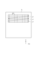
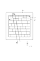
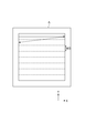
- FIG. 1 is a block diagram illustrating a configuration of an image generation device according to a first embodiment of the present invention. It is a conceptual diagram which shows the spatial modulation pattern of the illumination light prescribed
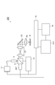
- FIG. 1 is a block diagram showing a configuration of an image generation apparatus 1 according to the first embodiment of the present invention.
- An image generation apparatus 1 shown in FIG. 1 scans illumination light based on a plurality of spatial modulation patterns on an object to be measured, which is an electric element such as a semiconductor device, and generates an electric signal generated from the object to be measured A accordingly.
- the image generation apparatus 1 includes a laser light source 3 that emits laser light, a laser scanner (laser scanning unit) 5, an electric signal detector (detection unit) 7 that detects an electric signal generated from the object A to be measured, and a laser.
- An optical system 9 that guides laser light from the light source 3 toward the object A to be measured, a laser output control unit (laser modulation unit) 11 that controls the output intensity of the laser light source 3, and the operation of the laser scanner 5 are controlled.
- An electrical signal imaging that images the electrical characteristics of the electrical signal detected by the electrical signal detector 7 and the modulation pattern control unit 15 that controls the spatial modulation pattern irradiated to the object A to be measured.
- Unit (signal generation unit) 17 and an image data calculation unit (image processing unit) 19 that generates a pattern image of the object A using the imaging signal generated by the electrical signal imaging unit 17.
- the optical system 9 includes a relay lens 21, a mirror 23, and an objective lens 25.
- the relay lens 21 is an optical system that efficiently guides the laser light whose irradiation angle is changed by the laser scanner 5 to the objective lens 25, and projects the exit pupil of the objective lens 25 onto the reflection surface of the laser scanner 5.
- the laser beam reflected by the laser scanner 5 has a role of reliably reaching the objective lens 25.
- the mirror 23 may not be used.
- the laser scanner 5 is an optical device that scans the irradiation position two-dimensionally by changing the traveling direction of the laser light. In other words, the laser scanner 5 changes the incident angle of the laser light incident on the relay lens 21 to change the irradiation position of the laser light irradiated through the optical system 9 on the surface of the object A to be measured. Scan in two dimensions.
- a galvanometer mirror having two mirrors whose rotation axes are orthogonal to each other and whose rotation angles can be electrically controlled can be used.
- a polygon mirror a MEMS (Micro Electro Mechanical System) mirror, an AOD (acousto-optic deflector), a resonant scanner (resonant galvanometer scanner), an EO scanner (electro-optic light deflector), etc. are employed.
- a MEMS Micro Electro Mechanical System
- AOD acousto-optic deflector
- a resonant scanner resonant galvanometer scanner
- an EO scanner electro-optic light deflector
- the intensity of the laser light output from the laser light source 3 is configured to be modulated by a control signal from the laser output control unit 11 connected to the laser light source 3, and the laser light to be measured by the laser scanner 5 is measured.
- the irradiation position on the surface of the object A is configured to be changeable by a control signal from the scanner control unit 13 connected to the laser scanner 5.
- a modulation pattern control unit 15 is connected to the laser output control unit 11 and the scanner control unit 13, and the modulation pattern control unit 15 emits illumination light based on a plurality of predetermined spatial modulation patterns on the object A to be measured.
- the laser output control unit 11 and the scanner control unit 13 are controlled so as to be scanned.
- the modulation pattern control unit 15 performs control so that the irradiation position of the laser beam is moved along the X-axis direction which is a predetermined direction along the plane of the object A to be measured.
- the irradiation intensity of the laser beam is modulated so that the intensity distribution in the axial direction periodically increases and decreases according to a trigonometric function (sin function or cos function).
- a trigonometric function sin function or cos function
- the strip-shaped irradiation pattern L1 periodically modulated with the width W1 along the X-axis direction is formed.
- the modulation pattern control unit 15 shifts the laser irradiation position in the direction along the Y axis perpendicular to the X axis, and then moves the laser light irradiation position in the X axis direction and modulates the laser light intensity.
- the formation of the strip-shaped irradiation pattern L1 is repeated under control. As a result, a spatial modulation pattern having a striped pattern with a desired pitch W1 along the Y-axis direction can be generated. Note that the intensity of the laser light may be modulated periodically by ON-OFF.
- the modulation pattern control unit 15 causes the laser beam intensity to gradually shift the spatial phase of the strip-shaped irradiation pattern L2 along the X axis between adjacent patterns in the Y axis direction. It is also possible to control the modulation. In this case, it is possible to generate a spatial modulation pattern that approximates a striped pattern having a desired pitch W2 that is inclined by a desired angle ⁇ 2 with respect to the Y-axis direction. Further, as shown in FIG. 4, the modulation pattern control unit 15 makes the irradiation intensity of the laser beam uniform during one scan of the laser beam along the X axis, and forms a plurality of strips arranged in the Y axis direction.
- a spatial modulation pattern having a striped pattern with a desired pitch W3 along the X-axis direction can be generated.
- the spatial modulation pattern is preferably a striped pattern having n-fold rotational symmetry (n is 3 or more).
- the electric signal detector 7 detects an electric signal such as a photovoltaic current generated from the measurement object A in accordance with the irradiation timing of the illumination light having the spatial modulation pattern as described above. For example, the electrical signal detector 7 detects a characteristic value such as a current value of a photovoltaic current generated in response to laser light irradiation as a voltage change between two terminals of the object A to be measured.
- the electrical signal imaging unit 17 is connected to the electrical signal detector 7 and the modulation pattern control unit 15 and images the characteristic values detected by the electrical signal detector 7. That is, the electrical signal imaging unit 17 specifies the irradiation position of the laser beam on the measurement object A when the characteristic value is detected as irradiation position information such as XY coordinates.
- the electric signal imaging unit 17 generates characteristic distribution information in which the irradiation position information is associated with the characteristic information regarding the characteristic value of the electric signal detected according to the irradiation of the laser beam at the corresponding irradiation position. To do. Furthermore, the electrical signal imaging unit 17 generates a two-dimensional characteristic image including a plurality of characteristic distribution information corresponding to each spatial modulation pattern irradiated to the object A to be measured. For example, the electrical signal imaging unit 17 generates a two-dimensional characteristic image signal in which each characteristic value is arranged for each coordinate on the object A to be measured. When the spatial modulation patterns as shown in FIGS. 2 to 4 are continuously formed in time, the electric signal imaging unit 17 generates a separate characteristic image for each spatial modulation pattern.
- the plurality of characteristic images generated by the electrical signal imaging unit 17 are subjected to image processing by the image data calculation unit 19.
- the image data calculation unit 19 irradiates the surface of the object A to be measured with a striped spatial modulation pattern along the Y-axis direction while changing the spatial phase at a desired frequency to obtain a plurality of characteristic images.
- the plurality of characteristic images obtained at that time are obtained as moire (interference fringe) components between the stripe pattern by the illumination light and the characteristic image resulting from the structure of the object A to be measured, and the space resulting from the fine structure of the object A to be measured.
- the high frequency component appears as moiré after being converted to a low frequency component.
- the image data calculation unit 19 uses the characteristic distribution obtained from the plurality of characteristic images, based on the frequency information of the irradiated spatial modulation pattern, and the original characteristic distribution resulting from the actual structure of the object A to be measured. Generate an image. Then, the image data calculation unit 19 irradiates a plurality of spatial modulation patterns along the four directions while changing the spatial phase at a desired frequency, and creates a plurality of characteristic distribution images by performing similar image processing. A high-resolution pattern image in which the resolution is increased in four directions can be generated from a plurality of characteristic distribution images.
- the intensity of the laser light emitted from the laser light source 3 is modulated by the laser output control unit 11, and at the same time the irradiation position of the object A to be measured by the laser scanner 5.
- the object to be measured A is irradiated while being scanned.
- the electrical signal detector 7 is controlled while the laser output control unit 11 and the laser scanner 5 are controlled by the modulation pattern control unit 15 such that illumination light of a plurality of two-dimensional spatial modulation patterns is irradiated on the object A to be measured.
- an electric signal generated from the object A to be measured is detected.
- the electrical signal imaging unit 17 corresponds to each spatial modulation pattern, information on the illumination light irradiation position and information on the characteristics of the electrical signal detected according to the illumination light irradiation at the irradiation position.
- the attached characteristic distribution information is generated, and a two-dimensional characteristic image is generated corresponding to each spatial modulation pattern.
- the image data calculation unit 19 uses the plurality of two-dimensional characteristic images to determine the object A to be measured. A pattern image is generated. This eliminates the need to pass through an optical system including an objective lens and an imaging lens when acquiring a pattern image from the object A, so that the resolution of the pattern image of the sample can be easily improved.
- a high-resolution pattern image of the object A can be easily obtained without requiring a complicated driving mechanism for driving a diffraction grating or the like. That is, in this embodiment, it is only necessary to mount a simple optical system and a laser scanner.
- the phase and orientation of the spatial modulation pattern of the illumination light applied to the object to be measured can be easily changed by the control of the modulation pattern control unit 15 to quickly obtain a high-resolution image at a desired position and orientation. be able to.
- SLM Surface Light Modulator
- the number of stripes at the resolution limit ⁇ 3 the number of pixels in the uniaxial direction is required.
- the number of pixels is further tripled to match the pixels to the stripe pitch.
- the conventional apparatus requires an expensive SLM.
- light transmission / reflection loss in the SLM, loss at pixel joints, zero-order light, and higher-order light also occur.
- the object A to be measured causes multiphoton absorption such as two-photon absorption, or generates second-order harmonics (SHG) For those that show nonlinear reactions, such reactions are likely to occur.
- multiphoton absorption such as two-photon absorption
- SHG second-order harmonics
- the laser output control unit 11 modulates the intensity of the laser light so as to change according to the trigonometric function, it is easy to form a spatial modulation pattern.
- FIG. 5 is a block diagram showing a configuration of the image generation apparatus 101 according to the second embodiment of the present invention.
- the image generating apparatus 101 shown in the figure irradiates a measurement object such as a semiconductor device with illumination light having a plurality of spatial modulation patterns, and detects reflected light generated from the measurement object A as an optical signal accordingly.
- This is an apparatus for obtaining a high-resolution pattern image of an object to be measured based on the characteristic distribution of the optical signal.
- the difference of the image generating apparatus 101 from the first embodiment is that an optical signal detector 107 and an optical signal imaging unit 117 are provided instead of the electrical signal detector 7 and the electrical signal imaging unit 17.
- the optical signal detector 107 detects reflected light or the like generated from the measurement object A as an optical signal.
- the optical signal detector 107 is a photoelectric converter such as a photomultiplier tube or a photoelectric tube that outputs a characteristic value such as the intensity of reflected light as an electric signal.
- the optical signal imaging unit 117 also includes characteristic information regarding the characteristic value of the optical signal detected by the optical signal detector 107, and irradiation position information of the laser light on the measurement object A when the characteristic value is detected. Is generated for each of the plurality of spatial modulation patterns from the characteristic distribution information associated with the two-dimensional characteristic image (characteristic image) including the plurality of characteristic distribution information.
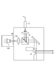
- FIG. 6 shows a detailed configuration around the optical signal detector 107 of the image generating apparatus 101.
- a beam splitter 31 is disposed between the laser scanner 5 and the exit of the laser light source 3 constituted by an optical fiber and the optical signal detector 107.
- This beam splitter 31 transmits the reflected light and scattered light from the object A to be measured incident through the laser scanner 5 and guides it to the optical signal detector 107, and at the same time reflects the laser light from the laser light source 3 to the laser.
- the light path of the reflected light and the scattered light is separated from the optical path of the laser light by being guided to the measured object A side via the scanner 5.
- a half mirror having a 1: 1 relationship between reflectance and transmittance, or one having a predetermined relationship such as 8: 2 is used.
- a polarization beam splitter can be used as the beam splitter 31.
- a quarter wavelength plate is inserted between the polarizing beam splitter and the objective lens 25.
- the reflected light When passing through the wave plate, the reflected light can be converted into linearly polarized light that is 90 degrees different from that at the time of incidence. As a result, the reflected light can be transmitted through the polarization beam splitter and guided to the optical signal detector 107 side.
- a spatial filter 35 and a condenser lens 33 are disposed between the optical signal detector 107 and the beam splitter 31.
- the spatial filter 35 is placed at a position conjugate with the end face of the fiber of the laser light source 3 to form a confocal optical system, and its filter diameter is substantially equal to the beam spot diameter formed on the face conjugate with the fiber end face. Is set.
- This spatial filter 35 blocks the reflection / scattering component from the portion out of focus of the reflected / scattering light returned from the object A to be measured through the optical system.
- the image generating apparatus 101 described above it is possible to acquire the characteristics of reflected / scattered light generated by the irradiation of the spatial modulation pattern onto the measurement object A as a pattern image with improved resolution on the measurement object. .
- the phase and orientation of the spatial modulation pattern of the illumination light applied to the object to be measured can be easily changed by the control of the modulation pattern control unit 15, and a high-resolution image image at a desired position and orientation can be quickly obtained. Obtainable.
- FIG. 7 is a block diagram showing a configuration of an image generation apparatus 201 according to the third embodiment of the present invention.
- the image generation apparatus 201 shown in the figure irradiates a measurement object such as a cell with excitation light of a plurality of spatial modulation patterns, and detects weak fluorescence generated from the measurement object A as an optical signal accordingly.
- This is an apparatus for obtaining a high-resolution pattern image of an object to be measured based on the characteristic distribution of the optical signal.
- the image generating apparatus 201 is different from the second embodiment in the configuration around the optical signal detector.
- a photoelectric converter such as a photomultiplier tube capable of outputting a characteristic value such as weak fluorescence intensity as an electric signal is used.
- a dichroic mirror 41 is disposed between the exit of the laser light source 3 and the optical signal detector 207 and the laser scanner 5 instead of the beam splitter.
- the dichroic mirror 41 transmits the fluorescence from the object A to be measured incident through the laser scanner 5 and guides it to the optical signal detector 207, and at the same time reflects the laser light from the laser light source 3 and passes through the laser scanner 5. Then, the fluorescent light path is separated from the laser light optical path by guiding it to the DUT A side.
- the dichroic mirror 41 has a function of reflecting excitation light toward the laser scanner 5 and transmitting fluorescence generated from the object A to be measured, and has a short wavelength reflection and a long wavelength transmission optical multilayer film. It is a mirror containing.
- an excitation wavelength selection filter 43 is provided between the laser light source 3 and the dichroic mirror 41.
- the excitation wavelength selection filter 43 is provided to select a wavelength that matches the characteristics of the laser light source 3 from the wavelength of the laser light source 3 in accordance with the fluorescence excitation characteristics of the object A to be measured.
- a barrier filter 45 is provided between the optical signal detector 207 and the dichroic mirror 41.
- the barrier filter 45 cuts the excitation light so that the excitation light does not reach the optical signal detector 207 when fluorescence is detected by the optical signal detector 207.
- This barrier filter absorbs and reflects the wavelength component of the excitation light, cuts it off and transmits the wavelength component of the fluorescence, and transmits only the wavelength component of the fluorescence. It is a band pass filter to be made.
- an image generating apparatus 201 it is possible to acquire the characteristics of the fluorescence generated by the irradiation of the spatial modulation pattern onto the object to be measured A as a pattern image with improved resolution on the object to be measured.
- the phase and orientation of the spatial modulation pattern of the illumination light applied to the object to be measured can be easily changed by the control of the modulation pattern control unit 15, and a high-resolution image image at a desired position and orientation can be quickly obtained. Obtainable.
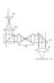
- a configuration as shown in FIG. 9 may be adopted as the configuration of the optical system for guiding the illumination light.
- an axicon 211 and a converter lens 212 may be inserted between the laser light source 3 and the laser scanner 5.
- the axicon 211 is a conical prism, and is an optical element that converts a parallel beam having a circular cross section emitted from the laser light source 3 into a beam having a circular cross section.
- the converter lens 212 is a lens that projects a ring-shaped beam emitted from the axicon 211 onto the laser scanner 5 in a circumferential shape.
- the laser light source 3 of the image generating apparatuses 1, 101, 201 as shown in FIG. 10, a configuration capable of observing multiphoton excitation such as two-photon excitation in the object A to be measured may be employed.
- the laser light source 3 employs a configuration comprising an ultrashort pulse laser 3a that includes a wavelength capable of two-photon absorption in the DUT A as an emission wavelength, and a laser modulator 3b that modulates the output thereof.
- An excitation wavelength selection filter 301 for selecting a desired wavelength component from the laser light is inserted between the laser light source 3 and the laser scanner 5.
- Two-photon excitation is a phenomenon in which electrons are excited by two photons having a wavelength twice that of the original excitation light to emit fluorescence.
- the excitation wavelength selection filter 301 functions to transmit light having a wavelength twice that of the excitation wavelength of the fluorescent sample. If such a laser light source 3 is used, it is possible to use light having a long wavelength and low energy, so that damage to the sample is suppressed, and the sample has good permeability, so that the light can reach a deep place and has a feature of two-photon absorption. Excitation that makes use of the three-dimensional locality of an excitation point can be performed. In addition, as a feature of two-photon excitation, a resolution equivalent to that of a single wavelength can be obtained even though the wavelength is doubled, and higher resolution can be expected by combining with this technique. When the configuration of the laser light source 3 shown in FIG.
- the dichroic mirror 41 and the barrier filter 45 need to be changed to those having different functions. That is, the dichroic mirror 41 has a function of reflecting the long wavelength excitation light incident from the laser light source 3 side toward the laser scanner 5 and transmitting the short wavelength fluorescence generated from the object A to be measured. A dichroic mirror having optical characteristics of long wavelength reflection and short wavelength transmission is used.
- the barrier filter 45 is a low-pass filter having a property of cutting by absorbing and reflecting the long-wavelength component of the excitation light and transmitting the short-wavelength component of the fluorescence, and having a short-wavelength transmission property, A bandpass filter that transmits only the wavelength component is used.
- the detection unit detects an electrical signal generated from the object to be measured, and the signal generation unit generates characteristic distribution information in which illumination light irradiation position information and characteristic information related to the characteristic of the electric signal are associated with each other. Is preferable. In this case, it is possible to obtain the electrical characteristics such as the photocurrent value generated by irradiating the object to be measured with the laser light as a pattern image in the object to be measured, and to improve the accuracy of the characteristic analysis of the electric element such as a semiconductor. Can be improved.
- the detection unit detects an optical signal generated from the object to be measured, and the signal generation unit generates characteristic distribution information in which the irradiation position information of the illumination light and the characteristic information regarding the characteristic of the optical signal are associated with each other. It is also suitable. By adopting such a configuration, it is possible to acquire the characteristics of light such as reflected light and fluorescence generated with irradiation of the laser beam to the object to be measured as a pattern image with improved resolution in the object to be measured.
- the laser light from the laser light source includes a wavelength capable of multiphoton absorption in the object to be measured.
- the effect on the object to be measured is equivalent to a spot shape that is squared for two photons and cubed for three photons, and the generated signal is effectively scanned with a small spot.
- the modulation stripes can be made finer, and the resolution can be further improved.
- the laser modulator modulates the intensity of the laser light so as to change according to a trigonometric function. If such a laser modulation unit is provided, it is easy to form a spatial modulation pattern.
- the present invention uses an image generating apparatus that generates an image by irradiating a measured object with spatially modulated light, and can obtain a pattern image of a sample with improved resolution with a simple apparatus configuration. It is.
Landscapes
- Physics & Mathematics (AREA)
- General Physics & Mathematics (AREA)
- Chemical & Material Sciences (AREA)
- Analytical Chemistry (AREA)
- Optics & Photonics (AREA)
- Engineering & Computer Science (AREA)
- Multimedia (AREA)
- Microscoopes, Condenser (AREA)
- Investigating Or Analysing Materials By Optical Means (AREA)
- Investigating, Analyzing Materials By Fluorescence Or Luminescence (AREA)
Abstract
Description
図1は、本発明の第1実施形態に係る画像生成装置1の構成を示すブロック図である。図1に示す画像生成装置1は、半導体デバイス等の電気素子である被測定物に対して複数の空間変調パターンに基づいて照明光を走査し、それに応じて被測定物Aから生じる電気信号の複数の特性分布を検出し、それらの複数の特性分布を基にして被測定物の高解像度パターン像を得るための装置である。この画像生成装置1は、レーザ光を出射するレーザ光源3と、レーザスキャナ(レーザ走査部)5と、被測定物Aから生じる電気信号を検出する電気信号検出器(検出部)7と、レーザ光源3からのレーザ光を被測定物Aに向けて導光する光学系9と、レーザ光源3の出力強度を制御するレーザ出力制御部(レーザ変調部)11と、レーザスキャナ5の動作を制御するスキャナ制御部13と、被測定物Aに照射される空間変調パターンを制御する変調パターン制御部15と、電気信号検出器7によって検出された電気信号の電気特性を画像化する電気信号画像化部(信号生成部)17と、電気信号画像化部17によって生成された画像化信号を用いて被測定物Aのパターン画像を生成する画像データ演算部(画像処理部)19とを備えている。
図5は、本発明の第2実施形態に係る画像生成装置101の構成を示すブロック図である。同図に示す画像生成装置101は、半導体デバイス等の被測定物に対して複数の空間変調パターンの照明光を照射し、それに応じて被測定物Aから生じる反射光を光信号として検出し、その光信号の特性分布を基にして被測定物の高解像度パターン像を得るための装置である。この画像生成装置101の第1実施形態との相違点は、電気信号検出器7及び電気信号画像化部17の代わりに、光信号検出器107及び光信号画像化部117を備える点である。
図7は、本発明の第3実施形態に係る画像生成装置201の構成を示すブロック図である。同図に示す画像生成装置201は、細胞等の被測定物に対して複数の空間変調パターンの励起光を照射し、それに応じて被測定物Aから生じる微弱な蛍光を光信号として検出し、その光信号の特性分布を基にして被測定物の高解像度パターン像を得るための装置である。この画像生成装置201は、光信号検出器の周辺の構成が第2実施形態と異なる。
なお、図10に示したレーザ光源3の構成を、画像生成装置201と組み合わせて使用した場合には、ダイクロイックミラー41及びバリアフィルタ45をその機能が異なるものに変更する必要がある。すなわち、ダイクロイックミラー41としては、レーザ光源3側から入射した長波長の励起光をレーザスキャナ5に向けて反射し、被測定物Aから生じた短波長の蛍光を透過するような機能を有し、長波長反射および短波長透過の光学特性を有するダイクロイックミラーが使用される。また、バリアフィルタ45としては、励起光の長波長成分を吸収、反射することによりカットし、蛍光の短波長成分を透過させる性質を有し、短波長透過性を有するローパスフィルタ、又は、蛍光の波長成分のみを透過させるバンドパスフィルタが使用される。
Claims (5)
- 被測定物の画像を生成する画像生成装置であって、
レーザ光を出射するレーザ光源と、
前記レーザ光の強度を変調させるレーザ変調部と、
前記レーザ光の前記被測定物への照射位置を走査するレーザ走査部と、
前記被測定物に複数の空間変調パターンの照明光を照射するように、前記レーザ変調部及び前記レーザ走査部を制御する制御部と、
前記複数の空間変調パターンの照明光の照射に応じて前記被測定物から生じる信号を検出する検出部と、
前記制御部によって制御された前記照明光の照射位置に関する照射位置情報と、前記照射位置における前記レーザ光の照射に応じて前記検出部によって検出された信号の特性に関する特性情報とが対応付けられた特性分布情報を生成し、前記空間変調パターンに対応して複数の前記特性分布情報を含む2次元特性画像を生成する信号生成部と、
複数の前記空間変調パターンに対応して生成した複数の前記2次元特性画像を基に、前記被測定物のパターン画像を生成する画像処理部と、
を備えることを特徴とする画像生成装置。 - 前記検出部は、前記被測定物から生じる電気信号を検出し、
前記信号生成部は、前記照明光の前記照射位置情報と、前記電気信号の特性に関する特性情報とが対応付けられた特性分布情報を生成する、
ことを特徴とする請求項1記載の画像生成装置。 - 前記検出部は、前記被測定物から生じる光信号を検出し、
前記信号生成部は、前記照明光の前記照射位置情報と、前記光信号の特性に関する特性情報とが対応付けられた特性分布情報を生成する、
ことを特徴とする請求項1記載の画像生成装置。 - 前記レーザ光源からの前記レーザ光は、被測定物において多光子吸収が可能な波長を含む、
ことを特徴とする請求項1~3のいずれか1項に記載の画像生成装置。 - 前記レーザ変調部は、前記レーザ光の強度を三角関数に従って変化するように変調させる、
ことを特徴とする請求項1~4のいずれか1項に記載の画像生成装置。
Priority Applications (4)
| Application Number | Priority Date | Filing Date | Title |
|---|---|---|---|
| EP11798071.4A EP2587298A4 (en) | 2010-06-23 | 2011-06-17 | IMAGE GENERATING DEVICE |
| KR1020127033467A KR20130092429A (ko) | 2010-06-23 | 2011-06-17 | 화상 생성 장치 |
| CN2011800307103A CN102947741A (zh) | 2010-06-23 | 2011-06-17 | 图像生成装置 |
| US13/806,486 US20130120563A1 (en) | 2010-06-23 | 2011-06-17 | Image generation device |
Applications Claiming Priority (2)
| Application Number | Priority Date | Filing Date | Title |
|---|---|---|---|
| JP2010-142882 | 2010-06-23 | ||
| JP2010142882A JP2012008261A (ja) | 2010-06-23 | 2010-06-23 | 画像生成装置 |
Publications (1)
| Publication Number | Publication Date |
|---|---|
| WO2011162187A1 true WO2011162187A1 (ja) | 2011-12-29 |
Family
ID=45371374
Family Applications (1)
| Application Number | Title | Priority Date | Filing Date |
|---|---|---|---|
| PCT/JP2011/063976 Ceased WO2011162187A1 (ja) | 2010-06-23 | 2011-06-17 | 画像生成装置 |
Country Status (7)
| Country | Link |
|---|---|
| US (1) | US20130120563A1 (ja) |
| EP (1) | EP2587298A4 (ja) |
| JP (1) | JP2012008261A (ja) |
| KR (1) | KR20130092429A (ja) |
| CN (1) | CN102947741A (ja) |
| TW (1) | TW201213849A (ja) |
| WO (1) | WO2011162187A1 (ja) |
Cited By (2)
| Publication number | Priority date | Publication date | Assignee | Title |
|---|---|---|---|---|
| CN103054557A (zh) * | 2013-01-08 | 2013-04-24 | 白宇 | 云纹图像成像装置 |
| CN110007453A (zh) * | 2019-05-13 | 2019-07-12 | 中国科学院生物物理研究所 | 一种多照明模式的荧光信号测量装置及其测量方法和应用 |
Families Citing this family (13)
| Publication number | Priority date | Publication date | Assignee | Title |
|---|---|---|---|---|
| JP6166032B2 (ja) | 2012-11-06 | 2017-07-19 | 浜松ホトニクス株式会社 | 半導体デバイス検査装置及び半導体デバイス検査方法 |
| JP2015114420A (ja) | 2013-12-10 | 2015-06-22 | ソニー株式会社 | 画像取得装置及び画像取得方法 |
| JP6357317B2 (ja) * | 2014-01-30 | 2018-07-11 | オリンパス株式会社 | 顕微鏡照明装置、顕微鏡照明方法および顕微鏡 |
| US9690085B2 (en) * | 2014-01-30 | 2017-06-27 | Olympus Corporation | Microscope illumination apparatus, microscope, and microscope illumination method |
| JP5996687B2 (ja) | 2015-02-10 | 2016-09-21 | 浜松ホトニクス株式会社 | 検査装置及び検査方法 |
| KR101759875B1 (ko) * | 2015-06-24 | 2017-07-20 | 주식회사 엘지실트론 | 웨이퍼 연마장치의 스캔장치 및 스캔시스템 |
| US10048485B2 (en) * | 2015-08-28 | 2018-08-14 | Panasonic Intellectual Property Management Co., Ltd. | Image output device, image transmission device, image reception device, image output method, and non-transitory recording medium |
| CH711570B1 (de) * | 2015-09-28 | 2019-02-15 | Besi Switzerland Ag | Vorrichtung für die Montage von Bauelementen auf einem Substrat. |
| JP6632327B2 (ja) * | 2015-10-30 | 2020-01-22 | 浜松ホトニクス株式会社 | 画像生成方法、画像生成装置、画像生成プログラム及び記録媒体 |
| KR102543948B1 (ko) | 2016-05-17 | 2023-06-15 | 삼성전자주식회사 | 클럭 신호 생성기 및 기판 검사 장치 |
| KR101934956B1 (ko) * | 2017-10-18 | 2019-03-18 | 고려대학교 산학협력단 | 구조 조명과 위상 검출을 이용한 단분자 중심위치 측정 장치 및 방법 |
| JP7000197B2 (ja) * | 2018-02-16 | 2022-01-19 | 浜松ホトニクス株式会社 | 濃度測定方法及び濃度測定装置 |
| JP7395511B2 (ja) * | 2019-01-16 | 2023-12-11 | 株式会社小糸製作所 | イメージング装置、その演算処理装置、車両用灯具、車両、センシング方法 |
Citations (5)
| Publication number | Priority date | Publication date | Assignee | Title |
|---|---|---|---|---|
| JPH05503149A (ja) * | 1989-11-14 | 1993-05-27 | コーネル・リサーチ・ファンデーション・インコーポレイテッド | 2光子レーザ走査顕微鏡 |
| JPH09230246A (ja) * | 1996-02-22 | 1997-09-05 | Olympus Optical Co Ltd | 走査型光学顕微鏡 |
| JP2001117010A (ja) | 1999-10-21 | 2001-04-27 | Olympus Optical Co Ltd | 光学装置 |
| JP2007199572A (ja) | 2006-01-30 | 2007-08-09 | Nikon Corp | 顕微鏡装置 |
| JP2009510499A (ja) * | 2005-09-29 | 2009-03-12 | カール ツァイス マイクロイメージング ゲーエムベーハー | 対象物の画像を生成するための装置および方法 |
Family Cites Families (15)
| Publication number | Priority date | Publication date | Assignee | Title |
|---|---|---|---|---|
| JP2931226B2 (ja) * | 1995-01-26 | 1999-08-09 | 浜松ホトニクス株式会社 | 光帰還式光検出装置 |
| US5708371A (en) * | 1995-03-16 | 1998-01-13 | Mitsubishi Denki Kabushiki Kaisha | Scanning photoinduced current analyzer capable of detecting photoinduced current in nonbiased specimen |
| JP3411780B2 (ja) * | 1997-04-07 | 2003-06-03 | レーザーテック株式会社 | レーザ顕微鏡及びこのレーザ顕微鏡を用いたパターン検査装置 |
| US6078183A (en) * | 1998-03-03 | 2000-06-20 | Sandia Corporation | Thermally-induced voltage alteration for integrated circuit analysis |
| JP2000292705A (ja) * | 1999-04-05 | 2000-10-20 | Olympus Optical Co Ltd | 走査型顕微鏡 |
| US20070196815A1 (en) * | 2000-08-02 | 2007-08-23 | Jason Lappe | Positive Selection Procedure for Optically Directed Selection of Cells |
| JP2003075514A (ja) * | 2001-09-06 | 2003-03-12 | Matsushita Electric Ind Co Ltd | 検査装置および検査方法 |
| DE602005007403D1 (de) * | 2004-03-25 | 2008-07-24 | Olympus Corp | Scannendes konfokales Mikroskop |
| JP4425098B2 (ja) * | 2004-09-06 | 2010-03-03 | 浜松ホトニクス株式会社 | 蛍光顕微鏡および蛍光相関分光解析装置 |
| JP4597744B2 (ja) * | 2004-11-08 | 2010-12-15 | 株式会社トプコン | 光画像計測装置及び光画像計測方法 |
| US7326899B2 (en) * | 2005-07-11 | 2008-02-05 | Olympus Corporation | Laser scanning microscope and image acquiring method of laser scanning microscope |
| US7485875B2 (en) * | 2005-07-22 | 2009-02-03 | Carl Zeiss Microimaging Gmbh | Resolution-enhanced luminescence microscopy |
| WO2007109861A1 (en) * | 2006-03-29 | 2007-10-04 | The University Of Queensland | Super resolution microscopy |
| US7838818B2 (en) * | 2006-06-22 | 2010-11-23 | Olympus Corporation | Light-stimulus illumination apparatus which scans light-stimulus laser light in a direction intersecting an optical axis |
| WO2008081374A2 (en) * | 2006-12-28 | 2008-07-10 | Koninklijke Philips Electronics N.V. | Reflection or single scattering spectroscopy and imaging |
-
2010
- 2010-06-23 JP JP2010142882A patent/JP2012008261A/ja active Pending
-
2011
- 2011-06-17 EP EP11798071.4A patent/EP2587298A4/en not_active Withdrawn
- 2011-06-17 WO PCT/JP2011/063976 patent/WO2011162187A1/ja not_active Ceased
- 2011-06-17 CN CN2011800307103A patent/CN102947741A/zh active Pending
- 2011-06-17 KR KR1020127033467A patent/KR20130092429A/ko not_active Withdrawn
- 2011-06-17 US US13/806,486 patent/US20130120563A1/en not_active Abandoned
- 2011-06-23 TW TW100122056A patent/TW201213849A/zh unknown
Patent Citations (5)
| Publication number | Priority date | Publication date | Assignee | Title |
|---|---|---|---|---|
| JPH05503149A (ja) * | 1989-11-14 | 1993-05-27 | コーネル・リサーチ・ファンデーション・インコーポレイテッド | 2光子レーザ走査顕微鏡 |
| JPH09230246A (ja) * | 1996-02-22 | 1997-09-05 | Olympus Optical Co Ltd | 走査型光学顕微鏡 |
| JP2001117010A (ja) | 1999-10-21 | 2001-04-27 | Olympus Optical Co Ltd | 光学装置 |
| JP2009510499A (ja) * | 2005-09-29 | 2009-03-12 | カール ツァイス マイクロイメージング ゲーエムベーハー | 対象物の画像を生成するための装置および方法 |
| JP2007199572A (ja) | 2006-01-30 | 2007-08-09 | Nikon Corp | 顕微鏡装置 |
Non-Patent Citations (1)
| Title |
|---|
| See also references of EP2587298A4 |
Cited By (4)
| Publication number | Priority date | Publication date | Assignee | Title |
|---|---|---|---|---|
| CN103054557A (zh) * | 2013-01-08 | 2013-04-24 | 白宇 | 云纹图像成像装置 |
| CN110007453A (zh) * | 2019-05-13 | 2019-07-12 | 中国科学院生物物理研究所 | 一种多照明模式的荧光信号测量装置及其测量方法和应用 |
| CN110007453B (zh) * | 2019-05-13 | 2023-11-21 | 中国科学院生物物理研究所 | 一种多照明模式的荧光信号测量装置及其测量方法和应用 |
| US12474268B2 (en) | 2019-05-13 | 2025-11-18 | Institute Of Biophysics, Chinese Academy Of Sciences | Device and method for measuring fluorescence signal in multi-illumination mode, and use of the method |
Also Published As
| Publication number | Publication date |
|---|---|
| JP2012008261A (ja) | 2012-01-12 |
| TW201213849A (en) | 2012-04-01 |
| KR20130092429A (ko) | 2013-08-20 |
| CN102947741A (zh) | 2013-02-27 |
| EP2587298A4 (en) | 2014-03-05 |
| EP2587298A1 (en) | 2013-05-01 |
| US20130120563A1 (en) | 2013-05-16 |
Similar Documents
| Publication | Publication Date | Title |
|---|---|---|
| JP2012008261A (ja) | 画像生成装置 | |
| WO2011162186A1 (ja) | 画像生成装置 | |
| CA2282416C (en) | Light sensing device | |
| JP3996783B2 (ja) | 走査型顕微鏡及び走査型顕微鏡用モジュール | |
| JP6346615B2 (ja) | 光学顕微鏡および顕微鏡観察方法 | |
| US9081186B2 (en) | Microscope device for generating images of a specimen using phase distribution of light | |
| JP6738254B2 (ja) | 欠陥検出装置及び欠陥観察装置 | |
| CN102735617A (zh) | 一种超分辨显微方法和装置 | |
| WO2012070314A1 (ja) | 顕微鏡用分光分析装置、光軸ズレ補正装置、分光装置とそれを用いた顕微鏡 | |
| CN107092086A (zh) | 基于相位调制的激光扫描饱和结构光照明的显微方法及装置 | |
| JP2009109788A (ja) | レーザー走査型顕微鏡 | |
| JP6210754B2 (ja) | 走査型光学顕微鏡 | |
| US10690897B2 (en) | Laser scanning microscope apparatus | |
| EP3583459A1 (en) | Structured illumination scanning microscopy | |
| JP6253395B2 (ja) | 画像生成システム | |
| US20050253056A1 (en) | Optical stimulation apparatus and optical-scanning examination apparatus | |
| JP2013205231A (ja) | ブリルアン散乱顕微鏡 | |
| WO2017213171A1 (ja) | 光学情報検知装置及び顕微鏡システム | |
| CN102866137B (zh) | 一种二维超分辨显微方法和装置 | |
| US9924115B2 (en) | Apparatus and method for three-dimensional infrared imaging of surfaces | |
| WO2018084271A1 (ja) | 蛍光観察装置 | |
| JP6673497B2 (ja) | 蛍光観察装置 | |
| WO2017082357A1 (ja) | 超解像顕微鏡 | |
| JP4009620B2 (ja) | 顕微鏡装置 | |
| JP5454942B2 (ja) | 分光装置とそれを用いた顕微鏡 |
Legal Events
| Date | Code | Title | Description |
|---|---|---|---|
| WWE | Wipo information: entry into national phase |
Ref document number: 201180030710.3 Country of ref document: CN |
|
| 121 | Ep: the epo has been informed by wipo that ep was designated in this application |
Ref document number: 11798071 Country of ref document: EP Kind code of ref document: A1 |
|
| ENP | Entry into the national phase |
Ref document number: 20127033467 Country of ref document: KR Kind code of ref document: A |
|
| NENP | Non-entry into the national phase |
Ref country code: DE |
|
| WWE | Wipo information: entry into national phase |
Ref document number: 2011798071 Country of ref document: EP |
|
| WWE | Wipo information: entry into national phase |
Ref document number: 13806486 Country of ref document: US |