WO2012002143A1 - 低融点ガラス組成物及びそれを用いた導電性ペースト材料 - Google Patents
低融点ガラス組成物及びそれを用いた導電性ペースト材料 Download PDFInfo
- Publication number
- WO2012002143A1 WO2012002143A1 PCT/JP2011/063590 JP2011063590W WO2012002143A1 WO 2012002143 A1 WO2012002143 A1 WO 2012002143A1 JP 2011063590 W JP2011063590 W JP 2011063590W WO 2012002143 A1 WO2012002143 A1 WO 2012002143A1
- Authority
- WO
- WIPO (PCT)
- Prior art keywords
- glass
- conductive paste
- melting
- lead
- low
- Prior art date
- Legal status (The legal status is an assumption and is not a legal conclusion. Google has not performed a legal analysis and makes no representation as to the accuracy of the status listed.)
- Ceased
Links
Images
Classifications
-
- C—CHEMISTRY; METALLURGY
- C03—GLASS; MINERAL OR SLAG WOOL
- C03C—CHEMICAL COMPOSITION OF GLASSES, GLAZES OR VITREOUS ENAMELS; SURFACE TREATMENT OF GLASS; SURFACE TREATMENT OF FIBRES OR FILAMENTS MADE FROM GLASS, MINERALS OR SLAGS; JOINING GLASS TO GLASS OR OTHER MATERIALS
- C03C8/00—Enamels; Glazes; Fusion seal compositions being frit compositions having non-frit additions
- C03C8/02—Frit compositions, i.e. in a powdered or comminuted form
-
- H—ELECTRICITY
- H10—SEMICONDUCTOR DEVICES; ELECTRIC SOLID-STATE DEVICES NOT OTHERWISE PROVIDED FOR
- H10F—INORGANIC SEMICONDUCTOR DEVICES SENSITIVE TO INFRARED RADIATION, LIGHT, ELECTROMAGNETIC RADIATION OF SHORTER WAVELENGTH OR CORPUSCULAR RADIATION
- H10F77/00—Constructional details of devices covered by this subclass
-
- C—CHEMISTRY; METALLURGY
- C03—GLASS; MINERAL OR SLAG WOOL
- C03C—CHEMICAL COMPOSITION OF GLASSES, GLAZES OR VITREOUS ENAMELS; SURFACE TREATMENT OF GLASS; SURFACE TREATMENT OF FIBRES OR FILAMENTS MADE FROM GLASS, MINERALS OR SLAGS; JOINING GLASS TO GLASS OR OTHER MATERIALS
- C03C3/00—Glass compositions
- C03C3/04—Glass compositions containing silica
- C03C3/062—Glass compositions containing silica with less than 40% silica by weight
- C03C3/064—Glass compositions containing silica with less than 40% silica by weight containing boron
-
- C—CHEMISTRY; METALLURGY
- C03—GLASS; MINERAL OR SLAG WOOL
- C03C—CHEMICAL COMPOSITION OF GLASSES, GLAZES OR VITREOUS ENAMELS; SURFACE TREATMENT OF GLASS; SURFACE TREATMENT OF FIBRES OR FILAMENTS MADE FROM GLASS, MINERALS OR SLAGS; JOINING GLASS TO GLASS OR OTHER MATERIALS
- C03C3/00—Glass compositions
- C03C3/04—Glass compositions containing silica
- C03C3/062—Glass compositions containing silica with less than 40% silica by weight
- C03C3/064—Glass compositions containing silica with less than 40% silica by weight containing boron
- C03C3/066—Glass compositions containing silica with less than 40% silica by weight containing boron containing zinc
-
- C—CHEMISTRY; METALLURGY
- C03—GLASS; MINERAL OR SLAG WOOL
- C03C—CHEMICAL COMPOSITION OF GLASSES, GLAZES OR VITREOUS ENAMELS; SURFACE TREATMENT OF GLASS; SURFACE TREATMENT OF FIBRES OR FILAMENTS MADE FROM GLASS, MINERALS OR SLAGS; JOINING GLASS TO GLASS OR OTHER MATERIALS
- C03C8/00—Enamels; Glazes; Fusion seal compositions being frit compositions having non-frit additions
- C03C8/02—Frit compositions, i.e. in a powdered or comminuted form
- C03C8/04—Frit compositions, i.e. in a powdered or comminuted form containing zinc
-
- C—CHEMISTRY; METALLURGY
- C03—GLASS; MINERAL OR SLAG WOOL
- C03C—CHEMICAL COMPOSITION OF GLASSES, GLAZES OR VITREOUS ENAMELS; SURFACE TREATMENT OF GLASS; SURFACE TREATMENT OF FIBRES OR FILAMENTS MADE FROM GLASS, MINERALS OR SLAGS; JOINING GLASS TO GLASS OR OTHER MATERIALS
- C03C8/00—Enamels; Glazes; Fusion seal compositions being frit compositions having non-frit additions
- C03C8/14—Glass frit mixtures having non-frit additions, e.g. opacifiers, colorants, mill-additions
- C03C8/18—Glass frit mixtures having non-frit additions, e.g. opacifiers, colorants, mill-additions containing free metals
-
- H—ELECTRICITY
- H01—ELECTRIC ELEMENTS
- H01B—CABLES; CONDUCTORS; INSULATORS; SELECTION OF MATERIALS FOR THEIR CONDUCTIVE, INSULATING OR DIELECTRIC PROPERTIES
- H01B1/00—Conductors or conductive bodies characterised by the conductive materials; Selection of materials as conductors
- H01B1/20—Conductive material dispersed in non-conductive organic material
- H01B1/22—Conductive material dispersed in non-conductive organic material the conductive material comprising metals or alloys
-
- H—ELECTRICITY
- H01—ELECTRIC ELEMENTS
- H01B—CABLES; CONDUCTORS; INSULATORS; SELECTION OF MATERIALS FOR THEIR CONDUCTIVE, INSULATING OR DIELECTRIC PROPERTIES
- H01B3/00—Insulators or insulating bodies characterised by the insulating materials; Selection of materials for their insulating or dielectric properties
- H01B3/02—Insulators or insulating bodies characterised by the insulating materials; Selection of materials for their insulating or dielectric properties mainly consisting of inorganic substances
- H01B3/08—Insulators or insulating bodies characterised by the insulating materials; Selection of materials for their insulating or dielectric properties mainly consisting of inorganic substances quartz; glass; glass wool; slag wool; vitreous enamels
- H01B3/087—Chemical composition of glass
-
- H—ELECTRICITY
- H10—SEMICONDUCTOR DEVICES; ELECTRIC SOLID-STATE DEVICES NOT OTHERWISE PROVIDED FOR
- H10F—INORGANIC SEMICONDUCTOR DEVICES SENSITIVE TO INFRARED RADIATION, LIGHT, ELECTROMAGNETIC RADIATION OF SHORTER WAVELENGTH OR CORPUSCULAR RADIATION
- H10F77/00—Constructional details of devices covered by this subclass
- H10F77/20—Electrodes
- H10F77/206—Electrodes for devices having potential barriers
- H10F77/211—Electrodes for devices having potential barriers for photovoltaic cells
-
- Y—GENERAL TAGGING OF NEW TECHNOLOGICAL DEVELOPMENTS; GENERAL TAGGING OF CROSS-SECTIONAL TECHNOLOGIES SPANNING OVER SEVERAL SECTIONS OF THE IPC; TECHNICAL SUBJECTS COVERED BY FORMER USPC CROSS-REFERENCE ART COLLECTIONS [XRACs] AND DIGESTS
- Y02—TECHNOLOGIES OR APPLICATIONS FOR MITIGATION OR ADAPTATION AGAINST CLIMATE CHANGE
- Y02E—REDUCTION OF GREENHOUSE GAS [GHG] EMISSIONS, RELATED TO ENERGY GENERATION, TRANSMISSION OR DISTRIBUTION
- Y02E10/00—Energy generation through renewable energy sources
- Y02E10/50—Photovoltaic [PV] energy
Definitions
- the present invention relates to a low-melting-point glass composition that is suitable for a lead-free conductive paste material that has good electrical characteristics and has good adhesion to a silicon semiconductor substrate, particularly in electrodes formed in crystalline silicon solar cells. .
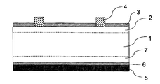
- a solar cell element as shown in FIG. 1 As an electronic component using a semiconductor silicon substrate, a solar cell element as shown in FIG. 1 is known. As shown in FIG. 1, the solar cell element is formed by forming an n-type semiconductor silicon layer 2 on the light-receiving surface side of a p-type semiconductor silicon substrate 1 having a thickness of about 200 ⁇ m, and nitriding to increase the light-receiving efficiency on the light-receiving surface side surface.
- An antireflection film 3 such as a silicon film, and a surface electrode 4 connected to the semiconductor are formed on the antireflection film 3.
- An aluminum electrode layer 5 is uniformly formed on the back side of the p-type semiconductor silicon substrate 1.
- the aluminum electrode layer 5 is generally formed by applying an aluminum paste material composed of an aluminum powder, glass frit, an organic vehicle containing a binder such as ethyl cellulose or acrylic resin by screen printing or the like, and having a temperature of about 600 to 900 ° C. It is formed by baking for a short time.
- an aluminum paste material composed of an aluminum powder, glass frit, an organic vehicle containing a binder such as ethyl cellulose or acrylic resin by screen printing or the like, and having a temperature of about 600 to 900 ° C. It is formed by baking for a short time.
- the p + layer 7 has an effect of suppressing loss due to recombination of carriers generated by the photovoltaic effect of the pn junction, and contributes to improvement in conversion efficiency of the solar cell element.
- the lead component is an important component for making the glass have a low melting point, it has a great adverse effect on the human body and the environment.
- the glass frit disclosed in Japanese Patent Application Laid-Open Nos. 2007-59380 and 2003-165744 has a problem that it contains a lead component.
- the present invention relates to a conductive paste for a solar cell using a silicon semiconductor substrate, wherein the composition of the low-melting glass contained in the paste is substantially free of a lead component and contains 2 to 10% of SiO 2 by weight, B 2 O 3 18-30%, Al 2 O 3 0-10%, ZnO 0-25%, RO (MgO + CaO + SrO + BaO) 20-50%, R 2 O (Li 2 O + Na 2 O + K 2 O)
- a conductive paste material characterized by being a SiO 2 —B 2 O 3 —ZnO—RO—R 2 O-based lead-free low-melting glass containing 10 to 17%.
- the lead-free low-melting glass has a thermal expansion coefficient at 30 ° C. to 300 ° C. of (100 to 150) ⁇ 10 ⁇ 7 / ° C. and a softening point of 400 ° C. to 550 ° C. Paste material.
- an electronic material substrate characterized by using the above conductive paste material.
- a conductive paste material containing the lead-free low melting point glass frit of the present invention By using a conductive paste material containing the lead-free low melting point glass frit of the present invention, a high BSF effect can be obtained. Also, good adhesion with the silicon semiconductor substrate can be obtained. Furthermore, since it does not substantially contain a lead component, there is no harmful effect on the human body and the environment.
- the conductive paste material of the present invention contains glass frit in addition to an organic vehicle containing aluminum powder and a binder such as ethyl cellulose or acrylic resin, the glass frit substantially does not contain a lead component, and contains SiO 2 by weight%. 2 ⁇ 10%, B 2 O 3 18 to 30% of Al 2 O 3 0 ⁇ 10% , the ZnO 0 ⁇ 25% RO a (MgO + CaO + SrO + BaO ) 20 ⁇ 50%, R 2 O (Li 2 O + Na 2 It is characterized by being a SiO 2 —B 2 O 3 —ZnO—RO—R 2 O-based lead-free low-melting glass containing 10 to 17% of O + K 2 O).
- SiO 2 is a glass-forming component, and when it coexists with B 2 O 3 which is another glass-forming component, a stable glass can be formed.
- the content is within the range of% by weight (the same applies to the following). If it exceeds 10%, the softening point of the glass will increase, making the formability and workability difficult. More preferably, it is in the range of 4 to 9%.
- B 2 O 3 is a glass-forming component, facilitates glass melting, suppresses an excessive increase in the thermal expansion coefficient of glass, gives moderate fluidity to glass during baking, and lowers the dielectric constant of glass It is.
- the glass is contained in the range of 18 to 30%. If it is less than 18%, the fluidity of the glass becomes insufficient and the sinterability is impaired. On the other hand, if it exceeds 30%, the stability of the glass is lowered. More preferably, it is in the range of 19 to 29%.
- Al 2 O 3 is a component that suppresses and stabilizes crystallization of glass. It is preferably contained in the range of 0 to 10% in the glass. If it exceeds 10%, the softening point of the glass rises, and formability and workability become difficult.
- ZnO lowers the softening point of the glass and is contained in the glass in the range of 0 to 25%. If it exceeds 25%, the glass becomes unstable and crystals tend to be formed. Preferably it is 0 to 23% of range.
- RO MgO + CaO + SrO + BaO
- R 2 O Li 2 O, Na 2 O, K 2 O
- R 2 O lowers the softening point of the glass, imparts moderate fluidity, and adjusts the thermal expansion coefficient to an appropriate range.
- the range of 10 to 17% To contain. If it is less than 10%, the softening point of the glass is not sufficiently lowered, and the sinterability is impaired. On the other hand, if it exceeds 17%, the thermal expansion coefficient is excessively increased. More preferably, it is in the range of 12 to 17%.
- CuO, TiO 2 , In 2 O 3 , Bi 2 O 3 , SnO 2 , TeO 2 or the like represented by a general oxide may be added.
- substantially free of PbO means an amount of PbO mixed as an impurity in the glass raw material. For example, if it is in the range of 0.3 wt% or less in the low-melting glass, there is almost no influence on the adverse effects described above, that is, the influence on the human body and the environment, the insulation characteristics, etc., and it is not substantially affected by PbO. Become.
- the conductive paste material is characterized in that the low-melting-point glass has a coefficient of thermal expansion at 30 to 300 ° C. of (100 to 150) ⁇ 10 ⁇ 7 / ° C.
- the thermal expansion coefficient is out of (100 to 150) ⁇ 10 ⁇ 7 / ° C.
- problems such as peeling and warping of the substrate occur during electrode formation.
- it is in the range of (105 to 145) ⁇ 10 ⁇ 7 / ° C.
- the softening point exceeds 500 ° C., it does not flow sufficiently at the time of firing, causing problems such as poor adhesion to the silicon semiconductor substrate.
- it is 400 degreeC or more and 480 degrees C or less.
- the present invention is an electronic material substrate characterized by using the above conductive paste material.
- paste oil composed of ⁇ -terpineol and butyl carbitol acetate is mixed with ethyl cellulose as binder and the above glass powder, and aluminum powder as conductive powder at a predetermined ratio to prepare a conductive paste having a viscosity of about 500 ⁇ 50 poise. did.
- the softening point was measured using a thermal analyzer TG-DTA (manufactured by Rigaku Corporation).
- the thermal expansion coefficient was determined from the amount of elongation at 30 to 300 ° C. when the temperature was increased at 5 ° C./min using a thermal dilatometer.
- a p-type semiconductor silicon substrate 1 was prepared, and the conductive paste prepared above was screen-printed thereon. These test pieces were dried in an oven at 140 ° C. for 10 minutes and then baked in an electric furnace at 800 ° C. for 1 minute to form an aluminum electrode layer 5 and a BSF layer 6 on the p-type semiconductor silicon substrate 1. A structure was obtained.
- the surface resistance of the aluminum electrode layer 5 that affects the ohmic resistance between the electrodes was measured with a 4-probe surface resistance measuring instrument.
- a p-type semiconductor silicon substrate 1 formed with the aluminum electrode layer 5 was immersed in an aqueous solution of sodium hydroxide, the p + layer 7 by an aluminum electrode layer 5 and the BSF layer 6 is etched to expose the surface, p +
- the surface resistance of the layer 7 was measured with a four-probe type surface resistance measuring instrument.
- the target value of the surface resistance of the p + layer 7 was set to 25 ⁇ / ⁇ or less.
- the softening point is 400 ° C. to 500 ° C., and a suitable thermal expansion coefficient (100 to 150) ⁇ 10 ⁇ 7 / ° C. And has good adhesion to the p-type semiconductor silicon substrate 1. Furthermore, the resistance value of the p + layer 7 related to the conversion efficiency of the solar cell element is low, and it is suitable as a conductive paste for a crystalline Si solar cell.
- Comparative Examples 1 to 4 in Table 2 out of the composition range of the present invention do not provide good adhesion to the p-type semiconductor silicon substrate 1, have a high resistance value of the p + layer 7, or glass after melting. Cannot be applied as a conductive paste for crystalline Si solar cells.
Landscapes
- Chemical & Material Sciences (AREA)
- Geochemistry & Mineralogy (AREA)
- Life Sciences & Earth Sciences (AREA)
- Engineering & Computer Science (AREA)
- Chemical Kinetics & Catalysis (AREA)
- General Chemical & Material Sciences (AREA)
- Materials Engineering (AREA)
- Organic Chemistry (AREA)
- Inorganic Chemistry (AREA)
- Physics & Mathematics (AREA)
- Dispersion Chemistry (AREA)
- Spectroscopy & Molecular Physics (AREA)
- Glass Compositions (AREA)
- Photovoltaic Devices (AREA)
Priority Applications (3)
| Application Number | Priority Date | Filing Date | Title |
|---|---|---|---|
| EP11800610.5A EP2589577B1 (de) | 2010-06-29 | 2011-06-14 | Glaszusammensetzung mit niedrigem schmelzpunkt und ein daraus hergestelltes material für eine leitfähige paste |
| US13/634,727 US8808582B2 (en) | 2010-06-29 | 2011-06-14 | Low-melting-point glass composition and conductive paste material using same |
| CN201180031585.8A CN102958862B (zh) | 2010-06-29 | 2011-06-14 | 低熔点玻璃组合物及使用其的导电性糊剂材料 |
Applications Claiming Priority (2)
| Application Number | Priority Date | Filing Date | Title |
|---|---|---|---|
| JP2010147806A JP5609319B2 (ja) | 2010-06-29 | 2010-06-29 | 低融点ガラス組成物及びそれを用いた導電性ペースト材料 |
| JP2010-147806 | 2010-06-29 |
Publications (1)
| Publication Number | Publication Date |
|---|---|
| WO2012002143A1 true WO2012002143A1 (ja) | 2012-01-05 |
Family
ID=45401870
Family Applications (1)
| Application Number | Title | Priority Date | Filing Date |
|---|---|---|---|
| PCT/JP2011/063590 Ceased WO2012002143A1 (ja) | 2010-06-29 | 2011-06-14 | 低融点ガラス組成物及びそれを用いた導電性ペースト材料 |
Country Status (6)
| Country | Link |
|---|---|
| US (1) | US8808582B2 (de) |
| EP (1) | EP2589577B1 (de) |
| JP (1) | JP5609319B2 (de) |
| CN (1) | CN102958862B (de) |
| TW (1) | TWI428303B (de) |
| WO (1) | WO2012002143A1 (de) |
Cited By (1)
| Publication number | Priority date | Publication date | Assignee | Title |
|---|---|---|---|---|
| WO2014049117A1 (en) * | 2012-09-28 | 2014-04-03 | Danmarks Tekniske Universitet | Glass composition for the use as a sealant |
Families Citing this family (10)
| Publication number | Priority date | Publication date | Assignee | Title |
|---|---|---|---|---|
| WO2014175013A1 (ja) * | 2013-04-25 | 2014-10-30 | 株式会社村田製作所 | 導電性ペーストおよび積層セラミック電子部品 |
| CN104464878A (zh) * | 2014-12-26 | 2015-03-25 | 常熟联茂电子科技有限公司 | 一种电阻浆料 |
| EP3040320A1 (de) * | 2014-12-31 | 2016-07-06 | Heraeus Precious Metals North America Conshohocken LLC | Glaszusammensetzung für elektrisch leitende pastenzusammensetzungen |
| KR102323215B1 (ko) | 2015-05-20 | 2021-11-08 | 삼성전자주식회사 | 전극 활물질, 이를 포함하는 전극 및 에너지 저장장치, 및 상기 전극 활물질의 제조방법 |
| CN106927677B (zh) * | 2017-03-07 | 2019-10-01 | 陕西科技大学 | 一种利用碎玻璃制备仿玉石玻璃的方法 |
| JP6825948B2 (ja) * | 2017-03-17 | 2021-02-03 | 東洋アルミニウム株式会社 | 太陽電池用ペースト組成物 |
| JP6966950B2 (ja) * | 2018-01-23 | 2021-11-17 | Agc株式会社 | ガラス、ガラスの製造方法、導電ペーストおよび太陽電池 |
| WO2019183931A1 (zh) * | 2018-03-30 | 2019-10-03 | 深圳市首骋新材料科技有限公司 | 晶硅太阳能电池正面导电浆料及其制备方法和太阳能电池 |
| CN114822910B (zh) * | 2022-05-20 | 2022-12-06 | 上海银浆科技有限公司 | 导电银铝浆、制备方法、电极及电池 |
| JP7644214B1 (ja) * | 2023-12-21 | 2025-03-11 | ノリタケ株式会社 | ガラス粉末、導電性ペーストおよび積層セラミックコンデンサの製造方法 |
Citations (4)
| Publication number | Priority date | Publication date | Assignee | Title |
|---|---|---|---|---|
| JPS5738343A (en) * | 1980-08-18 | 1982-03-03 | Fuji Photo Optical Co Ltd | Acid leachable glass for manufacturing flexible optical fiber strand |
| JP2003165744A (ja) | 2001-11-26 | 2003-06-10 | Murata Mfg Co Ltd | 導電性ペースト |
| JP2007059380A (ja) | 2005-06-07 | 2007-03-08 | E I Du Pont De Nemours & Co | アルミニウム厚膜組成物、電極、半導体デバイスおよびそれらを作製する方法 |
| WO2008001631A1 (en) * | 2006-06-28 | 2008-01-03 | Panasonic Corporation | Plasma display panel and method for manufacturing the same |
Family Cites Families (13)
| Publication number | Priority date | Publication date | Assignee | Title |
|---|---|---|---|---|
| GB2102026B (en) * | 1981-06-05 | 1985-07-10 | Matsushita Electric Industrial Co Ltd | Conductive pastes |
| JP2707010B2 (ja) * | 1991-06-21 | 1998-01-28 | 株式会社オハラ | 光学ガラス |
| US5376596A (en) * | 1992-08-06 | 1994-12-27 | Murata Manufacturing Co., Ltd. | Conductive paste |
| JP3120703B2 (ja) * | 1995-08-07 | 2000-12-25 | 株式会社村田製作所 | 導電性ペースト及び積層セラミック電子部品 |
| US5998037A (en) * | 1997-12-22 | 1999-12-07 | Ferro Corporation | Porcelain enamel composition for electronic applications |
| US6362119B1 (en) * | 1999-06-09 | 2002-03-26 | Asahi Glass Company, Limited | Barium borosilicate glass and glass ceramic composition |
| JP2001139345A (ja) | 1999-11-10 | 2001-05-22 | Asahi Glass Co Ltd | 無鉛低融点ガラスおよびガラスフリット |
| JP2001163635A (ja) | 1999-12-06 | 2001-06-19 | Asahi Glass Co Ltd | 隔壁形成用無鉛低融点ガラスおよびガラスセラミックス組成物 |
| JP4069559B2 (ja) | 1999-12-20 | 2008-04-02 | 旭硝子株式会社 | 隔壁形成用低融点ガラスおよびプラズマディスプレイパネル |
| JP3534684B2 (ja) * | 2000-07-10 | 2004-06-07 | Tdk株式会社 | 導電ペーストおよび外部電極とその製造方法 |
| JP2005219942A (ja) * | 2004-02-03 | 2005-08-18 | Central Glass Co Ltd | 無鉛低融点ガラス |
| JP2007039269A (ja) | 2005-08-02 | 2007-02-15 | Asahi Glass Co Ltd | 電極被覆用ガラスおよびプラズマディスプレイ装置 |
| JP2008019145A (ja) * | 2006-07-14 | 2008-01-31 | Nihon Yamamura Glass Co Ltd | 無鉛ガラス組成物 |
-
2010
- 2010-06-29 JP JP2010147806A patent/JP5609319B2/ja not_active Expired - Fee Related
-
2011
- 2011-06-14 EP EP11800610.5A patent/EP2589577B1/de not_active Not-in-force
- 2011-06-14 WO PCT/JP2011/063590 patent/WO2012002143A1/ja not_active Ceased
- 2011-06-14 CN CN201180031585.8A patent/CN102958862B/zh not_active Expired - Fee Related
- 2011-06-14 US US13/634,727 patent/US8808582B2/en not_active Expired - Fee Related
- 2011-06-24 TW TW100122325A patent/TWI428303B/zh not_active IP Right Cessation
Patent Citations (4)
| Publication number | Priority date | Publication date | Assignee | Title |
|---|---|---|---|---|
| JPS5738343A (en) * | 1980-08-18 | 1982-03-03 | Fuji Photo Optical Co Ltd | Acid leachable glass for manufacturing flexible optical fiber strand |
| JP2003165744A (ja) | 2001-11-26 | 2003-06-10 | Murata Mfg Co Ltd | 導電性ペースト |
| JP2007059380A (ja) | 2005-06-07 | 2007-03-08 | E I Du Pont De Nemours & Co | アルミニウム厚膜組成物、電極、半導体デバイスおよびそれらを作製する方法 |
| WO2008001631A1 (en) * | 2006-06-28 | 2008-01-03 | Panasonic Corporation | Plasma display panel and method for manufacturing the same |
Non-Patent Citations (1)
| Title |
|---|
| See also references of EP2589577A4 |
Cited By (1)
| Publication number | Priority date | Publication date | Assignee | Title |
|---|---|---|---|---|
| WO2014049117A1 (en) * | 2012-09-28 | 2014-04-03 | Danmarks Tekniske Universitet | Glass composition for the use as a sealant |
Also Published As
| Publication number | Publication date |
|---|---|
| EP2589577A1 (de) | 2013-05-08 |
| US8808582B2 (en) | 2014-08-19 |
| TW201213264A (en) | 2012-04-01 |
| EP2589577A4 (de) | 2014-04-16 |
| JP5609319B2 (ja) | 2014-10-22 |
| TWI428303B (zh) | 2014-03-01 |
| CN102958862A (zh) | 2013-03-06 |
| JP2012012232A (ja) | 2012-01-19 |
| CN102958862B (zh) | 2015-04-08 |
| US20130119326A1 (en) | 2013-05-16 |
| EP2589577B1 (de) | 2018-10-24 |
Similar Documents
| Publication | Publication Date | Title |
|---|---|---|
| JP5609319B2 (ja) | 低融点ガラス組成物及びそれを用いた導電性ペースト材料 | |
| JP5888493B2 (ja) | 導電性ペースト及び該導電性ペーストを用いた太陽電池素子 | |
| JP5272373B2 (ja) | 多結晶Si太陽電池 | |
| CN102026927A (zh) | 在用于光伏电池的导体中使用的玻璃组合物 | |
| JP2011521018A (ja) | アルミニウムペーストおよびシリコン太陽電池の製造におけるその使用 | |
| TW201139316A (en) | Lead-free low-melting-point glass paste for insulation coating | |
| JP5569094B2 (ja) | 低融点ガラス組成物及びそれを用いた導電性ペースト材料 | |
| JP5910509B2 (ja) | 導電性ペースト及び該導電性ペーストを用いた太陽電池素子 | |
| WO2013103087A1 (ja) | 電極形成用ガラス及びこれを用いた電極形成材料 | |
| JP2013189372A (ja) | 導電性ペースト材料 | |
| JP2012140296A (ja) | 耐腐食性を有する無鉛低融点ガラス組成物 | |
| JP2012074656A (ja) | 導電性組成物及びそれを用いた太陽電池の製造方法並びに太陽電池 | |
| JP2012074655A (ja) | 導電性組成物及びそれを用いた太陽電池の製造方法並びに太陽電池 | |
| JP2012074652A (ja) | 導電性組成物及びそれを用いた太陽電池の製造方法並びに太陽電池 | |
| JP2012074654A (ja) | 導電性組成物及びそれを用いた太陽電池の製造方法並びに太陽電池 |
Legal Events
| Date | Code | Title | Description |
|---|---|---|---|
| WWE | Wipo information: entry into national phase |
Ref document number: 201180031585.8 Country of ref document: CN |
|
| 121 | Ep: the epo has been informed by wipo that ep was designated in this application |
Ref document number: 11800610 Country of ref document: EP Kind code of ref document: A1 |
|
| WWE | Wipo information: entry into national phase |
Ref document number: 13634727 Country of ref document: US |
|
| WWE | Wipo information: entry into national phase |
Ref document number: 2011800610 Country of ref document: EP |
|
| NENP | Non-entry into the national phase |
Ref country code: DE |