WO2012005329A1 - 有機電界発光素子、有機電界発光デバイス、有機el表示装置及び有機el照明 - Google Patents
有機電界発光素子、有機電界発光デバイス、有機el表示装置及び有機el照明 Download PDFInfo
- Publication number
- WO2012005329A1 WO2012005329A1 PCT/JP2011/065598 JP2011065598W WO2012005329A1 WO 2012005329 A1 WO2012005329 A1 WO 2012005329A1 JP 2011065598 W JP2011065598 W JP 2011065598W WO 2012005329 A1 WO2012005329 A1 WO 2012005329A1
- Authority
- WO
- WIPO (PCT)
- Prior art keywords
- layer
- electron
- group
- ring
- light emitting
- Prior art date
- Legal status (The legal status is an assumption and is not a legal conclusion. Google has not performed a legal analysis and makes no representation as to the accuracy of the status listed.)
- Ceased
Links
- UJOBWOGCFQCDNV-UHFFFAOYSA-N c(cc1)cc2c1[nH]c1c2cccc1 Chemical compound c(cc1)cc2c1[nH]c1c2cccc1 UJOBWOGCFQCDNV-UHFFFAOYSA-N 0.000 description 3
- RUHHXSLKSMTEAK-UHFFFAOYSA-N CC(C1)(C=CC=C1c1cc(-c2ccccc2)cc(-c2nc(-c3cccc(C)c3)cc(-c3ccccc3)c2)n1)[n]1c(cccc2)c2c2c1CCC=C2 Chemical compound CC(C1)(C=CC=C1c1cc(-c2ccccc2)cc(-c2nc(-c3cccc(C)c3)cc(-c3ccccc3)c2)n1)[n]1c(cccc2)c2c2c1CCC=C2 RUHHXSLKSMTEAK-UHFFFAOYSA-N 0.000 description 1
- HCCMRDRUPJUSIC-KGLIPLIRSA-N C[C@]12C(CCCC3)=C3N[C@@H]1C=C(C)C=C2 Chemical compound C[C@]12C(CCCC3)=C3N[C@@H]1C=C(C)C=C2 HCCMRDRUPJUSIC-KGLIPLIRSA-N 0.000 description 1
- TXCDCPKCNAJMEE-UHFFFAOYSA-N c(cc1)cc2c1[o]c1ccccc21 Chemical compound c(cc1)cc2c1[o]c1ccccc21 TXCDCPKCNAJMEE-UHFFFAOYSA-N 0.000 description 1
Images
Classifications
-
- H—ELECTRICITY
- H10—SEMICONDUCTOR DEVICES; ELECTRIC SOLID-STATE DEVICES NOT OTHERWISE PROVIDED FOR
- H10K—ORGANIC ELECTRIC SOLID-STATE DEVICES
- H10K50/00—Organic light-emitting devices
- H10K50/10—OLEDs or polymer light-emitting diodes [PLED]
- H10K50/14—Carrier transporting layers
-
- C—CHEMISTRY; METALLURGY
- C09—DYES; PAINTS; POLISHES; NATURAL RESINS; ADHESIVES; COMPOSITIONS NOT OTHERWISE PROVIDED FOR; APPLICATIONS OF MATERIALS NOT OTHERWISE PROVIDED FOR
- C09B—ORGANIC DYES OR CLOSELY-RELATED COMPOUNDS FOR PRODUCING DYES, e.g. PIGMENTS; MORDANTS; LAKES
- C09B47/00—Porphines; Azaporphines
-
- C—CHEMISTRY; METALLURGY
- C09—DYES; PAINTS; POLISHES; NATURAL RESINS; ADHESIVES; COMPOSITIONS NOT OTHERWISE PROVIDED FOR; APPLICATIONS OF MATERIALS NOT OTHERWISE PROVIDED FOR
- C09B—ORGANIC DYES OR CLOSELY-RELATED COMPOUNDS FOR PRODUCING DYES, e.g. PIGMENTS; MORDANTS; LAKES
- C09B1/00—Dyes with anthracene nucleus not condensed with any other ring
-
- C—CHEMISTRY; METALLURGY
- C09—DYES; PAINTS; POLISHES; NATURAL RESINS; ADHESIVES; COMPOSITIONS NOT OTHERWISE PROVIDED FOR; APPLICATIONS OF MATERIALS NOT OTHERWISE PROVIDED FOR
- C09B—ORGANIC DYES OR CLOSELY-RELATED COMPOUNDS FOR PRODUCING DYES, e.g. PIGMENTS; MORDANTS; LAKES
- C09B1/00—Dyes with anthracene nucleus not condensed with any other ring
- C09B1/005—Di-anthraquinonyl and derivative compounds
-
- C—CHEMISTRY; METALLURGY
- C09—DYES; PAINTS; POLISHES; NATURAL RESINS; ADHESIVES; COMPOSITIONS NOT OTHERWISE PROVIDED FOR; APPLICATIONS OF MATERIALS NOT OTHERWISE PROVIDED FOR
- C09B—ORGANIC DYES OR CLOSELY-RELATED COMPOUNDS FOR PRODUCING DYES, e.g. PIGMENTS; MORDANTS; LAKES
- C09B47/00—Porphines; Azaporphines
- C09B47/04—Phthalocyanines abbreviation: Pc
- C09B47/045—Special non-pigmentary uses, e.g. catalyst, photosensitisers of phthalocyanine dyes or pigments
-
- C—CHEMISTRY; METALLURGY
- C09—DYES; PAINTS; POLISHES; NATURAL RESINS; ADHESIVES; COMPOSITIONS NOT OTHERWISE PROVIDED FOR; APPLICATIONS OF MATERIALS NOT OTHERWISE PROVIDED FOR
- C09B—ORGANIC DYES OR CLOSELY-RELATED COMPOUNDS FOR PRODUCING DYES, e.g. PIGMENTS; MORDANTS; LAKES
- C09B57/00—Other synthetic dyes of known constitution
-
- C—CHEMISTRY; METALLURGY
- C09—DYES; PAINTS; POLISHES; NATURAL RESINS; ADHESIVES; COMPOSITIONS NOT OTHERWISE PROVIDED FOR; APPLICATIONS OF MATERIALS NOT OTHERWISE PROVIDED FOR
- C09B—ORGANIC DYES OR CLOSELY-RELATED COMPOUNDS FOR PRODUCING DYES, e.g. PIGMENTS; MORDANTS; LAKES
- C09B57/00—Other synthetic dyes of known constitution
- C09B57/001—Pyrene dyes
-
- H—ELECTRICITY
- H10—SEMICONDUCTOR DEVICES; ELECTRIC SOLID-STATE DEVICES NOT OTHERWISE PROVIDED FOR
- H10K—ORGANIC ELECTRIC SOLID-STATE DEVICES
- H10K50/00—Organic light-emitting devices
- H10K50/10—OLEDs or polymer light-emitting diodes [PLED]
- H10K50/11—OLEDs or polymer light-emitting diodes [PLED] characterised by the electroluminescent [EL] layers
-
- H—ELECTRICITY
- H10—SEMICONDUCTOR DEVICES; ELECTRIC SOLID-STATE DEVICES NOT OTHERWISE PROVIDED FOR
- H10K—ORGANIC ELECTRIC SOLID-STATE DEVICES
- H10K50/00—Organic light-emitting devices
- H10K50/80—Constructional details
-
- H—ELECTRICITY
- H10—SEMICONDUCTOR DEVICES; ELECTRIC SOLID-STATE DEVICES NOT OTHERWISE PROVIDED FOR
- H10K—ORGANIC ELECTRIC SOLID-STATE DEVICES
- H10K85/00—Organic materials used in the body or electrodes of devices covered by this subclass
- H10K85/60—Organic compounds having low molecular weight
- H10K85/649—Aromatic compounds comprising a hetero atom
- H10K85/654—Aromatic compounds comprising a hetero atom comprising only nitrogen as heteroatom
-
- H—ELECTRICITY
- H10—SEMICONDUCTOR DEVICES; ELECTRIC SOLID-STATE DEVICES NOT OTHERWISE PROVIDED FOR
- H10K—ORGANIC ELECTRIC SOLID-STATE DEVICES
- H10K85/00—Organic materials used in the body or electrodes of devices covered by this subclass
- H10K85/60—Organic compounds having low molecular weight
- H10K85/649—Aromatic compounds comprising a hetero atom
- H10K85/657—Polycyclic condensed heteroaromatic hydrocarbons
- H10K85/6572—Polycyclic condensed heteroaromatic hydrocarbons comprising only nitrogen in the heteroaromatic polycondensed ring system, e.g. phenanthroline or carbazole
-
- H—ELECTRICITY
- H10—SEMICONDUCTOR DEVICES; ELECTRIC SOLID-STATE DEVICES NOT OTHERWISE PROVIDED FOR
- H10K—ORGANIC ELECTRIC SOLID-STATE DEVICES
- H10K2101/00—Properties of the organic materials covered by group H10K85/00
- H10K2101/40—Interrelation of parameters between multiple constituent active layers or sublayers, e.g. HOMO values in adjacent layers
Definitions
- the present invention relates to an organic electroluminescent element, an organic electroluminescent device including the element, an organic EL display device, and organic EL illumination.
- Organic electroluminescent elements are being actively developed for use in applications such as displays and lighting.
- the organic electroluminescent element is usually composed of at least a pair of electrodes and an organic light emitting layer sandwiched between the electrodes.
- An organic electroluminescent element is usually an exciton generated by applying an electric field between both electrodes, injecting electrons from the cathode and holes from the anode into the light emitting layer, and recombining these electrons and holes. Emits light.
- Patent Document 1 a plurality of electron transport layers are provided between the light emitting layer and the electrode, and the electron affinity of each layer is expressed as “electron affinity of the light emitting layer ⁇ electron affinity of the electron transporting layer adjacent to the light emitting layer ⁇ light emitting layer”.
- An object of the present invention is to provide an organic electroluminescent element having a long lifetime and high luminous efficiency, an organic electroluminescent device having the organic electroluminescent element, an organic EL display device, and organic EL illumination.
- the present inventors have intensively studied to solve the above problems. As a result, rather than the conventionally considered “absolute value of electron affinity of the light emitting layer ⁇ absolute value of electron affinity of the electron transport layer adjacent to the light emitting layer”, surprisingly, “the electron affinity of the light emitting layer Absolute value ⁇ absolute value of electron affinity of electron transport layer adjacent to light emitting layer ”and“ absolute value of cathode work function ⁇ absolute value of electron affinity of electron transport layer on the most cathode side ”are more organic. The inventors have found that an electroluminescent element has a long lifetime and high luminous efficiency, and have completed the present invention.
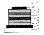
- the first gist of the present invention is an organic electroluminescence device having an anode, a light emitting layer, two or more electron transport layers and a cathode in this order, and at least one of the two or more electron transport layers is
- the light emitting layer is adjacent to the light emitting layer, the light emitting layer contains a light emitting material and a charge transport material, the electron transport layer adjacent to the light emitting layer contains a charge transport material, and the charge contained in the light emitting layer
- the charge transport material contained in the transport material and the electron transport layer adjacent to the light emitting layer may be the same material or different materials, and the charge transport material contained in the light emitting layer Among them, the electron affinity of the charge transport material responsible for electron transport is EA1, and among the charge transport materials contained in the electron transport layer adjacent to the light emitting layer, the electron of the charge transport material having the largest absolute value of electron affinity.
- EA1 and EA2 A charge that satisfies the relationship represented by the following formula (1) and has the largest absolute value of electron affinity among the charge transport materials contained in the electron transport layer closest to the cathode among the two or more electron transport layers.
- the organic electroluminescent element is characterized in that EA3 and WF satisfy the relationship represented by the following formula (2), where EA3 is the electron affinity of the transport material and WF is the work function of the cathode.
- the second gist of the present invention resides in an organic electroluminescent element characterized in that, in the first gist, the EA1 and the EA2 satisfy a relationship represented by the following formula (3).
- the third gist of the present invention resides in an organic electroluminescent element characterized in that, in the first or second gist, the EA3 and the WF satisfy a relationship represented by the following formula (4).
- a fourth aspect of the present invention is the charge transporting according to any one of the first to third aspects, wherein the electron transporting layer adjacent to the light emitting layer is different from the charge transporting material contained in the light emitting layer.
- the present invention resides in an organic electroluminescent device characterized by containing a material.
- the organic electroluminescent device according to any one of the first to fourth aspects wherein the light emitting layer is a layer produced by a wet film forming method.
- a sixth aspect of the present invention is an organic electroluminescent device having two or more types of organic electroluminescent elements that emit light of different colors on a substrate, and at least one organic type of the organic electroluminescent elements is provided.
- An organic electroluminescent device is characterized in that the electroluminescent device is the organic electroluminescent device according to any one of the first to fifth aspects.
- all the organic electroluminescent elements of the organic electroluminescent element are the organic electroluminescent elements according to any one of the first to fifth aspects. It exists in an organic electroluminescent device.
- the electron transport layer adjacent to the light emitting layer of at least two kinds of organic electroluminescent elements is the same. It exists in the organic electroluminescent device characterized by this.
- an organic EL display device comprising the organic electroluminescent element according to any one of the first to fifth aspects.
- a tenth aspect of the present invention resides in an organic EL illumination characterized by including the organic electroluminescent element described in any one of the first to fifth aspects.
- an organic electroluminescent device having a long lifetime and high luminous efficiency is provided. Since the organic electroluminescence device of the present invention has high current efficiency and a long driving life, a light source (for example, a flat panel display (for example, for office automation (OA) computers or wall-mounted televisions)) or a surface light emitter (for example) It can be applied to light sources for copying machines, backlight sources for liquid crystal displays and instruments), display panels, and marker lamps, and its technical value is high.
- a light source for example, a flat panel display (for example, for office automation (OA) computers or wall-mounted televisions)
- a surface light emitter for example
- the organic electroluminescent device of the present invention is an organic electroluminescent device having at least an anode, a luminescent layer, two or more electron transport layers and a cathode in this order, and at least one layer of the electron transport layer is adjacent to the luminescent layer.
- the light-emitting layer contains a light-emitting material and a charge transport material
- the electron transport layer adjacent to the light-emitting layer contains a charge transport material
- the charge transport material contained in the light-emitting layer and the light emission may be the same material or different materials, and among the charge transport materials contained in the light emitting layer,
- the electron affinity of the charge transporting material is EA1
- the electron affinity of the charge transporting material having the largest absolute value of the electron affinity is EA2.
- EA1 and EA2 The electron affinity of the charge transport material that satisfies the relationship represented by the following formula (1) and has the largest absolute value of the electron affinity among the charge transport materials contained in the electron transport layer on the cathode side of the electron transport layer.
- EA3 is EA3 and the work function of the cathode is WF
- EA3 and WF satisfy the relationship represented by the following formula (2).
- Formula (1) 0.00 eV ⁇
- the electron affinity may be abbreviated as “EA”.
- the organic electroluminescent element of the present invention has two or more electron transport layers.
- the electron transport layer refers to a dielectric layer having an electron transport property.
- the electron transport layer is formed of a compound capable of efficiently transporting electrons injected from the cathode between the electrodes to which an electric field is applied in the direction of the light emitting layer.
- the electron transport layer adjacent to the light emitting layer may be simply referred to as “adjacent electron transport layer”, and the most cathode side electron transport layer may be simply referred to as “cathode side electron transport layer”. is there.
- the electron injection layer refers to a non-conductive layer having an electron injection property from the cathode to the electron transport layer, and refers to a layer different from the electron transport layer according to the present invention.
- a cathode means the electrode which becomes a counter electrode of an anode.
- Charge transport material responsible for electron transport means that, when the light emitting layer contains two or more types of charge transport materials, the charge mobility measured by the Time of Flight (ToF) method of the single layer film of the charge transport material. Observed material having the highest ratio “Q (e) / Q (h)” of charge detection amount Q (e) at the time of electron mobility measurement to charge detection amount Q (h) at the time of hole mobility measurement Say that.
- the charge detection amount ratio “Q (e) / Q (h)” in charge mobility measurement by the ToF method can be measured by the following method.
- a sample for measurement is prepared by forming a charge transport material and a counter electrode to be measured on a semi-transparent electrode and then sealing.
- the charge transport material may be formed by either a wet method or a dry method as long as a good amorphous film is obtained.
- the film thickness of the charge transport film material to be formed the distance from the place where charge separation occurs at the time of charge transfer measurement to the counter electrode is sufficiently long, and the distance should not affect the evaluation of the charge transport property.
- the electric field strength is preferably 90 kV / cm or more, more preferably 120 kV / cm or more, and on the other hand, preferably 360 kV / cm or less, and 310 kV / cm or less. More preferably.
- the measurement sample is irradiated with a monochromatic light pulse laser from the translucent electrode side.
- the electric field intensity at the time of laser light irradiation, the excitation wavelength of the laser light, the pulse width, and the amount of light per pulse are determined based on the charge amount Q (h) of holes and the charge of electrons for the sample whose charge detection amount ratio is to be measured.
- the same conditions are used when measuring the quantity Q (e).
- the amount of light per pulse is preferably small in view of the low possibility that charge transportability is highly estimated due to the influence of an excessive amount of charge, and specifically, it is preferably 30 ⁇ J or less.
- the film of the charge transport material When the film of the charge transport material is irradiated with light, charge separation occurs on the translucent electrode side of the film, and holes move to the counter electrode side. By measuring this current value using an oscilloscope or the like, the hole charge amount Q (h) is calculated. Next, the electron charge amount Q (e) is calculated by applying a certain electric field strength so that the translucent electrode becomes the cathode and the counter electrode becomes the anode, and the same operation is performed. Then, by obtaining the ratio between the two, the charge detection amount ratio “Q (e) / Q (h)” can be obtained.
- the charge detection amount ratio “Q (e) / Q (h)” is an index indicating which of holes and electrons is more likely to flow. That is, as the charge detection amount ratio “Q (e) / Q (h)” is larger, the material is more likely to flow electrons.
- the hole mobility is measured in the charge mobility measured by the ToF method of the single layer film of the charge transport material when the light emitting layer according to the present invention includes a plurality of types of charge transport materials. It can be determined that the material having the largest ratio Q (e) / Q (h) between the charge detection amount and the charge detection amount at the time of measuring the electron mobility is the material responsible for electron transport.
- the work function of the cathode material can generally be obtained by photoelectron spectroscopy. Measurements using photoelectron spectroscopy are performed in an ultra-vacuum of 10 ⁇ 8 torr to 10 ⁇ 10 torr by irradiating the sample with ultraviolet monochromatic light or X-rays, and using electrons such as photomultiplier tubes. It can be determined by detecting and correlating the energy that excited the sample with the number of detected electrons. In particular, for the work function of a single material, see Michaelis, Hrbert B. et al. In 1977 (J. Appl. Phys., 48.4729 (1977)). Specifically, the case of aluminum will be described as an example.
- a clean amorphous aluminum thin film is produced by vapor-depositing aluminum on quartz which is a pedestal for measurement at a vacuum degree of 10 ⁇ 9 to 10 ⁇ 10 torr. Then, under ultra-vacuum, using a high-pressure mercury lamp as a light source, monochromatic light is taken out by a monochromator and irradiated on the sample surface. A value of 4.28 eV is calculated by calculating the number of electrons jumping out from the sample surface and taking a correlation with the energy of the light source.
- values such as 4.26 eV for silver, 5.10 eV for gold, and 5.15 eV for nickel are known as extremely general values. It has been.
- of the charge transport material responsible for electron transport among the charge transport materials in the light emitting layer is equal to that of the charge transport material in the adjacent electron transport layer.
- the charge transport material having the largest absolute value of EA is characterized by having an absolute value of EA of
- the accumulated electrons cause hole accumulation on the interface light emitting layer side between the light emitting layer and the adjacent electron transport layer, generation of exciplex at the interface, and the like.
- the generated charge may cause deterioration of the light emitting material and charge transporting material near the interface, leading to a reduction in device lifetime, and further inhibiting the generation of excitons in the light emitting layer and causing quenching of excitons.
- the light emitted from the light emitting layer near the interface cannot be extracted efficiently.
- the organic electroluminescence device of the present invention has an absolute value of the work function (WF) of the cathode and a charge transport material EA (AE) having the largest absolute value of the electron affinity among the charge transport materials in the cathode-side electron transport layer.
- the difference between the absolute value of EA3) is a certain value or less.
- the ionization potential (IP) of the charge transport material is a commercially available ionization potential measuring device such as “AC-1”, “AC-3” manufactured by Riken Keiki Co., Ltd., “PCR-101”, “PCR-201” manufactured by Optel. It can measure by using.
- a sample for measuring the ionization potential (IP) can be produced by depositing the charge transport material on the ITO substrate by a wet or dry method.
- the wet film forming method include a method in which the charge transporting material is dissolved in an organic solvent such as xylene or toluene and the film is formed by a spin coating method.
- the dry film forming method include a vacuum deposition method.
- Eg when the wavelength of the intersection is 470 nm is 1240 ⁇ 470 2.63 (eV).
- the energy indicating the band gap may be measured with an apparatus capable of measuring an absorption spectrum, and the type of the apparatus is not particularly limited.
- “F4500” manufactured by Hitachi, Ltd. can be used.
- a sample for measuring energy indicating a band gap can be produced by depositing the charge transport material on a glass substrate by a wet or dry method.
- the wet film forming method include a method in which the charge transporting material is dissolved in an organic solvent such as xylene or toluene and the film is formed by a spin coating method.
- the dry film forming method include a vacuum deposition method.
- the light emitting layer included in the organic electroluminescent element of the present invention includes at least one light emitting material (material having a light emitting property) and one or more charge transport materials.
- the light emitting layer may include a light emitting material as a dopant material and a charge transport material such as a hole transport material or an electron transport material as a host material.
- the light emitting layer may contain other components as long as the effects of the present invention are not significantly impaired.
- the light-emitting material any known material that is usually used as a light-emitting material of an organic electroluminescent element can be applied, and there is no particular limitation. Light is emitted at a desired light emission wavelength, and the light emission efficiency is good. A substance may be used.
- the light-emitting material may be a fluorescent light-emitting material or a phosphorescent light-emitting material, but is preferably a phosphorescent light-emitting material from the viewpoint of internal quantum efficiency. Further, for example, a fluorescent material and a phosphorescent material may be used in combination such that a fluorescent material is used for blue and a phosphorescent material is used for green and red.
- the symmetry and rigidity of the molecules of the light emitting material are reduced.
- fluorescent light emitting materials blue fluorescent dyes
- examples of fluorescent light emitting materials that emit blue light include naphthalene, chrysene, perylene, pyrene, anthracene, coumarin, p-bis (2-phenylethenyl) benzene, arylamine, and derivatives thereof. It is done. Among these, anthracene, chrysene, pyrene, arylamine and derivatives thereof are preferable.
- fluorescent light emitting material green fluorescent dye
- examples of the fluorescent light emitting material (green fluorescent dye) that gives green light emission include aluminum complexes such as quinacridone, coumarin, Al (C 9 H 6 NO) 3, and derivatives thereof.
- Examples of the fluorescent material that gives yellow light include rubrene, perimidone and derivatives thereof.
- fluorescent light emitting materials examples include DCM (4- (dicyanomethylene) -2-methyl-6- (p-dimethylaminostyrene) -4H-pyran) -based compounds, benzopyran, rhodamine , Xanthene such as benzothioxanthene, azabenzothioxanthene, and derivatives thereof.
- arylamine derivative which is a material that gives blue fluorescence
- a compound represented by the following formula (X) is preferable from the viewpoint of the light emission efficiency of the device, the driving life, and the like.
- Ar 21 represents a substituted or unsubstituted condensed aromatic ring group having 10 to 40 nuclear carbon atoms
- Ar 22 and Ar 23 each independently represents a substituted or unsubstituted monovalent group having 6 to 40 carbon atoms.
- p represents an integer of 1 to 4.
- the aromatic ring group in the present invention may be an aromatic hydrocarbon ring group or an aromatic heterocyclic group.
- Ar 21 examples include naphthalene, phenanthrene, fluoranthene, anthracene, pyrene, perylene, coronene, chrysene, picene, diphenylanthracene, fluorene, triphenylene, rubicene, benzoanthracene, phenylanthracene having one free valence. , Bisanthracene, dianthracenylbenzene, dibenzoanthracene and the like.
- free valence can form bonds with other free valences as described in Organic Chemistry / Biochemical Nomenclature (above) (Revised 2nd edition, Nankodo, 1992). Say things.
- a phosphorescent material for example, a long-period type periodic table (hereinafter, unless otherwise specified, the term “periodic table” refers to a long-period type periodic table) selected from Group 7 to 11 Wellner type complexes or organometallic complexes containing the above metal as the central metal.
- Preferred examples of the metal selected from Groups 7 to 11 of the periodic table include ruthenium, rhodium, palladium, silver, rhenium, osmium, iridium, platinum, gold, and the like. Among these, iridium or platinum is more preferable.
- a ligand in which a (hetero) aryl group such as a (hetero) arylpyridine ligand or a (hetero) arylpyrazole ligand and a pyridine, pyrazole, phenanthroline, or the like is connected is preferable.
- a pyridine ligand and a phenylpyrazole ligand are preferable.
- (hetero) aryl represents an aryl group or a heteroaryl group.
- phosphorescent materials include tris (2-phenylpyridine) iridium, tris (2-phenylpyridine) ruthenium, tris (2-phenylpyridine) palladium, bis (2-phenylpyridine) platinum, tris (2- Phenylpyridine) osmium, tris (2-phenylpyridine) rhenium, octaethylplatinum porphyrin, octaphenylplatinum porphyrin, octaethyl palladium porphyrin, octaphenyl palladium porphyrin, and the like.
- the phosphorescent organometallic complex of the phosphorescent material is preferably a compound represented by the following formula (III) or formula (IV).
- M represents a metal
- q represents a valence of the metal
- L and L ′ represent a bidentate ligand
- j represents a number of 0, 1 or 2.
- M 7 represents a metal
- T represents a carbon atom or a nitrogen atom.
- R 92 to R 95 each independently represents a substituent. However, when T is a nitrogen atom, R 7 No 94 and R 95 )
- M represents an arbitrary metal, and specific examples of preferable ones include the metals described above as metals selected from Groups 7 to 11 of the periodic table.
- bidentate ligand L represents a ligand having the following partial structure.
- ring A1 represents an aromatic ring group which may have a substituent.
- the aromatic ring group in the present invention may be an aromatic hydrocarbon ring group or an aromatic heterocyclic group.
- aromatic hydrocarbon ring group examples include a 5- or 6-membered monocyclic ring or a 2-5 condensed ring having one free valence.
- Specific examples of the aromatic hydrocarbon ring group include a benzene ring, naphthalene ring, anthracene ring, phenanthrene ring, perylene ring, tetracene ring, pyrene ring, benzpyrene ring, chrysene ring, triphenylene having one free valence. Ring, acenaphthene ring, fluoranthene ring, fluorene ring and the like.
- aromatic heterocyclic group examples include a 5- or 6-membered monocyclic ring or a 2-4 condensed ring having one free valence.
- Specific examples include a furan ring, benzofuran ring, thiophene ring, benzothiophene ring, pyrrole ring, pyrazole ring, imidazole ring, oxadiazole ring, indole ring, carbazole ring, pyrroloimidazole ring having one free valence.
- ring A2 represents a nitrogen-containing aromatic heterocyclic group which may have a substituent.
- nitrogen-containing aromatic heterocyclic group examples include a 5- or 6-membered monocyclic ring or a 2-4 condensed ring having one free valence.
- Specific examples include a pyrrole ring, a pyrazole ring, an imidazole ring, an oxadiazole ring, an indole ring, a carbazole ring, a pyrroloimidazole ring, a pyrrolopyrazole ring, a pyrrolopyrrole ring, a thienopyrrole ring, and a fluropyrrole having one free valence.
- each of ring A1 and ring A2 may have include a halogen atom; an alkyl group; an alkenyl group; an alkoxycarbonyl group; an alkoxy group; an aryloxy group; a dialkylamino group; Acyl group; haloalkyl group; cyano group; aromatic hydrocarbon ring group and the like.
- ring A1 is a nitrogen-containing aromatic heterocyclic group and ring A2 may have an aromatic hydrocarbon ring group as a substituent.
- bidentate ligand L ′ represents a ligand having the following partial structure. However, in the following formulae, “Ph” represents a phenyl group.
- L ′ the following ligands are preferable from the viewpoint of stability of the complex.
- More preferable examples of the compound represented by the formula (III) include compounds represented by the following formulas (IIIa), (IIIb), and (IIIc).
- M 4 represents the same metal as M
- w represents the valence of the metal
- ring A1 represents an aromatic hydrocarbon ring group which may have a substituent.
- Ring A2 represents a nitrogen-containing aromatic heterocyclic group which may have a substituent.
- M 5 represents the same metal as M
- w represents the valence of the metal
- ring A 1 represents an aromatic ring group which may have a substituent
- ring A2 represents a nitrogen-containing aromatic heterocyclic group which may have a substituent.
- M 6 represents the same metal as M, w represents the valence of the metal, j represents 0, 1 or 2, and ring A1 and ring A1 ′ each represent Independently, it represents an aromatic ring group which may have a substituent, and ring A2 and ring A2 ′ each independently represent a nitrogen-containing aromatic heterocyclic group which may have a substituent.
- aromatic group of ring A1 and ring A1 ′ include phenyl group, biphenyl group, naphthyl group, anthryl group, thienyl group, furyl group, benzothienyl group, benzofuryl group.
- aromatic group of ring A1 and ring A1 ′ include phenyl group, biphenyl group, naphthyl group, anthryl group, thienyl group, furyl group, benzothienyl group, benzofuryl group.
- preferred examples of the nitrogen-containing aromatic heterocyclic group for ring A2 and ring A2 ′ include pyridyl group, pyrimidyl group, pyrazyl group, triazyl group, benzothiazole group, benzoxazole group. Benzoimidazole group, quinolyl group, isoquinolyl group, quinoxalyl group, phenanthridyl group and the like.
- the aromatic ring group of ring A1 and ring A1 ′ and the nitrogen-containing aromatic heterocyclic group of ring A2 and ring A2 ′ may have a halogen atom; Alkyl group; alkenyl group; alkoxycarbonyl group; alkoxy group; aryloxy group; dialkylamino group; diarylamino group; carbazolyl group; acyl group; haloalkyl group; These substituents may be connected to each other to form a ring.
- a substituent of the ring A1 and a substituent of the ring A2 are bonded, or a substituent of the ring A1 ′ and a substituent of the ring A2 ′ are bonded.
- a condensed ring may be formed. Examples of such a condensed ring include a 7,8-benzoquinoline group.
- ring A1 ′, ring A2 and ring A2 ′ more preferably, an alkyl group, an alkoxy group, an aromatic hydrocarbon ring group, a cyano group, a halogen atom, a haloalkyl group, a diarylamino group, And a carbazolyl group.
- M 4 to M 6 in the formulas (IIIa) to (IIIc) include ruthenium, rhodium, palladium, silver, rhenium, osmium, iridium, platinum or gold.
- organometallic complexes represented by the above formulas (III) and (IIIa) to (IIIc) are shown below, but are not limited to the following compounds.
- organometallic complexes represented by the above formula (III) in particular, as the ligand L and / or L ′, a 2-arylpyridine-based ligand, that is, 2-arylpyridine, which has an optional substituent.
- a 2-arylpyridine-based ligand that is, 2-arylpyridine, which has an optional substituent.
- bonded and what an arbitrary group condensed to this is preferable.
- M 7 represents a metal. Specific examples include the metals described above as the metal selected from Groups 7 to 11 of the periodic table. M 7 is preferably ruthenium, rhodium, palladium, silver, rhenium, osmium, iridium, platinum or gold, and particularly preferably a divalent metal such as platinum or palladium.
- R 92 and R 93 each independently represent a hydrogen atom, a halogen atom, an alkyl group, an aralkyl group, an alkenyl group, a cyano group, an amino group, an acyl group, an alkoxycarbonyl group, a carboxyl group, An alkoxy group, an alkylamino group, an aralkylamino group, a haloalkyl group, a hydroxyl group, an aryloxy group, and an aromatic ring group are represented.
- R 94 and R 95 each independently represent the same substituent as those listed as R 92 and R 93 .
- R 94 and R 95 are absent.
- R 92 to R 95 may further have a substituent.
- it has a substituent there is no restriction
- any two or more groups of R 92 to R 95 may be connected to each other to form a ring.
- T-1, T-10 to T-15 Specific examples (T-1, T-10 to T-15) of the organometallic complex represented by the formula (IV) are shown below, but are not limited to the following examples.
- “Me” represents a methyl group
- “Et” represents an ethyl group.
- These light emitting materials may be used alone, or two or more kinds may be used in any combination and ratio.
- the molecular weight of the luminescent material in the present invention is arbitrary as long as the effects of the present invention are not significantly impaired.
- the molecular weight of the luminescent material in the present invention is preferably 10,000 or less, more preferably 5000 or less, still more preferably 4000 or less, and particularly preferably 3000 or less.
- the molecular weight of the light emitting material in the present invention is usually 100 or more, preferably 200 or more, more preferably 300 or more, and still more preferably 400 or more.
- the molecular weight of the luminescent material is due to the high glass transition temperature, melting point, decomposition temperature, etc., excellent heat resistance of the luminescent layer material and the formed luminescent layer, and gas generation, recrystallization, and molecular migration. It is preferable that the film quality is low and the impurity concentration is not increased due to thermal decomposition of the material.
- the molecular weight of the light-emitting material is preferably small in that the organic compound can be easily purified and easily dissolved in a solvent.
- the light emitting layer according to the present invention preferably contains a light emitting material in an amount of usually 0.01% by weight or more, preferably 0.05% by weight or more, and more preferably 0.1% by weight or more. Further, the light emitting material is usually contained in an amount of 35% by weight or less, preferably 20% by weight or less, more preferably 10% by weight or less. In addition, when using together 2 or more types of luminescent material, it is preferable that these total content is included in the said range.
- the light emitting material preferably emits light by receiving charge or energy from a host material having charge transport performance.
- the emissive layer typically includes a charge transport material, such as that used for example as the host material.
- the charge transport material includes a compound having a hole transport property (sometimes referred to as a hole transport material or a hole transport compound) and a compound having an electron transport property (referred to as an electron transport material or an electron transport compound). There is).
- the light emitting layer may contain both a hole transport material and an electron transport material, or may contain either one.
- the light emitting layer contains the compound which has hole transportability, when the compound which has electron transportability is not included, the compound which has hole transportability should just transport an electron in a light emitting layer.
- examples of the charge transport material include aromatic amine compounds, phthalocyanine compounds, porphyrin compounds, thiophene compounds, benzylphenyl compounds, fluorene compounds, hydrazone compounds, silazane compounds, silanamine compounds, Phosphamine compounds, quinacridone compounds, triphenylene compounds, carbazole compounds, pyrene compounds, anthracene compounds, phenanthroline compounds, quinoline compounds, pyridine compounds, triazine compounds, oxadiazole compounds, imidazole compounds, etc. Is mentioned.
- the electron transport material is preferably a compound having an electron transporting unit.
- An electron transporting unit (electron transporting unit) is a structure (unit) having excellent durability against electrons and having electron transporting properties. Further, when two or more kinds of charge transport materials are included in the light emitting layer, the compound having this electron transport unit tends to be the charge transport material responsible for the electron transport described above.
- the electron transport unit in the present invention is a unit in which electrons easily enter the unit and stabilize the contained electrons.
- a pyridine ring or the like has a slight electron deficiency due to a nitrogen atom, easily accepts an electron, and the electron entering the ring is delocalized to be stabilized on the pyridine ring.
- Examples of the structure of the unit having the above performance include a single ring or a condensed ring containing a hetero atom composed of sp 2 hybrid orbitals.
- nitrogen, oxygen, sulfur, and selenium are preferable, and nitrogen is particularly preferable because the hetero atom easily forms sp 2 hybrid orbitals, has high stability to electrons, and high electron transport properties.
- the number of heteroatoms having sp 2 hybrid orbitals included in the charge transport material is preferably large in view of high electron transport properties.
- electron transport unit examples include quinoline ring, quinazoline ring, quinoxaline ring, phenanthroline ring, pyridine ring, pyrimidine ring, pyridazine ring, pyrazine ring, triazine ring, thiadiazole ring, benzothiadiazole ring, quinolinol metal complex, phenanthroline metal A complex, a hexaazatriphenylene structure, a tetrasiabenzoquinoline structure, and the like can be given.
- quinoline ring, quinazoline ring, quinoxaline ring, phenanthroline ring, pyridine ring, pyrimidine ring, pyridazine ring, pyrazine ring, triazine ring and the like are preferable.
- quinoline ring, quinazoline ring, pyridine ring, pyrimidine ring, triazine ring, 1,10-phenanthroline ring and the like are preferable from the viewpoint of excellent electrical stability.
- the electron transport unit is a 6-membered monocyclic ring or condensed ring containing a nitrogen atom
- the o-position and the p-position are all substituted with an aromatic ring with respect to the nitrogen atom. .
- the reason is as follows. That is, the o-position and p-position of a 6-membered ring containing a nitrogen atom are active sites, and electrons are delocalized by substitution with an aromatic ring group. This makes it more stable with electrons.
- the electron transport unit is a 6-membered condensed ring containing a nitrogen atom
- a portion of the o-position and p-position of the nitrogen atom that does not form part of the condensed ring is an aromatic ring. It only needs to be substituted with a group.
- an organic compound having a ring derivative listed in the following group (b) is more preferable because of its high stability against electrons and high electron transport properties.
- the aromatic ring group in which the hydrogen atoms on the carbon atoms at the 2, 4 and 6 positions in the same ring are substituted with respect to the nitrogen atom is not particularly limited. That is, it may be an aromatic hydrocarbon ring group or an aromatic heterocyclic group, but may be an aromatic hydrocarbon ring group in that it has excellent durability against electrical oxidation. preferable.
- the number of carbon atoms in the aromatic ring group is preferably 6 to 30, and when the aromatic ring group is a condensed ring, the number of condensed aromatic rings is preferably 2 to 4.
- substituents of the ring structure included in the group (b) include a halogen atom, an alkyl group having 1 to 10 carbon atoms which may further have a substituent, and 2 to 10 carbon atoms. Or a monovalent aromatic hydrocarbon ring group having 6 to 30 carbon atoms.
- 2,5-bis (1-naphthyl) -1,3,4-oxadiazole BND
- 2,5-bis (6 ′-(2 ′, 2 ′′-) Bipyridyl))-1,1-dimethyl-3,4-diphenylsilole PyPySPyPy
- bathophenanthroline BPhen
- 2,9-dimethyl-4,7-diphenyl-1,10-phenanthroline BCP, bathocuproin
- 2 -(4-biphenylyl) -5- (p-tertiarybutylphenyl) -1,3,4-oxadiazole tBu-PBD
- the hole transport material is preferably a compound having a hole transporting unit.
- the hole transporting unit (hole transporting unit) is a structure (unit) having excellent durability against holes and having hole transporting properties.
- the hole transport unit in the present invention means a unit that has an ionization potential that facilitates extraction of holes from the light emitting layer and is stable to holes.
- the ionization potential at which holes are easily extracted from the light emitting layer is usually 5.4 eV or more, preferably 5.5 eV or more, more preferably 5.6 eV or more, and usually 6.3 eV or less, preferably 6. 2 eV, more preferably 6.1 eV or less.
- being stable to holes means that the hole transport unit is not easily decomposed even in a radical state. This means that the radical cation is delocalized so that it is stabilized even in the radical state.
- Examples of the structure of the unit having the above-described performance include a structure containing a hetero atom having sp 3 orbital or a 4n-based aromatic condensed ring.
- hole transport unit examples include carbazole ring, phthalocyanine ring, naphthalocyanine structure, porphyrin structure, triarylamine structure, triarylphosphine structure, benzofuran ring, dibenzofuran ring, pyrene ring, phenylenediamine structure, pyrrole ring, Examples include a benzidine structure, an aniline structure, a diarylamine structure, an imidazolidinone structure, and a pyrazole ring.
- a carbazole ring, benzofuran ring, dibenzofuran ring, pyrene ring, triarylamine structure more preferably carbazole ring, benzofuran ring, A dibenzofuran ring and a pyrene ring are preferable, and a carbazole ring and a pyrene ring are particularly preferable.
- hole transport material an organic compound having a derivative of any of the rings listed in the following group (a) (hole transport unit) is more excellent because of excellent stability against holes and high hole transportability. preferable.
- These ring structures may have a substituent, and preferred substituents include a halogen atom, an alkyl group having 1 to 10 carbon atoms which may further have a substituent, and 2 to 2 carbon atoms. And an alkenyl group having 10 or a monovalent aromatic hydrocarbon ring group having 6 to 30 carbon atoms.
- a low molecular weight hole transport material two or more tertiary amines represented by 4,4′-bis [N- (1-naphthyl) -N-phenylamino] biphenyl And an aromatic amine compound in which two or more condensed aromatic rings are substituted with nitrogen atoms (Japanese Patent Laid-Open No. 5-234811), 4,4 ′, 4 ′′ -tris (1-naphthylphenylamino) tri Aromatic amine compounds having a starburst structure such as phenylamine (Journal of Luminescence, 1997, Vol. 72-74, pp.
- aromatic amine compounds consisting of tetramers of triphenylamine (Chemical Communications) , 1996, pp. 2175), 2,2 ′, 7,7′-tetrakis- (diphenylamino) -9,9 ′.
- -Fluorene compounds such as spirobifluorene (Synthetic Metals, 1997, Vol. 91, pp. 209), etc.
- a (low molecular weight hole transport material) in [Hole injection layer] described later The exemplified compounds can be used. In the light emitting layer, only one type of hole transport material may be used, or two or more types may be used in any combination and ratio.
- the molecular weight of the charge transport material in the present invention is arbitrary as long as the effects of the present invention are not significantly impaired.
- the molecular weight of the charge transport material in the present invention is usually 10,000 or less, preferably 5000 or less, more preferably 4000 or less, and still more preferably 3000 or less.
- the molecular weight of the charge transport material in the present invention is usually 100 or more, preferably 200 or more, more preferably 300 or more, and still more preferably 400 or more.
- the glass transition temperature, melting point, decomposition temperature, etc. are high, the heat resistance of the light emitting layer material and the formed light emitting layer is good, and recrystallization and molecular It is preferable in that the film quality is reduced due to the migration of the material, the impurity concentration is not increased due to thermal decomposition of the material, the device performance is excellent, and the purification is easy.
- the light emitting layer may contain only one kind of charge transport material as described above, or may contain two or more kinds.
- the charge transport material (electron transport) mainly responsible for electron transport is compared with the EA of charge transport material (hole transport material) mainly responsible for transport of holes. It is desirable that the EA of the material is larger. That is, in general, when a plurality of charge transport materials are included in the same layer, electrons are likely to ride on a material having a large EA. Therefore, by using a charge transport material having a large EA as an electron transport material, high luminous efficiency / It is possible to produce a long-life element.
- of the charge transport material responsible for electron transport contained in the light emitting layer according to the present invention is large in that the compound is likely to be in a stable state when electrons exist in the energy level for transporting electrons. However, on the other hand, it is preferably small from the standpoint that transport and transfer of charges due to formation of a stable radical anion and inhibition of exciton formation are unlikely to occur.
- is preferably 2.40 eV or more, more preferably 2.50 eV, and on the other hand, it is preferably 3.30 eV or less, and 3.20 eV or less. Preferably there is.
- the following tendencies are often recognized between the chemical structure of the charge transport material and
- the light emitting layer according to the present invention preferably contains a charge transport material in an amount of usually 65% by weight or more, preferably 80% by weight or more, and more preferably 90% by weight or more. Further, the charge transport material is usually contained in 99.99% by weight or less, preferably 99.95% by weight or less, more preferably 99.9% by weight or less. In addition, when using together 2 or more types of charge transport materials, it is preferable that these total content is included in the said range.
- the light emitting layer according to the present invention has a high material utilization efficiency, and the hole injection layer is easily mixed with the hole transport layer formed on the anode side, so that the hole injection property is likely to be good. Is preferably formed.
- the wet film forming method is a film forming method, that is, a coating method, for example, spin coating method, dip coating method, die coating method, bar coating method, blade coating method, roll coating method, spray coating method, capillary A method of forming a film by employing a wet film formation method such as a coating method, an ink jet method, a nozzle printing method, a screen printing method, a gravure printing method, or a flexographic printing method, and drying the coated film.
- a spin coating method, a spray coating method, an ink jet method, and a nozzle printing method are preferable.
- a light emitting layer When forming a light emitting layer by a wet film-forming method, usually a light emitting layer formed by dissolving the above-described light emitting material, charge transporting material, and other materials described later used as necessary in an appropriate solvent. It forms by forming into a film using the composition for water.
- the solvent used in the wet film forming method of the light emitting layer is not particularly limited as long as the material used for forming the light emitting layer such as the light emitting material and the charge transporting material can be dissolved or dispersed well.
- the light emitting material and the charge transport material are each usually 0.01% by weight or more, preferably 0.05% by weight or more, more preferably 0.1% by weight at 25 ° C. and 1 atm. It is preferable to dissolve the above.
- the solvent examples include alkanes such as n-decane, cyclohexane, ethylcyclohexane, decalin and bicyclohexane; aromatic hydrocarbons such as toluene, xylene, methicylene, cyclohexylbenzene, tetramethylcyclohexanone and tetralin; chlorobenzene and dichlorobenzene Halogenated aromatic hydrocarbons such as trichlorobenzene; 1,2-dimethoxybenzene, 1,3-dimethoxybenzene, anisole, phenetole, 2-methoxytoluene, 3-methoxytoluene, 4-methoxytoluene, 2,3- Aromatic ethers such as dimethylanisole, 2,4-dimethylanisole, diphenyl ether; phenyl acetate, phenyl propionate, methyl benzoate, ethyl benzoate, e
- solvents may be used alone, or two or more may be used in any combination and ratio.
- the solvent evaporates from the liquid film immediately after the film formation at an appropriate rate.
- the boiling point of the solvent is usually 80 ° C. or higher, preferably 100 ° C. or higher, more preferably 120 ° C. or higher.
- the boiling point of the solvent is usually 270 ° C. or lower, preferably 250 ° C. or lower, more preferably 230 ° C. or lower.
- composition for forming a light emitting layer in the present invention preferably contains a light emitting material in an amount of usually 0.01% by weight or more, preferably 0.05% by weight or more, more preferably 0.1% by weight or more. Further, the light emitting material is usually contained in an amount of 20% by weight or less, preferably 10% by weight or less, more preferably 5% by weight or less.
- the composition for forming a light emitting layer in the present invention preferably contains a charge transport material in an amount of usually 0.1% by weight or more, preferably 0.5% by weight or more, and more preferably 1% by weight or more.
- the ratio of the content of the light emitting material and the charge transport material in the composition for forming the light emitting layer is usually 0.01 or more, preferably 0.03 or more. Is good.
- the ratio of the content of the light emitting material and the charge transport material in the composition for forming the light emitting layer is usually 0.5 or less, preferably 0.2 or less. Is good.
- the content of the solvent in the composition for forming a light emitting layer according to the present invention is arbitrary as long as the effects of the present invention are not significantly impaired.
- the content of the solvent in the composition for forming a light emitting layer is large, it is preferable from the viewpoint of low viscosity and excellent workability in film formation.
- the content of the solvent is small, it is preferable in that the thickness of a film obtained by removing the solvent after film formation can be easily obtained and film formation is easy.
- the content of the solvent is preferably 10 parts by weight or more, more preferably 50 parts by weight or more, and particularly preferably 80 parts by weight or more with respect to 100 parts by weight of the composition for forming a light emitting layer. good.
- the content of the solvent is preferably 99.95 parts by weight or less, more preferably 99.9 parts by weight or less, and particularly preferably 99.8 parts by weight or less.
- the composition for forming a light emitting layer in the present invention may contain various additives such as a leveling agent and an antifoaming agent for the purpose of improving the film formability.
- the solid content concentration which is the total amount of the light emitting material, hole transport material, electron transport material, and the like in the composition for forming a light emitting layer in the present invention, is preferably small in that film thickness unevenness is unlikely to occur. In view of the fact that defects are unlikely to occur in the film, it is preferable that the number be large. Specifically, it is preferably 0.01% by weight or more and usually 70% by weight or less.
- the formation of the light-emitting layer was usually obtained after such a composition for forming a light-emitting layer was wet-formed on a layer (usually a hole injection layer or a hole transport layer described later) as a lower layer of the light-emitting layer. It is formed by drying the coating film and removing the solvent.
- the thickness of the light emitting layer is arbitrary as long as the effects of the present invention are not significantly impaired. However, it is preferable that the film is thick in that it is difficult to cause defects in the film, but on the other hand, it is thin in that the driving voltage tends to be low. preferable. Specifically, the thickness is usually 3 nm or more, preferably 5 nm or more, and usually 200 nm or less, preferably 100 nm or less.
- the organic electroluminescent element may be provided with two or more light emitting layers.
- the number of light emitting layers is two or more, the conditions of each layer are as described above, but the definition of EA with the adjacent electron transport layer only needs to satisfy the light emitting layer having the electron transport layer adjacent to the cathode side. .
- the adjacent electron transport layer is a dielectric layer having an electron transport property provided between the light emitting layer and the cathode and adjacent to the light emitting layer.
- the adjacent electron transport layer is an electron transport property that transports electrons injected from the cathode to the light emitting layer, and a hole blocking property that prevents holes transported to the light emitting layer from leaking to the cathode side, or a light emitting layer. It is preferable to have a hole relaxation property that prevents the generated excitons from diffusing.
- limiting in the formation method of an adjacent electron carrying layer Therefore, it can be formed by a wet film forming method, a vapor deposition method, or other methods.
- the film thickness of the adjacent electron transport layer is arbitrary as long as the effect of the present invention is not significantly impaired, but is usually 0.3 nm or more, preferably 0.5 nm or more, and usually 100 nm or less, preferably 50 nm or less.
- the charge transport material for forming the adjacent electron transport layer is preferably electron transport.
- Organic compounds having a functional unit and a hole transporting unit are used.
- the hole transport unit is excellent in durability against holes and has a structure having a hole transport property.
- the electron transport unit is excellent in durability against electrons and has a structure having electron transport properties. That is, the adjacent electron transport layer according to the present invention preferably contains a charge transport material having excellent durability against electrical redox.
- the number of hole transport units and electron transport units included in the charge transport material contained in the adjacent electron transport layer is not limited as long as the charge transport material has hole transport properties and electron transport properties. It is preferable that the amount is high in terms of high properties, and on the other hand, it is preferable that it is small in terms of ease of purification. Specifically, it is preferably 1 or more for each of the hole transport unit and the electron transport unit, and on the other hand, it is preferably 10 or less, and more preferably 5 or less.
- the ratio of the number of hole transport units and electron transport units may be the same or one unit may be larger than the other unit, but the number of electron transport units is greater than the number of hole transport units. It is preferable to do this.
- the difference is preferably 1 or more, and on the other hand, it is preferably 5 or less, and more preferably 3 or less. preferable.
- the structure and preferred specific examples of the hole transport unit and the electron transport unit are as described above.
- the hole transport unit and the electron transport unit may be combined in any way as long as each unit exhibits a hole transport property and an electron transport property. Specifically, both units may be directly bonded, or a bonding group may be interposed between both units.
- a bonding group via the hole transport unit and the electron transport unit an alkylene group which may have a substituent, an alkenylene group which may have a substituent, and a divalent which may have a substituent Aromatic hydrocarbon ring groups are preferred.
- the carbon number of the alkylene group is preferably 1 or more, and on the other hand, it is preferably 10 or less, and more preferably 8 or less.
- Specific examples include a methylene group, 1,2-ethylene group, 1,3-propylene group, 1,4-butylene group, 1,5-pentylene group, 1,8-octylene group, and the like. Of these, a methylene group and a 1,2-ethylene group, which are easy to synthesize, are preferred.
- the carbon number of the alkenylene group is preferably 2 or more, on the other hand, preferably 10 or less, and more preferably 6 or less.
- Specific examples include 1,2-vinylene group, 1,3-propenylene group, 1,2-propenylene group, 1,4-butenylene group, etc.
- the conjugate plane is expanded by improving the planarity of the molecule.
- a vinylene group is preferable because the charge is delocalized and stability is easily improved.
- the carbon number of the divalent aromatic hydrocarbon ring group is preferably 6 or more, and on the other hand, it is preferably 30 or less.
- the number of condensed rings is preferably 5 or less. That is, a monocyclic ring, a 2-5 condensed ring, or a divalent group formed by connecting a plurality of these rings is preferable.
- the number is preferably 2 to 8 and more preferably 2 to 5 in view of high stability of the ring.
- the divalent aromatic hydrocarbon ring group examples include a benzene ring having a divalent free valence, a naphthalene ring, a phenanthrene ring, an anthracene ring, a triphenylene ring, a chrysene ring, a naphthacene ring, a perylene ring, and a coronene ring.
- a benzene ring, a naphthalene ring, an anthracene ring, a triphenylene ring and the like having a divalent free valence are preferable from the viewpoint of high ring stability.
- divalent aromatic hydrocarbon ring group is represented by structural formulas S1 to S15 below, but the present invention is not limited thereto.
- the bonding group may or may not have a substituent.
- the bonding group is not substituted in that the stability of the film is likely to be improved due to the decrease in crystallinity of the molecule due to the improvement in stability to electrons.
- an alkyl group When the linking group has a substituent, an alkyl group, an aromatic hydrocarbon ring group, an aromatic heterocyclic group, an alkoxy group, a (hetero) aryloxy group, an alkylthio group, a (hetero) arylthio group, a cyano group and the like are preferable (
- “(hetero) aryl” means both “aryl” and “heteroaryl”.
- an alkyl group is preferable in terms of the stability of the compound.
- the term “having an alkyl group as a substituent” means that the linking group is a group other than an alkylene group, and the term “having an aromatic hydrocarbon ring group as a substituent means that the linking group is an aromatic hydrocarbon”. This refers to a group other than a cyclic group.
- the carbon number of the alkyl group is preferably 1 or more, and on the other hand, it is preferably 20 or less.
- Specific examples include methyl group, ethyl group, propyl group, isopropyl group, butyl group, iso-butyl group, sec-butyl group, tert-butyl group, hexyl group, octyl group, cyclohexyl group, decyl group and octadecyl group.
- a methyl group, an ethyl group, and an isopropyl group are preferable, and a methyl group and an ethyl group are particularly preferable because the raw materials are easily available and can be easily synthesized at low cost.
- the number of carbon atoms of the aromatic hydrocarbon ring group of the substituent is preferably 6 or more, and is preferably 25 or less.
- Specific examples of the aromatic hydrocarbon ring group as a substituent include naphthyl groups such as phenyl group, 1-naphthyl group and 2-naphthyl group; phenanthyl groups such as 9-phenanthyl group and 3-phenanthyl group, 1-anthryl.
- anthryl groups such as 2-anthryl group and 9-anthryl group
- naphthacenyl groups such as 1-naphthacenyl group and 2-naphthacenyl group
- pyrenyl groups such as 1-pyrenyl groups, triphenylenyl groups such as 1-triphenylenyl groups and coronenyl groups such as 1-coronenyl groups, 4-biphenyl groups, 3-biphenyl groups And the like.
- a phenyl group, a 2-naphthyl group, a 3-biphenyl group, and the like are preferable from the viewpoint of stability of the compound, and a phenyl group is particularly preferable from the viewpoint of ease of purification.
- the number of carbon atoms of the aromatic heterocyclic group of the substituent is preferably 3 or more, and preferably 20 or less.
- Specific examples of the aromatic hydrocarbon ring group as a substituent include a thienyl group such as a 2-thienyl group; a furyl group such as a 2-furyl group; an imidazolyl group such as a 2-imidazolyl group; and a carbazolyl such as a 9-carbazolyl group.
- Groups; pyridyl groups such as 2-pyridyl group and triazinyl groups such as 1,3,5-triazin-2-yl group and the like.
- the alkoxy group preferably has 1 or more carbon atoms, and preferably 20 or less. Specific examples include methoxy group, ethoxy group, isopropyloxy group, cyclohexyloxy group, octadecyloxy group and the like.
- the (hetero) aryloxy group preferably has 3 or more carbon atoms, and preferably 20 or less. Specific examples include phenoxy group, 1-naphthyloxy group, 9-anthranyloxy group, 2-thienyloxy group and the like.
- the alkylthio group preferably has 1 or more carbon atoms, and preferably 20 or less. Specific examples include methylthio group, ethylthio group, isopropylthio group, cyclohexylthio group and the like.
- the (hetero) arylthio group preferably has 3 or more carbon atoms, and preferably 20 or less. Specific examples include phenylthio group, 1-naphthylthio group, 9-anthranylthio group, 2-thienylthio group and the like.
- the charge transport material contained in the adjacent electron transport layer for example, compounds having structures represented by the following general formulas (5) to (7) are preferable.
- A represents a hole transport unit having 1 to 30 carbon atoms which may have a substituent
- B represents an electron transport unit having 1 to 30 carbon atoms which may have a substituent
- L represents an optionally substituted hydrocarbon group having 1 to 30 carbon atoms
- l represents an integer of 0 to 3
- m and n each represents an integer of 1 to 4.
- a plurality of L, A, and B may be the same or different, and x and y represent an integer of 1 to 4, and x or y is 2 In the case of the above integers, a plurality of LA and LB may be the same or different.
- A represents a monovalent group
- a in the general formula (7) represents a y-valent group.
- B in the general formulas (5) and (7) both represents a monovalent group
- B in the general formula (6) represents an x-valent group.
- (L) l in the general formula (5) represents an m + n valent group
- L in the general formulas (6) to (7) represents a divalent group.
- A is preferably the above-described hole transport unit
- B is preferably the above-described electron transport unit B
- L is preferably the above-described bonding group.
- L is an optionally substituted saturated hydrocarbon group having 1 to 10 carbon atoms, an unsaturated hydrocarbon group having 2 to 10 carbon atoms, or an aromatic hydrocarbon ring group having 6 to 30 carbon atoms. It is particularly preferred.
- the structures of the formulas (5) to (7) are specifically expressed by the formula (5) when l, m, and n are 1, when the formula (6) is x, and when the formula (7) is y When “1” is 1, both are “ALB”. Further, the formulas (5) to (7) each have a structure such as the following formulas (5 ′) to (7 ′), for example.
- the molecular weight of the organic compound used as the charge transport material for forming the adjacent electron transport layer is preferably in the following range in terms of good heat resistance, hardly causing gas generation, easy purification, and high purity. That is, it is usually 10,000 or less, preferably 5000 or less, more preferably 4000 or less, further preferably 3000 or less, and usually 100 or more, preferably 200 or more, more preferably 300 or more, and further preferably 400 or more. Is good.
- the adjacent electron transport layer may contain only one kind of the charge transport material as described above, or may contain two or more kinds.
- the charge transport material (electron) mainly responsible for electron transport is compared with EA of the charge transport material (hole transport material) mainly responsible for transport of holes. It is desirable that the EA of the transport material is larger. That is, in general, when a plurality of charge transport materials are included in the same layer, electrons are likely to ride on a material having a large EA. Therefore, by using a charge transport material having a large EA as an electron transport material, high luminous efficiency / It is possible to produce a long-life element.
- of the EA of the charge transport material contained in the adjacent electron transport layer according to the present invention is large in that the compound tends to be in a stable state when electrons are present at the energy level for transporting electrons.
- it is preferably small from the standpoint that transport and transfer of charges due to formation of a stable radical anion and inhibition of exciton formation are unlikely to occur.
- the EA of the charge transport material having the largest absolute value of EA (if the adjacent electron transport layer contains only one type of charge transport material, the charge transport material
- the organic electroluminescent device of the present invention is the most absolute of the charge transport materials contained in the light emitting layer, the electron affinity EA1 of the charge transport material responsible for electron transport, and the charge transport material contained in the adjacent electron transport layer.
- the charge affinity material EA2 of the charge transport material having a large electron affinity satisfies the relationship represented by the following formula (1), preferably the following formula (3).
- is 0.00 eV or more, preferably 0.01 eV or more, particularly preferably 0. 0.04 eV or more is preferable.
- is 0.20 eV or less, preferably 0.19 eV or less, more preferably 0.17 eV or less.
- the charge transport material contained in the light emitting layer and the charge transport material contained in the adjacent electron transport layer may be the same or different materials, but the adjacent electron transport layer is the light emitting layer. It is preferable that a charge transporting material different from the charge transporting material contained in is contained. This is because the charge transport material contained in the light-emitting layer is required to have a characteristic that allows the light-emitting material to emit light efficiently, whereas the adjacent electron transport layer generally has efficient electron transport and hole blocking or relaxation. This is because the required material properties are different.
- the charge transport materials having the largest EA among the layers are different materials.
- the electron transport is mainly performed by the charge transport material having the largest EA in each layer.
- the optimum material is naturally different. to cause.
- the combination of the charge transport materials is temporarily selected, the EA is measured for each charge transport material according to the method described above, and the light emitting layer
- the charge transport material used for the light-emitting layer and the adjacent electron transport layer are used so that the charge transport material used for and the charge transport material used for the adjacent electron transport layer satisfy the relationship of the above formula (1), preferably the above formula (3).
- a combination of charge transport materials to be used may be selected.
- the cathode is an electrode that plays a role of injecting electrons into the layer on the light emitting layer side.
- metals such as aluminum, gold, silver, nickel, palladium and platinum, metal oxides such as oxides of indium and / or tin, metal halides such as copper iodide, carbon black, or , Poly (3-methylthiophene), polypyrrole, polyaniline and other conductive polymers.
- a metal having a low work function is preferable for efficient electron injection.
- a suitable metal such as tin, magnesium, indium, calcium, aluminum, silver, or an alloy thereof is used.
- alloy electrodes having a low work function such as magnesium-silver alloy, magnesium-indium alloy, and aluminum-lithium alloy.
- the film thickness of the cathode depends on the required transparency.
- the visible light transmittance is usually 60% or more, preferably 80% or more.
- the thickness of the cathode is usually 5 nm or more, preferably 10 nm or more, and is usually 1000 nm or less, preferably about 500 nm or less.
- the thickness of the cathode is arbitrary, and the cathode may be the same as the substrate. Furthermore, it is also possible to laminate different conductive materials on the cathode.
- the work function is further high against the atmosphere. It is preferable to stack a stable metal layer because the stability of the device is increased.
- metals such as aluminum, silver, copper, nickel, chromium, gold and platinum are used.
- these materials may be used only by 1 type and may use 2 or more types together by arbitrary combinations and a ratio.
- the work function (WF) of the cathode is preferably large in terms of stability to the atmosphere and moisture, but is preferably small in terms of electron injectability to the cathode-side electron transport layer.
- WF is preferably 2.00 eV or more, more preferably 2.40 eV or more, and on the other hand, it is preferably 4.90 eV or less, and 4.80 eV or less. Is more preferable.
- the cathode side electron transport layer is an electron transport layer provided between the adjacent electron transport layer and the cathode, and when there are a plurality of electron transport layers between the adjacent electron transport layer and the cathode, the cathode side electron transport layer is on the most cathode side. It is an electron transport layer.
- the electron injection efficiency from the cathode or the adjacent layer on the cathode side is usually high, and the electron mobility is high.
- a compound that can efficiently transport injected electrons is used. Examples of the compound satisfying such conditions include metal complexes such as 8-hydroxyquinoline aluminum complex and lithium complex (Japanese Patent Laid-Open No.
- Examples of the electron transporting material used for the electron transporting layer include electron transporting organic compounds represented by metal complexes such as nitrogen-containing heterocyclic compounds such as bathophenanthroline and aluminum complexes of 8-hydroxyquinoline, sodium, potassium, and the like.
- an alkali metal such as cesium, lithium, rubidium (described in Japanese Laid-Open Patent Publication No. 10-270171, Japanese Laid-Open Patent Publication No. 2002-1000047, Japanese Laid-Open Patent Publication No. 2002-1000048, etc.)
- an inorganic salt such as lithium fluoride or cesium carbonate.
- the method of forming the electron transport layer provided between the adjacent electron transport layer and the cathode can be formed by a wet film forming method, a vapor deposition method, or other methods.
- the thickness of the electron transport layer provided between the adjacent electron transport layer and the cathode is arbitrary as long as the effect of the present invention is not significantly impaired, but is usually 1 nm or more, preferably 5 nm or more, and usually 300 nm or less, preferably Is in the range of 100 nm or less.
- the absolute value of the electron affinity of the charge transport material having the largest absolute electron affinity.
- the EA of the charge transport material having the largest absolute value of EA (if the adjacent electron transport layer contains only one type of charge transport material, the charge transport material
- of the charge transport material having the largest absolute value of EA among the plurality of charge transport materials is 2.60 eV or more. Is preferably 2.70 eV or more, and is preferably 3.30 eV or less, and more preferably 3.20 eV or less.
- the absolute value
- of the charge transport material having the largest absolute value of EA among the plurality of charge transport materials is 2.60 eV or more. Is preferably 2.70 eV or more, and is preferably 3.30 eV or less, and more preferably 3.20 eV or less.
- the above-mentioned tendency is often recognized between the chemical structure of the charge transport material and
- the organic electroluminescent device of the present invention has the absolute value
- is within a predetermined range and satisfies the relationship expressed by the following formula (2).
- Transfer of electrons from the cathode to the cathode-side electron transport layer is based on the energy level responsible for electron transport in the cathode-side electron transport layer (WF) of the charge transport material having the largest absolute electron affinity from the work function (WF) of the cathode. Electron affinity (EA3)).
- EA3 Electron affinity
- the cathode side electron transport layer is less susceptible to reduction.
- the side electron transport layer tends to be stable. Therefore,
- is ⁇ 1.60 eV or more, preferably ⁇ 1.00 eV or more, more preferably ⁇ 0.5 eV or more, particularly preferably 0.00 eV or more, and most preferably Is 0.80 eV or more. Also,
- FIG. 1 is a schematic cross-sectional view showing a structural example of an organic electroluminescent element 10 of the present invention.
- 1 is a substrate
- 2 is an anode
- 3 is a hole injection layer
- 4 is a hole transport layer
- 5 Represents a light emitting layer
- 6 represents a hole blocking layer (adjacent electron transport layer)
- 7 represents a cathode side electron transport layer
- 8 represents an electron injection layer
- 9 represents a cathode.
- substrate 1 becomes a support body of an organic electroluminescent element.
- a quartz or glass plate, a metal plate or a metal foil, a plastic film, a sheet, or the like is used as the substrate 1.
- glass plates are particularly preferred; transparent synthetic resin plates such as polyester, polymethacrylate, polycarbonate, polysulfone and the like.
- gas barrier property of the substrate is preferably large because the organic electroluminescence element is hardly deteriorated by outside air that has passed through the substrate. For this reason, a method of providing a gas barrier property by providing a dense silicon oxide film or the like on at least one surface of the synthetic resin substrate is also a preferable method.
- the anode 2 serves to inject holes into the layer on the light emitting layer 5 side.
- This anode 2 is usually made of a metal such as aluminum, gold, silver, nickel, palladium, platinum, Consists of metal oxides such as oxides of indium and / or tin, metal halides such as copper iodide, carbon black, or conductive polymers such as poly (3-methylthiophene), polypyrrole, and polyaniline .
- the formation of the anode 2 is usually performed by a method such as sputtering or vacuum deposition.
- a method such as sputtering or vacuum deposition.
- fine metal particles such as silver, fine particles such as copper iodide, carbon black, conductive metal oxide fine particles, conductive polymer fine powder, etc.
- these fine particles are The anode 2 can also be formed by dispersing it in an appropriate binder resin solution and applying it onto the substrate 1.
- a conductive polymer a thin film can be directly formed on the substrate 1 by electrolytic polymerization.
- the anode 2 can be formed by applying a conductive polymer on the substrate 1 (Appl. Phys. Lett., 60, 2711, 1992).
- the anode 2 usually has a single-layer structure, but it can also have a laminated structure made of a plurality of materials if desired.
- the thickness of the anode 2 may be appropriately selected according to required transparency.
- the visible light transmittance is usually 60% or more, preferably 80% or more.
- the thickness of the anode 2 is usually 5 nm or more, preferably 10 nm or more.
- the thickness of the anode 2 is usually about 1000 nm or less, preferably about 500 nm or less.
- the thickness of the anode 2 is arbitrary.
- the substrate 1 having the function of the anode 2 may be used. Furthermore, it is also possible to laminate different conductive materials on the anode 2 described above.
- the surface of the anode 2 is treated with ultraviolet (UV) / ozone, or with oxygen plasma or argon plasma. It is preferable to do.
- the hole injection layer 3 is a layer that transports holes from the anode 2 to the light emitting layer 5.
- the hole injection layer 3 is not an essential layer for the organic electroluminescence device of the present invention, but when the hole injection layer 3 is provided, the hole injection layer 3 is usually formed on the anode 2.
- the method for forming the hole injection layer 3 according to the present invention may be either a vacuum vapor deposition method or a wet film formation method, and is not particularly limited.
- the hole injection layer 3 is preferably formed by a wet film formation method from the viewpoint of reducing dark spots.
- the thickness of the hole injection layer 3 is usually 5 nm or more, preferably 10 nm or more, and usually 1000 nm or less, preferably 500 nm or less.
- a material for forming the hole injection layer 3 is usually mixed with an appropriate solvent (a solvent for hole injection layer) to form a film-forming composition ( The composition for forming a hole injection layer) is prepared, and this composition for forming the hole injection layer 3 is applied onto a layer corresponding to the lower layer of the hole injection layer (usually the anode 2) by an appropriate technique.
- the hole injection layer 3 is formed by forming a film and drying.
- the composition for forming a hole injection layer usually contains a hole transport material and a solvent as constituent materials for the hole injection layer 3.
- a monomer or the like may be a polymer compound or the like. Although it may be a low molecular weight compound, it is preferably a high molecular weight compound.
- hole transport material a compound having an ionization potential of 4.5 eV to 6.0 eV from the viewpoint of a charge injection barrier from the anode 2 to the hole injection layer 3 is preferable.
- hole transport materials include aromatic amine derivatives, phthalocyanine derivatives, porphyrin derivatives, oligothiophene derivatives, polythiophene derivatives, benzylphenyl derivatives, compounds in which tertiary amines are linked by a fluorene group, hydrazone derivatives, silazane derivatives, silanamine derivatives Phosphamine derivatives, quinacridone derivatives, polyaniline derivatives, polypyrrole derivatives, polyphenylene vinylene derivatives, polythienylene vinylene derivatives, polyquinoline derivatives, polyquinoxaline derivatives, carbon and the like.
- the derivative includes, for example, an aromatic amine derivative, and includes an aromatic amine itself and a compound having an aromatic amine as a main skeleton. It may be a mer.
- the hole transport material used as the material of the hole injection layer 3 may contain any one of these compounds alone, or may contain two or more kinds. When two or more hole transport materials are contained, the combination thereof is arbitrary, but one or more aromatic tertiary amine polymer compounds and one or more other hole transport materials It is preferable to use together.
- an aromatic amine compound is preferable from the viewpoint of amorphousness and visible light transmittance, and an aromatic tertiary amine compound is particularly preferable.
- the aromatic tertiary amine compound is a compound having an aromatic tertiary amine structure, and includes a compound having a group derived from an aromatic tertiary amine.
- the type of the aromatic tertiary amine compound is not particularly limited, but from the viewpoint of uniform light emission due to the surface smoothing effect, a polymer compound having a weight average molecular weight of 1,000 or more and 1,000,000 or less (a polymerizable compound in which repeating units are linked) is further included. preferable.
- a polymer compound having a weight average molecular weight of 1,000 or more and 1,000,000 or less a polymerizable compound in which repeating units are linked
- the aromatic tertiary amine polymer compound include a polymer compound having a repeating unit represented by the following formula (I).
- Ar 1 to Ar 5 each independently represents an optionally substituted aromatic ring group.
- Z b represents a linking group selected from the following linking group group.
- Ar 1 to Ar 5 two groups bonded to the same N atom may be bonded to each other to form a ring.
- Ar 6 to Ar 16 each independently represents an optionally substituted aromatic ring group.
- R 5 and R 6 each independently represents a hydrogen atom or an arbitrary Represents a substituent.
- a benzene ring, a naphthalene ring having one or two free valences from the viewpoint of solubility, heat resistance, hole injection / transport properties of the polymer compound A group derived from a phenanthrene ring, a thiophene ring or a pyridine ring is preferred, and a benzene ring or a naphthalene ring is more preferred.
- the aromatic ring group of Ar 1 to Ar 16 may further have a substituent.
- the molecular weight of the substituent is usually 400 or less, preferably about 250 or less.
- an alkyl group, an alkenyl group, an alkoxy group, an aromatic ring group and the like are preferable.
- R 5 and R 6 are optional substituents
- substituents include an alkyl group, an alkenyl group, an alkoxy group, a silyl group, a siloxy group, and an aromatic ring group.
- aromatic tertiary amine polymer compound having a repeating unit represented by the formula (I) include those described in International Publication No. 2005/089024.
- a conductive polymer obtained by polymerizing 3,4-ethylenedioxythiophene (3,4-ethylenedioxythiophene), which is a derivative of polythiophene, in high molecular weight polystyrene sulfonic acid is also available. Also preferred. Moreover, the end of this polymer may be capped with methacrylate or the like.
- the hole transport material may be a crosslinkable compound described in the following [Hole transport layer] section. The same applies to the film formation method when the crosslinkable compound is used.
- the concentration of the hole transport material in the composition for forming a hole injection layer is arbitrary as long as the effects of the present invention are not significantly impaired.
- the concentration of the hole transport material in the composition for forming a hole injection layer is usually 0.01% by weight or more, preferably 0.1% by weight or more, and more preferably 0.5% from the viewpoint of film thickness uniformity. On the other hand, it is usually 70% by weight or less, preferably 60% by weight or less, and more preferably 50% by weight or less. This concentration is preferably small in that film thickness unevenness is unlikely to occur. Further, this concentration is preferably large in that a defect is not easily generated in the formed hole injection layer.
- the hole injection layer forming composition preferably contains an electron accepting compound as a constituent material of the hole injection layer 3.
- the electron-accepting compound is preferably a compound having an oxidizing power and the ability to accept one electron from the hole transport material described above.
- a compound having an electron affinity of 4 eV or more is preferable, and a compound being a compound having 5 eV or more is more preferable.
- Examples of such electron-accepting compounds include triarylboron compounds, metal halides, Lewis acids, organic acids, onium salts, salts of arylamines and metal halides, and salts of arylamines and Lewis acids. Examples thereof include one or more compounds selected from the group. More specifically, examples of the electron-accepting compound include onium salts substituted with an organic group such as 4-isopropyl-4′-methyldiphenyliodonium tetrakis (penderfluorophenyl) borate and triphenylsulfonium tetrafluoroborate (International Publication) 2005/088904); iron (III) chloride (Japanese Unexamined Patent Publication No.
- high valent inorganic compounds such as ammonium peroxodisulfate; cyano compounds such as tetracyanoethylene, tris (pendafluorophenyl) borane Aromatic boron compounds such as (Japanese Unexamined Patent Publication No. 2003-31365); fullerene derivatives; iodine; sulfonate ions such as polystyrene sulfonate ions, alkylbenzene sulfonate ions, and camphor sulfonate ions.
- high valent inorganic compounds such as ammonium peroxodisulfate; cyano compounds such as tetracyanoethylene, tris (pendafluorophenyl) borane Aromatic boron compounds such as (Japanese Unexamined Patent Publication No. 2003-31365); fullerene derivatives; iodine; sulfonate ions such as polystyrene s
- These electron-accepting compounds can improve the conductivity of the hole injection layer 3 by oxidizing the hole transport material.
- the content of the electron-accepting compound in the hole injection layer 3 or the composition for forming a hole injection layer with respect to the hole transport material is usually 0.1 mol% or more, preferably 1 mol% or more. However, it is usually 100 mol% or less, preferably 40 mol% or less.
- At least one of the solvents of the composition for forming a hole injection layer used in the wet film formation method is preferably a compound that can dissolve the constituent material of the hole injection layer 3 described above.
- the boiling point of this solvent is usually 110 ° C. or higher, preferably 140 ° C. or higher, more preferably 200 ° C. or higher, and usually 400 ° C. or lower, more preferably 300 ° C. or lower.
- the boiling point of the solvent is preferably high in that the drying speed is not too high and the film quality is excellent.
- the boiling point of the solvent is preferably low in that it can be dried at a low temperature and hardly affects other layers and the substrate.
- solvent examples include ether solvents, ester solvents, aromatic hydrocarbon solvents, amide solvents, and the like.
- ether solvents include aliphatic ethers such as ethylene glycol dimethyl ether, ethylene glycol diethyl ether, propylene glycol-1-monomethyl ether acetate (PGMEA); 1,2-dimethoxybenzene, 1,3-dimethoxybenzene, anisole , Aromatic ethers such as phenetole, 2-methoxytoluene, 3-methoxytoluene, 4-methoxytoluene, 2,3-dimethylanisole and 2,4-dimethylanisole.
- aliphatic ethers such as ethylene glycol dimethyl ether, ethylene glycol diethyl ether, propylene glycol-1-monomethyl ether acetate (PGMEA); 1,2-dimethoxybenzene, 1,3-dimethoxybenzene, anisole .
- Aromatic ethers such as phenetole, 2-methoxytoluene, 3-methoxytoluene, 4-meth
- ester solvent examples include aromatic esters such as phenyl acetate, phenyl propionate, methyl benzoate, ethyl benzoate, propyl benzoate, and n-butyl benzoate.
- aromatic hydrocarbon solvent examples include toluene, xylene, cyclohexylbenzene, 3-isopropylpropylphenyl, 1,2,3,4-tetramethylbenzene, 1,4-diisopropylbenzene, cyclohexylbenzene, and methylnaphthalene. Can be mentioned.
- amide solvent examples include N, N-dimethylformamide, N, N-dimethylacetamide, and the like.
- dimethyl sulfoxide and the like can also be used.
- solvents may be used alone or in combination of two or more in any ratio.
- a composition corresponding to the lower layer of the hole injection layer 3 is usually prepared by a wet film formation method after preparing a composition for forming a hole injection layer (usually, Is formed by coating on the anode 2) and drying.
- the temperature at the time of coating is preferably 10 ° C. or higher and 50 ° C. or lower because film defects due to the formation of crystals in the composition are unlikely to occur.
- the relative humidity at the time of application coating is not limited unless the effect of this invention is impaired remarkably, it is 0.01 ppm or more and 80% or less normally.
- the film of the composition for forming a hole injection layer is usually dried.
- it may be heated or may not be heated.
- heating means used for heat drying include clean ovens, hot plates, infrared rays, halogen heaters, microwave irradiation, and the like. Of these, a clean oven and a hot plate are preferred because they easily heat the entire film evenly.
- the heating temperature in the case of heating is preferably heated at a temperature equal to or higher than the boiling point of the solvent used in the composition for forming a hole injection layer as long as the effects of the present invention are not significantly impaired.
- at least one type is preferably heated at a temperature equal to or higher than the boiling point of the solvent.
- the heating step is preferably performed at 120 ° C or higher, preferably 410 ° C or lower.
- the heating temperature is not particularly limited. However, when the layer in contact with the cathode side of the hole injection layer is formed by a wet film forming method, the coating film is sufficiently insolubilized. Heating at a temperature is preferred.
- the heating time for heating is preferably 10 seconds or longer, but is usually 180 minutes or shorter.
- the heating time is preferably short from the viewpoint that diffusion of the components of the other layers hardly occurs, but is preferably long from the viewpoint that the hole injection layer tends to be homogeneous. Heating may be performed in two or more times.
- the hole transport layer 3 can be formed as follows.
- One or more of the constituent materials of the hole injection layer 3 (the aforementioned hole transport material, electron accepting compound, etc.) are put in a crucible installed in a vacuum vessel (when using two or more materials) Place in each crucible) and evacuate the inside of the vacuum vessel to about 10 ⁇ 4 Pa with a suitable vacuum pump.
- the crucible is heated (each crucible is heated when two or more materials are used), and the evaporation amount is controlled to evaporate (when two or more materials are used, each is independently evaporated)
- the hole injection layer 3 is formed on the anode 2 of the substrate 1 placed facing the crucible.
- the hole injection layer 3 can also be formed by putting those mixtures into a crucible, heating and evaporating.
- the degree of vacuum during vapor deposition is not limited as long as the effects of the present invention are not significantly impaired.
- the degree of vacuum at the time of vapor deposition is usually 0.1 ⁇ 10 ⁇ 6 Torr (0.13 ⁇ 10 ⁇ 4 Pa) or more and 9.0 ⁇ 10 ⁇ 6 Torr (12.0 ⁇ 10 ⁇ 4 Pa) or less.
- the deposition rate is not limited as long as the effects of the present invention are not significantly impaired.
- the deposition rate is usually 0.1 ⁇ / sec or more and 5.0 ⁇ / sec or less.
- the film formation temperature at the time of vapor deposition is not limited as long as the effects of the present invention are not significantly impaired.
- the film forming temperature during vapor deposition is preferably 10 ° C. or higher and 50 ° C. or lower.
- the hole transport layer 4 is a layer that transports from the anode 2 to the light emitting layer 5.
- the hole transport layer 4 is not an essential layer for the organic electroluminescence device of the present invention, but when the hole transport layer 4 is provided, the hole transport layer 4 is positive when the hole injection layer 3 is present. If there is no hole injection layer 3 on the hole injection layer 3, it can be formed on the anode 2.
- the formation method of the hole transport layer 4 may be a vacuum deposition method or a wet film formation method, and is not particularly limited.
- the hole transport layer 4 is preferably formed by a wet film formation method from the viewpoint of reducing dark spots.
- the material forming the hole transport layer 4 is preferably a material having high hole transportability and capable of efficiently transporting injected holes. Therefore, the material for forming the hole transport layer 4 has a low ionization potential, high transparency to visible light, high hole mobility, excellent stability, and trapping impurities at the time of manufacture. It is preferable that it does not easily occur during use. Further, in many cases, since the hole transport layer 4 is in contact with the light emitting layer 5, it does not quench the light emitted from the light emitting layer 5 or form an exciplex with the light emitting layer 5 to reduce the efficiency. It is preferable.
- Such a material for the hole transport layer 4 may be a material conventionally used as a constituent material for the hole transport layer 4.
- Examples of the material of the hole transport layer 4 include those exemplified as the hole transport material used for the hole injection layer 3 described above.
- polyvinylcarbazole derivatives polyarylamine derivatives, polyvinyltriphenylamine derivatives, polyfluorene derivatives, polyarylene derivatives, polyarylene ether sulfone derivatives containing tetraphenylbenzidine, polyarylene vinylene derivatives, polysiloxane derivatives, polythiophenes Derivatives, poly (p-phenylene vinylene) derivatives, and the like.
- These may be any of an alternating copolymer, a random polymer, a block polymer, or a graft copolymer. Further, it may be a polymer having a branched main chain and three or more terminal portions, or a so-called dendrimer.
- a polyarylamine derivative and a polyarylene derivative are preferable.
- the polyarylamine derivative is preferably a polymer containing a repeating unit represented by the following formula (II).
- the polymer is preferably a polymer composed of repeating units represented by the following formula (II).
- Ar a or Ar b may be different in each repeating unit.
- Ar a and Ar b each independently represent an aromatic ring group which may have a substituent.
- Examples of the aromatic hydrocarbon ring group which may have a substituent for Ar a and Ar b include, for example, a benzene ring, a naphthalene ring, an anthracene ring, a phenanthrene ring having a monovalent or divalent free valence, 6-membered monocyclic ring having a monovalent or divalent free valence, such as a perylene ring, tetracene ring, pyrene ring, benzpyrene ring, chrysene ring, triphenylene ring, acenaphthene ring, fluoranthene ring, fluorene ring, or 2-5
- Examples thereof include a condensed ring and a group formed by connecting two or more of these rings through a direct bond.
- aromatic heterocyclic group which may have a substituent, for example, a furan ring, a benzofuran ring, a thiophene ring, a benzothiophene ring, a pyrrole ring, a pyrazole ring having a monovalent or divalent free valence, Imidazole ring, oxadiazole ring, indole ring, carbazole ring, pyrroloimidazole ring, pyrrolopyrazole ring, pyrrolopyrrole ring, thienopyrrole ring, thienothiophene ring, furopyrrole ring, furofuran ring, thienofuran ring, benzoisoxazole ring, benzoisothiazole Ring, benzimidazole ring, pyridine ring, pyrazine ring, pyridazine ring, pyrimidine ring, triazine ring,
- Ar a and Ar b are each independently a monovalent or divalent free valence benzene ring, naphthalene ring, anthracene ring, phenanthrene ring, triphenylene ring, pyrene ring,
- a group having a monovalent free valence (phenyl group) derived from a benzene ring, a group formed by connecting two benzene rings (biphenyl group), and a group derived from a fluorene ring (fluorenyl group) are preferable.
- Examples of the substituent that the aromatic ring group in Ar a and Ar b may have include an alkyl group, an alkenyl group, an alkynyl group, an alkoxy group, an aryloxy group, an alkoxycarbonyl group, a dialkylamino group, a diarylamino group, an acyl group Group, halogen atom, haloalkyl group, alkylthio group, arylthio group, silyl group, siloxy group, cyano group, aromatic ring group and the like.
- polyarylene derivative examples include a polymer having an arylene group such as an aromatic ring group in its repeating unit, which may have the substituents exemplified as Ar a and Ar b in the formula (II).
- a polymer having a repeating unit represented by the following formula (V-1) and / or the following formula (V-2) is preferable.
- R a , R b , R c and R d are each independently an alkyl group, an alkoxy group, a phenylalkyl group, a phenylalkoxy group, a phenyl group, a phenoxy group, an alkylphenyl group, Represents an alkoxyphenyl group, an alkylcarbonyl group, an alkoxycarbonyl group, or a carboxy group, and t and s each independently represent an integer of 0 to 3. When t or s is 2 or more, they are contained in one molecule.
- a plurality of R a or R b may be the same or different, and adjacent R a or R b may form a ring.
- R e and R f are independently the same as R a , R b , R c or R d in the formula (V-1). Independently represents an integer of 0 to 3.
- r or u is 2 or more, a plurality of R e and R f contained in one molecule may be the same or different, and adjacent R e or R f may form a ring, and X represents an atom or a group of atoms constituting a 5-membered ring or a 6-membered ring.
- X are —O—, —BR—, —NR—, —SiR 2 —, —PR—, —SR—, —CR 2 — or a group formed by bonding thereof.
- R represents a hydrogen atom or an arbitrary organic group.
- the organic group in the present invention is a group containing at least one carbon atom.
- the polyarylene derivative has a repeating unit represented by the following formula (V-3) in addition to the repeating unit represented by the formula (V-1) and / or the formula (V-2). Is preferred.
- Ar c to Ar j each independently represents an aromatic ring group which may have a substituent.
- V and w each independently represent 0 or 1.
- Ar c to Ar j are the same as Ar a and Ar b in the formula (II).
- a hole transport layer forming composition is prepared in the same manner as the formation of the hole injection layer 3 and then dried after wet film formation.
- the composition for forming a hole transport layer contains a solvent in addition to the hole transport material described above.
- the solvent used is the same as that used for the hole injection layer forming composition.
- the film forming conditions, the drying conditions, and the like are the same as in the case of forming the hole injection layer 3.
- the film forming conditions and the like are the same as in the case of forming the hole injection layer 3.
- the hole transport layer 4 may contain various light emitting materials, electron transport materials, binder resins, coatability improvers, and the like in addition to the hole transport material.
- the hole transport layer 4 may also be a layer formed by crosslinking a crosslinkable compound.
- the crosslinkable compound is a compound having a crosslinkable group, and forms a network polymer compound by crosslinking.
- crosslinkable group examples include oxetane having a monovalent free valence, cyclic ether such as epoxy; unsaturated double bond such as vinyl group, trifluorovinyl group, styryl group, acrylic group, methacryloyl, cinnamoyl Derived group; benzocyclobutene having a monovalent free valence, and the like.
- the crosslinkable compound may be a monomer, an oligomer, or a polymer.
- the crosslinkable compound may have only 1 type, and may have 2 or more types by arbitrary combinations and ratios.
- a hole transport material having a crosslinkable group is preferably used as the crosslinkable compound.
- the hole transport material include those exemplified above.
- the crosslinkable group is bonded to the main chain or the side chain with respect to these hole transport materials. And the like.
- the crosslinkable group is preferably bonded to the main chain via a linking group such as an alkylene group.
- the hole transport material is preferably a polymer containing a repeating unit having a crosslinkable group.
- the hole transport material is a polymer having a repeating unit in which a crosslinkable group is bonded to the above formula (II) or formula (V-1) to (V-3) directly or via a linking group. Is preferred.
- a hole transport material having a crosslinkable group is preferably used.
- hole transporting materials include nitrogen-containing aromatic compound derivatives such as pyridine derivatives, pyrazine derivatives, pyrimidine derivatives, triazine derivatives, quinoline derivatives, phenanthroline derivatives, carbazole derivatives, phthalocyanine derivatives, porphyrin derivatives; triphenylamine derivatives; Silole derivatives; oligothiophene derivatives, condensed polycyclic aromatic derivatives, metal complexes and the like.
- nitrogen-containing aromatic derivatives such as pyridine derivatives, pyrazine derivatives, pyrimidine derivatives, triazine derivatives, quinoline derivatives, phenanthroline derivatives, carbazole derivatives; triphenylamine derivatives, silole derivatives, condensed polycycles Aromatic derivatives, metal complexes and the like are preferable, and triphenylamine derivatives are particularly preferable.
- a composition for forming a hole transport layer in which a crosslinkable compound is dissolved or dispersed in a solvent is usually prepared and deposited by wet film formation. To crosslink.
- the composition for forming a hole transport layer may contain an additive for promoting a crosslinking reaction in addition to the crosslinking compound.
- additives that promote the crosslinking reaction include polymerization initiators and polymerization accelerators such as alkylphenone compounds, acylphosphine oxide compounds, metallocene compounds, oxime ester compounds, azo compounds, onium salts; condensed polycyclic hydrocarbons, Examples thereof include photosensitizers such as porphyrin compounds and diaryl ketone compounds.
- the composition for forming a hole transport layer may contain a coating property improving agent such as a leveling agent and an antifoaming agent; an electron accepting compound; a binder resin and the like.
- the composition for forming a hole transport layer usually contains a crosslinkable compound in an amount of 0.01% by weight or more, preferably 0.05% by weight or more, and more preferably 0.1% by weight or more.
- the composition for forming a hole transport layer usually contains a crosslinkable compound in an amount of 50% by weight or less, preferably 20% by weight or less, and more preferably 10% by weight or less.
- the network polymer compound is usually heated and / or light after the hole transport layer forming composition containing the crosslinkable compound at such a concentration is formed on the lower layer (usually the hole injection layer 3). It is formed by crosslinking a crosslinkable compound by irradiation with active energy.
- Conditions such as temperature and humidity during film formation are the same as those during wet film formation of the hole injection layer.
- the heating method after film formation is not particularly limited. As heating temperature conditions, it is 120 degreeC or more normally, Preferably it is 400 degrees C or less.
- the heating time is usually 1 minute or longer, preferably 24 hours or shorter.
- the heating means is not particularly limited.
- As the heating means means such as placing the laminated body having the formed layers on a hot plate or heating in a oven is used.
- As a heating method specifically, for example, conditions such as heating on a hot plate at 120 ° C. or more for 1 minute or more can be used.
- a method of irradiation of active energy a method of directly using an ultraviolet, visible or infrared light source such as an ultra-high pressure mercury lamp, a high pressure mercury lamp, a halogen lamp or an infrared lamp Or the mask aligner which incorporates the above-mentioned light source, the method of irradiating using a conveyor type light irradiation apparatus, etc. are mentioned.
- active energy irradiation other than light for example, a device that irradiates a microwave generated by a magnetron, a method of irradiating using a so-called microwave oven, and the like can be mentioned.
- the irradiation time it is preferable to set conditions necessary for reducing the solubility of the film, but irradiation is usually performed for 0.1 seconds or longer, preferably 10 hours or shorter.
- Heating and irradiation of active energy such as light may be performed individually or in combination for each method and condition.
- the order of implementation is not particularly limited.
- the film thickness of the hole transport layer 4 thus formed is usually 5 nm or more, preferably 10 nm or more, and usually 300 nm or less, preferably 100 nm or less.
- the light emitting layer 5 is a layer that is excited by recombination of holes injected from the anode 2 and electrons injected from the cathode 9 between electrodes to which an electric field is applied, and becomes a main light emitting source.
- the light-emitting layer 5 is usually formed on the hole transport layer 4 when the hole transport layer 4 is present, without the hole transport layer 4 and when the hole injection layer 3 is present, In the case where neither the hole transport layer 4 nor the hole injection layer 3 is present, it can be formed on the anode 2.
- the constituent material and the forming method of the light emitting layer are as described above.
- a hole blocking layer 6 may be provided between the light emitting layer 5 and an electron injection layer 8 described later.
- the hole blocking layer 6 is a layer that also plays a role of blocking holes moving from the anode 2 from reaching the cathode 9 in the electron transport layer.
- the hole blocking layer 6 is a layer laminated on the light emitting layer 5 so as to be in contact with the interface of the light emitting layer 5 on the cathode 9 side.
- the hole blocking layer is not an essential component layer, but when a hole blocking layer is provided adjacent to the light emitting layer, this hole blocking layer becomes an adjacent electron transport layer. .
- the hole blocking layer 6 has a role of blocking holes moving from the anode 2 from reaching the cathode 9 and a role of efficiently transporting electrons injected from the cathode 9 toward the light emitting layer 5.
- the physical properties required for the material constituting the hole blocking layer 6 include high electron mobility, low hole mobility, large energy gap (difference between HOMO and LUMO), excited triplet energy level (T1). ) Is high.
- Examples of the material of the hole blocking layer 6 satisfying such conditions include bis (2-methyl-8-quinolinolato) (phenolato) aluminum, bis (2-methyl-8-quinolinolato) (triphenylsilanolato) aluminum.
- Mixed ligand complexes such as, metal complexes such as bis (2-methyl-8-quinolato) aluminum- ⁇ -oxo-bis- (2-methyl-8-quinolinato) aluminum binuclear metal complexes, distyrylbiphenyl derivatives, etc.
- Styryl compounds Japanese Unexamined Patent Publication No. 11-242996
- triazole derivatives such as 3- (4-biphenylyl) -4-phenyl-5 (4-tert-butylphenyl) -1,2,4-triazole
- phenanthroline derivatives such as bathocuproine (JP-A-10-79297, Japan) Publication), and the like.
- a compound having at least one pyridine ring substituted at the 2,4,6-position described in International Publication No. 2005/022962 is also preferable as the material of the hole blocking layer 6.
- the material of the hole-blocking layer 6 may use only 1 type, and may use 2 or more types together by arbitrary combinations and a ratio.
- the hole blocking layer 6 can be formed by a wet film formation method, a vapor deposition method, or other methods.
- the film thickness of the hole blocking layer 6 is arbitrary as long as the effects of the present invention are not significantly impaired.
- the thickness of the hole blocking layer 6 is usually 0.3 nm or more, preferably 0.5 nm or more, and usually 100 nm or less, preferably 50 nm or less.
- the electron transport layer 7 is a layer provided between the light emitting layer 5 and a cathode 9 described later.
- the layer closest to the cathode is the cathode side electron transport layer.
- the layer adjacent to the light emitting layer is the adjacent electron transport layer.
- the constituent material, the formation method, and the like of the electron transport layer 7 are as described in the above-described cathode side electron transport layer.
- An electron injection layer 8 may be provided between the electron transport layer 7 and a cathode 9 described later.
- the electron injection layer 8 is a layer that injects electrons from the cathode 9 into the electron transport layer 7 (helps transfer of electrons).
- the electron injection layer 8 is made of an insulator such as an inorganic salt (no electron transporting property).
- Examples of the electron injection layer 8 include lithium fluoride (LiF), magnesium fluoride (MgF 2 ), lithium oxide (Li 2 O), cesium carbonate (II) (CsCO 3 ), and the like (Applied Physics Letters, 1997). , Vol. 70, pp. 152; Japanese Laid-Open Patent Publication No. 10-74586; IEEE Transactions on Electron Devices, 1997, Vol. 44, pp. 1245, SID 04 Digest, pp. 154, etc.).
- the electron injection layer 8 is an inorganic insulator, it is preferably used as an ultrathin film for efficient electron injection, and the film thickness is usually 0.1 nm or more, preferably 5 nm or less.
- the cathode 9 is an electrode that plays a role of injecting electrons into a layer (such as the electron injection layer 8 or the light emitting layer 5) on the light emitting layer 5 side.
- the cathode 9 plays a role of establishing conduction with a circuit that supplies electricity from the power source to the organic electroluminescence device.
- the constituent material and forming method of the cathode 9 are as described in the description of the cathode.
- the organic electroluminescent element according to the present invention may have another configuration without departing from the gist thereof.
- an arbitrary layer may be provided between the anode 2 and the cathode 9 in addition to the layer described above as long as the performance is not impaired. May be omitted.
- the electron transport layer provided adjacent to the light emitting layer between the light emitting layer and the cathode becomes the adjacent electron transport layer, and provided adjacent to the cathode between the cathode and the light emitting layer.
- the resulting electron transport layer is the cathode side electron transport layer.
- Examples of the layer that may be included in addition to the layers described above include an electron blocking layer.
- the electron blocking layer When the electron blocking layer is provided, it is usually provided between the hole injection layer 3 or the hole transport layer 4 and the light emitting layer 5.
- the electron blocking layer prevents the electrons moving from the light emitting layer 5 from reaching the hole injection layer 3, thereby increasing the recombination probability of holes and electrons in the light emitting layer 5, and the generated excitation.
- a phosphorescent material or a blue light emitting material is used as the light emitting material, it is effective to provide an electron blocking layer.
- the properties required for the electron blocking layer include high hole transportability, a large energy gap (difference between HOMO and LUMO), and a high excited triplet energy level (T1). Furthermore, in the present invention, when the light emitting layer 5 is formed as an organic layer according to the present invention by a wet film formation method, the electron blocking layer is also required to be compatible with the wet film formation. Examples of the material used for such an electron blocking layer include a copolymer of dioctylfluorene and triphenylamine typified by F8-TFB (International Publication No. 2004/084260).
- the material of an electron blocking layer may use only 1 type, and may use 2 or more types together by arbitrary combinations and ratios.
- the electron blocking layer can be formed by a wet film formation method, a vapor deposition method, or other methods.
- the other components on the substrate 1 are the cathode 9, the electron injection layer 8, the cathode side electron transport layer 7, the hole blocking layer 6 (adjacent electron transport layer), and the light emitting layer 5.
- Hole transport layer 4, hole injection layer 3, and anode 2 may be provided in this order.
- the organic electroluminescence device according to the present invention can be configured by laminating components other than the substrate between two substrates, at least one of which is transparent.
- a structure in which a plurality of components (light emitting units) other than the substrate are stacked in a plurality of layers may be employed.
- a structure in which a plurality of light emitting units are stacked instead of the interface layer between the steps (between the light emitting units) (in the case where the anode is ITO and the cathode is Al, these two layers), for example, a charge made of vanadium pentoxide (V 2 O 5 ) or the like.
- a generation layer Carrier Generation Layer: CGL
- a barrier between steps is reduced, which is more preferable from the viewpoint of light emission efficiency and driving voltage.
- the organic electroluminescent device according to the present invention may be configured as a single organic electroluminescent device, or may be applied to a configuration in which a plurality of organic electroluminescent devices are arranged in an array. You may apply to the structure by which the cathode is arrange
- each layer described above may contain components other than those described as materials as long as the effects of the present invention are not significantly impaired.
- the organic electroluminescent device of the present invention is an organic electroluminescent device having two or more types of organic electroluminescent elements that emit light of mutually different colors on a substrate, and at least one of the organic electroluminescent elements is organic.
- the charge transport material of the light-emitting layer and the charge transport material of the adjacent electron transport layer satisfy the above formula (1), preferably the formula (3), and the work function of the cathode material and the cathode-side electron transport layer
- the charge transporting material is an organic electroluminescent element satisfying the above-mentioned formula (2).
- all the organic electroluminescent elements are the organic electroluminescent elements of the present invention, and among the organic electroluminescent elements, adjacent electron transport layers possessed by at least two types of organic electroluminescent elements.
- adjacent electron transport layers possessed by at least two types of organic electroluminescent elements.
- the adjacent electron transport layer is formed by vapor deposition, it is not necessary to provide a mask for forming the adjacent electron transport layer in accordance with each organic electroluminescent element. This leads to a significant cost reduction.
- Organic EL display device uses the above-described organic electroluminescent element of the present invention.
- organic electroluminescent display apparatus of this invention It can assemble in accordance with a conventional method using the organic electroluminescent element of this invention.
- the organic EL display device of the present invention can be obtained by the method described in “Organic EL display” (Ohm, published on Aug. 20, 2004, Shizushi Tokito, Chiba Adachi, Hideyuki Murata). Can be formed.
- Organic EL lighting uses the above-described organic electroluminescent element of the present invention.
- the materials used for device fabrication were synthesized as follows. P1 and H1 were synthesized based on the method described in Japanese Patent Application Laid-Open No. 2009-287000.
- EH-3 and eH-7 synthesized based on the method described in Japanese Patent Application Laid-Open No. 2006-188493.
- HH-1 synthesized based on the method described in Japanese Patent Application Laid-Open No. 2011-26237.
- D-1 synthesized based on the method described in Japanese Patent Application Laid-Open No. 2010-202644.
- D-2 synthesized according to the method described in Japanese Patent Application No. 2010-225230.
- EH-11 was synthesized based on the method described in Japanese Patent Application Laid-Open No. 2005-268199.
- EH-4 synthesized based on the method described in Japanese Patent Application Laid-Open No. 2010-235708.
- eH-8 can be synthesized as in the following reaction scheme. Then, eH-1, eH-2, eH-5, and eH-6 can be obtained by the same method.
- HH-2 can be synthesized as in the following reaction scheme. And hH-3 can also be obtained by the same method.
- HB-1 can be synthesized as in the following reaction scheme.
- HB-2 can be synthesized as in the following reaction scheme.
- HB-4 can be synthesized as in the following reaction scheme.
- EH-9 can be synthesized as shown in the following reaction scheme. And eH-10 and eH-11 can also be obtained by the same method.
- HB-3 can be synthesized as in the following reaction scheme.
- D-3 can be synthesized as in the following reaction scheme.
- the electron affinity (EA) is measured for the charge transport materials used in the light-emitting layer, the hole blocking layer as the adjacent electron transport layer, and the electron transport layer as the cathode side electron transport layer by the following method. Was measured.
- a film of a charge transport material having a thickness of 50 nm was obtained by forming a film on the cleaned substrate by the spin coating method under the following conditions.
- the cleaned substrate is carried into a vacuum deposition apparatus and after rough evacuation, the degree of vacuum in the apparatus is 3.0 ⁇ 10.
- the substrate was evacuated with a cryopump until ⁇ 4 Pa or less, and a charge transport material was laminated on the substrate by vacuum deposition to obtain a thin film of the charge transport material.
- the degree of vacuum during the deposition was maintained at 2.2 ⁇ 10 ⁇ 4 Pa or less, the deposition rate was controlled in the range of 0.6 to 1.2 liters / second, and a film with a thickness of 50 nm was formed on the substrate.
- the ionization potential IP was measured using “PCR-101” manufactured by Optel, in a state of being evacuated to 10 Torr or less.
- a transmitted light spectrum that is, a thin film absorption spectrum is measured using a spectrofluorometer “F-4500” manufactured by Hitachi, and the absorption spectrum is measured at the rising portion on the short wavelength side.
- the charge transport material having the largest electron affinity is the electron transport material (e-host), and the smallest electron
- the charge transport material having affinity was designated as a hole transport material (h-host).
- e-host electron transport material
- h-host hole transport material
- hH-1 to hH-3, eH-1, eH-2 and eH-4 to eH were applied with an electric field strength of 160 kV / cm so that the ITO electrode was the anode and the counter electrode was the cathode.
- -8 is “Brio (Nd: YAG pulse laser)” (excitation wavelength 355 nm, pulse width 4 ns) manufactured by Nippon Laser Co., Ltd.
- eH-3 is “VSL-337ND-S (nitrogen laser)” manufactured by SpectraPhysics (Excitation wavelength: 337 nm, pulse width ⁇ 4 ns) as light sources, ND filter adjusts the amount of light per pulse to 20 ⁇ J, irradiates from the ITO electrode side, and the current value flowing at that time is an oscilloscope (made by Tektronix)
- the amount of charge Q (h) of the holes was calculated by measuring using “TDS2022”). Further, the charge amount Q (e) of electrons was calculated by performing the same operation with the ITO electrode serving as a cathode and the counter electrode serving as an anode. From this ratio, the charge detection amount ratio “Q (e) / Q (h)” was obtained. The results were as shown in Table 2 below.
- Example 1 The organic electroluminescent element shown in FIG. 1 was produced. First, an ITO transparent conductive film is deposited on a glass substrate 1 to a thickness of 70 nm and patterned into a stripe having a width of 2 mm to form an ITO anode 2 (manufactured by Sanyo Vacuum Co., Ltd., sputtered film). After cleaning in the order of ultrasonic cleaning with a surfactant aqueous solution, water cleaning with ultrapure water, ultrasonic cleaning with ultrapure water, and water cleaning with ultrapure water, they were dried with compressed air and subjected to ultraviolet ozone cleaning.
- a hole transporting polymer compound having a repeating structure represented by the following (P1) and 4-isopropyl-4′-methyldiphenyliodonium tetrakis represented by the following (A1) An ethyl benzoate solution (a composition for forming a hole injection layer) containing 0.8% by weight of pentafluorophenyl) borate was prepared.
- This hole injection layer forming composition was formed on the ITO substrate by the spin coating method under the film formation conditions shown below, and further baked under the baking conditions shown below to form a hole with a thickness of 30 nm. An injection layer 3 was obtained.
- a 1 wt% cyclohexylbenzene solution (a composition for forming a hole transport layer) of a hole transporting polymer compound represented by the following (H1) is prepared, and this is subjected to hole injection under the following film formation conditions.
- the following light emitting materials (D-1) and (D-2), an electron transport material (eH-1) (charge transport material responsible for electron transport), and hole transport Using the material (hH-1), a light emitting layer forming composition having the following composition was prepared.
- composition composition for light emitting layer formation Solvent cyclohexylbenzene Component concentration (D-1): 0.25% by weight (D-2): 0.35% by weight (EH-1): 1.25% by weight (HH-1): 3.75% by weight
- a film is formed on the hole transport layer 4 by a spin coating method under the conditions shown below, and a baking process is performed under the following baking conditions, whereby light emission with a film thickness of 60 nm is achieved.
- Layer 5 was formed.
- the substrate on which the hole injection layer 3, the hole transport layer 4 and the light emitting layer 5 are wet-formed is carried into a vacuum vapor deposition apparatus, and after rough evacuation, the degree of vacuum in the apparatus is measured using a cryopump. Was exhausted until the pressure became 3.0 ⁇ 10 ⁇ 4 Pa or less.
- the compound represented by the structural formula (eH-1) is deposited at a deposition rate of 0.6 to 1.2 liters / second while keeping the degree of vacuum at 2.2 ⁇ 10 ⁇ 4 Pa or less.
- the hole blocking layer 6 (adjacent electron transport layer) was formed by laminating 10 nm in thickness.
- tris (8-hydroxyquinolinato) aluminum Alq 3
- the electron transport layer 7 (cathode side electron transport layer) was formed by laminating 20 nm in thickness at 0.7 to 1.3 ⁇ / sec.
- the element which performed vapor deposition to the electron carrying layer 7 was conveyed from the chamber for organic layer vapor deposition to the chamber for metal vapor deposition.
- a 2 mm wide stripe-shaped shadow mask was placed in close contact with the element so as to be orthogonal to the ITO stripe of the anode 2 as a mask for cathode vapor deposition.
- the apparatus was evacuated until the degree of vacuum was 1.1 ⁇ 10 ⁇ 4 Pa or less in the same manner as in the organic layer deposition.
- lithium fluoride LiF
- the electron injection layer 8 was formed by laminating 0.5 nm thickness at a rate of ⁇ 0.15 ⁇ / sec.
- aluminum is heated using a molybdenum boat to form a film at a deposition rate of 0.6 to 10.0 mm / sec.
- a cathode 9 was formed by vapor deposition with a thickness of 80 nm. The substrate temperature during the deposition of the electron injection layer 8 and the cathode 9 was kept at room temperature.
- the WF of aluminum is 4.28 eV (see J. Appl. Phys., 48.4729 (1977)).
- a sealing process was performed by the method described below.
- a photocurable resin 30Y-437 manufactured by Three Bond
- a moisture getter sheet manufactured by Dynic
- coated was irradiated with ultraviolet light, and resin was hardened.
- an organic electroluminescent element having a light emitting area portion having a size of 2 mm ⁇ 2 mm was obtained.
- the current-voltage-luminance (IVL) characteristics of the obtained element are measured, and the driving voltage (V1k, unit: V), luminance efficiency (L / J1k, unit: cd / A) at 1000 cd / m 2 , light emission Efficiency ( ⁇ 1k, unit: lm / w) was calculated.
- a constant current driving test was performed, and a 70% luminance reduction lifetime ( ⁇ 70) at an initial luminance of 1000 cd / m 2 was obtained using the time when the luminance was attenuated to 70%.
- the measured values are summarized in Tables 3 and 4 together with the values of
- Example 2 In the light emitting layer, an organic electric field was obtained in the same manner as in Example 1 except that instead of the electron transport material (eH-1) used in Example 1, the following electron transport material (eH-2) was used.
- eH-1 the electron transport material used in Example 1
- eH-2 the following electron transport material
- Example 3 In the hole blocking layer, the same method as in Example 1 was used except that the electron transport material (eH-5) shown below was used instead of (eH-1) which was the electron transport material used in Example 1.
- Organic electroluminescent devices were fabricated and evaluated in the same manner, and the results are shown in Tables 3 and 4 together with the values of
- the electron transport material (eH-6) is used instead of the electron transport material (eH-1) used in Example 1, and the hole transport material (hH-1) is used instead.
- the electron transport material (HB-3) shown below was used instead of the electron transport material (eH-1) used in the hole blocking layer using the hole transport material (hH-3) described above. Except for the above, an organic electroluminescent element was produced in the same manner as in Example 1, and evaluated in the same manner. The results were shown together with the values of
- of the electron affinity of the charge transport material responsible for electron transport among the charge transport materials of the light emitting layer and the electron affinity contained in the hole blocking layer corresponding to the adjacent electron transport layer Of the charge transport material having the largest absolute value of the electron affinity of the charge transport material satisfying the formula (1) and the electron transport layer having the largest absolute value of the electron affinity contained in the cathode side electron transport layer.
- of the work function of the cathode satisfies the formula (2), the light emission characteristics are not greatly reduced, and the life characteristics are improved. Obtained.
- Example 4 In the light emitting layer, only the light emitting material (D-1) and (D-2) used in Example 1 were replaced with (D-1), and the electron transporting material (eH-1) was replaced with the above electron transporting material ( eH-5) and (hH-2) shown below in place of the hole transport material (hH-1), and the above-mentioned electrons instead of the electron transport material (eH-1) in the hole blocking layer
- An organic electroluminescent device was prepared in the same manner as in Example 1 except that the transport material (eH-5) was used, and evaluated in the same manner.
- The results are summarized in Tables 3 and 4 along with the value of EA3
- Example 5 An organic electroluminescent device was produced in the same manner as in Example 4 except that the above electron transport material (eH-6) was used in place of the electron transport material (eH-5) used in Example 4 in the light emitting layer. Were prepared and evaluated in the same manner, and the results are shown in Tables 3 and 4 together with the values of
- Example 6 An organic electroluminescent device was produced in the same manner as in Example 4 except that the above electron transport material (eH-2) was used in place of the electron transport material (eH-5) used in Example 4 in the light emitting layer. Were prepared and evaluated in the same manner, and the results are shown in Tables 3 and 4 together with the values of
- of the electron affinity of the charge transport material responsible for electron transport among the charge transport materials of the light emitting layer and the electron affinity contained in the hole blocking layer corresponding to the adjacent electron transport layer Of the charge transport material having the largest absolute value of the electron affinity of the charge transport material satisfying the formula (1) and the electron transport layer having the largest absolute value of the electron affinity contained in the cathode side electron transport layer.
- of the work function of the cathode satisfies the formula (2), a clear decrease in driving voltage and improvement in luminance efficiency are seen, and the life characteristics are Improved results were obtained.
- Example 8 Organic electroluminescence was produced in the same manner as in Example 7 except that the following electron transporting material (eH-10) was used in place of the electron transporting material (eH-9) used in Example 7 in the light emitting layer.
- the device was fabricated and evaluated in the same manner, and the results are shown in Tables 3 and 4 together with the values of
- Example 9 An organic electroluminescent device was produced in the same manner as in Example 7 except that the above charge transport material (eH-1) was used in place of the charge transport material (eH-9) used in Example 7 in the hole blocking layer. Were prepared and evaluated in the same manner, and the results are shown in Tables 3 and 4 together with the values of
- Example 12 Organic electroluminescence in the same manner as in Example 7 except that the charge transport material (HB-4) shown below was used instead of the charge transport material (eH-9) used in Example 7 in the hole blocking layer.
- the device was fabricated and evaluated in the same manner, and the results are shown in Tables 3 and 4 together with the values of
- Example 13 An organic electroluminescent device was produced in the same manner as in Example 7 except that the above charge transport material (eH-6) was used instead of the charge transport material (eH-9) used in Example 7 in the hole blocking layer. Were prepared and evaluated in the same manner, and the results are shown in Tables 3 and 4 together with the values of
- of the electron affinity of the charge transport material responsible for electron transport among the charge transport materials of the light emitting layer and the electron affinity contained in the hole blocking layer corresponding to the adjacent electron transport layer Of the charge transport material having the largest absolute value of the electron affinity of the charge transport material satisfying the formula (1) and the electron transport layer having the largest absolute value of the electron affinity contained in the cathode side electron transport layer.
- of the work function of the cathode satisfies the formula (2), the lifetime characteristics are maintained and the lifetime characteristics are improved.
- the electron transport material (eH-5) is used instead of the electron transport material (eH-1) used in Example 1, and the hole transport material (hH-1) is replaced with the hole transport material (hH-1).
- the transport material (hH-3) instead of the electron transport material (eH-1) in the hole blocking layer, instead of the Alq 3 in the electron transport layer, using the electron transport material (eH-3).
- An organic electroluminescent device was prepared in the same manner as in Example 1 except that the electron transport material (eH-3) was used, and evaluated in the same manner.
- WF The results are summarized in Tables 3 and 4 along with the value of
- the hole transport material (hH-3) is used instead of the hole transport material (hH-2) used in Example 4, and the hole blocking material (eH-5) is used instead of the hole transport material (hH-2).
- An organic electric field was obtained in the same manner as in Example 4 except that the electron transport material (eH-3) was used instead of the electron transport material Alq 3 in the electron transport layer.
- a light emitting device was fabricated and evaluated in the same manner, and the results are shown in Tables 3 and 4 together with the values of
- the hole transport material (hH-3) is used instead of the hole transport material (hH-1) used in Example 1, and the electron transport material (eH-1) is used instead of the electron transport material (eH-1).
- a light emitting layer is formed using the transport material (eH-5), and a hole blocking layer is formed using the electron transport material (eH-3) instead of the electron transport material (eH-1).
- An organic electroluminescent device was prepared in the same manner as in Example 1, evaluated in the same manner, and the results together with the values of
- of the electron affinity of the charge transport material responsible for electron transport among the charge transport materials of the light emitting layer and the electron affinity contained in the hole blocking layer corresponding to the adjacent electron transport layer Of the charge transport material having the largest absolute value of the electron affinity of the charge transport material satisfying the formula (1) and the electron transport layer having the largest absolute value of the electron affinity contained in the cathode side electron transport layer.
- of the work function of the cathode satisfies the formula (2), the lifetime characteristics are maintained and the lifetime characteristics are improved.
Landscapes
- Chemical & Material Sciences (AREA)
- Organic Chemistry (AREA)
- Physics & Mathematics (AREA)
- Optics & Photonics (AREA)
- Chemical Kinetics & Catalysis (AREA)
- Spectroscopy & Molecular Physics (AREA)
- Engineering & Computer Science (AREA)
- Materials Engineering (AREA)
- Electroluminescent Light Sources (AREA)
- Devices For Indicating Variable Information By Combining Individual Elements (AREA)
Abstract
Description
式(1):0.00eV≦|EA1|-|EA2|≦0.20eV
式(2):-1.60eV≦|WF| -|EA3|≦1.60eV
本発明の第2の要旨は、第1の要旨において、前記EA1と前記EA2が下記式(3)で表される関係を満たすことを特徴とする、有機電界発光素子に存する。
式(3):0.00eV<|EA1|-|EA2|≦0.20eV
本発明の第3の要旨は、第1又は2の要旨において、前記EA3と前記WFが下記式(4)で表される関係を満たすことを特徴とする、有機電界発光素子に存する。
式(4):0.00eV≦|WF| -|EA3|≦1.60eV
本発明の第4の要旨は、第1乃至3の何れか1つの要旨において、前記発光層に隣接している電子輸送層が、前記発光層に含有されている電荷輸送材料とは異なる電荷輸送材料を含有していることを特徴とする、有機電界発光素子に存する。
本発明の第5の要旨は、第1乃至4の何れか1つの要旨において、前記発光層が湿式成膜法により作製された層であることを特徴とする、有機電界発光素子に存する。
本発明の第6の要旨は、基板上に、互いに異なる色に発光する2種類以上の有機電界発光素子を有する有機電界発光デバイスであって、該有機電界発光素子のうち、少なくとも1種類の有機電界発光素子が第1乃至5の何れか1つの要旨に記載の有機電界発光素子であることを特徴とする、有機電界発光デバイスに存する。
本発明の第7の要旨は、第6の要旨において、前記有機電界発光素子の全ての有機電界発光素子が第1乃至5の何れか1つの要旨に記載の有機電界発光素子であることを特徴とする、有機電界発光デバイスに存する。
本発明の第8の要旨は、第6又は7の要旨において、前記有機電界発光素子のうち、少なくとも2種類の有機電界発光素子が有する前記発光層に隣接している電子輸送層が同一であることを特徴とする、有機電界発光デバイスに存する。
本発明の第9の要旨は、第1乃至5の何れか1つの要旨に記載の有機電界発光素子を含むことを特徴とする、有機EL表示装置に存する。
本発明の第10の要旨は、第1乃至5の何れか1つの要旨に記載の有機電界発光素子を含むことを特徴とする、有機EL照明に存する。
本発明の有機電界発光素子は、電流効率が高く、駆動寿命が長いため、フラットパネル・ディスプレイ(例えばOA(Office Automation)コンピュータ用や壁掛けテレビ)や面発光体としての特徴を生かした光源(例えば、複写機の光源、液晶ディスプレイや計器類のバックライト光源)、表示板、標識灯への応用が考えられ、その技術的価値は高いものである。
本発明の有機電界発光素子は、少なくとも陽極、発光層、2層以上の電子輸送層及び陰極をこの順に有する有機電界発光素子であって、該電子輸送層の少なくとも1層は該発光層に隣接しており、該発光層が発光材料及び電荷輸送材料を含有し、該発光層に隣接している電子輸送層が電荷輸送材料を含有し、該発光層に含有される電荷輸送材料と該発光層に隣接している電子輸送層に含有される電荷輸送材料は、互いに同一の材料であっても異なる材料であってもよく、該発光層に含有される電荷輸送材料のうち、電子輸送を担う電荷輸送材料の電子親和力をEA1、該発光層に隣接している電子輸送層に含有される電荷輸送材料のうち、電子親和力の絶対値が最も大きい電荷輸送材料の、電子親和力をEA2としたときに、EA1とEA2が下記式(1)で表わされる関係を満たし、該電子輸送層のうち、最も陰極側の電子輸送層に含有される電荷輸送材料のうち、電子親和力の絶対値が最も大きい電荷輸送材料の電子親和力をEA3、該陰極の仕事関数をWFとしたときに、EA3とWFが下記式(2)で表わされる関係を満たすことを特徴とする。
式(1): 0.00eV≦|EA1|-|EA2|≦0.20eV
式(2):-1.60eV≦|WF| -|EA3|≦1.60eV
なお、電子注入層は、陰極から電子輸送層への電子注入性を有する非導電体の層のことを言い、本発明に係る電子輸送層とは異なる層のことを言う。また、陰極は、陽極の対極となる電極のことを言う。
「電子輸送を担う電荷輸送材料」とは、発光層に2種以上の電荷輸送材料が含まれる場合、電荷輸送材料の単層膜のTime of Flight(ToF)法によって測定される電荷移動度において観測される、電子移動度測定時の電荷検出量Q(e)の、正孔移動度測定時の電荷検出量Q(h)に対する比「Q(e)/Q(h)」が最も大きい材料のことを言う。
ToF法による電荷移動度測定における電荷検出量の比「Q(e)/Q(h)」は、次の方法により測定することができる。
半透明電極上に測定対象の電荷輸送材料及び対電極を成膜した後、封止することにより、測定用のサンプルを作製する。電荷輸送材料の成膜方法は、良好なアモルファス膜が得られれば、湿式法でも乾式法でも構わない。成膜する電荷輸送膜材料の膜厚は、電荷移動測定時に電荷分離が起こる場所~対電極までの距離が十分に長く、その距離が電荷輸送性の評価に影響を及ぼさなければよい。具体的には、500nm以上が好ましく、1000nm以上が更に好ましい。
次に、半透明電極が陽極、対電極が陰極になる様に、一定の電界強度をかける。電界強度は、膜内部を移動する電荷の自然拡散の影響が小さい点では大きいことが好ましいが、また、一方で、電荷を対電極まで引っ張る効果が強過ぎず、電荷の損失などを正確に評価しやすい点では小さいことが好ましい。具体的には、電界強度は、90kV/cm以上であることが好ましく、120kV/cm以上であることが更に好ましく、また、一方、360kV/cm以下であることが好ましく、310kV/cm以下であることが更に好ましい。
電荷輸送材料の膜に光を照射すると、該膜の半透明電極側で電荷分離が起こり、対電極側に正孔が移動する。この電流値を、オシロスコープなどを用いて測定することにより、正孔の電荷量Q(h)を算出する。次に、半透明電極が陰極に、対電極が陽極となる様に、一定の電界強度をかけ、同様の操作を行うことにより、電子の電荷量Q(e)を算出する。そして、この両者の比を求めることにより、電荷検出量の比「Q(e)/Q(h)」を求めることができる。
正孔の電荷量Q(h)と電子の電荷量Q(e)の測定時で、レーザー光照射時の電界強度、レーザー光の励起波長、パルス幅及び1パルス当たりの光量(励起エネルギー)を同一条件とすることにより、正孔の電荷量Q(h)と電子の電荷量Q(e)の測定時に各々電荷分離で発生する電荷量は一定となる。従って、電荷検出量の比「Q(e)/Q(h)」が正孔と電子のどちらをより流しやすい材料であるかを示す指標となる。即ち、電荷検出量の比「Q(e)/Q(h)」が大きいほど、その材料が電子を流しやすい性質であることを表す。このようにして、本発明に係る発光層に電荷輸送材料が複数種含まれる場合に、電荷輸送材料の単層膜のToF法によって測定される電荷移動度において観測される正孔移動度測定時の電荷検出量と電子移動度測定時の電荷検出量の比Q(e)/Q(h)が最も大きい材料を、電子輸送を担う材料と判断することができる。
陰極材料の仕事関数は、一般的に、光電子分光法により求めることができる。光電子分光法による測定は、10-8torr後半~10-10torrの超真空下において、紫外線の単色光やX線をサンプルに照射し、金属表面から飛び出してくる電子を光電子増倍管などで検出し、サンプルを励起したエネルギーと検出された電子の数の相関を取ることにより求めることができる。特に、単体の材料の仕事関数については、Michaeison, Hrbert B.により1977年に報告されている(J.Appl.Phys.,48.4729(1977))。具体的に、アルミニウムの場合を例に説明する。10-9~10-10torrの真空度において、アルミニウムを測定用の台座であるクオーツ上に蒸着することにより清浄なアモルファスのアルミニウム薄膜を作製する。そして、超真空下において、高圧水銀灯を光源とし、モノクロメーターにより単色光を取り出して、サンプル表面に照射する。サンプル表面から飛び出す電子数を算出し、光源のエネルギーとの相関を取ることにより、4.28eVの値が算出されている。他にも銀、金、ニッケルといった金属の仕事関数については、銀であれば4.26eV、金であれば5.10eV、ニッケルであれば5.15eVといった値が各々極一般的な値として知られている。
上述のように、本発明の有機電界発光素子は、発光層内の電荷輸送材料のうち電子輸送を担う電荷輸送材料のEAの絶対値|EA1|が、隣接電子輸送層内の電荷輸送材料のうち、EAの絶対値が最も大きい電荷輸送材料のEAの絶対値|EA2|以上、好ましくは|EA1|が|EA2|より大きいことを特徴とする。この構成とすることによる作用機構については、以下のように推定される。
即ち、|EA1|と|EA2|が上記式(1)で表わされる関係を満たし且つ|WF|-|EA3|が-1.60eV以上、1.60eV以下である時は、陰極から陰極側電子輸送層への電子の注入障壁が小さくなり、電子の注入が効率良く行われる。しかしながら、上記式(1)又は(2)を満たさない場合には、発光層と隣接電子輸送層との間に蓄積される電子の量も多くなってしまうため、式(1)及び(2)を同時に満たすときに、発光層に効率よく電子が入り、発光層近傍で電子の蓄積が起こり難く、長寿命で発光効率に優れる素子にすることができる。
本発明において、電荷輸送材料の電子親和力(EA)は、単層膜の吸収スペクトルから算出されるバンドギャップ(Eg)と、後述のイオン化ポテンシャル(IP)の値から以下の式により算出される値である。
EA=IP-Eg
電荷輸送材料のイオン化ポテンシャル(IP)は、理研計器株式会社製「AC-1」、「AC-3」、オプテル社製「PCR-101」、「PCR-201」などの市販のイオン化ポテンシャル測定装置を用いることにより測定できる。
イオン化ポテンシャル(IP)測定用のサンプルは、ITO基板上に当該電荷輸送材料を湿式又は乾式法で成膜することにより作製できる。湿式成膜法としては、当該電荷輸送材料をキシレンやトルエンなどの有機溶剤に溶かしてスピンコート法で成膜する方法などが挙げられる。また、乾式成膜法としては、真空蒸着法などが挙げられる。
バンドギャップ(Eg)は、紫外-可視吸光度計を用いた薄膜吸収スペクトルの測定により得られる。具体的には、薄膜吸収スペクトルの短波長側の立ち上がり部分で吸収スペクトルとベースラインの接線を引き、該両接線の交点の波長W(nm)から下記式により求められる。
Eg=1240÷W
このバンドギャップを示すエネルギーの測定は、吸収スペクトルが測定可能な装置で測定すればよく、装置の種類等に特に制限はないが、例えば日立製作所製「F4500」等を用いることができる。
本発明の有機電界発光素子が有する発光層は、少なくとも一つ以上の発光材料(発光の性質を有する材料)と一つ以上の電荷輸送材料を含む。また、発光層は、発光材料をドーパント材料とし、正孔輸送材料や電子輸送材料などの電荷輸送材料をホスト材料として含んでいてもよい。更に、発光層は、本発明の効果を著しく損なわない範囲で、その他の成分を含有していてもよい。なお、湿式成膜法で発光層を形成する場合は、何れも低分子量の材料を使用することが好ましい。
発光材料としては、通常、有機電界発光素子の発光材料として使用されている任意の公知の材料を適用することができ、特に制限はなく、所望の発光波長で発光し、発光効率が良好である物質を用いればよい。発光材料としては、蛍光発光材料であってもよく、燐光発光材料であってもよいが、内部量子効率の観点から、好ましくは燐光発光材料である。また、例えば、青色は蛍光発光材料、緑色及び赤色は燐光発光材料を用いるなど、蛍光発光材料と燐光発光材料を組み合わせて用いてもよい。
発光材料は、いずれか1種のみを用いてもよく、2種以上を任意の組み合わせ及び比率で併用してもよい。
以下、発光材料のうち蛍光発光材料の例を挙げるが、蛍光発光材料は以下の例示物に限定されるものではない。
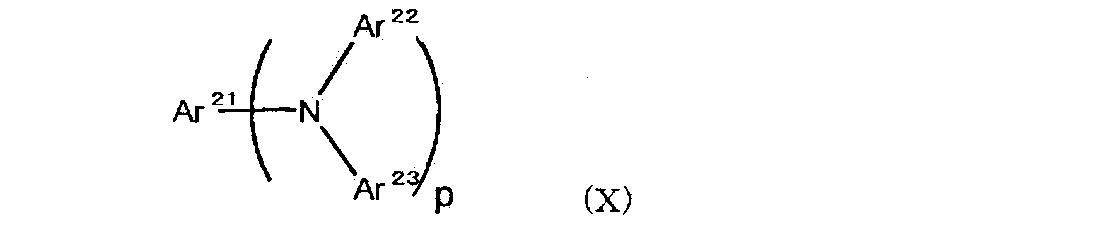
なお、本発明における芳香環基は、芳香族炭化水素環基でもよいし、芳香族複素環基でもよい。


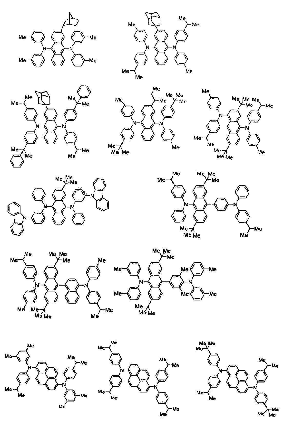

燐光発光材料としては、例えば、長周期型周期表(以下、特に断り書きの無い限り「周期表」という場合には、長周期型周期表を指すものとする。)第7~11族から選ばれる金属を中心金属として含むウェルナー型錯体又は有機金属錯体などが挙げられる。
(式(III)中、Mは金属を表し、qは上記金属の価数を表す。また、L及びL’は二座配位子を表す。jは0、1又は2の数を表す。)


該芳香族炭化水素環基の具体例としては、1個の遊離原子価を有する、ベンゼン環、ナフタレン環、アントラセン環、フェナントレン環、ペリレン環、テトラセン環、ピレン環、ベンズピレン環、クリセン環、トリフェニレン環、アセナフテン環、フルオランテン環、フルオレン環などが挙げられる。
具体例としては、1個の遊離原子価を有する、フラン環、ベンゾフラン環、チオフェン環、ベンゾチオフェン環、ピロール環、ピラゾール環、イミダゾール環、オキサジアゾール環、インドール環、カルバゾール環、ピロロイミダゾール環、ピロロピラゾール環、ピロロピロール環、チエノピロール環、チエノチオフェン環、フロピロール環、フロフラン環、チエノフラン環、ベンゾイソオキサゾール環、ベンゾイソチアゾール環、ベンゾイミダゾール環、ピリジン環、ピラジン環、ピリダジン環、ピリミジン環、トリアジン環、キノリン環、イソキノリン環、シノリン環、キノキサリン環、フェナントリジン環、ベンゾイミダゾール環、ペリミジン環、キナゾリン環、キナゾリノン環、アズレン環などが挙げられる。
具体例としては、1個の遊離原子価を有する、ピロール環、ピラゾール環、イミダゾール環、オキサジアゾール環、インドール環、カルバゾール環、ピロロイミダゾール環、ピロロピラゾール環、ピロロピロール環、チエノピロール環、フロピロール環、チエノフラン環、ベンゾイソオキサゾール環、ベンゾイソチアゾール環、ベンゾイミダゾール環、ピリジン環、ピラジン環、ピリダジン環、ピリミジン環、トリアジン環、キノリン環、イソキノリン環、キノキサリン環、フェナントリジン環、ベンゾイミダゾール環、ペリミジン環、キナゾリン環、キナゾリノン環などが挙げられる。
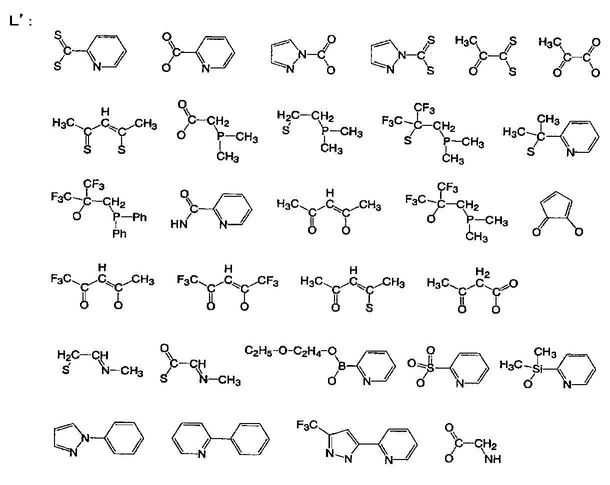
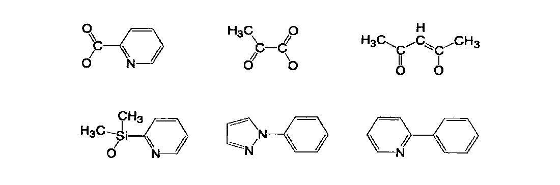


なお、これら置換基は互いに連結して環を形成してもよい。具体例としては、環A1が有する置換基と環A2が有する置換基とが結合するか、又は、環A1’が有する置換基と環A2’が有する置換基とが結合することにより、一つの縮合環を形成してもよい。このような縮合環としては、7,8-ベンゾキノリン基等が挙げられる。


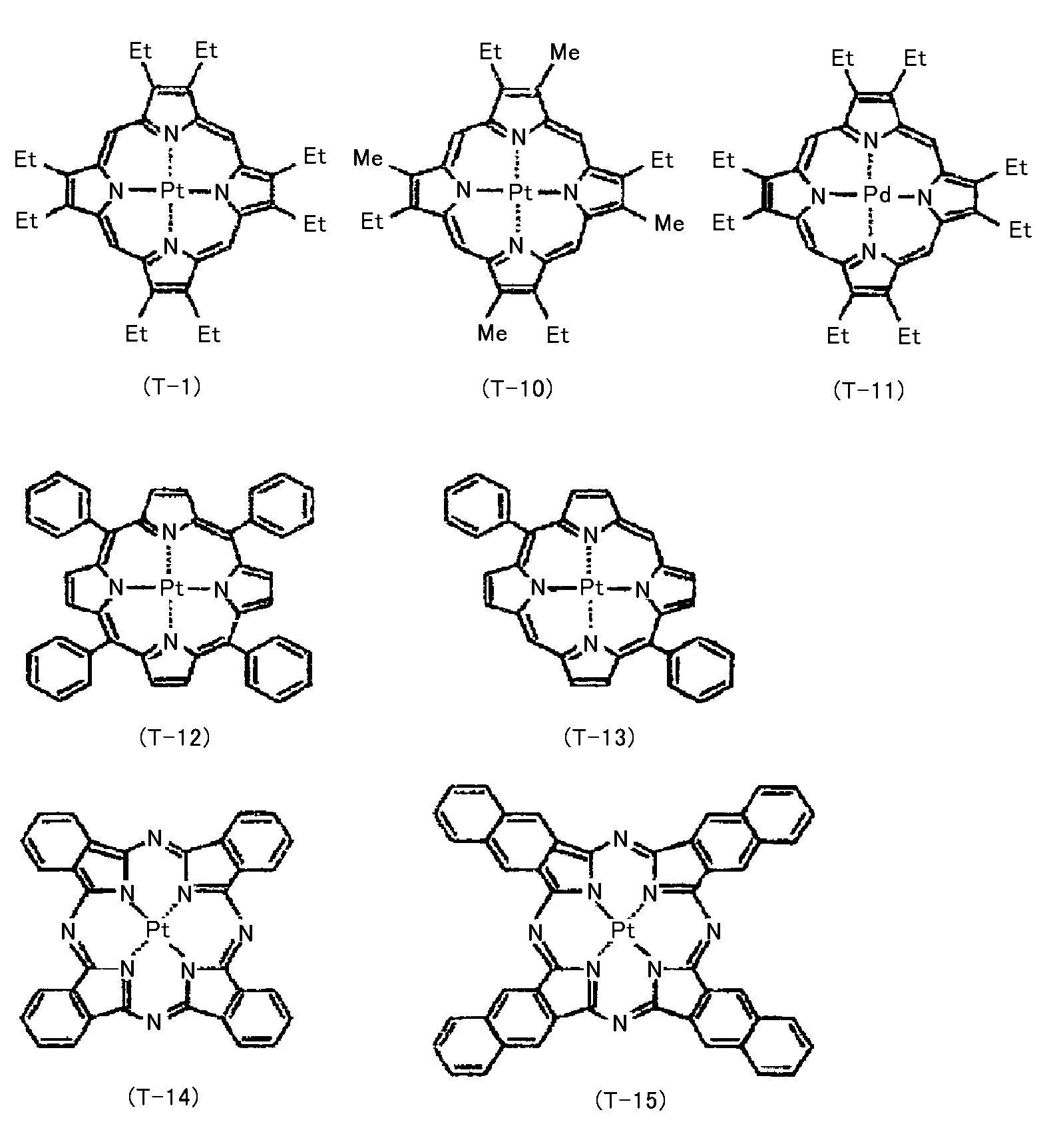
本発明における発光材料の分子量は、本発明の効果を著しく損なわない限り任意である。本発明における発光材料の分子量は、好ましくは10000以下、より好ましくは5000以下、更に好ましくは4000以下、特に好ましくは3000以下である。また、本発明における発光材料の分子量は、通常100以上、好ましくは200以上、より好ましくは300以上、更に好ましくは400以上である。
有機電界発光素子の発光層において、発光材料は、電荷輸送性能を有するホスト材料から電荷又はエネルギーを受け取って発光することが好ましい。従って、発光層は、通常、例えば、このホスト材料として使用されるような、電荷輸送材料を含む。電荷輸送材料には、正孔輸送性を有する化合物(正孔輸送材料或いは正孔輸送性化合物と称することがある)と、電子輸送性を有する化合物(電子輸送材料或いは電子輸送性化合物と称することがある)がある。発光層は、正孔輸送材料と電子輸送材料の両方を含んでいてもよく、いずれか一方を含んでいてもよい。なお、発光層が正孔輸送性を有する化合物は含んでいるが、電子輸送性を有する化合物を含んでいない場合は、発光層において、正孔輸送性を有する化合物が電子を輸送すれば良い。
電子輸送材料は、電子輸送性のユニットを有する化合物であることが好ましい。電子輸送性のユニット(電子輸送ユニット)とは、電子に対する耐久性に優れており、電子輸送性を有する構造(ユニット)である。また、発光層に2種以上の電荷輸送材料が含まれる場合、この電子輸送ユニットを有する化合物が前述の電子輸送を担う電荷輸送材料となりやすい。
電子輸送ユニットとしては具体的には、キノリン環、キナゾリン環、キノキサリン環、フェナントロリン環、ピリジン環、ピリミジン環、ピリダジン環、ピラジン環、トリアジン環、チアジアゾール環、ベンゾチアジアゾール環、キノリノール金属錯体、フェナントロリン金属錯体、ヘキサアザトリフェニレン構造、テトラシアルベンゾキノリン構造等が挙げられる。この中でも電子に対する安定性が高く、電子輸送性が高いことから、好ましくは、キノリン環、キナゾリン環、キノキサリン環、フェナントロリン環、ピリジン環、ピリミジン環、ピリダジン環、ピラジン環、トリアジン環などが挙げられ、中でも電気的安定性に優れる点で好ましくは、キノリン環、キナゾリン環、ピリジン環、ピリミジン環、トリアジン環、1,10-フェナントロリン環などが挙げられる。
この理由は次の通りである。即ち、窒素原子を含む6員環のo-位及びp-位は、活性部位であり、ここが芳香環基によって置換されることで電子が非局在化する。このことで、電子により安定となる。
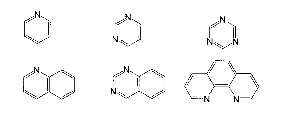
なお、発光層において、電子輸送材料は、1種のみを用いてもよく、2種以上を任意の組み合わせ及び比率で併用してもよい。
正孔輸送材料は、正孔輸送性のユニットを有する化合物であることが好ましい。正孔輸送性のユニット(正孔輸送ユニット)とは、正孔に対する耐久性に優れており、正孔輸送性を有する構造(ユニット)である。
発光層から正孔を取り出し易いイオン化ポテンシャルとは、通常5.4eV以上、好ましくは5.5eV以上、より好ましくは5.6eV以上であり、また、一方、通常6.3eV以下、好ましくは6.2eV、より好ましくは6.1eV以下である。
また、正孔に安定であるとは、正孔輸送ユニットが、ラジカル状態になっても分解され難いということである。これは、ラジカルカチオンが非局在化されることにより、ラジカル状態でも安定化するということである。
正孔輸送ユニットとしては、具体的にはカルバゾール環、フタロシアニン環、ナフタロシアニン構造、ポルフィリン構造、トリアリールアミン構造、トリアリールホスフィン構造、ベンゾフラン環、ジベンゾフラン環、ピレン環、フェニレンジアミン構造、ピロール環、ベンジジン構造、アニリン構造、ジアリールアミン構造、イミダゾリジノン構造、ピラゾール環等が挙げられる。この中でも正孔に対する安定性に優れ、正孔輸送性が高いことから、好ましくは、カルバゾール環、ベンゾフラン環、ジベンゾフラン環、ピレン環、トリアリールアミン構造であり、より好ましくはカルバゾール環、ベンゾフラン環、ジベンゾフラン環、ピレン環であり、特に好ましくはカルバゾール環、ピレン環である。

なお、発光層において、正孔輸送材料は、1種のみを用いてもよく、2種以上を任意の組み合わせ及び比率で併用してもよい。
本発明における電荷輸送材料の分子量は、本発明の効果を著しく損なわない限り任意である。本発明における電荷輸送材料の分子量は、通常10000以下、好ましくは5000以下、より好ましくは4000以下、更に好ましくは3000以下である。また、本発明における電荷輸送材料の分子量は、通常100以上、好ましくは200以上、より好ましくは300以上、更に好ましくは400以上である。
発光層には、上述のような電荷輸送材料の1種のみが含まれていてもよく、2種以上が含まれていてもよい。発光層に2種以上の電荷輸送材料が含まれる場合、主に正孔の輸送を担う電荷輸送材料(正孔輸送材料)のEAに比べて、主に電子輸送を担う電荷輸送材料(電子輸送材料)のEAの方が大きいことが望ましい。即ち、一般的に、同一の層に複数の電荷輸送材料が含まれる場合、電子はEAの大きい材料に乗りやすいため、EAの大きい電荷輸送材料を電子輸送材料とすることで、高発光効率・長寿命の素子を作製する事が可能となる。
電荷輸送材料の化学構造と|EA|との間には、大凡、以下の傾向が認められることが多い。例えば、芳香族性を有する6員環単環を中心に有する材料の場合、ベンゼン環(ヘテロ原子0個)<ピリジン環(ヘテロ原子1個)<ピリミジン環(ヘテロ原子2個)<トリアジン環(ヘテロ原子3個)の順に|EA|が大きくなる傾向がある。また、同じ構造の芳香環の縮環の場合、ベンゼン環(単環)<ナフタレン環(2縮合環)<アントラセン環(3縮合環)<クリセン環(4縮合環)の順に|EA|が大きくなる傾向がある。
本発明に係る発光層は、材料の利用効率が高く、また、その陽極側に形成される正孔輸送層と適度に混ざることにより正孔の注入性が良好となりやすいことから、湿式成膜法で形成されるのが好ましい。
溶剤は、中でも好ましくは、アルカン類や芳香族炭化水素類である。
本発明における発光層形成用組成物は、発光材料を通常0.01重量%以上、好ましくは0.05重量%以上、さらに好ましくは0.1重量%以上含有しているのが良い。また、発光材料を通常20重量%以下、好ましくは10重量%以下、さらに好ましくは5重量%以下含有することが良い。
本発明における発光層形成用組成物は、電荷輸送材料を通常0.1重量%以上、好ましくは0.5重量%以上、さらに好ましくは1重量%以上含有しているのが良い。また、通常20重量%以下、好ましくは10重量%以下、さらに好ましくは5重量%以下含有することが良い。
また、発光層形成用組成物中の発光材料と電荷輸送材料との含有量の比(発光材料/電荷輸送材料の重量比)は、通常0.01以上、好ましくは0.03以上であることが良い。また、発光層形成用組成物中の発光材料と電荷輸送材料との含有量の比(発光材料/電荷輸送材料の重量比)は、通常0.5以下、好ましくは0.2以下であることが良い。
本発明における発光層形成用組成物中の発光材料、正孔輸送材料、電子輸送材料等の合計量である固形分濃度は、膜厚ムラが生じ難い点では少ないことが好ましいが、また、一方で、膜に欠陥が生じ難い点では多いことが好ましい。具体的には、通常0.01重量%以上、通常70重量%以下であることがよい。
発光層の膜厚は本発明の効果を著しく損なわない限り任意であるが、膜に欠陥が生じ難い点では厚いことが好ましいが、また、一方で、駆動電圧が低くなりやすい点では薄いことが好ましい。具体的には、通常3nm以上、好ましくは5nm以上、また、通常200nm以下、好ましくは100nm以下の範囲であるのがよい。
隣接電子輸送層は、発光層と陰極との間に、発光層と隣接して設けられた電子輸送性を有する誘電体の層である。隣接電子輸送層は、陰極から注入された電子を発光層へ輸送する電子輸送性と、発光層へ輸送されてきた正孔が陰極側へ漏れる事を防止する正孔阻止性、又は発光層で発生した励起子が拡散することを防ぐ正孔緩和性を有することが好ましい。隣接電子輸送層の形成方法に制限はない。従って、湿式成膜法、蒸着法や、その他の方法で形成することができる。隣接電子輸送層の膜厚は、本発明の効果を著しく損なわない限り任意であるが、通常0.3nm以上、好ましくは0.5nm以上、また、通常100nm以下、好ましくは50nm以下である。
本発明において、隣接電子輸送層には、電子輸送性、電子の通電に対する耐性及び正孔の通電に対する耐性が必要となるため、隣接電子輸送層を形成する電荷輸送材料としては、好ましくは電子輸送性のユニットと正孔輸送性のユニットとを有する有機化合物が用いられる。ここで、前述の通り、正孔輸送ユニットは、正孔に対する耐久性に優れており、正孔輸送性を有する構造である。また、電子輸送ユニットは、電子に対する耐久性に優れており、電子輸送性を有する構造である。すなわち、本発明に係る隣接電子輸送層には、電気的酸化還元に対する耐久性に優れた電荷輸送材料が含まれていることが好ましい。
正孔輸送ユニット及び電子輸送ユニットが有する構造及び好ましい具体例については、前述の通りである。
正孔輸送ユニットと電子輸送ユニットを介する結合基としては、置換基を有していてもよいアルキレン基、置換基を有していてもよいアルケニレン基及び置換基を有していてもよい2価の芳香族炭化水素環基等が好ましい。

アルキルチオ基の炭素数は、1以上であるのが好ましく、また、一方、20以下であるのが好ましい。具体例としては、メチルチオ基、エチルチオ基、イソプロピルチオ基、シクロヘキシルチオ基等が挙げられる。
隣接電子輸送層に含まれる電荷輸送材料としては、例えば、下記一般式(5)~(7)で表される構造を有する化合物が好ましい。
(B)-(L-A)x (6)
(A)-(L-B)y (7)
(式中、Aは置換基を有していてもよい炭素数1~30の正孔輸送ユニットを示し、Bは置換基を有していてもよい炭素数1~30の電子輸送ユニットを示し、Lは置換基を有していても良い炭素数1~30の炭化水素基を示し、lは0~3の整数を示し、m及びnは各々1~4の整数を示す。l、m及び/又はnが2以上の場合、複数含まれるL、A、Bは、各々同一であっても異なってもよい。また、x及びyは1~4の整数を示し、x又はyが2以上の整数の場合、複数含まれるL-A、L-Bは各々同一であっても異なってもよい。)
なお、一般式(5)及び(6)におけるAは、どちらも1価の基を示し、一般式(7)におけるAは、y価の基を示す。同様に、一般式(5)及び(7)におけるBは、どちらも1価の基を示し、一般式(6)におけるBは、x価の基を示す。一般式(5)における(L)lは、m+n価の基を示し、一般式(6)~(7)におけるLは、何れも2価の基を示す。
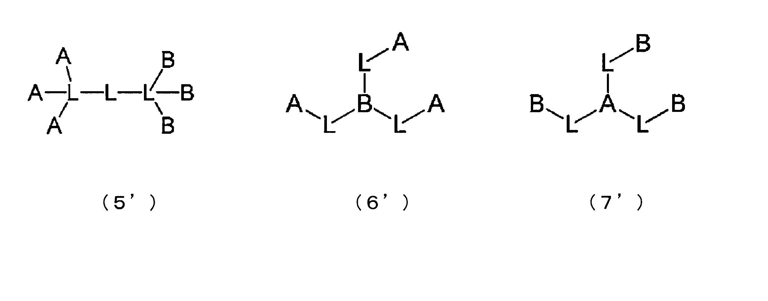
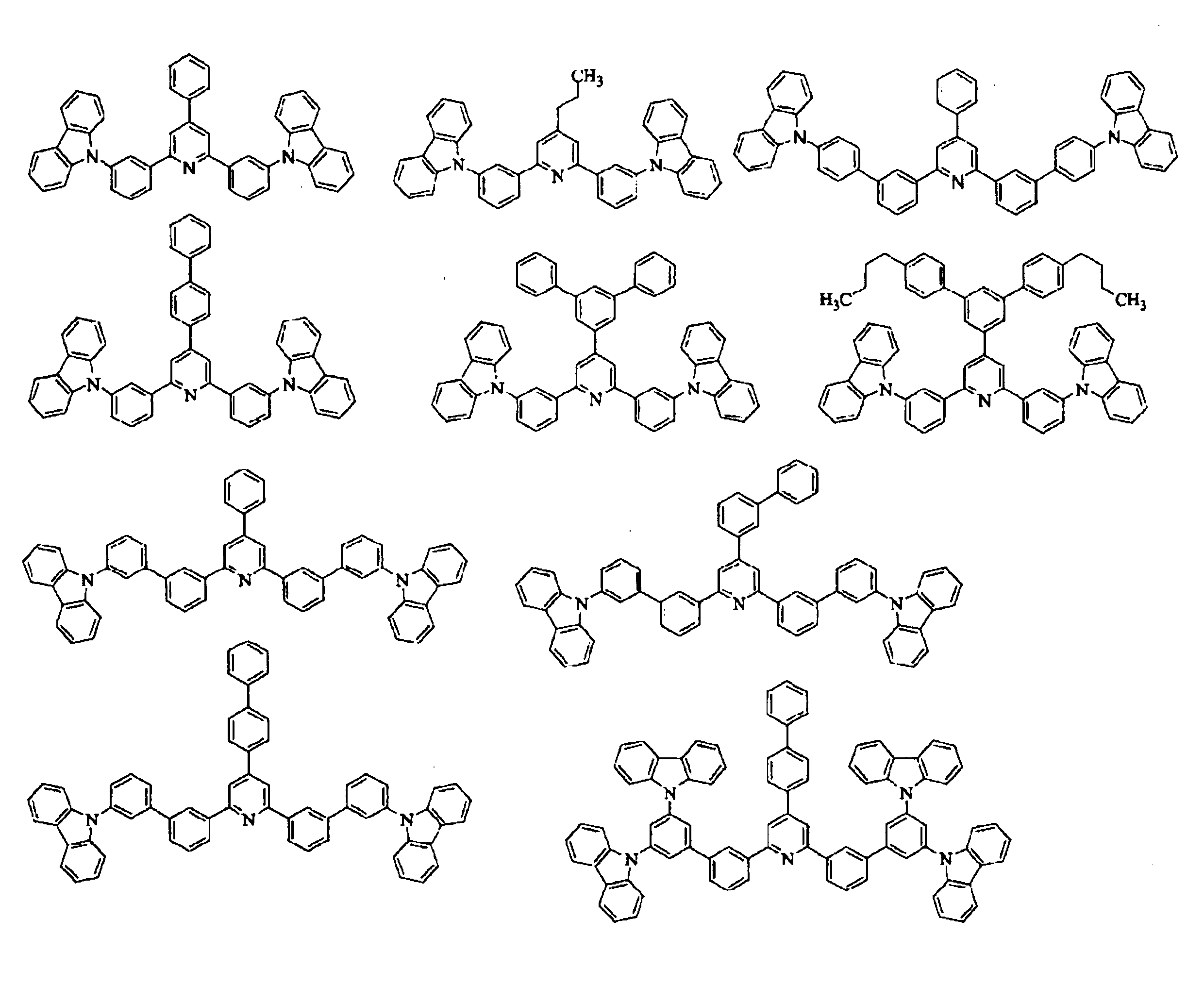
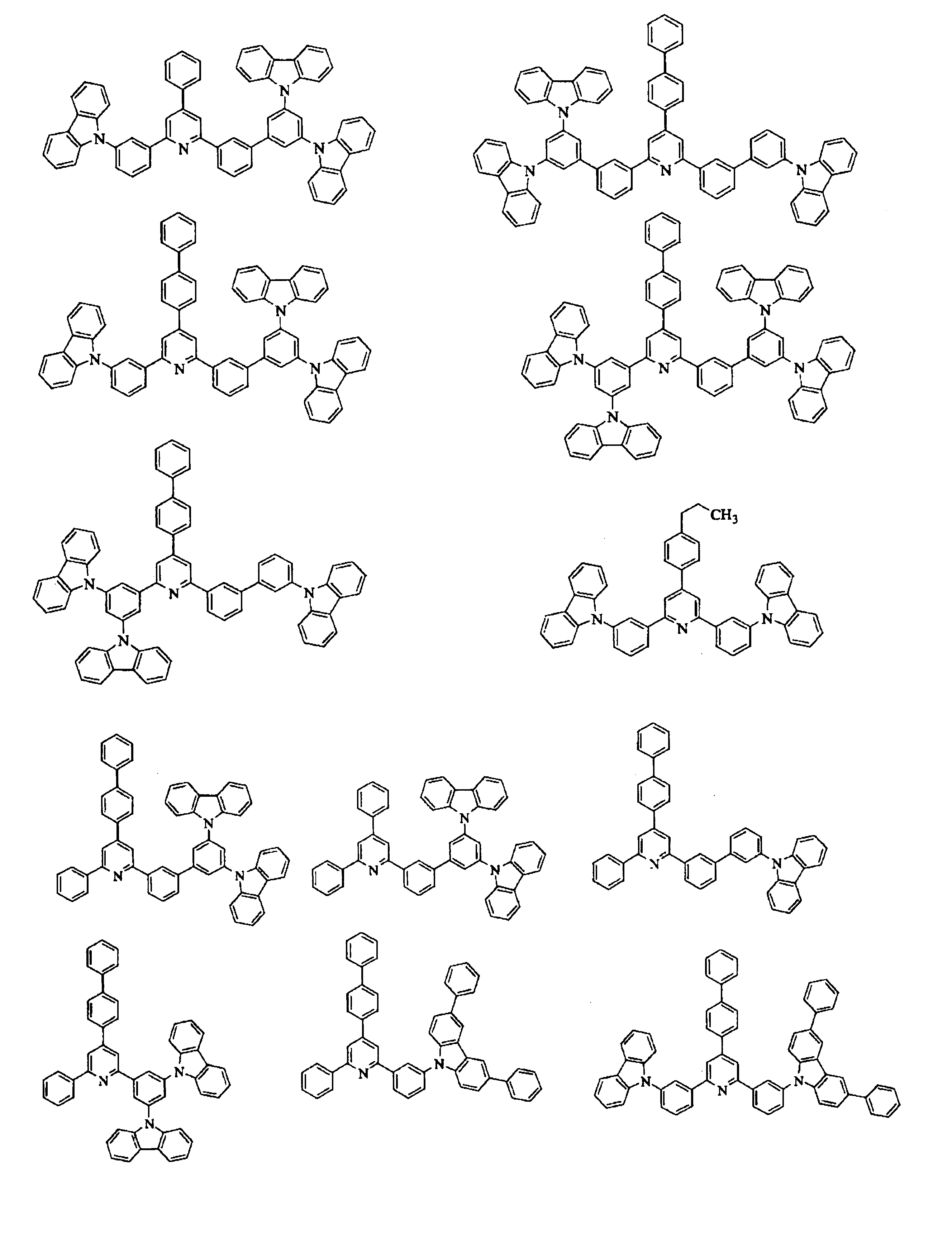
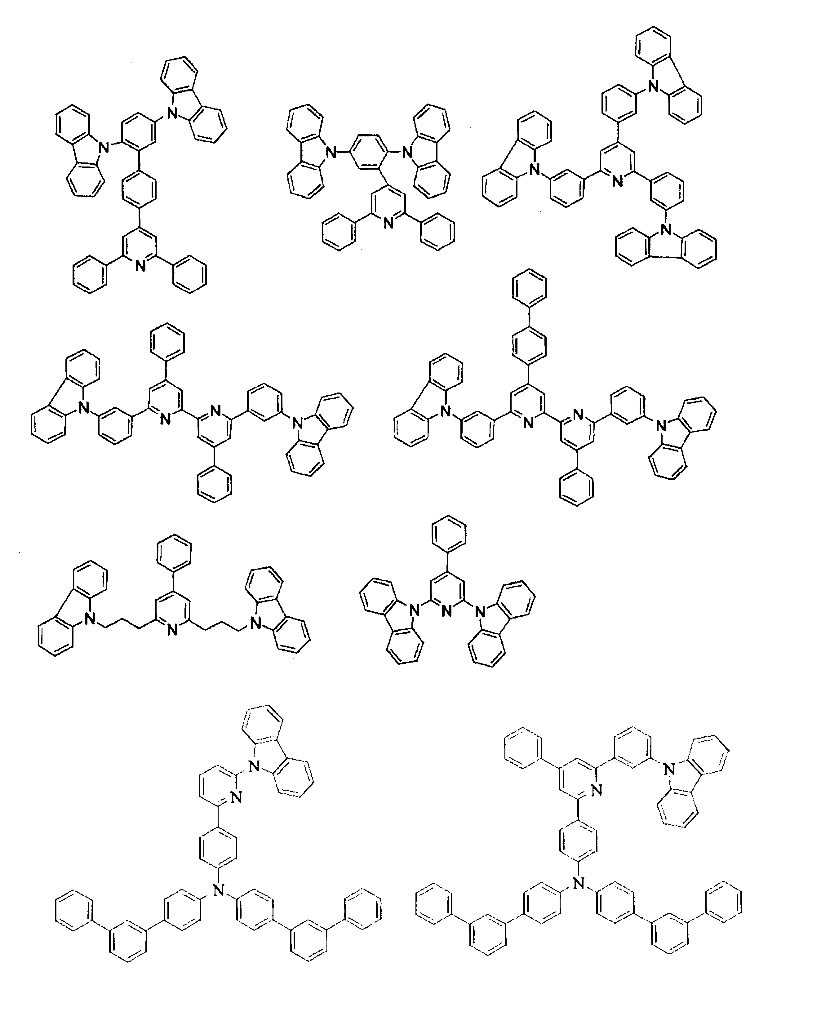

隣接電子輸送層を形成する電荷輸送材料として用いられる有機化合物の分子量は、耐熱性が良好で、ガス発生の原因となりにくく、また精製が容易で、高純度化し易い点で以下の範囲が好ましい。すなわち、通常10000以下、好ましくは5000以下、より好ましくは4000以下、さらに好ましくは3000以下、また、通常100以上、好ましくは200以上、より好ましくは300以上、さらに好ましくは400以上の範囲であるのがよい。
隣接電子輸送層には、上述のような電荷輸送材料の1種のみが含まれていてもよく、2種以上が含まれていてもよい。隣接電子輸送層が2種以上の電荷輸送材料を有する場合、主に正孔の輸送を担う電荷輸送材料(正孔輸送材料)のEAに比べて、主に電子輸送を担う電荷輸送材料(電子輸送材料)のEAの方が大きいことが望ましい。即ち、一般的に、同一の層に複数の電荷輸送材料が含まれる場合、電子はEAの大きい材料に乗りやすいため、EAの大きい電荷輸送材料を電子輸送材料とすることで、高発光効率・長寿命の素子を作製する事が可能となる。
そして、電荷輸送材料の化学構造と|EA|との間には、大凡、上述の傾向が認められることが多い。
本発明の有機電界発光素子は、発光層に含有される電荷輸送材料のうち、電子輸送を担う電荷輸送材料の電子親和力EA1と、隣接電子輸送層に含有される電荷輸送材料のうち、最も絶対値が大きい電子親和力を有する電荷輸送材料の電子親和力EA2とが、下記式(1)、好ましくは下記式(3)で表される関係を満たすことを特徴とする。
式(1):0.00eV≦|EA1|-|EA2|≦0.20eV
式(3):0.00eV<|EA1|-|EA2|≦0.20eV
即ち、本発明の有機電界発光素子は、発光層内の電荷輸送材料の|EA1|が隣接電子輸送層内の電荷輸送材料の|EA2|以上、好ましくは|EA1|が|EA2|より大きいことを特徴とする。
陰極は、発光層側の層に電子を注入する役割を果たす電極である。
陰極の仕事関数(WF)は、大気や水分などに対する安定性である点では大きいことが好ましいが、また、一方、陰極側電子輸送層に対する電子の注入性の点では小さいことが好ましい。具体的には、WFは、2.00eV以上であることが好ましく、2.40eV以上であることが更に好ましく、また、一方、4.90eV以下であることが好ましく、4.80eV以下であることが更に好ましい。
陰極側電子輸送層は、隣接電子輸送層と陰極の間に設けられた電子輸送層であり、隣接電子輸送層と陰極の間に複数の電子輸送層がある場合は、その最も陰極側にある電子輸送層である。
陰極側電子輸送層が2種以上の電荷輸送材料を含有する場合、最も絶対値の大きい電子親和力を有する電荷輸送材料の電子親和力の絶対値を|EA3|とする。
本発明に係る陰極側電子輸送層に含まれる電荷輸送材料のEAの絶対値|EA|は、電子を輸送するエネルギー準位に電子が存在する際に化合物が安定状態となりやすい点では大きいことが好ましいが、また、一方で、安定なラジカルアニオンの形成による電荷の輸送や授受、励起子の生成阻害などが起こり難い点では、小さいことが好ましい。具体的には、隣接電子輸送層中の電荷輸送材料のうち、最もEAの絶対値が大きい電荷輸送材料のEA(隣接電子輸送層中に電荷輸送材料を1種のみ含む場合は当該電荷輸送材料のEA、2種以上の電荷輸送材料を含む場合は、複数の電荷輸送材料のうち、EAの絶対値が最も大きい電荷輸送材料のEA)の絶対値|EA3|は、2.60eV以上であることが好ましく、2.70eV以上であることが更に好ましく、また、一方、3.30eV以下であることが好ましく、3.20eV以下であることが更に好ましい。そして、電荷輸送材料の化学構造と|EA|との間には、大凡、上述の傾向が認められることが多い。
本発明の有機電界発光素子は、陰極の仕事関数の絶対値|WF|と、陰極側電子輸送層内の電荷輸送材料のうち、絶対値が最も大きい電子親和力を有する電荷輸送材料の絶対値|EA(EA3)|との差が所定の範囲内となり、下記式(2)で表される関係を満たすことを特徴とする。
式(2):-1.60eV≦|WF|-|EA3|≦1.60eV
式(4):0.00eV≦|WF|-|EA3|≦1.60eV
以下に、本発明の有機電界発光素子の層構成及びその一般的形成方法等の実施の形態の一例を、図1を参照して説明する。
図1は本発明の有機電界発光素子10の構造例を示す断面の模式図であり、図1において、1は基板、2は陽極、3は正孔注入層、4は正孔輸送層、5は発光層、6は正孔阻止層(隣接電子輸送層)、7は陰極側電子輸送層、8は電子注入層、9は陰極を各々表す。
基板1は、有機電界発光素子の支持体となるものである。基板1としては、石英やガラスの板、金属板や金属箔、プラスチックフィルムやシート等が用いられる。特にガラス板;ポリエステル、ポリメタクリレート、ポリカーボネート、ポリスルホン等の透明な合成樹脂の板が好ましい。合成樹脂基板を使用する場合には、ガスバリア性に留意するのが好ましい。基板のガスバリア性は、基板を通過した外気による有機電界発光素子
の劣化が起こり難いので、大きいことが好ましい。このため、合成樹脂基板の少なくとも片面に緻密なシリコン酸化膜等を設けてガスバリア性を確保する方法も好ましい方法の一つである。
陽極2は、発光層5側の層への正孔注入の役割を果たすものである。
この陽極2は、通常、アルミニウム、金、銀、ニッケル、パラジウム、白金等の金属、
インジウム及び/又はスズの酸化物等の金属酸化物、ヨウ化銅等のハロゲン化金属、カーボンブラック、或いは、ポリ(3-メチルチオフェン)、ポリピロール、ポリアニリン等の導電性高分子等により構成される。
正孔注入層3は、陽極2から発光層5へ正孔を輸送する層である。正孔注入層3は、本発明の有機電界発光素子に必須の層ではないが、正孔注入層3を設ける場合は、正孔注入層3は、通常、陽極2上に形成される。
本発明に係る正孔注入層3の形成方法は、真空蒸着法でも、湿式成膜法でもよく、特に制限はない。正孔注入層3は、ダークスポット低減の観点から湿式成膜法により形成することが好ましい。
正孔注入層3の膜厚は、通常5nm以上、好ましくは10nm以上、また、通常1000nm以下、好ましくは500nm以下の範囲である。
湿式成膜法により正孔注入層3を形成する場合、通常は、正孔注入層3を構成する材料を適切な溶剤(正孔注入層用溶剤)と混合して成膜用の組成物(正孔注入層形成用組成物)を調製し、この正孔注入層3形成用組成物を適切な手法により、正孔注入層の下層に該当する層(通常は、陽極2)上に塗布して成膜し、乾燥することにより正孔注入層3を形成する。
正孔注入層形成用組成物は通常、正孔注入層3の構成材料として正孔輸送材料及び溶剤を含有する。


正孔注入層形成用組成物は、正孔注入層3の構成材料として、電子受容性化合物を含有していることが好ましい。
正孔注入層3の材料としては、本発明の効果を著しく損なわない限り、上述の正孔輸送材料や電子受容性化合物に加えて、さらに、その他の成分を含有させてもよい。その他の成分の例としては、各種の発光材料、電子輸送材料、バインダー樹脂、塗布性改良剤などが挙げられる。なお、その他の成分は、1種のみを用いてもよく、2種以上を任意の組み合わせ及び比率で併用してもよい。
湿式成膜法に用いる正孔注入層形成用組成物の溶剤のうち少なくとも1種は、上述の正孔注入層3の構成材料を溶解しうる化合物であることが好ましい。また、この溶剤の沸点は、通常110℃以上、好ましくは140℃以上、更に好ましくは200℃以上であるのが良く、通常400℃以下、更に好ましくは300℃以下であることが良い。溶剤の沸点は、乾燥速度が速すぎず、膜質に優れる点では、高いことが好ましい。また、一方、溶剤の沸点は、低温乾燥が可能で、他の層や基板に熱の影響を与え難い点では、低いことが好ましい。
正孔注入層3を湿式成膜するときは、通常、正孔注入層形成用組成物を調製後、この組成物を湿式成膜法により、正孔注入層3の下層に該当する層(通常は、陽極2)上に塗布成膜し、乾燥することにより形成する。
塗布するときにおける温度は、組成物中に結晶が生じることによる膜の欠損が起こり難いことから、10℃以上、50℃以下が好ましい。
塗布するときにおける相対湿度は、本発明の効果を著しく損なわない限り限定されないが、通常0.01ppm以上、80%以下である。
真空蒸着により正孔注入層3を形成する場合には、例えば、以下のようにして正孔輸送層3を形成することができる。正孔注入層3の構成材料(前述の正孔輸送材料、電子受容性化合物等)の1種又は2種以上を真空容器内に設置されたるつぼに入れ(2種以上の材料を用いる場合は各々のるつぼに入れ)、真空容器内を適当な真空ポンプで10-4Pa程度まで排気する。この後、るつぼを加熱して(2種以上の材料を用いる場合は各々のるつぼを加熱して)、蒸発量を制御して蒸発させ(2種以上の材料を用いる場合は各々独立に蒸発量を制御して蒸発させ)、るつぼと向き合って置かれた基板1の陽極2上に正孔注入層3を形成させる。なお、2種以上の材料を用いる場合は、それらの混合物をるつぼに入れ、加熱、蒸発させて正孔注入層3を形成することもできる。
正孔輸送層4は、陽極2から発光層5へ輸送する層である。正孔輸送層4は、本発明の有機電界発光素子に必須の層ではないが、正孔輸送層4を設ける場合は、正孔輸送層4は、正孔注入層3がある場合には正孔注入層3の上に、正孔注入層3が無い場合には陽極2の上に形成することができる。
中でも、正孔輸送層4の材料としては、ポリアリールアミン誘導体やポリアリーレン誘導体が好ましい。

中でも、1価の遊離原子価を有する、ベンゼン環由来の基(フェニル基)、ベンゼン環が2環連結してなる基(ビフェニル基)およびフルオレン環由来の基(フルオレニル基)が好ましい。


また、正孔輸送層形成用組成物には、レベリング剤、消泡剤等の塗布性改良剤;電子受容性化合物;バインダー樹脂などを含有していてもよい。
成膜後の加熱の手法は特に限定されない。加熱温度条件としては、通常120℃以上、好ましくは400℃以下である。
発光層5は、電界を与えられた電極間において、陽極2から注入された正孔と、陰極9から注入された電子との再結合により励起されて、主たる発光源となる層である。発光層5は、通常、正孔輸送層4がある場合には正孔輸送層4の上に、正孔輸送層4が無く、正孔注入層3がある場合には正孔注入層3の上に、正孔輸送層4も正孔注入層3も無い場合は、陽極2の上に形成することができる。
発光層の構成材料及び形成方法等については、前述の通りである。
発光層5と後述の電子注入層8との間に、正孔阻止層6を設けてもよい。正孔阻止層6は、電子輸送層のうち、更に陽極2から移動してくる正孔を陰極9に到達するのを阻止する役割をも担う層である。正孔阻止層6は、発光層5の上に、発光層5の陰極9側の界面に接するように積層される層である。本発明の有機電界発光素子においては、正孔阻止層は必須の構成層ではないが、発光層に隣接して正孔阻止層を設けた場合、この正孔阻止層が隣接電子輸送層となる。
なお、正孔阻止層6の材料は、1種のみを用いてもよく、2種以上を任意の組み合わせ及び比率で併用してもよい。
電子輸送層7は、発光層5と後述の陰極9との間に設けられる層である。本発明の有機電界発光素子に、電子輸送層7が2層以上ある場合、このうち、最も陰極側にある層が陰極側電子輸送層となる。また、上述の正孔阻止層6を設けずに電子輸送層を2層以上設ける場合は、このうち、発光層に隣接している層が隣接電子輸送層となる。
電子輸送層7の構成材料及び形成方法等については、前述の陰極側電子輸送層に記載の通りである。
電子輸送層7と後述の陰極9との間に電子注入層8を設けてもよい。電子注入層8は、陰極9から電子輸送層7に電子を注入する(電子の受け渡しを補助する)層である。電子注入層8は、無機塩などの絶縁体(電子輸送性は無い)からなる。
電子注入層8としては、例えばフッ化リチウム(LiF)、フッ化マグネシウム(MgF2)、酸化リチウム(Li2O)、炭酸セシウム(II)(CsCO3)等が挙げられる(Applied Physics Letters, 1997年, Vol.70, pp.152;日本国特開平10-74586号公報;IEEE Transactions on Electron Devices, 1997年,Vol.44, pp.1245;SID 04 Digest, pp.154等参照)。
陰極9は、発光層5側の層(電子注入層8又は発光層5など)に電子を注入する役割を果たす電極である。陰極9は、電源から有機電界発光素子へと電気を供給する回路との導通を取る役割を担う。
陰極9の構成材料及び形成方法等については、前述の陰極の説明に記載の通りである。
本発明に係る有機電界発光素子は、その趣旨を逸脱しない範囲において、別の構成を有していてもよい。具体的には、例えば、その性能を損なわない限り、陽極2と陰極9との間に、上記説明にある層の他に任意の層を有していてもよく、また、上記説明にある層が省略されていてもよい。但し、いずれの場合であっても、発光層と陰極との間に発光層に隣接して設けられる電子輸送層が隣接電子輸送層となり、陰極と発光層との間に陰極に隣接して設けられる電子輸送層が陰極側電子輸送層となる。
電子阻止層を設ける場合は、通常、正孔注入層3又は正孔輸送層4と発光層5との間に設けられる。電子阻止層は、発光層5から移動してくる電子が正孔注入層3に到達するのを阻止することで、発光層5内で正孔と電子との再結合確率を増やし、生成した励起子を発光層5内に閉じこめる役割と、正孔注入層3から注入された正孔を効率よく発光層5の方向に輸送する役割とがある。特に、発光材料として燐光材料を用いたり、青色発光材料を用いたりする場合は、電子阻止層を設けることが効果的である。
本発明の有機電界発光デバイスは、基板上に、互いに異なる色に発光する2種類以上の有機電界発光素子を有する有機電界発光デバイスであって、該有機電界発光素子のうち、少なくとも1種類の有機電界発光素子が、発光層の電荷輸送材料と隣接電子輸送層の電荷輸送材料とが上述の式(1)、好ましくは式(3)を満たし、陰極材料の仕事関数と陰極側電子輸送層の電荷輸送材料とが上述の式(2)を満たす有機電界発光素子であることを特徴とする。
この有機電界発光デバイスにおいて、すべての有機電界発光素子が本発明の有機電界発光素子であることが好ましく、また、有機電界発光素子のうち、少なくとも2種類の有機電界発光素子が有する隣接電子輸送層が同一の材料構成であることが好ましく、同一の材料構成で且つ同一の膜厚であることがさらに好ましい。その理由は、各有機電界発光素子にあわせて隣接電子輸送層を形成する場合に比べて、有機電界発光デバイスを製造する際において、コストダウンが期待できるためである。特に、隣接電子輸送層を蒸着法で形成する場合、各有機電界発光素子にあわせて隣接電子輸送層を形成するためのマスクを設ける必要が無いことは、有機電界発光デバイスを製造する際において、非常に大きなコストダウンにつながる。
本発明の有機EL表示装置は、上述の本発明の有機電界発光素子を用いたものである。本発明の有機EL表示装置の型式や構造については特に制限はなく、本発明の有機電界発光素子を用いて常法に従って組み立てることができる。
例えば、「有機ELディスプレイ」(オーム社、平成16年8月20日発行、時任静士、安達千波矢、村田英幸著)に記載されているような方法で、本発明の有機EL表示装置を形成することができる。
本発明の有機EL照明は、上述の本発明の有機電界発光素子を用いたものである。本発明の有機EL照明の型式や構造については特に制限はなく、本発明の有機電界発光素子を用いて常法に従って組み立てることができる。
・ P1及びH1・・・日本国特開2009-287000号公報に記載の方法に基づいて合成した。
・ eH-3及びeH-7・・・日本国特開2006-188493号公報に記載の方法に基づいて合成した。
・ hH-1・・・日本国特開2011-26237号公報に記載の方法に基づいて合成した。
・ D-1・・・日本国特開2010-202644号公報に記載の方法に基づいて合成した。
・ D-2・・・日本国特願2010-225230号に記載の方法に基づいて合成した。
・ eH-11・・・日本国特開2005-268199号公報に記載の方法に基づいて合成した。
・ eH-4・・・日本国特開2010-235708号公報に記載の方法に基づいて合成した。


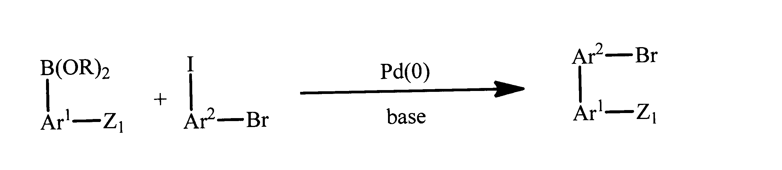
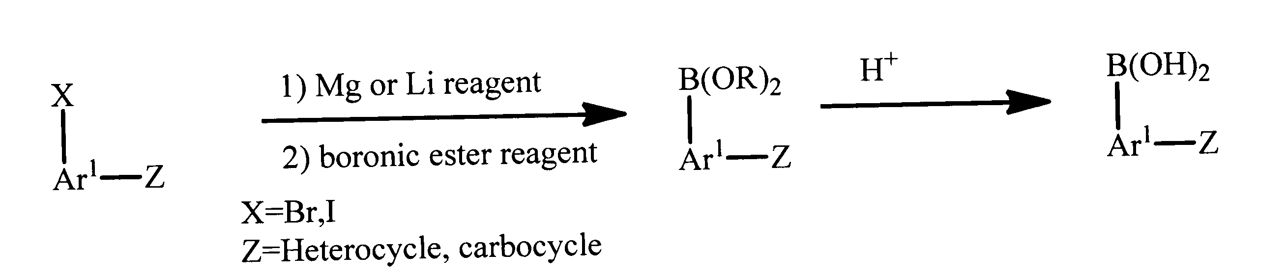
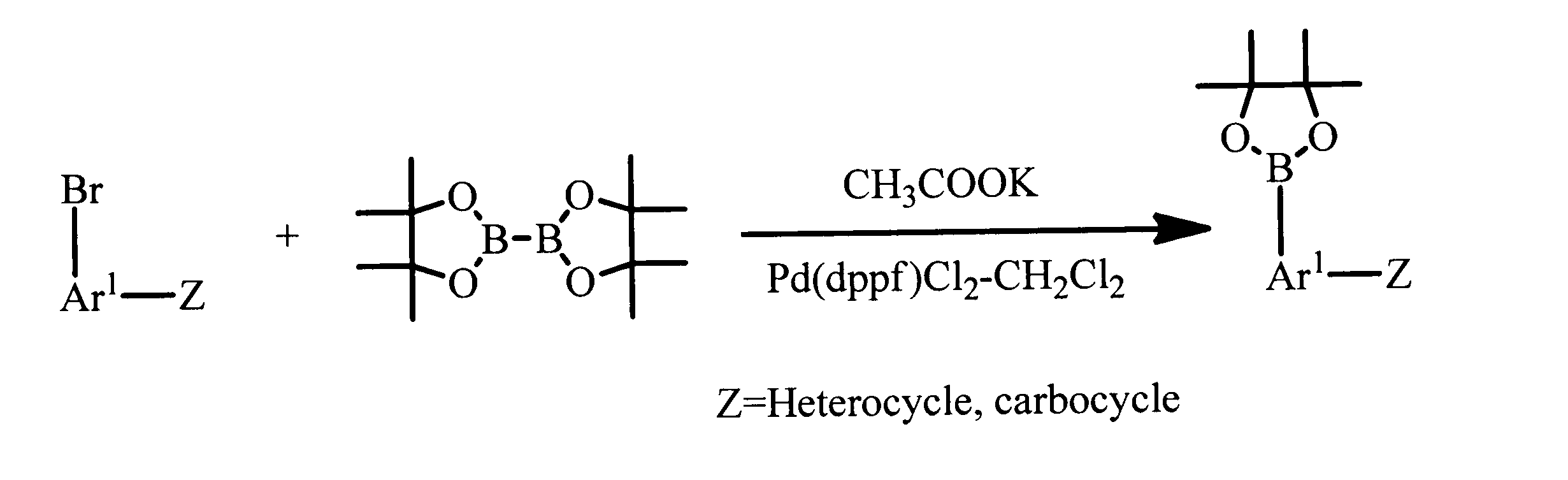

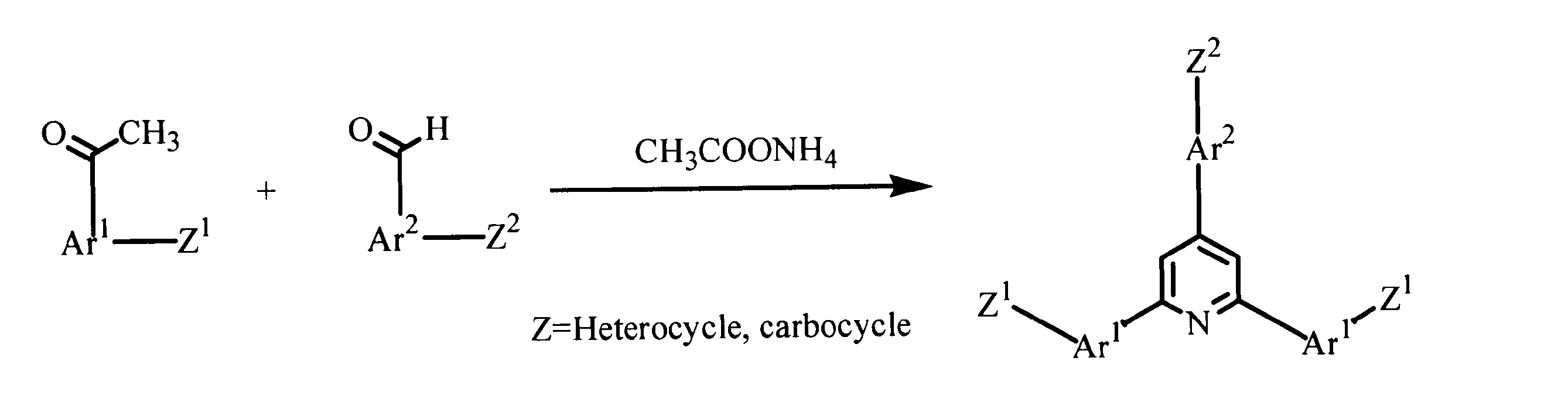


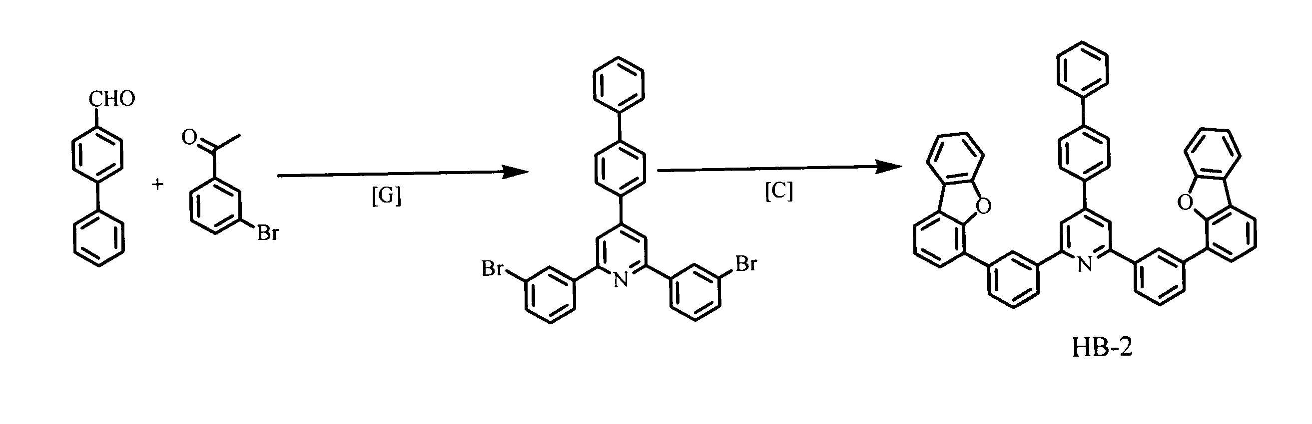

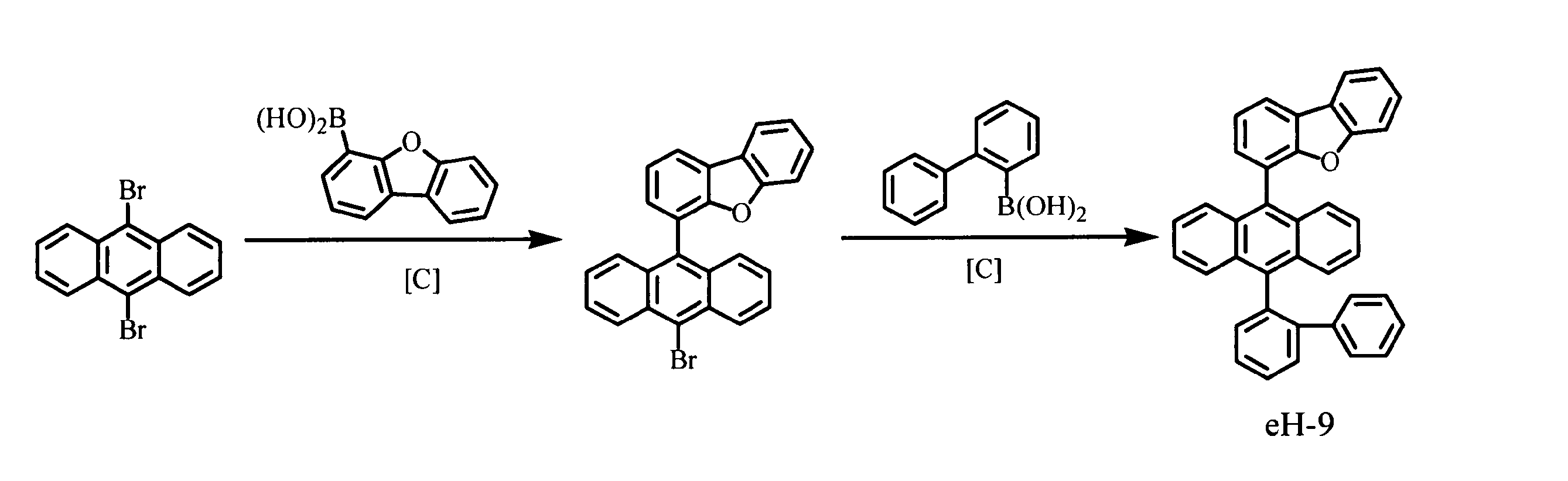
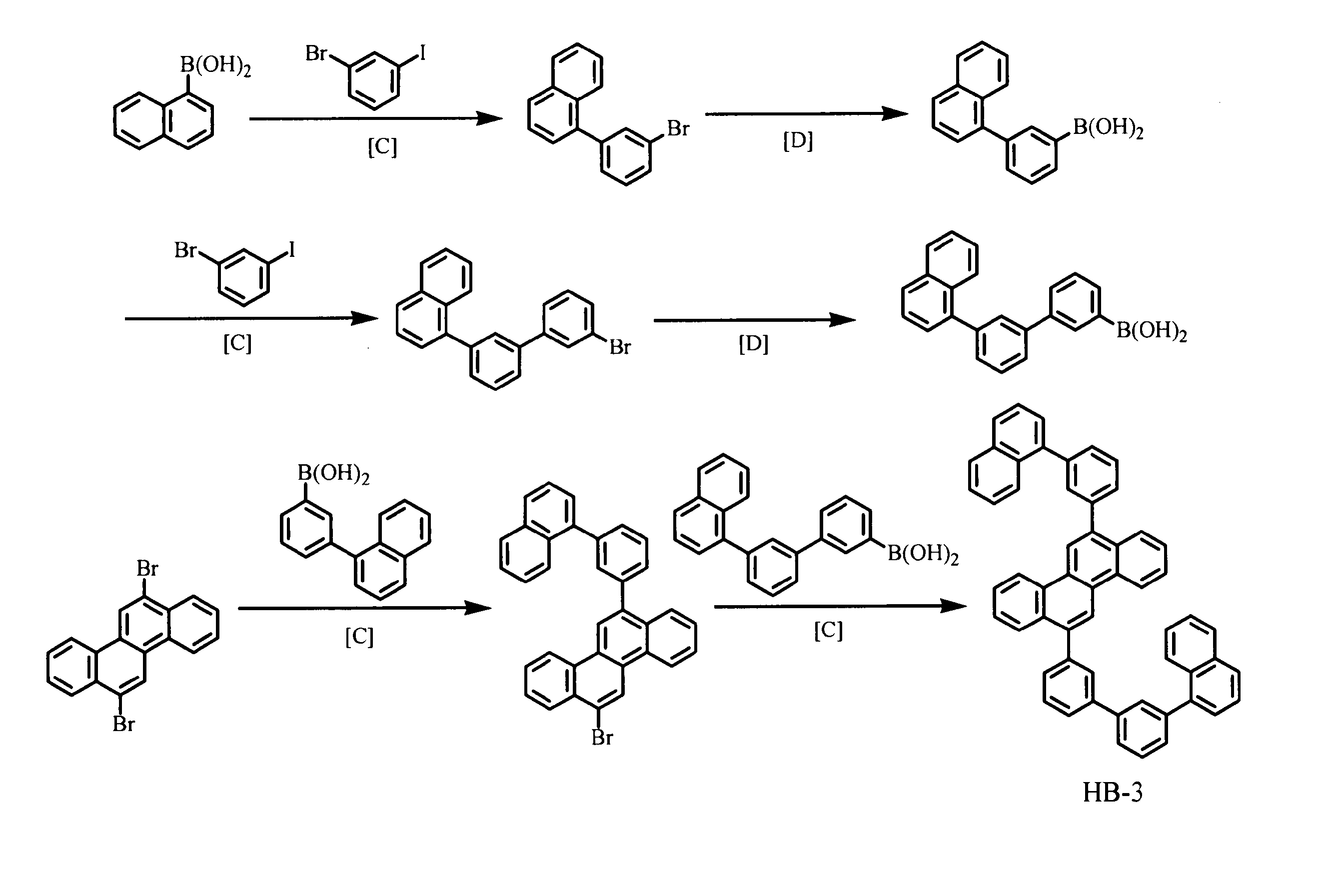

以下の実施例及び比較例において、発光層、隣接電子輸送層である正孔阻止層及び陰極側電子輸送層である電子輸送層に用いた電荷輸送材料について、以下の方法で電子親和力(EA)を測定した。
まず、ガラス基板上に、ITO透明導電膜を70nmの厚さに堆積した基板(三容真空社製、スパッタ成膜品)に対して、界面活性剤水溶液による超音波洗浄、超純水による水洗、超純水による超音波洗浄、超純水による水洗の順で洗浄後、圧縮空気で乾燥させた後、紫外線オゾン洗浄を施した。
各電荷輸送材料(hH-1~hH-3、eH-1、eH-2、eH-4~eH-10、HB-1~HB-4、Alq3)の1重量%トルエン溶液を調製し、この洗浄した基板上にスピンコート法にて下記の条件で成膜することにより、膜厚50nmの電荷輸送材料の膜を得た。また、一部の材料(eH-3及びeH-11)については、前述の洗浄した基板を真空蒸着装置内に搬入し、粗排気を行った後、装置内の真空度が3.0×10⁻⁴Pa以下になるまでクライオポンプを用いて排気し、基板上に電荷輸送材料を真空蒸着法によって積層して電荷輸送材料の薄膜を得た。蒸着時の真空度は、2.2×10⁻⁴Pa以下を保ち、蒸着速度は、0.6~1.2Å/秒の範囲で制御し、膜厚50nmの膜を基板上に形成した。
これらのサンプルについて、オプテル社製「PCR-101」を用いて、10Torr以下まで真空引きした状態で、イオン化ポテンシャルIPを測定した。
同じ工程で成膜したサンプルを用いて、日立社製分光蛍光光度計「F-4500」を用いて、透過光スペクトル、即ち、薄膜吸収スペクトルを測定し、その短波長側の立ち上がり部分で吸収スペクトルとベースラインの接線を引き、該両接線の交点の波長W(nm)から下記式により、バンドギャップEgを算出した。
Eg=1240/W
イオン化ポテンシャルIPとバンドギャップEgの和から、電子親和力の絶対値EAを算出した。結果は、下記表1に示す通りであった。

なお、発光層に1種類しか電荷輸送材料を用いない場合は、表記上電子輸送材料として記載した。
発光層に用いた電荷輸送材料の電荷検出量の比「Q(e)/Q(h)」を以下のようにして測定した。
上述の電子親和力(EA)の測定と同様にして、基板(三容真空社製、スパッタ成膜品)を洗浄した。各電荷輸送材料(hH-1~hH-3及びeH-1~eH-8)の10重量%クロロホルム溶液を作製し、この洗浄した基板上にスピンコート法にて下記の条件で成膜することにより、膜厚2μmの電荷輸送材料の膜を得た。これらのサンプルについて、ITO電極が陽極、対電極が陰極となるように電界強度160kV/cmをかけた状態で、hH-1~hH-3、eH-1、eH-2及びeH-4~eH-8は、日本レーザー社製「Brio(Nd:YAGパルスレーザー)」(励起波長355nm、パルス幅4ns)を、eH-3は、スペクトラフィジクス社製「VSL-337ND-S(窒素レーザー)」(励起波長337nm、パルス幅<4ns)を各々光源に用いて、NDフィルターで20μJに1パルス当たりの光量を調整し、ITO電極側から照射し、その際に流れる電流値をオシロスコープ(テクトロニクス社製「TDS2022」)を用いて測定することにより、正孔の電荷量Q(h)を算出した。また、ITO電極が陰極、対電極が陽極なるようにして、同様の操作を行うことにより、電子の電荷量Q(e)を算出した。この比より、電荷検出量の比「Q(e)/Q(h)」を求めた。結果は、下記表2に示す通りであった。
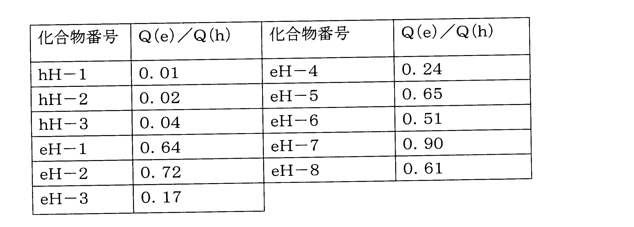
[実施例1]
図1に示す有機電界発光素子を作製した。
まず、ガラス基板上1に、ITO透明導電膜を70nmの厚さに堆積し、2mm幅のストライプにパターニングして、ITOの陽極2を形成した基板(三容真空社製、スパッタ成膜品)について、界面活性剤水溶液による超音波洗浄、超純水による水洗、超純水による超音波洗浄、超純水による水洗の順で洗浄した後、圧縮空気で乾燥させ、紫外線オゾン洗浄を施した。

スピナ回転数 2250rpm
スピナ回転時間 30秒
スピンコート雰囲気 大気雰囲気下
ベーク条件 大気雰囲気下,230℃,1時間

スピナ回転数 1500rpm
スピナ回転時間 120秒
スピンコート雰囲気 窒素雰囲気下
ベーク条件 窒素雰囲気下,230℃,1時間

溶剤 シクロヘキシルベンゼン
成分濃度 (D-1):0.25重量%
(D-2):0.35重量%
(eH-1):1.25重量%
(hH-1):3.75重量%
スピナ回転数 1500rpm
スピナ回転時間 120秒
スピンコート雰囲気 窒素雰囲気下
ベーク条件 窒素雰囲気下,230℃,10分
窒素グローブボックス中で、23mm×23mmサイズのガラス板の外周部に、1mmの幅で光硬化性樹脂30Y-437(スリーボンド社製)を塗布し、中央部に水分ゲッターシート(ダイニック社製)を設置した。この上に、陰極の形成を終了した基板を搬入し、蒸着された面が乾燥剤シートと対向するように貼り合わせた。その後、光硬化性樹脂が塗布された領域のみに紫外光を照射し、樹脂を硬化させた。
発光層において、実施例1で用いた電子輸送材料である(eH-1)の代わりに、以下に示す電子輸送材料(eH-2)を用いた以外は実施例1と同様の方法で有機電界発光素子を作製し、同様に評価を行って、|EA1|-|EA2|の値及び|WF|-|EA3|の値と共に結果を表3及び4にまとめた。

正孔阻止層において、実施例1で用いた電子輸送材料である(eH-1)の代わりに、以下に示す電子輸送材料(eH-5)を用いた以外は実施例1と同様の方法で有機電界発光素子を作製し、同様に評価を行って、|EA1|-|EA2|の値及び|WF|-|EA3|の値と共に結果を表3及び4にまとめた。
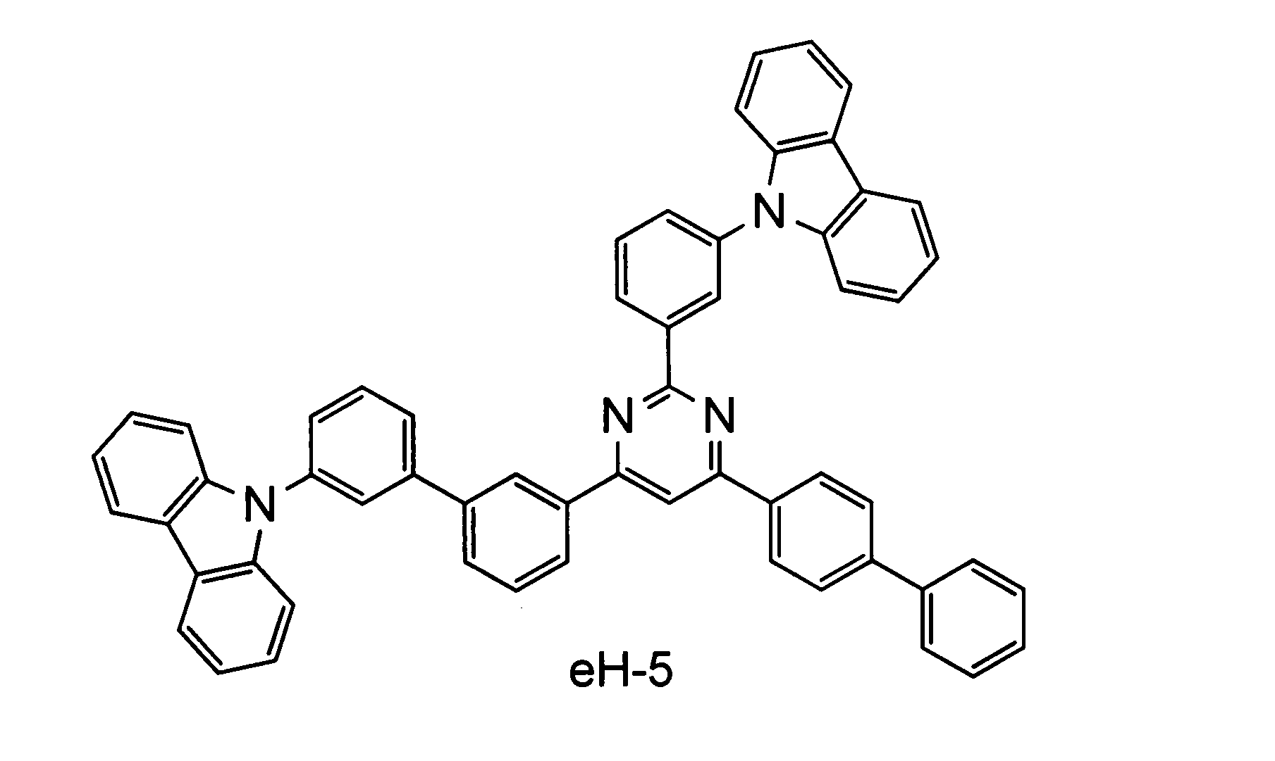
発光層において実施例1で用いた電子輸送材料である(eH-1)の代わりに、以下に示す電子輸送材料(eH-3)を用いた以外は実施例1と同様の方法で有機電界発光素子を作製し、同様に評価を行って、|EA1|-|EA2|の値及び|WF|-|EA3|の値と共に結果を表3及び4にまとめた。

発光層において、実施例1で用いた電子輸送材料である(eH-1)の代わりに前記の電子輸送材料(eH-3)を用いて、正孔輸送材料である(hH-1)の代わりに以下に示す正孔輸送材料(hH-3)を用いて、正孔阻止層で用いた電子輸送材料である(eH-1)の代わりに以下に示す電子輸送材料(HB-1)を用いた以外は、実施例1と同様の方法で有機電界発光素子を作製し、同様に評価を行って、|EA1|-|EA2|の値及び|WF|-|EA3|の値と共に結果を表3及び4にまとめた。

発光層において、実施例1で用いた電子輸送材料である(eH-1)の代わりに以下に示す電子輸送材料(eH-6)を用いて、正孔輸送材料である(hH-1)の代わりに前記の正孔輸送材料(hH-3)を用いて、正孔阻止層で用いた電子輸送材料である(eH-1)の代わりに以下に示す電子輸送材料(HB-2)を用いた以外は、実施例1と同様の方法で有機電界発光素子を作製し、同様に評価を行って、|EA1|-|EA2|の値及び|WF|-|EA3|の値と共に結果を表3及び4にまとめた。

発光層において、実施例1で用いた電子輸送材料である(eH-1)の代わりに以下に示す電子輸送材料(eH-8)を用いて、正孔輸送材料である(hH-1)の代わりに前記の正孔輸送材料(hH-3)を用いて、正孔阻止層で用いた電子輸送材料である(eH-1)の代わりに前記の電子輸送材料(eH-5)を用いた以外は、実施例1と同様の方法で有機電界発光素子を作製し、同様に評価を行って、|EA1|-|EA2|の値及び|WF|-|EA3|の値と共に結果を表3及び4にまとめた。

発光層において、実施例1で用いた電子輸送材料である(eH-1)の代わりに前記の電子輸送材料(eH-6)を用いて、正孔輸送材料である(hH-1)の代わりに前記の正孔輸送材料(hH-3)を用いて、正孔阻止層で用いた電子輸送材料である(eH-1)の代わりに以下に示す電子輸送材料(HB-3)を用いた以外は、実施例1と同様の方法で有機電界発光素子を作製し、同様に評価を行って、|EA1|-|EA2|の値及び|WF|-|EA3|の値と共に結果を表3及び4にまとめた。

発光層において実施例1で用いた電子輸送材料である(eH-1)の代わりに以下に示す電子輸送材料(eH-4)を用いた以外は、実施例1と同様の方法で有機電界発光素子を作製し、同様に評価を行って、|EA1|-|EA2|の値及び|WF|-|EA3|の値と共に結果を表3及び4にまとめた。

発光層において実施例1で用いた発光材料(D-1)、(D-2)の代わりに(D-1)のみを、電子輸送材料(eH-1)の代わりに前記の電子輸送材料(eH-5)を、及び正孔輸送材料(hH-1)の代わりに以下に示す(hH-2)を用い、正孔阻止層において電子輸送材料(eH-1)の代わりに、前記の電子輸送材料(eH-5)を用いた以外は実施例1と同様の方法で有機電界発光素子を作製し、同様に評価を行って、|EA1|-|EA2|の値及び|WF|-|EA3|の値と共に結果を表3及び4にまとめた。
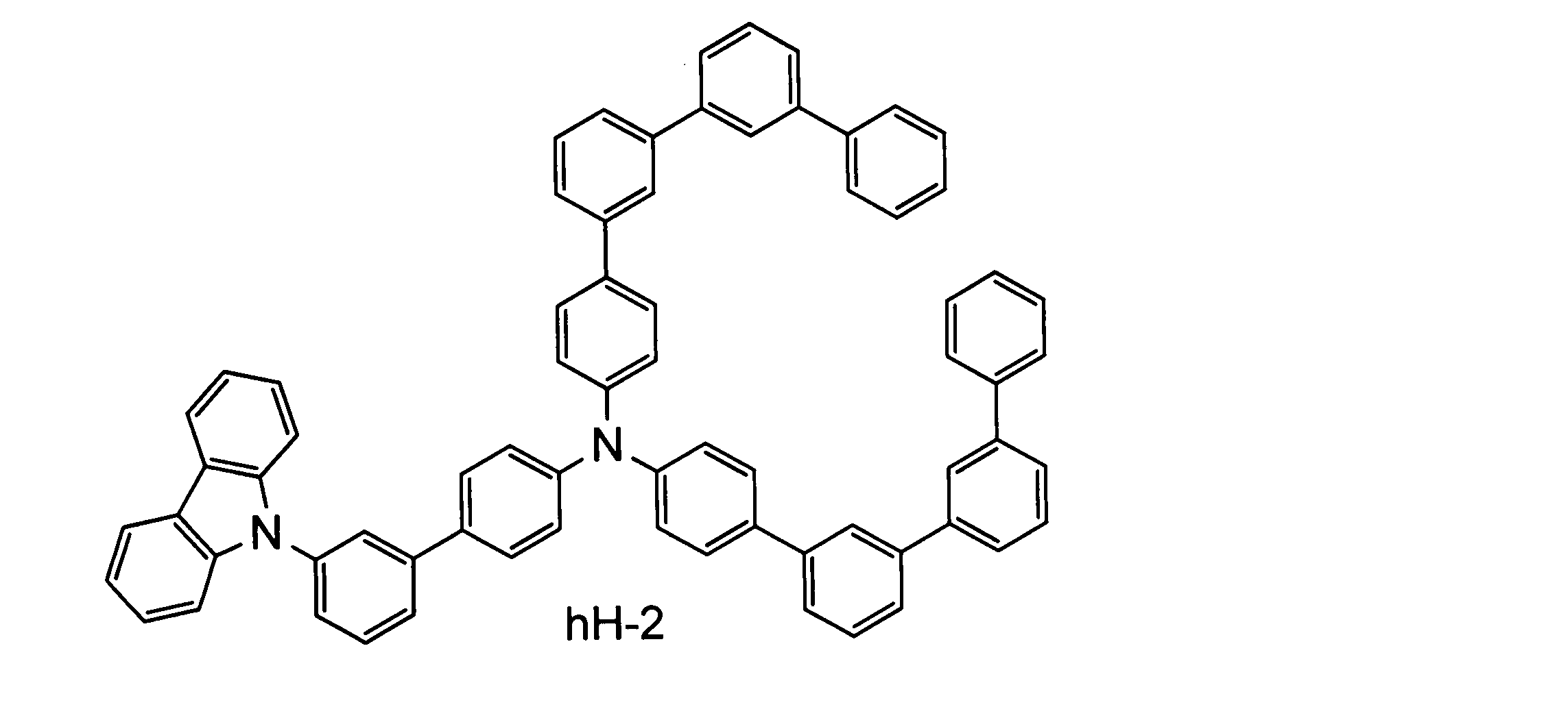
発光層において実施例4で用いた電子輸送材料である(eH-5)の代わりに、前記の電子輸送材料(eH-6)を用いた以外は実施例4と同様の方法で有機電界発光素子を作製し、同様に評価を行って、|EA1|-|EA2|の値及び|WF|-|EA3|の値と共に結果を表3及び4にまとめた。
発光層において実施例4で用いた電子輸送材料である(eH-5)の代わりに、前記の電子輸送材料(eH-2)を用いた以外は実施例4と同様の方法で有機電界発光素子を作製し、同様に評価を行って、|EA1|-|EA2|の値及び|WF|-|EA3|の値と共に結果を表3及び4にまとめた。
発光層において実施例4で用いた電子輸送材料である(eH-5)の代わりに、以下に示す電子輸送材料(eH-7)を用い、正孔輸送材料である(hH-2)の代わりに、正孔輸送材料(hH-3)を用い、正孔阻止層に用いた電子輸送材料(eH-5)の代わりに前記の電子輸送材料(eH-1)を用いた以外は実施例4と同様の方法で有機電界発光素子を作製し、同様に評価を行って、|EA1|-|EA2|の値及び|WF|-|EA3|の値と共に結果を表3及び4にまとめた。

発光層において比較例7で用いた電子輸送材料である(eH-7)の代わりに、前記の電子輸送材料(eH-8)を用いた以外は比較例7と同様の方法で有機電界発光素子を作製し、同様に評価を行って、|EA1|-|EA2|の値及び|WF|-|EA3|の値と共に結果を表3及び4にまとめた。
発光層において比較例7で用いた電子輸送材料である(eH-7)の代わりに、前記の電子輸送材料(eH-6)を用いて、正孔阻止層で用いた電子輸送材料である(eH-1)の代わりに前記の電子輸送材料(HB-3)を用いた以外は比較例7と同様の方法で有機電界発光素子を作製し、同様に評価を行って、|EA1|-|EA2|の値及び|WF|-|EA3|の値と共に結果を表3及び4にまとめた。
発光層において比較例7で用いた電子輸送材料である(eH-7)の代わりに、前記の電子輸送材料(eH-4)を用いた以外は比較例7と同様の方法で有機電界発光素子を作製し、同様に評価を行って、|EA1|-|EA2|の値及び|WF|-|EA3|の値と共に結果を表3及び4にまとめた。
発光層において実施例1で用いた発光材料(D-1)及び(D-2)の代わりに以下に示す(D-3)のみを用い、電子輸送材料(eH-1)の代わりに以下に示す電子輸送材料(eH-9)のみを用い、正孔輸送材料を用いず、正孔阻止層において(eH-1)の代わりに、以下に示す電子輸送材料(eH-9)を用いた以外は実施例1と同様の方法で有機電界発光素子を作製し、同様に評価を行って、|EA1|-|EA2|の値及び|WF|-|EA3|の値と共に結果を表3及び4にまとめた。
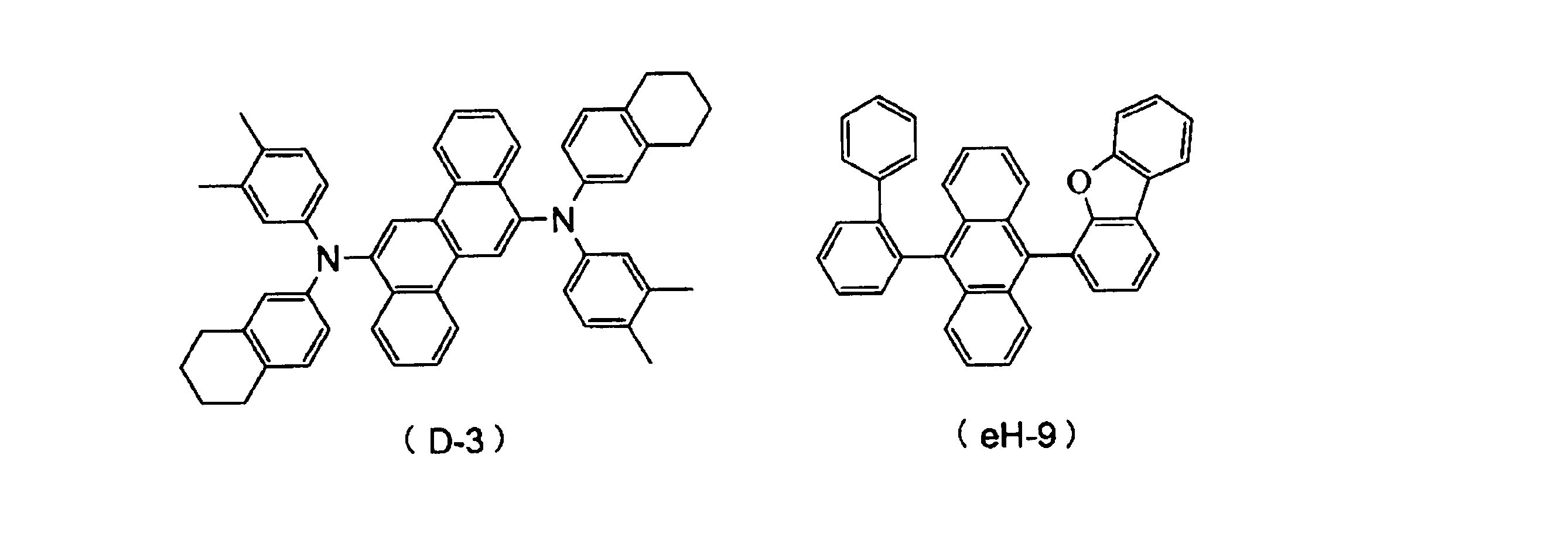
発光層において実施例7で用いた電子輸送材料である(eH-9)の代わりに、以下に示す電子輸送材料(eH-10)を用いた以外は実施例7と同様の方法で有機電界発光素子を作製し、同様に評価を行って、|EA1|-|EA2|の値及び|WF|-|EA3|の値と共に結果を表3及び4にまとめた。

正孔阻止層において実施例7で用いた電荷輸送材料(eH-9)の代わりに、前記の電荷輸送材料(eH-1)を用いた以外は実施例7と同様の方法で有機電界発光素子を作製し、同様に評価を行って、|EA1|-|EA2|の値及び|WF|-|EA3|の値と共に結果を表3及び4にまとめた。
正孔阻止層において実施例7で用いた電荷輸送材料(eH-9)の代わりに、以下に示す電荷輸送材料(eH-11)を用いた以外は実施例7と同様の方法で有機電界発光素子を作製し、同様に評価を行って、|EA1|-|EA2|の値及び|WF|-|EA3|の値と共に結果を表3及び4にまとめた。
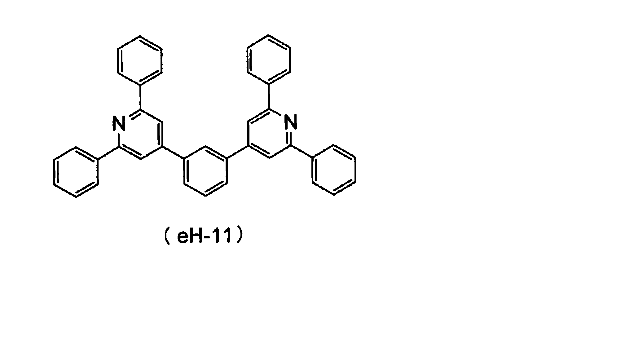
正孔阻止層において実施例7で用いた電荷輸送材料(eH-9)の代わりに、以下に示す電荷輸送材料(HB-4)を用いた以外は実施例7と同様の方法で有機電界発光素子を作製し、同様に評価を行って、|EA1|-|EA2|の値及び|WF|-|EA3|の値と共に結果を表3及び4にまとめた。

正孔阻止層において実施例7で用いた電荷輸送材料(eH-9)の代わりに、前記の電荷輸送材料(eH-6)を用いた以外は実施例7と同様の方法で有機電界発光素子を作製し、同様に評価を行って、|EA1|-|EA2|の値及び|WF|-|EA3|の値と共に結果を表3及び4にまとめた。
発光層において実施例1で用いた電子輸送材料(eH-1)の代わりに前記の電子輸送材料(eH-5)を用いて、正孔輸送材料(hH-1)の代わりに前記の正孔輸送材料(hH-3)を用いて、正孔阻止層において電子輸送材料(eH-1)の代わりに前記の電子輸送材料(eH-3)を用いて、電子輸送層においてAlq3の代わりに前記の電子輸送材料(eH-3)を用いた以外は実施例1と同様の方法で有機電界発光素子を作製し、同様に評価を行って、|EA1|-|EA2|の値及び|WF|-|EA3|の値と共に結果を表3及び4にまとめた。
発光層において実施例4で用いた正孔輸送材料(hH-2)の代わりに前記の正孔輸送材料(hH-3)を用いて、正孔阻止材料(eH-5)の代わりに前記の電子輸送材料(eH-3)を用いて、電子輸送層において電子輸送材料Alq3の代わりに前記の電子輸送材料(eH-3)を用いた以外は、実施例4と同様の方法で有機電界発光素子を作製し、同様に評価を行って、|EA1|-|EA2|の値及び|WF|-|EA3|の値と共に結果を表3及び4にまとめた。
発光層において実施例1で用いた正孔輸送材料(hH-1)の代わりに前記の正孔輸送材料(hH-3)を用いて、電子輸送材料(eH-1)の代わりに前記の電子輸送材料(eH-5)を用いて発光層を形成し、電子輸送材料(eH-1)の代わりに電子輸送材料(eH-3)を用いて正孔阻止層を作製し、電子輸送層において電子輸送材料Alq3の代わりに前記の電子輸送材料(eH-3)とLiFを用いて体積比でeH-3:LiF=94:6となるように共蒸着した層を用いた以外は、実施例1と同様の方法で有機電界発光素子を作製し、同様に評価を行って、|EA1|-|EA2|の値及び|WF|-|EA3|の値と共に結果を表3及び4にまとめた。
発光層において実施例4で用いた正孔輸送材料(hH-2)の代わりに前記の正孔輸送材料(hH-3)を用いて発光層を形成し、電子輸送材料(eH-5)の代わりに前期の電子輸送材料(eH-3)を用いて正孔阻止層を作製し、電子輸送層において電子輸送材料Alq3の代わりに前記の電子輸送材料(eH-3)とLiFを用いて体積比でeH-3:LiF=94:6となるように共蒸着した層を用いた以外は、実施例4と同様の方法で有機電界発光素子を作製し、同様に評価を行って、|EA1|-|EA2|の値及び|WF|-|EA3|の値と共に結果を表3及び4にまとめた。


2 陽極
3 正孔注入層
4 正孔輸送層
5 発光層
6 正孔阻止層
7 電子輸送層
8 電子注入層
9 陰極
10 有機電界発光素子
Claims (10)
- 陽極、発光層、2層以上の電子輸送層及び陰極をこの順に有する有機電界発光素子であって、
該2層以上の電子輸送層の少なくとも1層は該発光層に隣接しており、
該発光層が発光材料及び電荷輸送材料を含有し、
該発光層に隣接している電子輸送層が電荷輸送材料を含有し、
該発光層に含有される電荷輸送材料と該発光層に隣接している電子輸送層に含有される電荷輸送材料は、互いに同一の材料であっても異なる材料であってもよく、
該発光層に含有される電荷輸送材料のうち、電子輸送を担う電荷輸送材料の電子親和力をEA1、
該発光層に隣接している電子輸送層に含有される電荷輸送材料のうち、電子親和力の絶対値が最も大きい電荷輸送材料の電子親和力をEA2としたときに、
EA1とEA2が下記式(1)で表される関係を満たし、
該2層以上の電子輸送層のうち、最も陰極側の電子輸送層に含有される電荷輸送材料のうち、電子親和力の絶対値が最も大きい電荷輸送材料の電子親和力をEA3、
該陰極の仕事関数をWFとしたときに、
EA3とWFが下記式(2)で表される関係を満たす、有機電界発光素子。
式(1): 0.00eV≦|EA1|-|EA2|≦0.20eV
式(2):-1.60eV≦|WF| -|EA3|≦1.60eV - 前記電子親和力EA1と前記電子親和力EA2が下記式(3)で表される関係を満たす、請求項1に記載の有機電界発光素子。
式(3):0.00eV<|EA1|-|EA2|≦0.20eV - 前記電子親和力EA3と前記仕事関数WFが下記式(4)で表される関係を満たす、請求項1又は2に記載の有機電界発光素子。
式(4):0.00eV≦|WF| -|EA3|≦1.60eV - 前記発光層に隣接している電子輸送層が、前記発光層に含有されている電荷輸送材料とは異なる電荷輸送材料を含有している、請求項1乃至3の何れか1項に記載の有機電界発光素子。
- 前記発光層が湿式成膜法により作製された層である、請求項1乃至4の何れか1項に記載の有機電界発光素子。
- 基板上に、互いに異なる色に発光する2種類以上の有機電界発光素子を有する有機電界発光デバイスであって、
該有機電界発光素子のうち、少なくとも1種類の有機電界発光素子が請求項1乃至5の何れか1項に記載の有機電界発光素子である、有機電界発光デバイス。 - 前記有機電界発光素子の全ての有機電界発光素子が請求項1乃至5の何れか1項に記載の有機電界発光素子である、請求項6に記載の有機電界発光デバイス。
- 前記有機電界発光素子のうち、少なくとも2種類の有機電界発光素子が有する前記発光層に隣接している電子輸送層が同一である、請求項6又は7に記載の有機電界発光デバイス。
- 請求項1乃至5の何れか1項に記載の有機電界発光素子を含む、有機EL表示装置。
- 請求項1乃至5の何れか1項に記載の有機電界発光素子を含む、有機EL照明。
Priority Applications (4)
| Application Number | Priority Date | Filing Date | Title |
|---|---|---|---|
| CN201180033220.9A CN102986052B (zh) | 2010-07-08 | 2011-07-07 | 有机电致发光元件、有机电致发光器件、有机el显示装置和有机el照明 |
| KR1020127033845A KR101964998B1 (ko) | 2010-07-08 | 2011-07-07 | 유기 전계 발광 소자, 유기 전계 발광 디바이스, 유기 el 표시 장치 및 유기 el 조명 |
| EP11803663.1A EP2592671B1 (en) | 2010-07-08 | 2011-07-07 | Organic electroluminescent element, organic electroluminescent device, organic el display device, and organic el lighting |
| US13/736,423 US8754399B2 (en) | 2010-07-08 | 2013-01-08 | Organic electroluminescence element, organic electroluminescence device, organic el display device, and organic el lighting |
Applications Claiming Priority (2)
| Application Number | Priority Date | Filing Date | Title |
|---|---|---|---|
| JP2010-155918 | 2010-07-08 | ||
| JP2010155918 | 2010-07-08 |
Related Child Applications (1)
| Application Number | Title | Priority Date | Filing Date |
|---|---|---|---|
| US13/736,423 Continuation US8754399B2 (en) | 2010-07-08 | 2013-01-08 | Organic electroluminescence element, organic electroluminescence device, organic el display device, and organic el lighting |
Publications (1)
| Publication Number | Publication Date |
|---|---|
| WO2012005329A1 true WO2012005329A1 (ja) | 2012-01-12 |
Family
ID=45441306
Family Applications (1)
| Application Number | Title | Priority Date | Filing Date |
|---|---|---|---|
| PCT/JP2011/065598 Ceased WO2012005329A1 (ja) | 2010-07-08 | 2011-07-07 | 有機電界発光素子、有機電界発光デバイス、有機el表示装置及び有機el照明 |
Country Status (7)
| Country | Link |
|---|---|
| US (1) | US8754399B2 (ja) |
| EP (1) | EP2592671B1 (ja) |
| JP (2) | JP2012033918A (ja) |
| KR (1) | KR101964998B1 (ja) |
| CN (1) | CN102986052B (ja) |
| TW (1) | TWI553930B (ja) |
| WO (1) | WO2012005329A1 (ja) |
Cited By (7)
| Publication number | Priority date | Publication date | Assignee | Title |
|---|---|---|---|---|
| WO2014021441A1 (en) * | 2012-08-03 | 2014-02-06 | Semiconductor Energy Laboratory Co., Ltd. | Light-emitting element, light-emitting device, electronic device, and lighting device |
| US20140361252A1 (en) * | 2013-06-10 | 2014-12-11 | Universal Display Corporation | Aluminum chelates as materials for oleds |
| WO2018135656A1 (ja) * | 2017-01-23 | 2018-07-26 | 三菱ケミカル株式会社 | 発光層形成用組成物及び該発光層形成用組成物を含有する有機電界発光素子 |
| JPWO2019088231A1 (ja) * | 2017-11-01 | 2020-11-12 | 出光興産株式会社 | トップエミッション型の有機エレクトロルミネッセンス素子、有機エレクトロルミネッセンス発光装置、及び電子機器 |
| EP3811862A1 (en) | 2019-10-22 | 2021-04-28 | Oxypoint NV | Vital parameter measurements for low care patients |
| WO2021078913A1 (en) | 2019-10-22 | 2021-04-29 | Oxypoint Nv | Vital parameter measurements for low care patients |
| WO2022223676A1 (en) | 2021-04-21 | 2022-10-27 | Oxypoint Nv | System for identifying a condition of a user |
Families Citing this family (13)
| Publication number | Priority date | Publication date | Assignee | Title |
|---|---|---|---|---|
| EP2779263B1 (en) | 2011-11-11 | 2020-12-09 | Mitsubishi Chemical Corporation | Organic electroluminescent element and organic electroluminescent device |
| CN103380508B (zh) | 2011-11-22 | 2017-09-08 | 出光兴产株式会社 | 芳香族杂环衍生物、有机电致发光元件用材料以及有机电致发光元件 |
| JP6217059B2 (ja) * | 2012-07-10 | 2017-10-25 | 三菱ケミカル株式会社 | 有機電界発光素子及び有機電界発光デバイス |
| WO2014054596A1 (ja) | 2012-10-02 | 2014-04-10 | 三菱化学株式会社 | 有機電界発光素子、有機el照明および有機el表示装置 |
| JP2015082537A (ja) * | 2013-10-22 | 2015-04-27 | コニカミノルタ株式会社 | 有機エレクトロルミネッセンス素子、その製造方法及び有機エレクトロルミネッセンスデバイス |
| JP5874860B1 (ja) * | 2015-03-24 | 2016-03-02 | 三菱化学株式会社 | 有機電界発光素子用組成物及び有機電界発光素子の製造方法 |
| EP3306694B1 (en) * | 2015-05-29 | 2020-08-12 | Sumitomo Chemical Company, Ltd. | Light-emitting element and method for manufacturing same |
| WO2017003382A1 (en) * | 2015-07-01 | 2017-01-05 | National University Of Singapore | A n-doped electrically conductive polymeric material |
| KR102577003B1 (ko) * | 2016-06-03 | 2023-09-12 | 삼성디스플레이 주식회사 | 화합물 및 이를 포함하는 유기 발광 소자 |
| JP2019519943A (ja) * | 2016-06-28 | 2019-07-11 | ダウ グローバル テクノロジーズ エルエルシー | 有機電荷輸送膜を作製するためのプロセス |
| US10811636B2 (en) | 2016-11-10 | 2020-10-20 | Int Tech Co., Ltd. | Light emitting device manufacturing method and apparatus thereof |
| TWI669299B (zh) * | 2017-03-08 | 2019-08-21 | Lg Chem, Ltd. | 有機發光裝置 |
| CN111384273B (zh) * | 2018-12-29 | 2021-07-16 | Tcl科技集团股份有限公司 | 一种量子点发光二极管及其制备方法 |
Citations (33)
| Publication number | Priority date | Publication date | Assignee | Title |
|---|---|---|---|---|
| JPS59194393A (ja) | 1983-03-25 | 1984-11-05 | イ−ストマン コダツク カンパニ− | 改良された電力転換効率をもつ有機エレクトロルミネツセント装置 |
| JPH05234681A (ja) | 1990-07-26 | 1993-09-10 | Eastman Kodak Co | 有機エレクトロルミネセンス媒体を有するエレクトロルミネセンス装置 |
| JPH05331459A (ja) | 1992-04-03 | 1993-12-14 | Pioneer Electron Corp | 有機エレクトロルミネッセンス素子 |
| JPH06207169A (ja) | 1992-11-17 | 1994-07-26 | Idemitsu Kosan Co Ltd | 有機エレクトロルミネッセンス素子 |
| JPH0741759A (ja) | 1993-03-26 | 1995-02-10 | Sumitomo Electric Ind Ltd | 有機エレクトロルミネッセンス素子 |
| US5645948A (en) | 1996-08-20 | 1997-07-08 | Eastman Kodak Company | Blue organic electroluminescent devices |
| JPH1074586A (ja) | 1996-07-29 | 1998-03-17 | Eastman Kodak Co | エレクトロルミネセンスデバイスで用いられる二層電子注入電極 |
| JPH1079297A (ja) | 1996-07-09 | 1998-03-24 | Sony Corp | 電界発光素子 |
| JPH10270171A (ja) | 1997-01-27 | 1998-10-09 | Junji Kido | 有機エレクトロルミネッセント素子 |
| JPH11242996A (ja) | 1998-02-25 | 1999-09-07 | Mitsubishi Chemical Corp | 有機電界発光素子 |
| JPH11251067A (ja) | 1998-03-02 | 1999-09-17 | Junji Kido | 有機エレクトロルミネッセント素子 |
| JP2002100478A (ja) | 2000-09-20 | 2002-04-05 | Mitsubishi Chemicals Corp | 有機電界発光素子及びその製造方法 |
| JP2002100482A (ja) | 2000-09-20 | 2002-04-05 | Mitsubishi Chemicals Corp | 有機電界発光素子 |
| JP2003031365A (ja) | 2001-05-02 | 2003-01-31 | Junji Kido | 有機電界発光素子 |
| JP2004006287A (ja) * | 2002-04-12 | 2004-01-08 | Konica Minolta Holdings Inc | 有機エレクトロルミネッセンス素子 |
| WO2004084260A2 (en) | 2003-03-20 | 2004-09-30 | Cambridge Display Technology Limited | Electroluminescent device |
| JP2005022962A (ja) | 2003-06-11 | 2005-01-27 | Mitsubishi Materials Corp | ガラス組成物、混合体、ペースト、グリーンシートおよびpdp |
| WO2005019373A2 (de) | 2003-08-19 | 2005-03-03 | Basf Aktiengesellschaft | Übergangsmetallkomplexe mit carbenliganden als emitter für organische licht-emittierende dioden (oleds) |
| JP2005089024A (ja) | 2003-09-12 | 2005-04-07 | Ricoh Co Ltd | 用紙後処理装置 |
| WO2005089024A1 (ja) | 2004-03-11 | 2005-09-22 | Mitsubishi Chemical Corporation | 電荷輸送膜用組成物及びイオン化合物、それを用いた電荷輸送膜及び有機電界発光素子、並びに、有機電界発光素子の製造方法及び電荷輸送膜の製造方法 |
| JP2005268199A (ja) | 2003-07-31 | 2005-09-29 | Mitsubishi Chemicals Corp | 化合物、電荷輸送材料および有機電界発光素子 |
| JP2006173588A (ja) | 2004-11-17 | 2006-06-29 | Fuji Photo Film Co Ltd | 有機電界発光素子 |
| JP2006188493A (ja) | 2004-12-10 | 2006-07-20 | Pioneer Electronic Corp | 有機化合物、電荷輸送材料および有機電界発光素子 |
| EP1820801A1 (en) | 2004-12-10 | 2007-08-22 | Pioneer Corporation | Organic compound, charge-transporting material, and organic electroluminescent element |
| JP2007302630A (ja) * | 2006-05-12 | 2007-11-22 | Chemiprokasei Kaisha Ltd | ジ−、トリ−またはテトラ−フェニルシラン骨格を有するフルオレン化合物、それを用いた発光層ホスト材料、ホールブロック材料および有機el素子 |
| JP2008098619A (ja) | 2006-09-14 | 2008-04-24 | Sumitomo Chemical Co Ltd | 有機エレクトロルミネッセンス素子 |
| WO2008146800A1 (ja) * | 2007-05-24 | 2008-12-04 | Fujikura Ltd. | 有機el素子及び光インターコネクションモジュール |
| JP2009287000A (ja) | 2008-02-15 | 2009-12-10 | Mitsubishi Chemicals Corp | 共役ポリマー、有機電界発光素子材料、有機電界発光素子用組成物、ポリマーの製造方法、有機電界発光素子、有機elディスプレイ、及び有機el照明 |
| WO2009154168A1 (ja) * | 2008-06-17 | 2009-12-23 | 株式会社日立製作所 | 有機発光素子、その作製方法、その作製装置及びそれを用いた有機発光装置 |
| JP2010202644A (ja) | 2009-02-03 | 2010-09-16 | Mitsubishi Chemicals Corp | 有機金属錯体、有機金属錯体含有組成物、発光材料、有機電界発光素子材料、有機電界発光素子、有機elディスプレイおよび有機el照明 |
| JP2010225230A (ja) | 2009-03-23 | 2010-10-07 | Toshiba Corp | 磁気記録ヘッド、磁気ヘッドアセンブリ及び磁気記録装置 |
| JP2010235708A (ja) | 2009-03-30 | 2010-10-21 | Mitsubishi Chemicals Corp | 蛍光発光材料、有機電界発光素子用組成物、有機電界発光素子、有機elディスプレイ及び有機el照明 |
| JP2011026237A (ja) | 2009-07-24 | 2011-02-10 | Mitsubishi Chemicals Corp | 有機化合物、電荷輸送材料、有機電界発光素子用組成物、有機電界発光素子、有機elディスプレイ及び有機el照明 |
Family Cites Families (32)
| Publication number | Priority date | Publication date | Assignee | Title |
|---|---|---|---|---|
| US6121727A (en) * | 1997-04-04 | 2000-09-19 | Mitsubishi Chemical Corporation | Organic electroluminescent device |
| JP2002289355A (ja) * | 2001-03-26 | 2002-10-04 | Pioneer Electronic Corp | 有機半導体ダイオード及び有機エレクトロルミネセンス素子表示装置 |
| JP2002289353A (ja) * | 2001-03-26 | 2002-10-04 | Pioneer Electronic Corp | 有機半導体ダイオード |
| EP1353388B1 (en) | 2002-04-12 | 2010-03-17 | Konica Corporation | Organic electroluminescence element |
| WO2004082338A1 (ja) * | 2003-03-13 | 2004-09-23 | Fujitsu Limited | 有機エレクトロルミネッセンス素子及び有機エレクトロルミネッセンスディスプレイ |
| JP2005026210A (ja) | 2003-06-10 | 2005-01-27 | Fujitsu Ltd | 有機el素子 |
| JP2005005149A (ja) * | 2003-06-12 | 2005-01-06 | Tohoku Pioneer Corp | 有機el素子及びその製造方法 |
| US6881502B2 (en) | 2003-09-24 | 2005-04-19 | Eastman Kodak Company | Blue organic electroluminescent devices having a non-hole-blocking layer |
| JP2005285619A (ja) * | 2004-03-30 | 2005-10-13 | Seiko Epson Corp | 有機el装置および電子機器 |
| WO2006001469A2 (en) | 2004-06-23 | 2006-01-05 | Sharp Kabushiki Kaisha | Organic electroluminescence device, image display apparatus and lighting apparatus including the same charge transport material |
| JP2006279014A (ja) * | 2004-09-15 | 2006-10-12 | Fuji Photo Film Co Ltd | 有機電界発光素子 |
| JP2006134660A (ja) * | 2004-11-04 | 2006-05-25 | Toshiba Matsushita Display Technology Co Ltd | 有機el素子の製造方法 |
| US20060105202A1 (en) | 2004-11-17 | 2006-05-18 | Fuji Photo Film Co., Ltd. | Organic electroluminescent device |
| JP5092248B2 (ja) * | 2005-02-21 | 2012-12-05 | 三菱化学株式会社 | 有機電界発光素子用組成物、有機電界発光素子用薄膜、有機電界発光素子用薄膜転写用部材、有機電界発光素子及び有機電界発光素子の製造方法 |
| US7683536B2 (en) * | 2005-03-31 | 2010-03-23 | The Trustees Of Princeton University | OLEDs utilizing direct injection to the triplet state |
| US7960038B2 (en) | 2005-05-20 | 2011-06-14 | Semiconductor Energy Laboratory Co., Ltd. | Light emitting device and electronic appliance using the same |
| JP4906073B2 (ja) | 2005-05-20 | 2012-03-28 | 株式会社半導体エネルギー研究所 | 発光装置及びそれを用いた電子機器 |
| JP2007042875A (ja) * | 2005-08-03 | 2007-02-15 | Fujifilm Holdings Corp | 有機電界発光素子 |
| TW200714692A (en) * | 2005-09-30 | 2007-04-16 | Chisso Corp | Emission materials and organic electroluminescent device |
| JP2007266160A (ja) | 2006-03-28 | 2007-10-11 | Canon Inc | 有機発光素子アレイ |
| WO2007123061A1 (ja) * | 2006-04-20 | 2007-11-01 | Idemitsu Kosan Co., Ltd. | 有機発光素子 |
| US7724796B2 (en) * | 2006-08-29 | 2010-05-25 | The Trustees Of Princeton University | Organic laser |
| JP5326093B2 (ja) * | 2006-11-22 | 2013-10-30 | 日本電気株式会社 | 半導体装置及びその製造方法 |
| JP2008214363A (ja) * | 2007-02-28 | 2008-09-18 | Canon Inc | ナノ粒子発光材料、これを用いた電界発光素子及びインク組成物、並びに表示装置 |
| JP2009043684A (ja) * | 2007-08-10 | 2009-02-26 | Toyota Industries Corp | 白色発光有機el(エレクトロルミネッセンス)素子及びその色度調整方法 |
| WO2009123269A1 (ja) * | 2008-04-02 | 2009-10-08 | 三菱化学株式会社 | 高分子化合物、該高分子化合物を架橋させてなる網目状高分子化合物、有機電界発光素子用組成物、有機電界発光素子、有機elディスプレイ及び有機el照明 |
| WO2009123763A2 (en) * | 2008-04-03 | 2009-10-08 | Qd Vision, Inc. | Light-emitting device including quantum dots |
| KR20100021281A (ko) * | 2008-08-14 | 2010-02-24 | 엘지디스플레이 주식회사 | 유기 발광 표시 장치 |
| JP5402472B2 (ja) | 2008-09-30 | 2014-01-29 | 三菱化学株式会社 | 有機薄膜パターニング用基板、有機電界発光素子およびその製造方法、並びに有機el表示装置および有機el照明 |
| CN102197507A (zh) * | 2008-10-28 | 2011-09-21 | 密执安州立大学董事会 | 具有单独的红色、绿色和蓝色子元件的堆叠式白色oled |
| JP2010114232A (ja) * | 2008-11-06 | 2010-05-20 | Nippon Shokubai Co Ltd | 有機電界発光素子 |
| JPWO2010119503A1 (ja) * | 2009-04-14 | 2012-10-22 | シャープ株式会社 | 有機エレクトロルミネッセンス素子およびその製造方法 |
-
2011
- 2011-07-06 JP JP2011150182A patent/JP2012033918A/ja active Pending
- 2011-07-07 WO PCT/JP2011/065598 patent/WO2012005329A1/ja not_active Ceased
- 2011-07-07 KR KR1020127033845A patent/KR101964998B1/ko active Active
- 2011-07-07 EP EP11803663.1A patent/EP2592671B1/en active Active
- 2011-07-07 CN CN201180033220.9A patent/CN102986052B/zh active Active
- 2011-07-08 TW TW100124300A patent/TWI553930B/zh active
-
2013
- 2013-01-08 US US13/736,423 patent/US8754399B2/en active Active
-
2015
- 2015-11-19 JP JP2015226807A patent/JP6191680B2/ja active Active
Patent Citations (33)
| Publication number | Priority date | Publication date | Assignee | Title |
|---|---|---|---|---|
| JPS59194393A (ja) | 1983-03-25 | 1984-11-05 | イ−ストマン コダツク カンパニ− | 改良された電力転換効率をもつ有機エレクトロルミネツセント装置 |
| JPH05234681A (ja) | 1990-07-26 | 1993-09-10 | Eastman Kodak Co | 有機エレクトロルミネセンス媒体を有するエレクトロルミネセンス装置 |
| JPH05331459A (ja) | 1992-04-03 | 1993-12-14 | Pioneer Electron Corp | 有機エレクトロルミネッセンス素子 |
| JPH06207169A (ja) | 1992-11-17 | 1994-07-26 | Idemitsu Kosan Co Ltd | 有機エレクトロルミネッセンス素子 |
| JPH0741759A (ja) | 1993-03-26 | 1995-02-10 | Sumitomo Electric Ind Ltd | 有機エレクトロルミネッセンス素子 |
| JPH1079297A (ja) | 1996-07-09 | 1998-03-24 | Sony Corp | 電界発光素子 |
| JPH1074586A (ja) | 1996-07-29 | 1998-03-17 | Eastman Kodak Co | エレクトロルミネセンスデバイスで用いられる二層電子注入電極 |
| US5645948A (en) | 1996-08-20 | 1997-07-08 | Eastman Kodak Company | Blue organic electroluminescent devices |
| JPH10270171A (ja) | 1997-01-27 | 1998-10-09 | Junji Kido | 有機エレクトロルミネッセント素子 |
| JPH11242996A (ja) | 1998-02-25 | 1999-09-07 | Mitsubishi Chemical Corp | 有機電界発光素子 |
| JPH11251067A (ja) | 1998-03-02 | 1999-09-17 | Junji Kido | 有機エレクトロルミネッセント素子 |
| JP2002100478A (ja) | 2000-09-20 | 2002-04-05 | Mitsubishi Chemicals Corp | 有機電界発光素子及びその製造方法 |
| JP2002100482A (ja) | 2000-09-20 | 2002-04-05 | Mitsubishi Chemicals Corp | 有機電界発光素子 |
| JP2003031365A (ja) | 2001-05-02 | 2003-01-31 | Junji Kido | 有機電界発光素子 |
| JP2004006287A (ja) * | 2002-04-12 | 2004-01-08 | Konica Minolta Holdings Inc | 有機エレクトロルミネッセンス素子 |
| WO2004084260A2 (en) | 2003-03-20 | 2004-09-30 | Cambridge Display Technology Limited | Electroluminescent device |
| JP2005022962A (ja) | 2003-06-11 | 2005-01-27 | Mitsubishi Materials Corp | ガラス組成物、混合体、ペースト、グリーンシートおよびpdp |
| JP2005268199A (ja) | 2003-07-31 | 2005-09-29 | Mitsubishi Chemicals Corp | 化合物、電荷輸送材料および有機電界発光素子 |
| WO2005019373A2 (de) | 2003-08-19 | 2005-03-03 | Basf Aktiengesellschaft | Übergangsmetallkomplexe mit carbenliganden als emitter für organische licht-emittierende dioden (oleds) |
| JP2005089024A (ja) | 2003-09-12 | 2005-04-07 | Ricoh Co Ltd | 用紙後処理装置 |
| WO2005089024A1 (ja) | 2004-03-11 | 2005-09-22 | Mitsubishi Chemical Corporation | 電荷輸送膜用組成物及びイオン化合物、それを用いた電荷輸送膜及び有機電界発光素子、並びに、有機電界発光素子の製造方法及び電荷輸送膜の製造方法 |
| JP2006173588A (ja) | 2004-11-17 | 2006-06-29 | Fuji Photo Film Co Ltd | 有機電界発光素子 |
| JP2006188493A (ja) | 2004-12-10 | 2006-07-20 | Pioneer Electronic Corp | 有機化合物、電荷輸送材料および有機電界発光素子 |
| EP1820801A1 (en) | 2004-12-10 | 2007-08-22 | Pioneer Corporation | Organic compound, charge-transporting material, and organic electroluminescent element |
| JP2007302630A (ja) * | 2006-05-12 | 2007-11-22 | Chemiprokasei Kaisha Ltd | ジ−、トリ−またはテトラ−フェニルシラン骨格を有するフルオレン化合物、それを用いた発光層ホスト材料、ホールブロック材料および有機el素子 |
| JP2008098619A (ja) | 2006-09-14 | 2008-04-24 | Sumitomo Chemical Co Ltd | 有機エレクトロルミネッセンス素子 |
| WO2008146800A1 (ja) * | 2007-05-24 | 2008-12-04 | Fujikura Ltd. | 有機el素子及び光インターコネクションモジュール |
| JP2009287000A (ja) | 2008-02-15 | 2009-12-10 | Mitsubishi Chemicals Corp | 共役ポリマー、有機電界発光素子材料、有機電界発光素子用組成物、ポリマーの製造方法、有機電界発光素子、有機elディスプレイ、及び有機el照明 |
| WO2009154168A1 (ja) * | 2008-06-17 | 2009-12-23 | 株式会社日立製作所 | 有機発光素子、その作製方法、その作製装置及びそれを用いた有機発光装置 |
| JP2010202644A (ja) | 2009-02-03 | 2010-09-16 | Mitsubishi Chemicals Corp | 有機金属錯体、有機金属錯体含有組成物、発光材料、有機電界発光素子材料、有機電界発光素子、有機elディスプレイおよび有機el照明 |
| JP2010225230A (ja) | 2009-03-23 | 2010-10-07 | Toshiba Corp | 磁気記録ヘッド、磁気ヘッドアセンブリ及び磁気記録装置 |
| JP2010235708A (ja) | 2009-03-30 | 2010-10-21 | Mitsubishi Chemicals Corp | 蛍光発光材料、有機電界発光素子用組成物、有機電界発光素子、有機elディスプレイ及び有機el照明 |
| JP2011026237A (ja) | 2009-07-24 | 2011-02-10 | Mitsubishi Chemicals Corp | 有機化合物、電荷輸送材料、有機電界発光素子用組成物、有機電界発光素子、有機elディスプレイ及び有機el照明 |
Non-Patent Citations (18)
| Title |
|---|
| "Ar-Ar Coupling", CHEMICAL REVIEWS,, vol. 95, no. 7, pages 2457 - 2483 |
| "Ar-B Coupling", J. ORG. CHEM.,, vol. 60, no. 23, 1995, pages 7508 - 10 |
| "Boronic Acid Synthesis", JOURNAL OF THE AMERICAN CHEMICAL SOCIETY, vol. 112, no. 22, 1990, pages 8024 - 34 |
| "Coupling Reaction with Pyrimidine Framework", J. ORG. CHEM.,, vol. 66, 2001, pages 7125 - 7128 |
| "Coupling Reaction with Triazine Framework", ORG. LETT.,, vol. 10, no. 5, 2008 |
| "NH-Ar Coupling", J. ORG. CHEM.,, vol. 64, no. 15, 1999 |
| "Pyridine Ring Formation Reaction", J. CHEM. SOC., PERKIN TRANS., vol. 1, 2001, pages 3258 - 3264 |
| "Yiiki-kagaku/Sei-kagaku Meimei-ho (Jo", 1992, NANKODO CO., LTD. |
| APPL. PHYS. LETT., vol. 60, 1992, pages 2711 |
| APPLIED PHYSICS LETTERS, vol. 70, 1997, pages 152 |
| CHEMICAL COMMUNICATIONS, 1996, pages 2175 |
| IEEE TRANSACTIONS ON ELECTRON DEVICES, vol. 44, 1997, pages 1245 |
| JOURNAL OFLUMINESCENCE, vol. 72-74, 1997, pages 985 |
| MICHAEISON; HRBERT B., J APPL. PHYS., vol. 48, 1977, pages 4729 |
| See also references of EP2592671A4 |
| SID 04 DIGEST, 2004, pages 154 |
| SYNTHETIC METALS, vol. 9L, 1997, pages 209 |
| TOKITO SHIZUO; ADACHI CHIHAYA; MURATA HIDEYUKI: "Yuki EL Dispurei", 20 August 2004, OHMSHA, LTD. |
Cited By (20)
| Publication number | Priority date | Publication date | Assignee | Title |
|---|---|---|---|---|
| US11043637B2 (en) | 2012-08-03 | 2021-06-22 | Semiconductor Energy Laboratory Co., Ltd. | Light-emitting element, light-emitting device, electronic device, and lighting device |
| US12295256B2 (en) | 2012-08-03 | 2025-05-06 | Semiconductor Energy Laboratory Co., Ltd. | Light-emitting element, light-emitting device, electronic device, and lighting device |
| US9412962B2 (en) | 2012-08-03 | 2016-08-09 | Semiconductor Energy Laboratory Co., Ltd. | Light-emitting element, light-emitting device, electronic device, and lighting device |
| CN107068913A (zh) * | 2012-08-03 | 2017-08-18 | 株式会社半导体能源研究所 | 发光元件、发光装置、电子设备以及照明装置 |
| WO2014021441A1 (en) * | 2012-08-03 | 2014-02-06 | Semiconductor Energy Laboratory Co., Ltd. | Light-emitting element, light-emitting device, electronic device, and lighting device |
| US10069076B2 (en) | 2012-08-03 | 2018-09-04 | Semiconductor Energy Laboratory Co., Ltd. | Light-emitting element, light-emitting device, electronic device, and lighting device |
| US11968889B2 (en) | 2012-08-03 | 2024-04-23 | Semiconductor Energy Laboratory Co., Ltd. | Light-emitting element, light-emitting device, electronic device, and lighting device |
| US10897012B2 (en) | 2012-08-03 | 2021-01-19 | Semiconductor Energy Laboratory Co., Ltd. | Light-emitting element, light-emitting device, electronic device, and lighting device |
| US9735373B2 (en) * | 2013-06-10 | 2017-08-15 | Universal Display Corporation | Organic electroluminescent materials and devices |
| US20140361252A1 (en) * | 2013-06-10 | 2014-12-11 | Universal Display Corporation | Aluminum chelates as materials for oleds |
| WO2018135656A1 (ja) * | 2017-01-23 | 2018-07-26 | 三菱ケミカル株式会社 | 発光層形成用組成物及び該発光層形成用組成物を含有する有機電界発光素子 |
| KR102544020B1 (ko) | 2017-01-23 | 2023-06-16 | 미쯔비시 케미컬 주식회사 | 발광층 형성용 조성물 및 해당 발광층 형성용 조성물을 함유하는 유기 전계 발광 소자 |
| TWI775802B (zh) * | 2017-01-23 | 2022-09-01 | 日商三菱化學股份有限公司 | 發光層形成用組成物以及含有該發光層形成用組成物的有機電場發光元件 |
| KR20190111919A (ko) * | 2017-01-23 | 2019-10-02 | 미쯔비시 케미컬 주식회사 | 발광층 형성용 조성물 및 해당 발광층 형성용 조성물을 함유하는 유기 전계 발광 소자 |
| JPWO2019088231A1 (ja) * | 2017-11-01 | 2020-11-12 | 出光興産株式会社 | トップエミッション型の有機エレクトロルミネッセンス素子、有機エレクトロルミネッセンス発光装置、及び電子機器 |
| US11456432B2 (en) | 2017-11-01 | 2022-09-27 | Idemitsu Kosan Co., Ltd. | Top emission organic electroluminescent element, organic electroluminescent light emitting device, and electronic device |
| JP7171598B2 (ja) | 2017-11-01 | 2022-11-15 | 出光興産株式会社 | トップエミッション型の有機エレクトロルミネッセンス素子、有機エレクトロルミネッセンス発光装置、及び電子機器 |
| EP3811862A1 (en) | 2019-10-22 | 2021-04-28 | Oxypoint NV | Vital parameter measurements for low care patients |
| WO2021078913A1 (en) | 2019-10-22 | 2021-04-29 | Oxypoint Nv | Vital parameter measurements for low care patients |
| WO2022223676A1 (en) | 2021-04-21 | 2022-10-27 | Oxypoint Nv | System for identifying a condition of a user |
Also Published As
| Publication number | Publication date |
|---|---|
| US20130134402A1 (en) | 2013-05-30 |
| JP2016026416A (ja) | 2016-02-12 |
| JP2012033918A (ja) | 2012-02-16 |
| KR101964998B1 (ko) | 2019-04-02 |
| CN102986052B (zh) | 2016-05-25 |
| CN102986052A (zh) | 2013-03-20 |
| EP2592671B1 (en) | 2019-05-08 |
| EP2592671A1 (en) | 2013-05-15 |
| KR20130095652A (ko) | 2013-08-28 |
| JP6191680B2 (ja) | 2017-09-06 |
| TWI553930B (zh) | 2016-10-11 |
| US8754399B2 (en) | 2014-06-17 |
| EP2592671A4 (en) | 2014-09-03 |
| TW201212330A (en) | 2012-03-16 |
Similar Documents
| Publication | Publication Date | Title |
|---|---|---|
| JP6191680B2 (ja) | 有機電界発光素子、有機電界発光デバイス、有機el表示装置及び有機el照明 | |
| JP6331393B2 (ja) | 有機電界発光素子及び有機電界発光デバイス | |
| JP5549228B2 (ja) | 有機el素子及び有機発光デバイス | |
| JP5743388B2 (ja) | 有機電界発光素子用組成物、有機薄膜、有機電界発光素子、有機el表示装置および有機el照明 | |
| JP5884213B2 (ja) | 有機電界発光素子の製造方法、有機電界発光素子、有機elディスプレイ及び有機el照明 | |
| JP5206900B1 (ja) | 有機電界発光素子、有機電界発光素子用組成物、及び有機電界発光装置 | |
| JP5668330B2 (ja) | 有機電界発光素子、有機el照明及び有機el表示装置 | |
| JP5321700B2 (ja) | 有機電界発光素子、有機el照明および有機el表示装置 | |
| WO2011083588A1 (ja) | 有機el素子及び有機発光デバイス | |
| JP2010183010A (ja) | 有機電界発光素子用組成物、有機薄膜、有機電界発光素子、有機el表示装置および有機el照明 | |
| JP5402703B2 (ja) | 有機電界発光素子、有機elディスプレイ、有機el照明及び有機el信号装置 | |
| JP2014220248A (ja) | 有機電界発光素子の製造方法 | |
| JP5569630B2 (ja) | 有機電界発光素子、有機el照明および有機el表示装置 | |
| JP2010209143A (ja) | 有機電界発光素子用組成物、有機電界発光素子、有機elディスプレイおよび有機el照明 | |
| JP2010209211A (ja) | 有機電界発光素子材料、有機電界発光素子用組成物、有機電界発光素子、有機elディスプレイおよび有機el照明 | |
| JP5708721B2 (ja) | 有機電界発光素子、有機el表示装置および有機el照明 |
Legal Events
| Date | Code | Title | Description |
|---|---|---|---|
| WWE | Wipo information: entry into national phase |
Ref document number: 201180033220.9 Country of ref document: CN |
|
| 121 | Ep: the epo has been informed by wipo that ep was designated in this application |
Ref document number: 11803663 Country of ref document: EP Kind code of ref document: A1 |
|
| ENP | Entry into the national phase |
Ref document number: 20127033845 Country of ref document: KR Kind code of ref document: A |
|
| WWE | Wipo information: entry into national phase |
Ref document number: 2011803663 Country of ref document: EP |
|
| NENP | Non-entry into the national phase |
Ref country code: DE |