WO2012008541A1 - Sonde de contact et unité de détection - Google Patents
Sonde de contact et unité de détection Download PDFInfo
- Publication number
- WO2012008541A1 WO2012008541A1 PCT/JP2011/066141 JP2011066141W WO2012008541A1 WO 2012008541 A1 WO2012008541 A1 WO 2012008541A1 JP 2011066141 W JP2011066141 W JP 2011066141W WO 2012008541 A1 WO2012008541 A1 WO 2012008541A1
- Authority
- WO
- WIPO (PCT)
- Prior art keywords
- contact
- probe
- elastic
- contact probe
- contact portion
- Prior art date
- Legal status (The legal status is an assumption and is not a legal conclusion. Google has not performed a legal analysis and makes no representation as to the accuracy of the status listed.)
- Ceased
Links
Images






Classifications
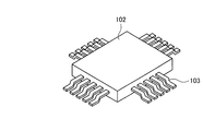
-
- H—ELECTRICITY
- H01—ELECTRIC ELEMENTS
- H01R—ELECTRICALLY-CONDUCTIVE CONNECTIONS; STRUCTURAL ASSOCIATIONS OF A PLURALITY OF MUTUALLY-INSULATED ELECTRICAL CONNECTING ELEMENTS; COUPLING DEVICES; CURRENT COLLECTORS
- H01R13/00—Details of coupling devices of the kinds covered by groups H01R12/70 or H01R24/00 - H01R33/00
- H01R13/02—Contact members
- H01R13/22—Contacts for co-operating by abutting
- H01R13/24—Contacts for co-operating by abutting resilient; resiliently-mounted
- H01R13/2442—Contacts for co-operating by abutting resilient; resiliently-mounted with a single cantilevered beam
-
- G—PHYSICS
- G01—MEASURING; TESTING
- G01R—MEASURING ELECTRIC VARIABLES; MEASURING MAGNETIC VARIABLES
- G01R1/00—Details of instruments or arrangements of the types included in groups G01R5/00 - G01R13/00 and G01R31/00
- G01R1/02—General constructional details
- G01R1/04—Housings; Supporting members; Arrangements of terminals
- G01R1/0408—Test fixtures or contact fields; Connectors or connecting adaptors; Test clips; Test sockets
- G01R1/0433—Sockets for IC's or transistors
- G01R1/0441—Details
- G01R1/0466—Details concerning contact pieces or mechanical details, e.g. hinges or cams; Shielding
-
- H—ELECTRICITY
- H01—ELECTRIC ELEMENTS
- H01R—ELECTRICALLY-CONDUCTIVE CONNECTIONS; STRUCTURAL ASSOCIATIONS OF A PLURALITY OF MUTUALLY-INSULATED ELECTRICAL CONNECTING ELEMENTS; COUPLING DEVICES; CURRENT COLLECTORS
- H01R12/00—Structural associations of a plurality of mutually-insulated electrical connecting elements, specially adapted for printed circuits, e.g. printed circuit boards [PCB], flat or ribbon cables, or like generally planar structures, e.g. terminal strips, terminal blocks; Coupling devices specially adapted for printed circuits, flat or ribbon cables, or like generally planar structures; Terminals specially adapted for contact with, or insertion into, printed circuits, flat or ribbon cables, or like generally planar structures
- H01R12/70—Coupling devices
- H01R12/7076—Coupling devices for connection between PCB and component, e.g. display
-
- H—ELECTRICITY
- H01—ELECTRIC ELEMENTS
- H01R—ELECTRICALLY-CONDUCTIVE CONNECTIONS; STRUCTURAL ASSOCIATIONS OF A PLURALITY OF MUTUALLY-INSULATED ELECTRICAL CONNECTING ELEMENTS; COUPLING DEVICES; CURRENT COLLECTORS
- H01R13/00—Details of coupling devices of the kinds covered by groups H01R12/70 or H01R24/00 - H01R33/00
- H01R13/02—Contact members
- H01R13/22—Contacts for co-operating by abutting
- H01R13/24—Contacts for co-operating by abutting resilient; resiliently-mounted
- H01R13/2435—Contacts for co-operating by abutting resilient; resiliently-mounted with opposite contact points, e.g. C beam
-
- H—ELECTRICITY
- H01—ELECTRIC ELEMENTS
- H01R—ELECTRICALLY-CONDUCTIVE CONNECTIONS; STRUCTURAL ASSOCIATIONS OF A PLURALITY OF MUTUALLY-INSULATED ELECTRICAL CONNECTING ELEMENTS; COUPLING DEVICES; CURRENT COLLECTORS
- H01R13/00—Details of coupling devices of the kinds covered by groups H01R12/70 or H01R24/00 - H01R33/00
- H01R13/40—Securing contact members in or to a base or case; Insulating of contact members
- H01R13/405—Securing in non-demountable manner, e.g. moulding, riveting
-
- H—ELECTRICITY
- H01—ELECTRIC ELEMENTS
- H01R—ELECTRICALLY-CONDUCTIVE CONNECTIONS; STRUCTURAL ASSOCIATIONS OF A PLURALITY OF MUTUALLY-INSULATED ELECTRICAL CONNECTING ELEMENTS; COUPLING DEVICES; CURRENT COLLECTORS
- H01R2201/00—Connectors or connections adapted for particular applications
- H01R2201/20—Connectors or connections adapted for particular applications for testing or measuring purposes
Definitions
- the present invention relates to a contact probe and a probe unit used for connection between electric circuit boards and the like.
- an electrical connection is made between the inspection target and a signal processing device that outputs an inspection signal.
- a probe unit that accommodates a plurality of conductive contact probes is used.
- the probe unit can be applied to highly integrated and miniaturized inspection objects by narrowing the pitch between contact probes with the progress of high integration and miniaturization of semiconductor integrated circuits and liquid crystal panels in recent years. Possible technologies are progressing.
- Wire-type contact probes are easier to reduce in diameter than pin-type contact probes that use springs.
- adjacent contact probes contact each other. Or the contact with the contacted object may vary. For this reason, in the wire-type contact probe, various devices are provided to uniformly align the direction of bending due to the load.
- Patent Document 1 an elastomer made of rubber or resin is provided for the contact probe, and the elastomer is elastically deformed by the contact between the contact probe and the electrode, so that the contact state between the contact probe and the electrode is maintained. is doing.
- Patent Document 2 discloses a probe unit in which a plurality of contact probes having a spring shape and curved in contact with a contact body are accommodated in a test board. In this contact probe, a portion having a spring property and a conducting portion of an electric signal are common.
- the evaluation criteria for the conduction state inspection and the operation characteristic inspection of inspection objects are becoming stricter year by year.
- the use environment temperature at the time of performing these inspections is in a wide range of ⁇ 40 to 200 ° C., and durability at these temperatures is also demanded on the inspection apparatus side including the contact probe.
- the present invention has been made in view of the above, and is a contact probe that has a spring property, can obtain reliable and good conduction between contact objects, and can improve durability in a high temperature region. And it aims at providing a probe unit.
- a contact probe is a plate-like contact probe that connects different substrates, and includes a first contact portion that contacts one substrate, and the other A second contact portion that contacts the substrate, a connection portion that connects the first contact portion and the second contact portion, a conduction portion that conducts electrical conductivity between different substrates, and an operating environment temperature of the contact probe.
- An elastic part that is formed using a metal material having a maximum use temperature equal to or higher than the maximum value, extends from the second contact part, and elastically deforms by a load applied to the first contact part and the second contact part,
- the conducting part includes a conductive material different from the metal material.
- the conductive material is a metal or alloy having a higher electrical conductivity than the metal material.
- the contact probe according to the present invention is characterized in that, in the above-described invention, the conductive portion is formed by laminating the conductive material and the metal material that are plate-shaped with each other in the thickness direction.
- the contact probe according to the present invention is characterized in that, in the above-mentioned invention, the elastic portion is formed by laminating the metal material and the conductive material which are plate-shaped with each other in the thickness direction.
- the first and second contact portions are characterized in that the conductive material protrudes to the outer edge side of the metal material.
- the contact probe according to the present invention is characterized in that, in the above invention, the width of the elastic portion is smaller than the width of the connection portion.
- the contact probe according to the present invention is characterized in that, in the above invention, the metal material is a heat-resistant steel, a superalloy, or an electroformed material.
- the elastic portion includes a first plane in contact with the first contact portion, a parallel to the first plane, and the second contact portion. It is located between the 2nd planes which touch.
- the contact probe according to the present invention is characterized in that, in the above invention, a part of the elastic portion is linear.
- a probe unit according to the present invention includes the contact probe according to the above-described invention and a holding portion that holds the contact probe.
- the contact probe and the probe unit according to the present invention each have a portion having conductivity and a portion having spring property at different positions of the contact probe, and the portion having conductivity is a heat-resistant steel, a superalloy, an electroformed material, or the like. Since the conductive material is different from the portion having the spring property formed by using the metal material, it has the spring property, and reliable and good conduction can be obtained between the contact objects, and the high temperature region. The effect that the durability with respect to can be improved is produced.
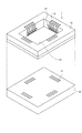
- FIG. 1 is a perspective view showing the configuration of the probe unit according to the first embodiment of the present invention.
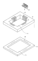
- FIG. 2 is an exploded perspective view showing a configuration of a main part of the probe unit shown in FIG.
- FIG. 3 is an exploded perspective view showing a configuration of a main part of the probe unit shown in FIG.
- FIG. 4 is a perspective view showing a configuration of a main part of the probe unit shown in FIG.
- FIG. 5 is a perspective view showing the contact probe according to the first embodiment of the present invention.
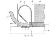
- FIG. 6 is a partial cross-sectional view showing a configuration of a main part of the probe unit shown in FIG.
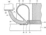
- FIG. 7 is a partial cross-sectional view showing a configuration of a main part of the probe unit shown in FIG. FIG.
- FIG. 8 is a partial cross-sectional view showing a configuration of a main part of the probe unit shown in FIG.
- FIG. 9 is a side view showing a contact probe which is a first modification of the first embodiment of the present invention.
- FIG. 10 is a perspective view showing a contact probe which is a second modification of the first embodiment of the present invention.
- FIG. 11 is a perspective view showing a contact probe which is a third modification of the first embodiment of the present invention.
- FIG. 12 is a perspective view showing a contact probe that is a fourth modification of the first embodiment of the present invention.
- FIG. 13 is a perspective view showing a contact probe which is a fifth modification of the first embodiment of the present invention.
- FIG. 9 is a side view showing a contact probe which is a first modification of the first embodiment of the present invention.
- FIG. 10 is a perspective view showing a contact probe which is a second modification of the first embodiment of the present invention.
- FIG. 11 is a perspective view showing a contact probe
- FIG. 14 is a perspective view showing a contact probe that is a sixth modification of the first embodiment of the present invention.
- FIG. 15 is a perspective view showing a contact probe which is a seventh modification of the first embodiment of the present invention.
- FIG. 16 is a perspective view showing a contact probe according to the second embodiment of the present invention.
- FIG. 17 is a partial cross-sectional view showing the configuration of the main part of the probe unit according to the second embodiment of the present invention.
- FIG. 18 is a partial cross-sectional view showing the configuration of the main part of the probe unit according to the second embodiment of the present invention.
- FIG. 19 is a perspective view showing a semiconductor integrated circuit which is a modification of the embodiment of the present invention.
- FIG. 1 is a perspective view showing the configuration of the probe unit according to the first embodiment of the present invention.
- a probe unit 1 shown in FIG. 1 is a device that is used when an electrical characteristic test is performed on a semiconductor integrated circuit 100 that is an object to be tested, and a circuit that outputs a test signal to the semiconductor integrated circuit 100 and the semiconductor integrated circuit 100.
- This is an apparatus for electrically connecting the substrate 30.
- the semiconductor integrated circuit 100 is described as being a QFN (Quad Flat Non-Leaded Package) having the electrode 101.
- the probe unit 1 includes a conductive contact probe 20 (hereinafter simply referred to as a “probe 20”) that contacts two different objects to be contacted (substrates), that is, a semiconductor integrated circuit 100 and a circuit board 30, and a plurality of probes 20. It has a probe holder 10 as a holding part that receives and holds it in accordance with a predetermined pattern, and a circuit board 30 that abuts on the bottom of the probe holder 10 and outputs a test signal to the semiconductor integrated circuit 100 via the probe 20. .
- a conductive contact probe 20 hereinafter simply referred to as a “probe 20”
- probe 20 that contacts two different objects to be contacted (substrates), that is, a semiconductor integrated circuit 100 and a circuit board 30, and a plurality of probes 20. It has a probe holder 10 as a holding part that receives and holds it in accordance with a predetermined pattern, and a circuit board 30 that abuts on the bottom of the probe holder 10 and output
- the circuit board 30 has an electrode 31 for outputting a test signal to the semiconductor integrated circuit 100 via the probe 20 as shown in FIG.
- the electrode 31 is disposed on the circuit board 30 corresponding to the probe 20 held by the probe holder 10.
- the probe holder 10 and the circuit board 30 may be connected by screws or the like, or may be bonded by an adhesive or a seal member. Any bonding form is possible as long as the contact between the probe 20 and the electrode 31 is not hindered.
- the probe holder 10 is formed using an insulating material, and includes a housing portion 11 in which a housing space capable of housing the semiconductor integrated circuit 100 is formed, and a slit 12 for holding the probe 20 in a predetermined pattern.
- the slit 12 holds the probe 20 so that the tip of the probe 20 protrudes toward the accommodating portion 11 side. Further, when the semiconductor integrated circuit 100 is accommodated in the accommodating portion 11, the slit 12 is formed at a position where each probe 20 contacts the electrode 101 of the corresponding semiconductor integrated circuit 100.
- FIG. 3 is an exploded perspective view showing a configuration of a main part of the probe unit 1 shown in FIG.
- FIG. 4 is a perspective view showing a configuration of a main part of the probe unit 1 shown in FIG.
- the probe holder 10 is configured by detachably connecting a fixing member 13 that fixes the probe 20 to the outer periphery of the bottom.
- the fixing member 13 is formed using an insulating material and has an opening 15 that is larger than the probe holder 10 and a hole 14 that holds and fixes the probe 20.
- the probe holder 10 has a rectangular parallelepiped shape by fitting with the fixing member 13 at a notch corresponding to the fixing member 13 and constitutes a holding portion that holds the probe 20.
- the hole portion 14 accommodates the end portion of the probe 20 inserted through the slit 12, and holds the probe 20 so that the other tip portion of the probe 20 is positioned at a predetermined position of the accommodation portion 11. If the probe 20 can be fixed at a predetermined interval and in a predetermined direction, the holding portion may be configured only by the fixing member 13, and the probe unit 10 and the hole portion 14 of the fixing member 13 are integrally formed. Also good.
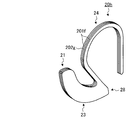
- FIG. 5 is a perspective view showing the probe 20 according to the first embodiment of the present invention.
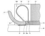
- 6 is a cross-sectional view taken along a plane passing through the center of the slit 12 shown in FIG.
- the probe 20 shown in FIGS. 5 and 6 is formed by laminating a metal plate 201 and a metal plate 202 having a substantially flat plate shape with a uniform plate thickness in the thickness direction, and has a side surface that forms an arc shape at the tip.
- the first contact portion 21 that contacts the semiconductor integrated circuit 100 at the side surface
- the second contact portion 22 that has an arc-shaped side surface and contacts the circuit board 30 at the side surface, the first contact portion 21 and the second contact portion.
- the elastic part which extends from the 2nd contact part 22, the part which comprises arc shape, and is elastically deformed with the load added to the 1st contact part 21 and the 2nd contact part 22 has the strip
- the arc-shaped side surface of the second contact portion 22 is held by the probe holder 10 and comes into contact with the electrode 31 of the circuit board 30 as shown in the cross-sectional view of FIG.
- the elastic part 24 has a smaller width than the width of the connection part 23. For this reason, the elastic portion 24 is more likely to be elastically deformed than the other portions with respect to the load applied to the first contact portion 21 or the second contact portion 22.
- the ratio between the width of the elastic part 24 and the width of the connecting part 23 may be any ratio as long as the elastic part 24 can be preferentially elastically deformed.
- the end portion of the elastic portion 24 in a direction different from the second contact portion 22 extends in a straight line shape, and the tip end portion of the straight line portion is inserted into the hole portion 14 so that the probe 20 is attached to the probe portion. It is held by the holder 10.
- Examples of the metal material forming the metal plate 201 include heat-resistant steel, superalloy, or electroformed material having a maximum use temperature of 200 ° C. or more when the maximum value of the use environment temperature is about 200 ° C.
- Examples of the heat resistant steel include austenitic stainless steel, alloy tool steel, precipitation hardening stainless steel, and the like.
- Examples of the superalloy include a nickel base superalloy, a cobalt base superalloy, and a nickel-cobalt superalloy, which are alloys mainly composed of nickel base and cobalt base.
- a metal having a melting point of 600 ° C. or more can be used.
- An example of such a metal is a nickel-based electroformed material.
- the maximum use temperature is an amount obtained from the linear shrinkage ratio with respect to heating, and is an amount indicating the heat resistance characteristics of the material.
- Examples of the metal forming the metal plate 202 include a conductive material such as a metal or an alloy having an electric resistivity of 1.0 ⁇ 10 ⁇ 7 ⁇ ⁇ m or less.
- Examples of the metal include gold, copper, nickel, silver, platinum, and rhodium. Note that any metal or alloy having higher electrical conductivity than the metal material forming the metal plate 201 is applicable.
- the metal plate 201 suppresses the deformation of the probe 20 due to the elastic deformation of the elastic portion 24 being maintained in a high temperature state, and the metal plate 202 reliably Good electrical conduction can be performed.
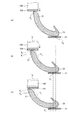
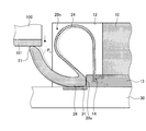
- FIG. 7 is a partial cross-sectional view showing a state in which a load is applied to the first contact portion 21 or the second contact portion 22.
- FIG. 7 when the first contact portion 21 contacts the electrode 101 of the semiconductor integrated circuit 100 and a load is applied in the direction of the arrow in the figure, the curved portion of the elastic portion 24 is elastically deformed.
- broken lines P 0 indicates the position of the probe 20 in a state where no load is applied as shown in FIG.
- the first contact portion 21 and the second contact portion 22 are not elastically deformed and contact the electrodes 101 and 31 according to the load. Move while touching. Further, the elastic portion 24 undergoes elastic deformation in accordance with a load transmitted via the connection portion 23 and the second contact portion 22. In addition, the conduction
- FIG. 8 shows a contact state between the first contact portion 21 and the electrode 101 and a contact state between the second contact portion 22 and the electrode 31 when a load is applied to the first contact portion 21 and the elastic portion 24 is elastically deformed.
- FIG. 8A shows a state where the electrode 101 of the semiconductor integrated circuit 100 is in contact with the first contact portion 21 (a state where no load is applied). In this case, the contact point between the first contact portion 21 and the electrode 101 is S 0 , and the contact point between the second contact portion 22 and the electrode 31 is C 0 .
- FIG. 8A when the semiconductor integrated circuit 100 moves in the direction of the arrow, a load is applied to the first contact portion 21 and the first contact portion 21 is pushed down. Due to the movement of the first contact portion 21, the contact points of the first contact portion 21 and the second contact portion 22 with the electrodes 101 and 31 are shifted to S 1 and C 1 respectively (FIG. 8B).
- the broken line P 0 indicates the position of the probe 20 in a state where no load is applied as shown in FIG. 8A, and the broken line I 0 indicates the position of the semiconductor integrated circuit 100 shown in FIG. Yes.
- each contact part 21 and the second contact portion 22 rotate on the electrodes 101 and 31, and the contact points move. For this reason, each contact part has a small frictional force applied to each electrode, and can suppress wear of the contact part and each electrode.
- the probe unit 1 In the probe unit 1 according to the first embodiment described above, different metals are laminated, and the portion that conducts electricity in the same probe and the portion having spring properties are made different from each other.
- the probe can be designed without a long conduction path, ensuring reliable electrical continuity, and preventing deformation of the probe due to repeated use at high temperatures or prolonged pressurization. It becomes.
- each contact part rotates with respect to a contact with an electrode and moves a contact, the friction between a contact part and an electrode can be reduced and abrasion of a contact part and an electrode can be suppressed.
- the stacked relationship between the metal plate 201 and the metal plate 202 may be reversed, or a configuration in which one metal plate 201 and the metal plate 202 are bonded together may be used. And the structure by which the some metal plate of four or more layers is laminated
- stacked may be sufficient.
- the probe according to the first embodiment described above has a configuration in which the elastic plate 24 side is formed of the metal plate 201 and the conductive portion is formed of the metal plate 202, and then the metal plate 201 and the metal plate 202 are connected. May be.
- FIG. 9 is a plan view showing a probe 20a which is a first modification of the first embodiment.
- the metal plate 202 that conducts electrical continuity between the first contact portion 21a and the second contact portion 22a is obtained from the metal plate 201.
- FIG. 10 is a perspective view showing a probe 20b that is a second modification of the first embodiment.
- a metal plate 202a formed of the above-described material for forming the metal plate 202 is laminated on a portion corresponding to the conductive portion with respect to the metal plate 201 having the above-described shape.
- FIG. 11 is a perspective view showing a probe 20c, which is a third modification of the first embodiment.
- the elastic portion 25 is formed to be curved so that the straight portions on both ends are parallel. Further, the radius of curvature of the curved portion of the elastic portion 25 is smaller than the radius of curvature of the elastic portion 24 shown in FIG. Note that the width of the elastic portion 25 is smaller than the width of the connecting portion 23.
- the probe 20c described above is effective when the device is downsized because the curved portion of the elastic portion 25 is small. Further, when the contact direction of the probe 20 and the semiconductor integrated circuit 100 is the direction as shown in FIGS. 7 and 8, the formation region of the curved portion of the elastic portion 25 with respect to the moving direction of the semiconductor integrated circuit 100 is the connection portion. Since it does not overlap with the formation region of 23, the probe can be further miniaturized by shortening the connecting portion 23.
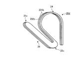
- FIG. 12 is a perspective view showing a probe 20d that is a fourth modification of the first embodiment.
- the probe 20d is formed by laminating a metal plate 201b and a metal plate 202c corresponding to the metal plate 201 and the metal plate 202, respectively, and the first contact portion 21 and the second contact described above.
- an elastic portion 24 that is elastically deformed by a load applied to the first contact portion 21c and the second contact portion 22c.
- the probe 20d has the same effect as that of the first embodiment described above, and the radius of curvature of the contact portion with the electrode of the second contact portion 22c is small, and the distance to rotate on the electrode is shortened. Useful when the size is small. Further, since the connection portion 26 has a shorter conduction distance than the arc-shaped connection portion 23 described above, it is possible to obtain more stable conduction.
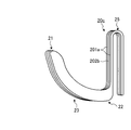
- FIG. 13 is a perspective view showing a probe 20e that is a fifth modification of the first embodiment.
- the probe 20e is formed by laminating a metal plate 201c and a metal plate 202d corresponding to the metal plate 201 and the metal plate 202, respectively, and the first contact portion 21 and the second contact described above.
- an elastic portion 27 that is elastically deformed by a load applied to. Note that the width of the elastic portion 27 is smaller than the width of the connecting portion 23. Moreover, the edge part of the direction different from the 2nd contact part 22 of the elastic part 27 is extended linearly.
- the elastic portion 27 is positioned between the first plane G 1 that is in contact with the first contact portion 21 and the second plane G 2 that is parallel to the first plane G 1 and is in contact with the second contact portion 22. To do. That is, the elastic portion 27, the second plane G 2, the distance d2 to the farthest point in the second plane G 2 of the elastic portion 27, the first plane G 1 and the second plane G 2 It is curved and formed to be smaller than the distance d1 between them.
- the probe 20e has the same effect as that of the first embodiment described above. For example, when the probe 20e is held by the probe holder 1 to perform an inspection, the semiconductor integrated circuit 100 from above in a region including the region where the elastic portion 27 is formed. Even when the two approaches, the elastic part 27 and the semiconductor integrated circuit 100 can be inspected without contact.
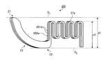
- a probe 20f having an elastic portion 27a having a shape that extends in a zigzag shape by repeating curved portions having opposite concavities and convexities may be used.
- the probe 20f is formed by laminating a metal plate 201d and a metal plate 202e corresponding to the metal plate 201 and the metal plate 202, respectively.
- Elastic portion 27a is reciprocally in a direction substantially orthogonal to the plane G 1, G 2, a shape extending in a direction parallel to the plane G 1, G 2.
- the second plane G 2 the distance d3 to the second point farthest to the plane G 2 of the resilient portion 27a, the distance between the first plane G 1 and the second plane G 2 It is curved and formed so as to be smaller than d1.
- a probe 20g having an elastic portion 27b having a shape that extends in a zigzag shape by repeating curved portions having opposite concavities and convexities may be used.
- the probe 20g is formed by laminating a metal plate 201e and a metal plate 202f corresponding to the metal plate 201 and the metal plate 202, respectively.
- Elastic portion 27b is to reciprocate in a direction parallel to the plane G 1, G 2, a shape extending in the plane G 1, G 2 and perpendicular.
- the second plane G 2 the distance d4 to the second point farthest to the plane G 2 of the elastic portion 27b, the distance between the first plane G 1 and the second plane G 2 It is curved and formed so as to be smaller than d1.
- the shapes of the elastic portions 27, 27a, 27b according to the above-described modified examples 5 to 7 can also be applied to the elastic portions 24, 24a of the modified examples 1, 2, 4.
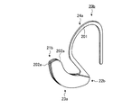
- FIG. 16 is a perspective view showing the configuration of the probe 20h according to the second embodiment.
- symbol is attached
- a probe 20h shown in FIG. 16 has a substantially flat plate shape with a uniform plate thickness, and is formed by laminating a metal plate 201f and a metal plate 202g corresponding to the metal plate 201 and the metal plate 202, respectively, in the thickness direction.
- 1 has an arc-shaped side surface at the tip, and has a first contact portion 21 in contact with the semiconductor integrated circuit 100 shown in FIG. 1 and an arc-shaped side surface on this side surface.
- the second contact portion 28 that contacts the circuit board 30, the connection portion 23 that connects the first contact portion 21 and the second contact portion 28, and the second contact portion 28, part of which forms an arc shape, And an elastic portion 24 that is elastically deformed by a load applied to the portion 21 and the second contact portion 28.
- the second contact portion 28 has a side surface 28a formed in a plane corresponding to the wall surface of the fixing member 13, and fixes the probe 20h by coming into contact with the wall surface of the fixing member 13.
- FIG. 17 is a partial cross-sectional view showing a case where the probe 20h shown in FIG. 16 is introduced into the probe unit 1 shown in FIG.
- the probe 20h held in the hole 14 of the fixing member 13 is in contact with the wall surface of the fixing member 13 at the side surface 28a also in the second contact portion 28.
- the side surface 28 a is formed along the wall surface of the fixing member 13, the protruding direction of the connection portion 23 and the first contact portion 21 from the slit 12 is adjusted by the contact of the second contact portion 28. It becomes possible.
- the side surface 28a contacting the wall surface of the fixing member 13 has a positioning effect. It can be easily disposed at a predetermined position.
- the probe 20 shown in FIG. 5 or the probes 20 a to 20 g shown in FIGS. 9 to 15 may be brought into contact with the wall surface of the fixing member 13.
- the positioning effect can be obtained by bringing the second contact portion 22 or the second contact portions 22a to 22c into contact with the wall surface of the fixing member 13.
- the semiconductor integrated circuit has been described as being a QFN having no external lead.
- the semiconductor integrated circuit 102 having a lead 103 (Quad Flat) Package: QFP).
- the contact probe and the probe unit according to the present invention are useful when electrical connection is made by connecting electrical circuit boards or the like.
- Probe unit 10 Probe holder 11 Storage part 12 Slit 13 Fixing member 14 Hole part 15 Opening part 20,20a, 20b, 20c, 20d, 20e, 20f, 20g, 20h Probe 21,21a, 21b, 21c 1st contact part 22 , 22a, 22b, 22c, 28 Second contact portion 23, 23a, 26 Connection portion 24, 24a, 25, 27, 27a, 27b Elastic portion 30 Circuit board 31, 101 Electrode 100, 102 Semiconductor integrated circuit 103 Lead 201, 201a ⁇ 201f, 202,202a ⁇ 202g Metal plate
Landscapes
- Engineering & Computer Science (AREA)
- Computer Hardware Design (AREA)
- Microelectronics & Electronic Packaging (AREA)
- Physics & Mathematics (AREA)
- General Physics & Mathematics (AREA)
- Measuring Leads Or Probes (AREA)
Abstract
L'invention concerne une sonde de contact en forme de plaque (20) en contact avec différents substrats, la sonde comprenant : une partie conductrice comportant une première section de contact (21) qui possède une surface latérale incurvée en arc à une extrémité avant, sa surface latérale étant en contact avec un substrat, une seconde section de contact (22) qui possède une surface latérale incurvée en arc, sa surface latérale étant en contact avec l'autre substrat, et une section connexion (23) qui connecte la première section de contact (21) et la seconde section de contact (22) ; et une partie élastique (24), qui est formée au moyen d'une plaque métallique (201) ayant une température maximale d'utilisation supérieure ou égale à la valeur maximale d'une température ambiante d'utilisation, qui se prolonge à partir de la seconde section de contact (22), possède une partie incurvée en arc et est déformée élastiquement par une charge appliquée sur la première section de contact (21) et la seconde section de contact (22), la partie conductrice comportant une plaque métallique (202) produite à partir d'un matériau conducteur différent de celui de la partie élastique (24).
Applications Claiming Priority (2)
| Application Number | Priority Date | Filing Date | Title |
|---|---|---|---|
| JP2010-162165 | 2010-07-16 | ||
| JP2010162165 | 2010-07-16 |
Publications (1)
| Publication Number | Publication Date |
|---|---|
| WO2012008541A1 true WO2012008541A1 (fr) | 2012-01-19 |
Family
ID=45469536
Family Applications (1)
| Application Number | Title | Priority Date | Filing Date |
|---|---|---|---|
| PCT/JP2011/066141 Ceased WO2012008541A1 (fr) | 2010-07-16 | 2011-07-14 | Sonde de contact et unité de détection |
Country Status (2)
| Country | Link |
|---|---|
| TW (1) | TW201217793A (fr) |
| WO (1) | WO2012008541A1 (fr) |
Cited By (2)
| Publication number | Priority date | Publication date | Assignee | Title |
|---|---|---|---|---|
| JP2016038206A (ja) * | 2014-08-05 | 2016-03-22 | 株式会社アイエスシーIsc Co., Ltd. | ポゴピン用プローブ部材 |
| US9726693B2 (en) | 2013-04-18 | 2017-08-08 | Isc Co., Ltd. | Probe member for pogo pin |
Families Citing this family (2)
| Publication number | Priority date | Publication date | Assignee | Title |
|---|---|---|---|---|
| CN108572264B (zh) * | 2018-06-21 | 2023-12-01 | 武汉精测电子集团股份有限公司 | 一种单缓冲通道的压接弹片 |
| CN115060930B (zh) * | 2022-05-25 | 2025-08-19 | 欧拓飞科技(珠海)有限公司 | 一种端子检测插座 |
Citations (4)
| Publication number | Priority date | Publication date | Assignee | Title |
|---|---|---|---|---|
| JPH11344508A (ja) * | 1998-06-02 | 1999-12-14 | Japan Electronic Materials Corp | プローブ及びこのプローブを用いたプローブカード |
| JP2005228496A (ja) * | 2004-02-10 | 2005-08-25 | Neomax Material:Kk | 端子用クラッド材およびその端子用クラッド材によって形成されたアルミニウム電線用端子 |
| JP2007503103A (ja) * | 2003-06-11 | 2007-02-15 | シンチ コネクターズ インコーポレーテッド | 電気コネクタ |
| JP2008309535A (ja) * | 2007-06-13 | 2008-12-25 | Japan Electronic Materials Corp | コンタクトプローブ及びその製造方法 |
-
2011
- 2011-07-14 WO PCT/JP2011/066141 patent/WO2012008541A1/fr not_active Ceased
- 2011-07-15 TW TW100125051A patent/TW201217793A/zh unknown
Patent Citations (4)
| Publication number | Priority date | Publication date | Assignee | Title |
|---|---|---|---|---|
| JPH11344508A (ja) * | 1998-06-02 | 1999-12-14 | Japan Electronic Materials Corp | プローブ及びこのプローブを用いたプローブカード |
| JP2007503103A (ja) * | 2003-06-11 | 2007-02-15 | シンチ コネクターズ インコーポレーテッド | 電気コネクタ |
| JP2005228496A (ja) * | 2004-02-10 | 2005-08-25 | Neomax Material:Kk | 端子用クラッド材およびその端子用クラッド材によって形成されたアルミニウム電線用端子 |
| JP2008309535A (ja) * | 2007-06-13 | 2008-12-25 | Japan Electronic Materials Corp | コンタクトプローブ及びその製造方法 |
Cited By (2)
| Publication number | Priority date | Publication date | Assignee | Title |
|---|---|---|---|---|
| US9726693B2 (en) | 2013-04-18 | 2017-08-08 | Isc Co., Ltd. | Probe member for pogo pin |
| JP2016038206A (ja) * | 2014-08-05 | 2016-03-22 | 株式会社アイエスシーIsc Co., Ltd. | ポゴピン用プローブ部材 |
Also Published As
| Publication number | Publication date |
|---|---|
| TW201217793A (en) | 2012-05-01 |
Similar Documents
| Publication | Publication Date | Title |
|---|---|---|
| WO2011115074A1 (fr) | Sonde de contact et unité à sonde | |
| CN111239447B (zh) | 探针、检查工具、检查单元和检查装置 | |
| JP6110086B2 (ja) | 接触検査装置 | |
| JP6103821B2 (ja) | 通電試験用プローブ | |
| CN102183680B (zh) | 连接装置 | |
| JP2017146119A (ja) | プローブピンおよびこれを用いた検査装置 | |
| CN111856090B (zh) | 探针、检查夹具及检查组件 | |
| WO2012008541A1 (fr) | Sonde de contact et unité de détection | |
| CN112345802A (zh) | 电触头及电连接装置 | |
| JP2011232313A (ja) | コンタクトプローブおよびプローブユニット | |
| CN115015602A (zh) | 探针、检查工具及检查工具单元 | |
| JP2011133354A (ja) | コンタクトプローブおよびプローブユニット | |
| JP5480717B2 (ja) | 通電検査用プローブ | |
| TW202323827A (zh) | 探針卡 | |
| JP2013148433A (ja) | コンタクトプローブおよびプローブユニット | |
| JP2013061189A (ja) | コンタクトプローブおよびプローブユニット | |
| WO2012063858A1 (fr) | Unité formant sonde | |
| JP2013061188A (ja) | コンタクトプローブおよびプローブユニット | |
| WO2024122229A1 (fr) | Sonde | |
| JP2013148432A (ja) | コンタクトプローブおよびプローブユニット | |
| WO2012118026A1 (fr) | Sonde à contact et unité de sonde | |
| CN100486046C (zh) | Ic插座 | |
| JP2020076664A (ja) | プローブピン、検査治具、検査ユニットおよび検査装置 | |
| JP2006294281A (ja) | 半導体装置の検査装置 | |
| JP2016212040A (ja) | コンタクト |
Legal Events
| Date | Code | Title | Description |
|---|---|---|---|
| 121 | Ep: the epo has been informed by wipo that ep was designated in this application |
Ref document number: 11806871 Country of ref document: EP Kind code of ref document: A1 |
|
| NENP | Non-entry into the national phase |
Ref country code: DE |
|
| 122 | Ep: pct application non-entry in european phase |
Ref document number: 11806871 Country of ref document: EP Kind code of ref document: A1 |
|
| NENP | Non-entry into the national phase |
Ref country code: JP |