WO2012008683A2 - 플렉서블 전자소자의 제조방법, 플렉서블 전자소자 및 플렉서블 기판 - Google Patents
플렉서블 전자소자의 제조방법, 플렉서블 전자소자 및 플렉서블 기판 Download PDFInfo
- Publication number
- WO2012008683A2 WO2012008683A2 PCT/KR2011/003784 KR2011003784W WO2012008683A2 WO 2012008683 A2 WO2012008683 A2 WO 2012008683A2 KR 2011003784 W KR2011003784 W KR 2011003784W WO 2012008683 A2 WO2012008683 A2 WO 2012008683A2
- Authority
- WO
- WIPO (PCT)
- Prior art keywords
- substrate
- flexible
- flexible substrate
- electronic device
- manufacturing
- Prior art date
- Legal status (The legal status is an assumption and is not a legal conclusion. Google has not performed a legal analysis and makes no representation as to the accuracy of the status listed.)
- Ceased
Links
Images

Classifications
-
- H—ELECTRICITY
- H10—SEMICONDUCTOR DEVICES; ELECTRIC SOLID-STATE DEVICES NOT OTHERWISE PROVIDED FOR
- H10K—ORGANIC ELECTRIC SOLID-STATE DEVICES
- H10K71/00—Manufacture or treatment specially adapted for the organic devices covered by this subclass
-
- H—ELECTRICITY
- H05—ELECTRIC TECHNIQUES NOT OTHERWISE PROVIDED FOR
- H05K—PRINTED CIRCUITS; CASINGS OR CONSTRUCTIONAL DETAILS OF ELECTRIC APPARATUS; MANUFACTURE OF ASSEMBLAGES OF ELECTRICAL COMPONENTS
- H05K1/00—Printed circuits
- H05K1/02—Details
- H05K1/0277—Bendability or stretchability details
-
- H—ELECTRICITY
- H05—ELECTRIC TECHNIQUES NOT OTHERWISE PROVIDED FOR
- H05K—PRINTED CIRCUITS; CASINGS OR CONSTRUCTIONAL DETAILS OF ELECTRIC APPARATUS; MANUFACTURE OF ASSEMBLAGES OF ELECTRICAL COMPONENTS
- H05K3/00—Apparatus or processes for manufacturing printed circuits
- H05K3/30—Assembling printed circuits with electric components, e.g. with resistors
- H05K3/303—Assembling printed circuits with electric components, e.g. with resistors with surface mounted components
-
- H—ELECTRICITY
- H10—SEMICONDUCTOR DEVICES; ELECTRIC SOLID-STATE DEVICES NOT OTHERWISE PROVIDED FOR
- H10D—INORGANIC ELECTRIC SEMICONDUCTOR DEVICES
- H10D30/00—Field-effect transistors [FET]
- H10D30/60—Insulated-gate field-effect transistors [IGFET]
- H10D30/67—Thin-film transistors [TFT]
- H10D30/6758—Thin-film transistors [TFT] characterised by the insulating substrates
-
- H—ELECTRICITY
- H10—SEMICONDUCTOR DEVICES; ELECTRIC SOLID-STATE DEVICES NOT OTHERWISE PROVIDED FOR
- H10D—INORGANIC ELECTRIC SEMICONDUCTOR DEVICES
- H10D86/00—Integrated devices formed in or on insulating or conducting substrates, e.g. formed in silicon-on-insulator [SOI] substrates or on stainless steel or glass substrates
- H10D86/01—Manufacture or treatment
- H10D86/021—Manufacture or treatment of multiple TFTs
- H10D86/0214—Manufacture or treatment of multiple TFTs using temporary substrates
-
- H—ELECTRICITY
- H10—SEMICONDUCTOR DEVICES; ELECTRIC SOLID-STATE DEVICES NOT OTHERWISE PROVIDED FOR
- H10D—INORGANIC ELECTRIC SEMICONDUCTOR DEVICES
- H10D86/00—Integrated devices formed in or on insulating or conducting substrates, e.g. formed in silicon-on-insulator [SOI] substrates or on stainless steel or glass substrates
- H10D86/40—Integrated devices formed in or on insulating or conducting substrates, e.g. formed in silicon-on-insulator [SOI] substrates or on stainless steel or glass substrates characterised by multiple TFTs
- H10D86/411—Integrated devices formed in or on insulating or conducting substrates, e.g. formed in silicon-on-insulator [SOI] substrates or on stainless steel or glass substrates characterised by multiple TFTs characterised by materials, geometry or structure of the substrates
-
- H—ELECTRICITY
- H10—SEMICONDUCTOR DEVICES; ELECTRIC SOLID-STATE DEVICES NOT OTHERWISE PROVIDED FOR
- H10D—INORGANIC ELECTRIC SEMICONDUCTOR DEVICES
- H10D86/00—Integrated devices formed in or on insulating or conducting substrates, e.g. formed in silicon-on-insulator [SOI] substrates or on stainless steel or glass substrates
- H10D86/40—Integrated devices formed in or on insulating or conducting substrates, e.g. formed in silicon-on-insulator [SOI] substrates or on stainless steel or glass substrates characterised by multiple TFTs
- H10D86/60—Integrated devices formed in or on insulating or conducting substrates, e.g. formed in silicon-on-insulator [SOI] substrates or on stainless steel or glass substrates characterised by multiple TFTs wherein the TFTs are in active matrices
-
- H—ELECTRICITY
- H10—SEMICONDUCTOR DEVICES; ELECTRIC SOLID-STATE DEVICES NOT OTHERWISE PROVIDED FOR
- H10K—ORGANIC ELECTRIC SOLID-STATE DEVICES
- H10K50/00—Organic light-emitting devices
- H10K50/80—Constructional details
-
- H—ELECTRICITY
- H10—SEMICONDUCTOR DEVICES; ELECTRIC SOLID-STATE DEVICES NOT OTHERWISE PROVIDED FOR
- H10K—ORGANIC ELECTRIC SOLID-STATE DEVICES
- H10K59/00—Integrated devices, or assemblies of multiple devices, comprising at least one organic light-emitting element covered by group H10K50/00
- H10K59/10—OLED displays
- H10K59/12—Active-matrix OLED [AMOLED] displays
- H10K59/1201—Manufacture or treatment
-
- H—ELECTRICITY
- H10—SEMICONDUCTOR DEVICES; ELECTRIC SOLID-STATE DEVICES NOT OTHERWISE PROVIDED FOR
- H10K—ORGANIC ELECTRIC SOLID-STATE DEVICES
- H10K71/00—Manufacture or treatment specially adapted for the organic devices covered by this subclass
- H10K71/80—Manufacture or treatment specially adapted for the organic devices covered by this subclass using temporary substrates
-
- H—ELECTRICITY
- H10—SEMICONDUCTOR DEVICES; ELECTRIC SOLID-STATE DEVICES NOT OTHERWISE PROVIDED FOR
- H10K—ORGANIC ELECTRIC SOLID-STATE DEVICES
- H10K77/00—Constructional details of devices covered by this subclass and not covered by groups H10K10/80, H10K30/80, H10K50/80 or H10K59/80
- H10K77/10—Substrates, e.g. flexible substrates
- H10K77/111—Flexible substrates
-
- H—ELECTRICITY
- H10—SEMICONDUCTOR DEVICES; ELECTRIC SOLID-STATE DEVICES NOT OTHERWISE PROVIDED FOR
- H10K—ORGANIC ELECTRIC SOLID-STATE DEVICES
- H10K2102/00—Constructional details relating to the organic devices covered by this subclass
- H10K2102/301—Details of OLEDs
- H10K2102/311—Flexible OLED
-
- H—ELECTRICITY
- H10—SEMICONDUCTOR DEVICES; ELECTRIC SOLID-STATE DEVICES NOT OTHERWISE PROVIDED FOR
- H10K—ORGANIC ELECTRIC SOLID-STATE DEVICES
- H10K59/00—Integrated devices, or assemblies of multiple devices, comprising at least one organic light-emitting element covered by group H10K50/00
- H10K59/80—Constructional details
-
- Y—GENERAL TAGGING OF NEW TECHNOLOGICAL DEVELOPMENTS; GENERAL TAGGING OF CROSS-SECTIONAL TECHNOLOGIES SPANNING OVER SEVERAL SECTIONS OF THE IPC; TECHNICAL SUBJECTS COVERED BY FORMER USPC CROSS-REFERENCE ART COLLECTIONS [XRACs] AND DIGESTS
- Y02—TECHNOLOGIES OR APPLICATIONS FOR MITIGATION OR ADAPTATION AGAINST CLIMATE CHANGE
- Y02E—REDUCTION OF GREENHOUSE GAS [GHG] EMISSIONS, RELATED TO ENERGY GENERATION, TRANSMISSION OR DISTRIBUTION
- Y02E10/00—Energy generation through renewable energy sources
- Y02E10/50—Photovoltaic [PV] energy
- Y02E10/549—Organic PV cells
-
- Y—GENERAL TAGGING OF NEW TECHNOLOGICAL DEVELOPMENTS; GENERAL TAGGING OF CROSS-SECTIONAL TECHNOLOGIES SPANNING OVER SEVERAL SECTIONS OF THE IPC; TECHNICAL SUBJECTS COVERED BY FORMER USPC CROSS-REFERENCE ART COLLECTIONS [XRACs] AND DIGESTS
- Y02—TECHNOLOGIES OR APPLICATIONS FOR MITIGATION OR ADAPTATION AGAINST CLIMATE CHANGE
- Y02P—CLIMATE CHANGE MITIGATION TECHNOLOGIES IN THE PRODUCTION OR PROCESSING OF GOODS
- Y02P70/00—Climate change mitigation technologies in the production process for final industrial or consumer products
- Y02P70/50—Manufacturing or production processes characterised by the final manufactured product
-
- Y—GENERAL TAGGING OF NEW TECHNOLOGICAL DEVELOPMENTS; GENERAL TAGGING OF CROSS-SECTIONAL TECHNOLOGIES SPANNING OVER SEVERAL SECTIONS OF THE IPC; TECHNICAL SUBJECTS COVERED BY FORMER USPC CROSS-REFERENCE ART COLLECTIONS [XRACs] AND DIGESTS
- Y10—TECHNICAL SUBJECTS COVERED BY FORMER USPC
- Y10T—TECHNICAL SUBJECTS COVERED BY FORMER US CLASSIFICATION
- Y10T29/00—Metal working
- Y10T29/49—Method of mechanical manufacture
- Y10T29/49002—Electrical device making
- Y10T29/49117—Conductor or circuit manufacturing
- Y10T29/49124—On flat or curved insulated base, e.g., printed circuit, etc.
- Y10T29/4913—Assembling to base an electrical component, e.g., capacitor, etc.
Definitions
- the present invention relates to a method for manufacturing a flexible electronic device, a flexible electronic device manufactured by the method, and a flexible substrate used in the flexible electronic device. More specifically, the present invention has a low surface roughness and a coefficient of thermal expansion. It is possible to apply a high process temperature of the glass substrate level, and to produce a flexible electronic device including a flexible substrate having a new structure with excellent handling characteristics, and to manufacture the flexible electronic device and the flexible electronic device manufactured by the method A flexible substrate for use.
- the technology disclosed in the above-mentioned patents has a processable temperature of 100 to 350 ° C. because the substrate is made of plastic. Since the process is essential, there is a problem that the device cannot be manufactured with a plastic substrate. In addition, in the manufacturing process, defects such as cracking and peeling may occur due to differences in thermal expansion coefficients between inorganic semiconductors such as Si, SiO 2 , and SiN, and insulators and plastics, which are substrates, and thus yields may be lowered.
- Korean Patent Laid-Open Publication No. 2004-0097228 discloses forming a separation layer, a thin film device, an adhesive layer, and a temporary substrate in order on a glass substrate, and then irradiating the separation layer with light such as a laser. A method of separating the glass substrate and the transfer layer is disclosed.
- a thick film metal substrate having a thickness of 15 to 150 ⁇ m used in a flexible electronic device has a surface roughness of several hundred nm or more in terms of its manufacturing method.
- the surface roughness increases proportionally as the thickness increases, so that the deposition method and conditions
- the deposition method and conditions There is a problem in manufacturing a flexible metal substrate to have a low surface roughness because it changes. Accordingly, when using a conventional metal substrate, in order to reduce the surface roughness on the metal substrate, it was essential to apply a polymer-based flattening layer on the metal substrate or perform a polishing process.
- the present invention as a means for solving the problems of the present invention, forming a flexible substrate on a mother substrate; Separating the flexible substrate from the mother substrate; And forming an electronic device on a separation surface of the flexible substrate that has been in contact with the mother substrate.
- the present invention also provides a method of forming a flexible substrate on a mother substrate; Attaching a temporary substrate having an adhesive layer formed on one surface on the flexible substrate using the adhesive layer; Separating the flexible substrate to which the temporary substrate is attached from the mother substrate; And forming an electronic device on a separation surface of the flexible substrate that has been in contact with the mother substrate.
- the manufacturing method of (2) makes it possible to use the existing glass substrate process conditions and equipment using a high temperature process of 450 ° C. or higher without the problem of bending, conveying, or aligning the flexible substrate through the use of the temporary substrate.
- a peeling layer is further formed on the said mother substrate, and a flexible substrate can be isolate
- the peeling layer Even if a thin peeling layer is added between the flexible substrate and the mother substrate, the peeling layer also exhibits a surface roughness similar to that of the mother substrate, so that the surface roughness of the separation surface of the flexible substrate can be maintained at a level similar to that of the mother substrate. In this way, when the peeling layer is added, the interfacial bonding force for separating even when the yield strength of the flexible substrate is low can be lowered, thereby preventing the flexible substrate from being damaged during the separation process.
- the release layer may be composed of a composite layer laminated in multiple layers with various materials, if necessary.
- the interfacial bonding force between the release layer and the flexible substrate may be smaller than the yield strength of the flexible substrate, and the flexible substrate may be separated from the mother substrate through a physical force.
- the surface roughness of the surface of the mother substrate on which the flexible substrate is formed can be observed in a scan range of 10 ⁇ m ⁇ 10 ⁇ m using an Atomic Force Microscope (AFM).
- AFM Atomic Force Microscope
- the thickness of the said flexible substrate is 5 micrometers-500 micrometers. If the thickness of the flexible substrate is less than 5 ⁇ m, the thickness of the flexible substrate may be so thin that the thin film may be damaged when peeled off by applying a physical force. If the thickness of the flexible substrate exceeds 500 ⁇ m, the thickness is so thick that the flexible property is deteriorated. In order to exfoliate, the thickness of the flexible substrate formed on the mother substrate is most preferably in the above range.
- the thickness of the flexible substrate including the temporary substrate is preferably 5 ⁇ m to 500 ⁇ m, for the reason that the thickness of the flexible substrate is 5 ⁇ m to 500 ⁇ m. same.
- a planarization layer may be further formed between the flexible substrate and the mother substrate.
- planarization layer used in the manufacturing method of (10) or (11) is applied to a mother substrate instead of a flexible substrate, it is not necessary to consider the fabrication temperature of the electronic device, so that a polymer material may be used, and the surface roughness of the flexible substrate may be better. It helps to keep it low.
- any material capable of maintaining a low surface roughness may be used for the planarization layer, and a copolymer including polyimide (PI) or polyimide, a copolymer including polyacrylic acid or polyacrylic acid, and polystyrene (polystyrene) or copolymers containing polystyrene, polysulfate or copolymers containing polysulfite, polyamic acid or copolymers containing polyamic acid, polyamine or polyamine It is preferable to use at least one polymer compound selected from the group consisting of a copolymer, polyvinyl alcohol (Polyvinylalcohol; PVA), polyallylamine (polyallyamine) and polyacrylic acid (polyacrylic acid).
- PI polyimide
- PVA polyvinylalcohol
- PVA polyallylamine
- polyacrylic acid polyacrylic acid
- a separation layer can be formed between the temporary substrate and the adhesive layer, to facilitate separation from the temporary substrate.
- the mother substrate can be made of glass, metal or polymer material.
- glass in the case of glass, it may include one or more glass materials selected from the group consisting of silicate glass, borosilicate glass, phosphate glass, fused silica glass, quartz, sapphire, E2K, Vycor.
- metal Fe, Ag, Au, Cu, Cr, W, Al, W, Mo, Zn, Ni, Pt, Pd, Co, In.
- metals or alloys thereof selected from the group consisting of Mn, Si, Ta, Ti, Sn, Zn, Pb, V, Ru, Ir, Zr, Rh, Mg, Invar and Stainless Use Stainless (SUS) It may include.
- the flexible substrate may be a composite structure laminated with two or more different materials.
- the adhesive layer includes at least one or more polymer adhesives selected from the group consisting of epoxy, silicone, or acrylic series, and SiO 2 , MgO, ZrO 2 , Al 2 It is preferable to include at least one material selected from the group consisting of O 3 , Ni, Al and mica, and use temperature is 450 ° C. or higher.
- the shape of the mother substrate may be a flat plate, semi-cylindrical or cylindrical, in the case of cylindrical can be used a roll to roll process to another shape It is suitable for mass production compared to its mother board.
- the thickness of the flexible substrate is preferably 5 ⁇ m to 500 ⁇ m, and the reason is as described above.
- the method of manufacturing the flexible electronic device, the flexible electronic device, and the flexible substrate according to the present invention can obtain the following effects, and are expected to contribute to manufacturing a high performance flexible electronic device at low cost.
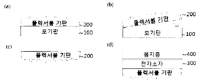
- FIG. 1 illustrates a method of manufacturing a flexible electronic device according to a first embodiment of the present invention.
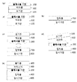
- FIG. 2 illustrates a method of manufacturing a flexible electronic device according to a second embodiment of the present invention, and a peeling mode when a peeling layer is formed between the flexible substrate and the mother substrate.
- FIG. 7 illustrates a method of manufacturing a flexible electronic device according to a third embodiment of the present invention.
- FIG 8 illustrates optical and electrical characteristics of the flexible electronic device and the electronic device formed on the glass substrate according to the third embodiment of the present invention.
- the inventors of the present invention provide a release substrate 500 formed on the mother substrate 100 and the mother substrate 100 or the flexible substrate 200. And the interfacial bonding force between the flexible substrate and the flexible substrate 200 were examined, and FIG. 4 shows the result.
- the initial applied stress was 0.03 N
- the final applied stress was 7.5 N
- the application speed was 5 N / min
- the moving speed of the probe was 10 mm / min
- the length was 15 mm.
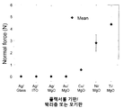
- the interfacial bonding force was smaller than the measurement range of the scratch test regardless of the material of the mother substrate or the release layer.
- Au, Cu, Ni or Ti was formed on the glass substrate after the release layer (ITO or MgO) was formed, the interfacial bonding force was measured to be smaller than the scratch test measurement range even when Au was deposited on the MgO.
- the interfacial bonding force increased to 0.56N, 2.81N, and 4.37N for Cu, Ni, and Ti, respectively, but in all cases, the flexible substrate layer was separated from the mother substrate. The interfacial bonding strength was low enough to physically separate from the layer without damaging the flexible substrate, and the actual separation surface showed similar surface roughness as the mother substrate.
- an OLED device was formed on the separation surface of the flexible substrate 200 separated from the glass substrate.
- the OLED device forms a hole injection with CuO having a thickness of 1 nm using Cu as a reflective electrode, and forms a-NPD as a hole transporting layer with a thickness of 70 nm on the hole injection layer.
- Alq3 is formed as a light emitting layer with a thickness of 40 nm
- a hole blocking layer is formed on the light emitting layer with a thickness of 5 nm
- Alq3 is formed as an electron transport layer with a thickness of 20 nm on the hole blocking layer, and 10 nm thick on the electron transport layer.
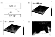
- the interface bonding force of the surface to be peeled off, the deposition conditions, the peeling method, and the material type of the flexible substrate are different, but in general, the thickness of the flexible substrate should be 5 ⁇ m or more, without damaging the flexible substrate. Separation was possible from the plates, more preferably at least 10 ⁇ m. As shown in FIG. 5D, when the Ag thickness is about 5 ⁇ m, the flexible substrate is torn during peeling and handling becomes difficult.
- a flexible substrate eg, a release layer 500 is formed between the mother substrate 100 and the flexible substrate 200. 200
- the separation form of the flexible substrate 200 may be separated at the interface of the flexible substrate 200 (FIG. 2B), or may be separated at the interface between the mother substrate 100 and the release layer 500. 2C), or may be separated from the inner surface of the release layer 500 (FIG. 2D).
- the subsequent process may not be necessary in the case of FIG. 2B, but in the case of FIGS. 2C and 2D, a process of removing the release layer 500 may be added.
- a 120 nm thick ITO layer is formed as a release layer on a glass substrate, and a 50 nm Ti layer and a 100 nm Au layer, which is a seed layer, are respectively formed as a base layer for forming a Cu layer.
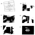
- a Ti / Au / Cu flexible substrate made of a 40 ⁇ m thick Cu layer the flexible substrate Ti / Au / Cu layer was separated from the glass substrate / ITO layer by physical separation (FIG. 6A).
- the surface roughness of the surface of the glass substrate separated from the flexible substrate was 6.4 nm (FIG. 6B).
- the surface roughness of the flexible substrate formed on the glass substrate was large as 593.2 nm (Fig. 6c), but the surface roughness of the separated surface of the flexible substrate separated from the glass substrate was 6.1 nm, which is very low surface very similar to that of the mother substrate. It was confirmed that roughness can be obtained.
- the third embodiment is different from the first embodiment in that a temporary substrate 600 for handling the flexible substrate 200 is used.
- a temporary substrate 600 for handling the flexible substrate 200 is used.
- depending on the intended use of the attached temporary substrate 600 can be used or separated in the attached state.
- separation of the temporary substrate 600 it is preferable to form a separation layer between the adhesive layer 700 and the temporary substrate 600.
- the flexible substrate Ti / Au / Cu layer including the temporary substrate layer was separated from the glass substrate / ITO layer in a physical manner without using a large force.
- a separation surface of the flexible substrate 200 having a very low surface roughness separated from the glass substrate was obtained.
- an OLED device was formed on the flexible substrate. The OLED device forms a pattern using a photoresist with 100 nm Ag as a reflective electrode on the front surface, and then forms a hole injection with CuO in a thickness of 1 nm using Ag as a flexible substrate as a reflective electrode, and has a thickness of 70 nm on the hole injection layer.
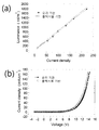
- FIG. 8 shows the results of evaluating the electro-optical characteristics of the flexible OLEDs having a light emitting area of 3 mm ⁇ 3 mm manufactured by the same process as in the third embodiment.
- the results of the current-light quantity and voltage-current characteristics are within the measurement error range. The same electrical and optical properties were shown.
Landscapes
- Engineering & Computer Science (AREA)
- Manufacturing & Machinery (AREA)
- Microelectronics & Electronic Packaging (AREA)
- Physics & Mathematics (AREA)
- Optics & Photonics (AREA)
- Electroluminescent Light Sources (AREA)
- Manufacturing Of Printed Wiring (AREA)
- Structure Of Printed Boards (AREA)
Priority Applications (4)
| Application Number | Priority Date | Filing Date | Title |
|---|---|---|---|
| JP2013519564A JP5879343B2 (ja) | 2010-07-13 | 2011-05-24 | フレキシブル電子素子の製造方法、フレキシブル電子素子及びフレキシブル基板 |
| CN201180042476.6A CN103140953B (zh) | 2010-07-13 | 2011-05-24 | 柔性电子器件、制造柔性电子器件的方法以及柔性衬底 |
| US13/809,729 US20130105203A1 (en) | 2010-07-13 | 2011-05-24 | Flexible electronic device, method for manufacturing same, and a flexible substrate |
| EP11806968.1A EP2595211A4 (de) | 2010-07-13 | 2011-05-24 | Flexible elektronische vorrichtung, herstellungsverfahren dafür und flexibles substrat |
Applications Claiming Priority (2)
| Application Number | Priority Date | Filing Date | Title |
|---|---|---|---|
| KR1020100067533A KR101147988B1 (ko) | 2010-07-13 | 2010-07-13 | 물리적 박리 방법을 이용한 플렉서블 전자소자의 제조방법, 플렉서블 전자소자 및 플렉서블 기판 |
| KR10-2010-0067533 | 2010-07-13 |
Publications (2)
| Publication Number | Publication Date |
|---|---|
| WO2012008683A2 true WO2012008683A2 (ko) | 2012-01-19 |
| WO2012008683A3 WO2012008683A3 (ko) | 2012-05-03 |
Family
ID=45469877
Family Applications (1)
| Application Number | Title | Priority Date | Filing Date |
|---|---|---|---|
| PCT/KR2011/003784 Ceased WO2012008683A2 (ko) | 2010-07-13 | 2011-05-24 | 플렉서블 전자소자의 제조방법, 플렉서블 전자소자 및 플렉서블 기판 |
Country Status (6)
| Country | Link |
|---|---|
| US (1) | US20130105203A1 (de) |
| EP (1) | EP2595211A4 (de) |
| JP (1) | JP5879343B2 (de) |
| KR (1) | KR101147988B1 (de) |
| CN (1) | CN103140953B (de) |
| WO (1) | WO2012008683A2 (de) |
Cited By (1)
| Publication number | Priority date | Publication date | Assignee | Title |
|---|---|---|---|---|
| EP2945467A4 (de) * | 2013-01-09 | 2016-09-07 | Mitsui Mining & Smelting Co | Elektrolytische kupferfolie und elektronische vorrichtung |
Families Citing this family (32)
| Publication number | Priority date | Publication date | Assignee | Title |
|---|---|---|---|---|
| JP5899220B2 (ja) * | 2010-09-29 | 2016-04-06 | ポスコ | ロール状の母基板を利用したフレキシブル電子素子の製造方法、フレキシブル電子素子及びフレキシブル基板 |
| KR101271838B1 (ko) * | 2010-11-24 | 2013-06-07 | 주식회사 포스코 | 보강기판을 이용한 플렉서블 전자소자의 제조방법, 플렉서블 전자소자 및 플렉서블 기판 |
| US8841161B2 (en) | 2012-02-05 | 2014-09-23 | GTAT.Corporation | Method for forming flexible solar cells |
| US20130200497A1 (en) * | 2012-02-05 | 2013-08-08 | Twin Creeks Technologies, Inc. | Multi-layer metal support |
| US8916954B2 (en) | 2012-02-05 | 2014-12-23 | Gtat Corporation | Multi-layer metal support |
| US8785294B2 (en) | 2012-07-26 | 2014-07-22 | Gtat Corporation | Silicon carbide lamina |
| KR102481056B1 (ko) | 2012-08-10 | 2022-12-27 | 가부시키가이샤 한도오따이 에네루기 켄큐쇼 | 반도체 장치 및 전자 장치 |
| KR102065589B1 (ko) | 2013-04-17 | 2020-01-14 | 삼성디스플레이 주식회사 | 플렉서블 디스플레이 장치의 제조방법 |
| CN103390674B (zh) * | 2013-07-17 | 2015-09-30 | 深圳先进技术研究院 | Czts柔性太阳电池及其制备方法 |
| KR101493396B1 (ko) * | 2013-07-26 | 2015-02-13 | 코닝정밀소재 주식회사 | 디스플레이 패널용 초 박판 유리 핸들링 방법 |
| KR102064277B1 (ko) * | 2013-08-12 | 2020-01-13 | 동우 화인켐 주식회사 | 플렉서블 터치 스크린 패널의 제조 방법 |
| CN104576969B (zh) * | 2013-10-11 | 2017-03-29 | 昆山工研院新型平板显示技术中心有限公司 | 一种柔性光电器件的制备方法 |
| KR102169862B1 (ko) * | 2013-12-19 | 2020-10-26 | 엘지디스플레이 주식회사 | 유기발광다이오드 표시장치 및 이의 제조방법 |
| KR101543888B1 (ko) | 2013-12-20 | 2015-08-11 | 주식회사 포스코 | 방열성이 우수한 금속 봉지재, 그 제조방법 및 상기 금속 봉지재로 봉지된 유연전자소자 |
| CN103779390B (zh) | 2014-02-11 | 2016-08-17 | 京东方科技集团股份有限公司 | 一种柔性显示基板及其制备方法 |
| US9577196B2 (en) * | 2014-02-28 | 2017-02-21 | International Business Machines Corporation | Optoelectronics integration by transfer process |
| CN104022062B (zh) | 2014-06-12 | 2016-08-17 | 京东方科技集团股份有限公司 | 一种柔性显示面板的制备方法 |
| KR102281329B1 (ko) | 2014-12-19 | 2021-07-26 | 삼성디스플레이 주식회사 | 플렉서블 디스플레이 장치 및 그 제조방법 |
| KR102303243B1 (ko) | 2015-01-14 | 2021-09-17 | 삼성디스플레이 주식회사 | 표시 장치의 제조 장치 및 표시 장치의 제조 방법 |
| KR102421579B1 (ko) * | 2015-11-16 | 2022-07-18 | 삼성디스플레이 주식회사 | 폴더블 표시 장치 |
| JP2017134329A (ja) * | 2016-01-29 | 2017-08-03 | 株式会社 オルタステクノロジー | 液晶表示装置及びその製造方法 |
| CN107102756B (zh) * | 2016-02-23 | 2021-04-06 | 群创光电股份有限公司 | 触控装置及其制造方法 |
| US10600354B2 (en) * | 2016-04-22 | 2020-03-24 | Glo Ab | Small pitch direct view display and method of making thereof |
| KR102703408B1 (ko) * | 2016-06-10 | 2024-09-09 | 삼성디스플레이 주식회사 | 표시 장치 및 그의 제조 방법 |
| CN105870327A (zh) * | 2016-06-17 | 2016-08-17 | 深圳市华星光电技术有限公司 | 柔性oled的制作方法及柔性oled |
| US10418237B2 (en) * | 2016-11-23 | 2019-09-17 | United States Of America As Represented By The Secretary Of The Air Force | Amorphous boron nitride dielectric |
| CN107222974B (zh) * | 2017-07-01 | 2019-04-12 | 华中科技大学 | 一种延性电路制作方法 |
| CN109732227B (zh) * | 2019-01-29 | 2020-11-10 | 京东方科技集团股份有限公司 | 一种柔性显示器件切割装置及切割方法 |
| KR102731215B1 (ko) * | 2019-11-04 | 2024-11-15 | 이 잉크 코포레이션 | 광 투과성 기판 및 전기영동 매체를 포함하는 3차원, 컬러-변화 오브젝트들 |
| KR20220006670A (ko) | 2020-07-08 | 2022-01-18 | 삼성디스플레이 주식회사 | 표시 장치 |
| US11889741B2 (en) | 2020-11-20 | 2024-01-30 | Samsung Display Co., Ltd. | Display panel and method of manufacturing the same |
| KR102797728B1 (ko) * | 2023-04-07 | 2025-04-23 | 국방과학연구소 | 유연 신축 소자의 제조방법 및 이에 의해 제조된 플렉서블 태양전지 |
Citations (6)
| Publication number | Priority date | Publication date | Assignee | Title |
|---|---|---|---|---|
| KR20040097228A (ko) | 1996-08-27 | 2004-11-17 | 세이코 엡슨 가부시키가이샤 | 전사 방법 및 액티브 매트릭스 기판 제조 방법 |
| KR20060134934A (ko) | 2003-11-21 | 2006-12-28 | 코닌클리즈케 필립스 일렉트로닉스 엔.브이. | 액티브 매트릭스 디스플레이 및 플라스틱 기판을 구비하는다른 전자 장치 |
| KR20080024037A (ko) | 2006-09-12 | 2008-03-17 | 엘지.필립스 엘시디 주식회사 | 평판표시소자 및 그 제조방법 |
| KR20080065210A (ko) | 2007-01-08 | 2008-07-11 | 포항공과대학교 산학협력단 | 플렉서블 소자의 제조 방법 및 플렉서블 표시 장치의 제조방법 |
| KR20090114195A (ko) | 2008-04-29 | 2009-11-03 | 삼성전자주식회사 | 가요성 표시 장치의 제조 방법 |
| KR20090123164A (ko) | 2008-05-27 | 2009-12-02 | 엘지디스플레이 주식회사 | 플렉서블 표시장치의 제조 방법 |
Family Cites Families (20)
| Publication number | Priority date | Publication date | Assignee | Title |
|---|---|---|---|---|
| US5707715A (en) * | 1996-08-29 | 1998-01-13 | L. Pierre deRochemont | Metal ceramic composites with improved interfacial properties and methods to make such composites |
| CN100421926C (zh) * | 2001-09-11 | 2008-10-01 | 美国杜邦泰津胶片合伙人有限公司 | 用于柔性电子器件和光电子器件的热稳定聚萘二甲酸乙二醇酯膜 |
| JP4267243B2 (ja) * | 2002-03-05 | 2009-05-27 | 出光興産株式会社 | 電界効果トランジスター、その製造方法及び該電界効果トランジスターを製造するための積層体 |
| JP4023285B2 (ja) * | 2002-10-24 | 2007-12-19 | ソニー株式会社 | 光・電気配線混載ハイブリッド回路基板及びその製造方法並びに光・電気配線混載ハイブリッド回路モジュール及びその製造方法 |
| JP4693411B2 (ja) * | 2002-10-30 | 2011-06-01 | 株式会社半導体エネルギー研究所 | 半導体装置の作製方法 |
| JP2004247373A (ja) * | 2003-02-12 | 2004-09-02 | Semiconductor Energy Lab Co Ltd | 半導体装置 |
| WO2005041249A2 (en) * | 2003-10-28 | 2005-05-06 | Semiconductor Energy Laboratory Co., Ltd. | Method of manufacturing optical film |
| TWI230798B (en) * | 2004-02-19 | 2005-04-11 | Univ Nat Formosa | Flexible plastic substrate for optical display and producing process |
| JP4213616B2 (ja) * | 2004-03-31 | 2009-01-21 | 大日本印刷株式会社 | 液晶パネル用ベースフィルム、液晶パネル用機能フィルム、機能フィルムの製造方法、および機能フィルムの製造装置 |
| JP2006236626A (ja) * | 2005-02-22 | 2006-09-07 | Shinshu Univ | 電極層付き可撓性樹脂フィルムの製造方法 |
| KR20080023612A (ko) * | 2006-09-11 | 2008-03-14 | 엘지.필립스 엘시디 주식회사 | 평판 표시 소자 및 그 제조방법 |
| US8168511B2 (en) * | 2007-09-20 | 2012-05-01 | Sharp Kabushiki Kaisha | Display device manufacturing method and laminated structure |
| CN101244428A (zh) * | 2008-02-18 | 2008-08-20 | 宁波永正精密不锈钢有限公司 | 亮面精密不锈钢带生产方法 |
| KR100947435B1 (ko) * | 2008-03-25 | 2010-03-12 | 삼성모바일디스플레이주식회사 | 플렉서블 디스플레이 및 그 제조 방법 |
| US8182633B2 (en) * | 2008-04-29 | 2012-05-22 | Samsung Electronics Co., Ltd. | Method of fabricating a flexible display device |
| KR101540163B1 (ko) * | 2008-05-16 | 2015-07-28 | 신닛테츠스미킹 마테리알즈 가부시키가이샤 | 가요성 디스플레이용 스테인리스 강박 |
| TWI354854B (en) * | 2008-09-15 | 2011-12-21 | Ind Tech Res Inst | Substrate structures applied in flexible electrica |
| BRPI0923756A2 (pt) * | 2008-12-31 | 2016-01-19 | 3M Innovative Properties Co | método para produção de um componente de um dispositivo, e os componentes e dispositivos resultantes |
| JP5292217B2 (ja) * | 2009-08-04 | 2013-09-18 | 株式会社半導体エネルギー研究所 | 半導体装置の作製方法及び電子書籍の作製方法 |
| KR101063361B1 (ko) * | 2010-05-06 | 2011-09-07 | 포항공과대학교 산학협력단 | 플렉서블 전자소자의 제조방법, 플렉서블 전자소자 및 플렉서블 기판 |
-
2010
- 2010-07-13 KR KR1020100067533A patent/KR101147988B1/ko not_active Expired - Fee Related
-
2011
- 2011-05-24 EP EP11806968.1A patent/EP2595211A4/de not_active Withdrawn
- 2011-05-24 JP JP2013519564A patent/JP5879343B2/ja not_active Expired - Fee Related
- 2011-05-24 CN CN201180042476.6A patent/CN103140953B/zh not_active Expired - Fee Related
- 2011-05-24 WO PCT/KR2011/003784 patent/WO2012008683A2/ko not_active Ceased
- 2011-05-24 US US13/809,729 patent/US20130105203A1/en not_active Abandoned
Patent Citations (6)
| Publication number | Priority date | Publication date | Assignee | Title |
|---|---|---|---|---|
| KR20040097228A (ko) | 1996-08-27 | 2004-11-17 | 세이코 엡슨 가부시키가이샤 | 전사 방법 및 액티브 매트릭스 기판 제조 방법 |
| KR20060134934A (ko) | 2003-11-21 | 2006-12-28 | 코닌클리즈케 필립스 일렉트로닉스 엔.브이. | 액티브 매트릭스 디스플레이 및 플라스틱 기판을 구비하는다른 전자 장치 |
| KR20080024037A (ko) | 2006-09-12 | 2008-03-17 | 엘지.필립스 엘시디 주식회사 | 평판표시소자 및 그 제조방법 |
| KR20080065210A (ko) | 2007-01-08 | 2008-07-11 | 포항공과대학교 산학협력단 | 플렉서블 소자의 제조 방법 및 플렉서블 표시 장치의 제조방법 |
| KR20090114195A (ko) | 2008-04-29 | 2009-11-03 | 삼성전자주식회사 | 가요성 표시 장치의 제조 방법 |
| KR20090123164A (ko) | 2008-05-27 | 2009-12-02 | 엘지디스플레이 주식회사 | 플렉서블 표시장치의 제조 방법 |
Non-Patent Citations (1)
| Title |
|---|
| See also references of EP2595211A4 |
Cited By (1)
| Publication number | Priority date | Publication date | Assignee | Title |
|---|---|---|---|---|
| EP2945467A4 (de) * | 2013-01-09 | 2016-09-07 | Mitsui Mining & Smelting Co | Elektrolytische kupferfolie und elektronische vorrichtung |
Also Published As
| Publication number | Publication date |
|---|---|
| EP2595211A4 (de) | 2014-07-16 |
| JP5879343B2 (ja) | 2016-03-08 |
| KR101147988B1 (ko) | 2012-05-24 |
| CN103140953B (zh) | 2016-08-03 |
| CN103140953A (zh) | 2013-06-05 |
| KR20120006844A (ko) | 2012-01-19 |
| US20130105203A1 (en) | 2013-05-02 |
| WO2012008683A3 (ko) | 2012-05-03 |
| JP2013546156A (ja) | 2013-12-26 |
| EP2595211A2 (de) | 2013-05-22 |
Similar Documents
| Publication | Publication Date | Title |
|---|---|---|
| WO2012008683A2 (ko) | 플렉서블 전자소자의 제조방법, 플렉서블 전자소자 및 플렉서블 기판 | |
| WO2012043971A2 (ko) | 롤 형상의 모기판을 이용한 플렉서블 전자소자의 제조방법, 플렉서블 전자소자 및 플렉서블 기판 | |
| KR101063361B1 (ko) | 플렉서블 전자소자의 제조방법, 플렉서블 전자소자 및 플렉서블 기판 | |
| US7575983B2 (en) | Method for fabricating a device with flexible substrate and method for stripping flexible-substrate | |
| TWI778019B (zh) | 併入積層基板的電子組件及其製造方法 | |
| KR101508544B1 (ko) | 플렉서블 표시장치의 제조 방법 | |
| KR101555551B1 (ko) | 플렉시블 표시장치 제조방법 | |
| TW200525270A (en) | Active matrix displays and other electronic devices having plastic substrates | |
| WO2013062246A1 (ko) | 그라핀층을 포함하는 가스 배리어 필름, 이를 포함하는 플렉시블 기판 및 그 제조방법 | |
| WO2016106797A1 (zh) | 一种柔性有机发光显示器及其制作方法 | |
| KR101328275B1 (ko) | 화학적 박리 방법을 이용한 플렉서블 전자소자의 제조방법, 플렉서블 전자소자 및 플렉서블 기판 | |
| WO2020040518A1 (ko) | 투명 발광소자 디스플레이용 매립형 전극 기판 및 이의 제조방법 | |
| TWI703477B (zh) | 薄膜觸控感測器及其製造方法 | |
| WO2011162461A1 (ko) | 투명 전극 및 이의 제조 방법 | |
| TW201818552A (zh) | 薄膜電晶體的製備方法 | |
| WO2013168968A1 (ko) | 금속 산화물/질화물/황화물 박막의 전사 방법 및 이에 사용되는 전사용 시트 | |
| KR101845440B1 (ko) | 플렉서블 표시장치의 제조 방법 | |
| KR101476746B1 (ko) | 내부식성 모기판을 이용한 플렉서블 금속 기판과 전자소자의 제조방법, 플렉서블 전자소자 및 플렉서블 금속 기판 | |
| KR101493396B1 (ko) | 디스플레이 패널용 초 박판 유리 핸들링 방법 | |
| KR20180039999A (ko) | 2차원 나노박막을 전사시키는 방법 | |
| CN104009065A (zh) | 面板结构及其制造方法 | |
| WO2017074049A1 (ko) | 투광성 기판의 제조방법 및 이를 통해 제조된 투광성 기판 | |
| TW201635119A (zh) | 薄膜觸控感測器及其製造方法 | |
| KR20170121372A (ko) | 실링 라인을 이용한 플렉서블 금속 필름의 제조 방법 | |
| Chen et al. | P‐168: Development of Conformal Anti‐diffraction Transparent LTPS TFT Pixel Arrays on Two‐axis Surface |
Legal Events
| Date | Code | Title | Description |
|---|---|---|---|
| WWE | Wipo information: entry into national phase |
Ref document number: 201180042476.6 Country of ref document: CN |
|
| 121 | Ep: the epo has been informed by wipo that ep was designated in this application |
Ref document number: 11806968 Country of ref document: EP Kind code of ref document: A2 |
|
| ENP | Entry into the national phase |
Ref document number: 2013519564 Country of ref document: JP Kind code of ref document: A |
|
| WWE | Wipo information: entry into national phase |
Ref document number: 13809729 Country of ref document: US |
|
| NENP | Non-entry into the national phase |
Ref country code: DE |
|
| WWE | Wipo information: entry into national phase |
Ref document number: 2011806968 Country of ref document: EP |