WO2012014529A1 - Dispositif d'éclairage et dispositif d'affichage - Google Patents
Dispositif d'éclairage et dispositif d'affichage Download PDFInfo
- Publication number
- WO2012014529A1 WO2012014529A1 PCT/JP2011/058196 JP2011058196W WO2012014529A1 WO 2012014529 A1 WO2012014529 A1 WO 2012014529A1 JP 2011058196 W JP2011058196 W JP 2011058196W WO 2012014529 A1 WO2012014529 A1 WO 2012014529A1
- Authority
- WO
- WIPO (PCT)
- Prior art keywords
- light
- light emitting
- guide plate
- light guide
- emitting diodes
- Prior art date
- Legal status (The legal status is an assumption and is not a legal conclusion. Google has not performed a legal analysis and makes no representation as to the accuracy of the status listed.)
- Ceased
Links
Images






Classifications
-
- G—PHYSICS
- G02—OPTICS
- G02B—OPTICAL ELEMENTS, SYSTEMS OR APPARATUS
- G02B6/00—Light guides; Structural details of arrangements comprising light guides and other optical elements, e.g. couplings
- G02B6/0001—Light guides; Structural details of arrangements comprising light guides and other optical elements, e.g. couplings specially adapted for lighting devices or systems
- G02B6/0011—Light guides; Structural details of arrangements comprising light guides and other optical elements, e.g. couplings specially adapted for lighting devices or systems the light guides being planar or of plate-like form
- G02B6/0033—Means for improving the coupling-out of light from the light guide
- G02B6/0035—Means for improving the coupling-out of light from the light guide provided on the surface of the light guide or in the bulk of it
- G02B6/0038—Linear indentations or grooves, e.g. arc-shaped grooves or meandering grooves, extending over the full length or width of the light guide
-
- G—PHYSICS
- G02—OPTICS
- G02B—OPTICAL ELEMENTS, SYSTEMS OR APPARATUS
- G02B6/00—Light guides; Structural details of arrangements comprising light guides and other optical elements, e.g. couplings
- G02B6/0001—Light guides; Structural details of arrangements comprising light guides and other optical elements, e.g. couplings specially adapted for lighting devices or systems
- G02B6/0011—Light guides; Structural details of arrangements comprising light guides and other optical elements, e.g. couplings specially adapted for lighting devices or systems the light guides being planar or of plate-like form
- G02B6/0075—Arrangements of multiple light guides
- G02B6/0076—Stacked arrangements of multiple light guides of the same or different cross-sectional area
Definitions
- the present invention relates to an illuminating device, and more particularly to an illuminating device including a light source and a light guide plate that emits light from the light source to an irradiated object such as a liquid crystal panel, and a display device using the illuminating device.
- liquid crystal display devices have been widely used in liquid crystal televisions, monitors, mobile phones and the like as flat panel displays having features such as thinness and light weight compared to conventional cathode ray tubes.
- a liquid crystal display device includes an illumination device (backlight device) that emits light, and a liquid crystal panel that displays a desired image by serving as a shutter for light from a light source provided in the illumination device. It is included.
- liquid crystal display device as described above, a plurality of display areas are provided on the display surface of the liquid crystal panel, and in the illumination device, a plurality of light emitting areas in which light from the light source is incident on the plurality of display areas, respectively Set.
- low power consumption has been achieved by performing local dimming (area active backlight) driving in which the light source is driven to light in units of light emitting areas.
- the same number of first light guide members as the number of light emitting areas installed are provided, so that when the plurality of light emitting areas are provided, the number of parts of the lighting device increases. There was a problem that the cost could not be suppressed and the cost increased.
- the first and second light guides are provided when a plurality of light emitting areas are provided. There has been a problem in that cost is increased because much time and labor are required for connecting the members.
- an object of the present invention is to provide an illumination device that can suppress an increase in the number of parts even when a plurality of light emitting areas are provided, and a display device using the illumination device.
- an illumination device includes a light source and a light guide plate that guides light from the light source in a predetermined propagation direction and emits the light to an object to be irradiated. Because The light guide plate is provided with a plurality of light guide plate members stacked in a predetermined direction, Each of the plurality of light guide plate members is provided with a light blocking portion so that a plurality of light emitting areas that respectively emit light from the plurality of light sources are formed on a light emitting surface of the light guide plate. It is what.
- the light guide plate of the lighting device configured as described above is provided with a plurality of light guide plate members stacked in a predetermined direction.
- Each of the plurality of light guide plate members is provided with a light blocking portion so that a plurality of light emitting areas for emitting light from the plurality of light sources are formed on the light emitting surface of the light guide plate.
- the illumination device as the light blocking portion, a slit provided in the light guide plate member along a boundary line of the plurality of light emitting areas, and a facing surface side of the light guide plate member facing the light emitting surface It is preferable that a reflective member provided in the is used.
- a reflective material that reflects light is installed inside the slit.
- a light scattering portion that scatters light from the light source is provided on the facing surface side facing the light emitting surface according to the light emitting area. It is preferable.
- the light scattering portion can efficiently emit light from the corresponding light emitting area from the corresponding light emitting area, and the luminance of the light emitting area can be easily increased.
- each of the plurality of light guide plate members is provided with a plurality of light incident surfaces on which light from a plurality of light sources respectively enter linearly.
- a compact lighting device can be easily configured even when the number of light emitting areas is increased.
- the light guide plate may be provided between a plurality of light incident surfaces provided on the plurality of light guide plate members and a plurality of light sources that respectively input light to the plurality of light incident surfaces. It is preferable that a partition member for restricting the emission direction of the light from the plurality of light sources is attached so that the light from the plurality of light sources enters only the corresponding light incident surface.
- the display device of the present invention is characterized by using any one of the above lighting devices.
- a display unit that displays information is used as the irradiated object. It is preferable that the display unit includes a plurality of display areas into which light from the plurality of light emitting areas is incident.
- the light source of the corresponding light emitting area is appropriately driven to be turned on, and a display device with reduced power consumption can be easily configured.
- the present invention even when a plurality of light emitting areas are provided, it is possible to suppress an increase in the number of parts, and it is possible to provide a lighting device that is inexpensive and a display device using the lighting device.
- FIG. 1 is a diagram for explaining an illumination device and a liquid crystal display device according to a first embodiment of the present invention.
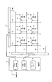
- FIG. 2 is a diagram for explaining the configuration of the liquid crystal panel shown in FIG.
- FIG. 3 is a block diagram illustrating a configuration example of the panel control unit illustrated in FIG. 2.
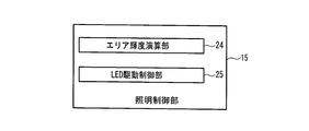
- 4 is a block diagram illustrating a configuration example of the illumination control unit illustrated in FIG.
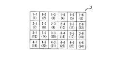
- FIG. 5 is a diagram illustrating a specific example of a plurality of light emitting areas provided in the lighting device illustrated in FIG. 1 and a plurality of display areas irradiated with light from these light emitting areas.
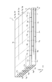
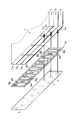
- FIG. 6 is a perspective view illustrating a configuration example of the light guide plate illustrated in FIG. 1.
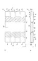
- FIG. 7A and 7B are a plan view and a side view of the first light guide plate member shown in FIG. 6, respectively.
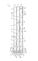
- 8A and 8B are a plan view and a side view of the second light guide plate member shown in FIG. 6, respectively.
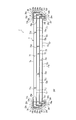
- FIG. 9A and FIG. 9B are a plan view and a side view of the third light guide plate member shown in FIG. 6, respectively.
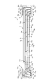
- FIG. 10 is a diagram for explaining a main configuration of the illumination device shown in FIG.
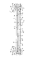
- FIG. 11 is a diagram illustrating an operation example of the illumination device illustrated in FIG. 1.
- FIG. 12 is a diagram for explaining a main configuration of a modified example of the illumination device shown in FIG.
- FIG. 13 is a diagram for explaining a main configuration of an illumination device according to the second embodiment of the present invention.
- FIG. 10 is a diagram for explaining a main configuration of the illumination device shown in FIG.
- FIG. 11 is a diagram illustrating an operation example of the illumination device illustrated in FIG. 1.
- FIG. 12 is a
- FIG. 14 is a diagram for explaining a main configuration of an illumination apparatus according to the third embodiment of the present invention.
- FIG. 15 is a perspective view illustrating a configuration example of the partition member illustrated in FIG. 14.
- FIG. 16 is a diagram for explaining a main configuration of an illuminating device according to the fourth embodiment of the present invention.
- FIG. 17 is a diagram for explaining a main configuration of an illumination apparatus according to the fifth embodiment of the present invention.
- FIG. 1 is a diagram for explaining an illumination device and a liquid crystal display device according to a first embodiment of the present invention.
- the illuminating device 2 of this invention and the liquid crystal panel 3 as a display part which displays the information while irradiating the light from the illuminating device 2 are provided.
- the illumination device 2 and the liquid crystal panel 3 are integrated as a transmissive liquid crystal display device 1.
- the lighting device 2 includes a plurality of light emitting diodes (LEDs) 4 as light sources, an LED substrate 5 on which the plurality of light emitting diodes 4 are mounted, a frame body 6 to which the LED substrate 5 is attached, and the light emitting diodes 4. And a light guide plate 7 for emitting the light to the liquid crystal panel 3 as an irradiated object. Moreover, in this illuminating device 2, the light emission surface 7a of the light-guide plate 7 is formed with the some light emission area which each light-emits the light from the some light emitting diode 4 so that it may explain in full detail later.
- LEDs light emitting diodes
- liquid crystal display device 1 of the present embodiment light from a plurality of light emitting areas is incident on a plurality of display areas provided in the liquid crystal panel 3, and the light emitting diodes 4 are provided in units of light emitting areas. Local dimming (area active backlight) driving for lighting is performed.
- the light guide plate 7 is provided with a plurality of, for example, three light guide plate members, that is, first, second, and third light guide plate members 71, 72, 73. These first, second, and third light guide plate members 71, 72, 73 are arranged in a predetermined direction so that the light emitting surface of the first light guide plate member 71 constitutes the light emitting surface 7 a of the light guide plate 7.
- the light emitting diodes 4 are laminated so that light from the plurality of light emitting diodes 4 is appropriately guided to emit light from the corresponding light emitting areas (details will be described later).
- red, green, and blue light emitting diodes that emit red (R), green (G), and blue (B) light, respectively, are integrated with each of the plurality of light emitting diodes 4.
- the so-called three-in-one (3 in 1) type is used.
- 24 light-emitting areas set for each light-emitting diode 4 are determined and set on the display surface of the liquid crystal panel 3 corresponding to these light-emitting areas. The light from the corresponding light emitting diodes 4 is made incident on the 24 display areas.
- each of the light emitting areas uses the 3in1 light emitting diode 4, a light source of a plurality of colors that can be mixed with white is used in each light emitting area.
- a polarizing sheet 8 and a prism (light collecting) sheet 9 are installed between the illumination device 2 and the liquid crystal panel 3, and the illumination from the illumination device 2 is performed by these optical sheets.
- the display performance of the liquid crystal panel 3 is improved by appropriately increasing the brightness of light.
- liquid crystal display device 1 signal lines (source lines) and control lines (gate lines), which will be described later, included in the liquid crystal panel 3 are connected to a drive control circuit 11 via an FPC (Flexible Printed Circuit) 9. Yes.
- the drive control circuit 11 performs drive control on a pixel basis for a plurality of pixels provided in the liquid crystal panel 3.
- a lighting drive circuit 12 that drives the plurality of light emitting diodes 4 to light is installed in the vicinity of the drive control circuit 11.
- the lighting drive circuit 12 is configured to drive each of the light emitting diodes 4 using, for example, PWM dimming.
- FIG. 2 is a diagram for explaining the configuration of the liquid crystal panel shown in FIG.
- FIG. 3 is a block diagram illustrating a configuration example of the panel control unit illustrated in FIG. 2.
- 4 is a block diagram illustrating a configuration example of the illumination control unit illustrated in FIG.
- an image signal is input to the control unit 13 from the outside of the liquid crystal display device 1 via a signal source (not shown) such as a TV (receiver) or a PC.
- the control unit 13 is provided in the drive control circuit 11 (FIG. 1), and substantially performs drive control of the liquid crystal panel 3 using the input image signal. Furthermore, the control unit 13 is configured to substantially perform drive control of the illumination device 2 using the input image signal.
- control unit 13 uses the image signal to control the liquid crystal panel 3 in units of pixels, the panel control unit 14 as a display control unit, and the image signal to each of the lighting devices 2.
- An illumination control unit 15 that controls driving of the light emitting diode 4 and a frame memory 16 configured to be able to store display data in units of frames included in the image signal are provided.
- an ASIC Application ⁇ ⁇ Specific Integrated Circuit
- predetermined calculation processing can be performed at high speed.
- the panel control unit 14 and the illumination control unit 15 are provided as described above, in the liquid crystal display device 1 of the present embodiment, the panel control unit 14 and the illumination control unit 15 are each a liquid crystal panel (display unit). 3 and the illumination device 2 can be appropriately driven, and high-quality display can be easily performed.
- the panel control unit 14 outputs each instruction signal to the source driver 17 and the gate driver 18. Further, in the panel control unit 14, the luminance value of each light emitting area is notified from an area luminance calculation unit (described later) provided in the illumination control unit 15, and an instruction signal to the source driver 17 is notified. After being corrected to a signal reflecting the luminance value of each light emitting area, it is output from the panel control unit 14 to the source driver 17 (details will be described later).
- the source driver 17 and the gate driver 18 are drive circuits that drive a plurality of pixels P provided in the liquid crystal panel 3 in units of pixels.
- the source driver 17 and the gate driver 18 include a plurality of signal lines S1 to SM (M Is an integer of 2 or more) and a plurality of control lines G1 to GN (N is an integer of 2 or more).
- the signal lines S1 to SM and the control lines G1 to GN are arranged in a matrix, and the areas of the plurality of pixels P are formed in the areas partitioned in the matrix.
- the liquid crystal panel 3 is not provided with a color filter.
- the RGB light-emitting diodes provided for each light-emitting area are sequentially turned on, so that each pixel P has a red color. , Green and blue pixels.
- each control line G1 to GN is provided for each pixel P, and connected to the gate of the switching element 19 using, for example, a thin film transistor (Thin Film Transistor).
- the source of the switching element 19 is connected to each of the signal lines S1 to SM.
- a pixel electrode 20 provided for each pixel P is connected to the drain of each switching element 19.
- the common electrode 21 is configured to face the pixel electrode 20 with a liquid crystal layer (not shown) provided on the liquid crystal panel 3 interposed therebetween.
- the panel control unit 14 is also provided with an image processing unit 22 and a display data correction calculation unit 23 with reference to FIG. 3.
- the source driver 17 and the gate driver 18 are used by using the input image signal.
- Each instruction signal is generated. That is, the image processing unit 22 generates an instruction signal for the gate driver 18 based on the display data of the image signal stored in the frame memory 16 and outputs the instruction signal to the gate driver 18. Thereby, the gate driver 18 sequentially outputs gate signals for turning on the gates of the corresponding switching elements 19 to the control lines G1 to GN based on the instruction signal from the image processing unit 22. Further, the image processing unit 22 generates an instruction signal to the source driver 17 based on the display data and outputs the instruction signal to the display data correction calculation unit 23.
- the display data correction calculation unit 23 receives not only an instruction signal from the image processing unit 22 to the source driver 17 but also the luminance value of each light emitting area from the area luminance calculation unit.
- the luminance value of each light emitting area is a luminance value after being corrected using the luminance value of the surrounding light emitting area, and is a value that takes into account the influence of light crosstalk from the surrounding light emitting area. Then, as will be described in detail later, the display data correction calculation unit 23 corrects the instruction signal to the source driver 17 pixel by pixel using the luminance value of each light emitting area, and generates a new instruction signal. To the source driver 17.
- the source driver 17 generates a voltage signal (gradation voltage) for designating the luminance (gradation) of the information displayed on the display surface based on the instruction signal from the display data correction calculation unit 23 as the signal line S1. Output as appropriate to SM.
- the display data correction calculation unit 23 acquires the display data of the image signal directly from the frame memory 16 and uses the corrected luminance value of the corresponding light emitting area for each pixel P. Alternatively, the acquired display data may be corrected.
- the illumination control unit 15 is provided with an area luminance calculation unit 24 and an LED drive control unit 25 with reference to FIG.
- the area luminance calculation unit 24 acquires luminance information of the pixels P included in the corresponding display area for each light emitting area from the input image signal.
- the area luminance calculation unit 24 uses the acquired luminance information of the pixel P to perform luminance calculation processing that is obtained by calculating the luminance value of each color of red, green, and blue in each light emitting area. (Details will be described later).
- the area luminance calculation unit 24 performs an area crosstalk correction process, which will be described later, on the luminance value of each color obtained by performing the luminance calculation process, thereby affecting the influence of light crosstalk from surrounding light emitting areas. Thus, the corrected luminance value of each color is obtained. Then, the area luminance calculation unit 24 outputs the calculated luminance value of each color after correction of each light emitting area to the display data correction calculation unit 23 and the LED drive control unit 25.
- the light emitting area and the display area respectively provided on the lighting device 2 side and the liquid crystal panel 3 side, and the luminance calculation processing and area crosstalk correction processing in the area luminance calculation unit 24 are specifically described. I will explain it.
- FIG. 5 is a diagram for explaining a specific example of a plurality of light emitting areas provided in the illumination device shown in FIG. 1 and a plurality of display areas irradiated with light from these light emitting areas.
- a plurality of light emitting areas and a plurality of display areas will be described.
- a total of 24 light emitting areas 1-1, 1-2,..., 4-5, 4-6 are arranged opposite to the liquid crystal panel 3 side to provide planar illumination light.
- These light emitting areas 1-1, 1-2,..., 4-5, 4-6 are provided in the first, second, and third light guide plate members 71, 72, 73 as will be described in detail later.
- the light blocking section described later emits light from the corresponding light emitting diode 4.
- the light emitting areas 1-1, 1-2,..., 4-5, 4-6 are shown separated from each other by vertical and horizontal lines in order to clearly show them. Actually, the light emitting areas 1-1, 1-2,..., 4-5, 4-6 are not separated from one another by a boundary line or the like installed on the light emitting surface 7 a.
- each of these display areas (1), (2),..., (23), (24) includes a plurality of pixels P. Specifically, when, for example, 1920 ⁇ 1080 pixels P are provided in the horizontal and vertical directions in the liquid crystal panel 3, the display areas (1), (2),..., (23), (24 ) Includes 320 ⁇ 270 pixels P.
- the matrix-shaped light emitting areas 1-1, 1-2,..., 4-5, 4-6 and the matrix-shaped display areas (1), (2),. , (23), and (24) are set in a one-to-one relationship, and the local light is appropriately irradiated to one display area according to information to be displayed by illumination light from one light emitting area. Dimming driving is performed.
- each of the light emitting areas 1-1, 1-2,..., 4-5, 4-6 the RGB colors from the RGB light emitting diodes included in the corresponding light emitting diode 4 are displayed.
- Each color light can be independently emitted to the liquid crystal panel 3 side.
- -1, 1-2,..., 4-5, 4-6 can be appropriately incident, and the reproducibility of each color of RGB can be easily improved.
- the area luminance calculation unit 24 9 corresponding to the light emitting areas 1-2, 1-3, 1-4, 2-2, 2-3, 2-4, 3-2, 3-3, and 3-4, respectively.
- luminance calculation processing is performed for each of the display areas (2), (3), (4), (8), (9), (10), (14), (15), and (16). Accordingly, red, blue, and green in the corresponding light emitting areas 1-2, 1-3, 1-4, 2-2, 2-3, 2-4, 3-2, 3-3, 3-4 The luminance value of each color is obtained.
- the area luminance calculation unit 24 acquires luminance information of a plurality of pixels P (for example, 320 ⁇ 270 pixels P) included in the display area (2) from the frame memory 16. Then, the area luminance calculation unit 24 performs luminance calculation processing on the acquired luminance information to extract, for example, data of the maximum luminance value for each of red, blue, and green colors, and displays the display area (2 ) Corresponding to the luminance values of the respective colors in the light emitting area 1-2. That is, when the area luminance calculation unit 24 executes the luminance calculation process, the luminance value of the pixel P to be displayed in red with the highest luminance is emitted from the plurality of pixels P included in the display area (2). It is selected as the red luminance value in area 1-2.
- the area luminance calculation unit 24 can prevent the luminance value from being extracted as the maximum luminance value when there is a pixel P having an abnormally high luminance value compared to the surrounding pixels P due to noise mixing. It is configured as follows.
- the luminance value of the pixel P to be displayed in green with the highest luminance is selected as the green luminance value in the light emitting area 1-2.
- the luminance value of the pixel P to be displayed in blue with the highest luminance is selected as the blue luminance value in the light emitting area 1-2.
- the area luminance calculation unit 24 determines the luminance values of the selected red, blue, and green colors as the luminance values of the light emitting area 1-2.
- the area luminance calculation unit 24 performs red, blue in the light emitting areas 1-3, 1-4, 2-2, 2-3, 2-4, 3-2, 3-3, 3-4. The luminance value of each color of green and green is obtained. Then, the area luminance calculation unit 24 sets the luminance value of the light emitting area 2-3 for each of the red, blue, and green colors, the surrounding light emitting areas 1-2, 1-3, 1-4, and 2-2. Area crosstalk correction processing using luminance values 2-4, 3-2, 3-3, and 3-4 is performed.
- the area luminance calculation unit 24 corrects the obtained luminance value by using a correction coefficient stored in a memory (not shown), thereby red, blue, and green colors. In addition, the brightness value after correction of each illumination area is calculated.
- the light from the surrounding light emitting areas 1-2, 1-3, 1-4, 2-2, 2-4, 3-2, 3-3, 3-4 is used.
- a correction coefficient that cancels out the luminance increase in each of the red, blue, and green colors is obtained in advance and stored in the memory.
- the area luminance calculation unit 24 corrects each color of the light emitting area 2-3 by using the luminance value of each color of the light emitting area 2-3 obtained by the luminance calculation processing and the correction coefficient held in the memory. Later luminance values are calculated.
- the area luminance calculation unit 24 outputs the calculated luminance value of each color after correction of each illumination area to the display data correction calculation unit 23 and the LED drive control unit 25.
- the internal structure of the liquid crystal panel 3 and optical sheets such as the light guide plate 7, the polarizing sheet 8, and the prism sheet 9 are used. Therefore, it is possible to more reliably eliminate the influence of crosstalk in the liquid crystal display device 1 and to improve display quality more easily.
- the LED drive control unit 25 constitutes a drive control unit that drives the light source to turn on, and responds based on the corrected luminance value of each of the plurality of illumination areas from the area luminance calculation unit 24.
- the lighting periods of the RGB light emitting diodes are determined, and the light emitting diodes of the respective RGB colors are driven to light by PWM dimming according to the determined lighting periods. That is, the LED drive control unit 25 determines the on / off duty in the PWM dimming according to the luminance value determined by the area luminance calculation unit 24, and a signal that indicates the determined on / off duty. Is output to the lighting drive circuit 12 (FIG. 1) as an instruction signal. Then, the lighting drive circuit 12 drives each of the light emitting diodes by supplying power to the RGB light emitting diodes based on the instruction signal.
- the display data correction calculation unit 23 the luminance value of each color of red, green, and blue in each of the light emitting areas 1-1, 1-2,. When transmitted, these luminance values are used to correct the instruction signal to the source driver 17 input from the image processing unit 22 and output to the source driver 17 as a new instruction signal. That is, the display data correction calculation unit 23 corresponds to the corresponding color from the area luminance calculation unit 24 with respect to the gradation voltages in red, green, and blue pixel units determined by the image processing unit 22 according to the image signal. Is corrected based on the luminance value of, to obtain a new gradation voltage. Then, the display data correction calculation unit 23 generates an instruction signal instructing new gradation voltages in red, green, and blue pixel units, and outputs the instruction signal to the source driver 17.
- the panel control unit 14 uses the corrected luminance values of the plurality of light emitting areas 1-1, 1-2,..., 4-5, 4-6.
- the image signal is corrected, and drive control of the liquid crystal panel 3 is performed on a pixel basis based on the corrected image signal.
- FIG. 6 is a perspective view showing a configuration example of the light guide plate shown in FIG. 7A and 7B are a plan view and a side view of the first light guide plate member shown in FIG. 6, respectively.
- 8A and 8B are a plan view and a side view of the second light guide plate member shown in FIG. 6, respectively.
- FIG. 9A and FIG. 9B are a plan view and a side view of the third light guide plate member shown in FIG. 6, respectively.
- FIG. 10 is a diagram for explaining a main configuration of the illumination device shown in FIG.
- FIG. 11 is a diagram illustrating an operation example of the illumination device illustrated in FIG. 1.
- first to third light guide plate members 71, 72, 73 are arranged along the Z direction (predetermined direction, a direction perpendicular to the display surface of the liquid crystal panel 3). Are stacked. That is, in these first to third light guide plate members 71, 72, 73, the first light guide plate member 71 is installed on the liquid crystal panel 3 side, and as described above, the first light guide plate member 71 The light emitting surfaces are laminated in the predetermined direction so that the light emitting surface 7a of the light guide plate 7 is formed.
- each of the light guide plate members 71 to 73 for example, a transparent synthetic resin material having a plate thickness of about 1 mm to several mm is used.
- each of the light guide plate members 71 to 73 is provided with a light blocking section, and the 24 light emitting areas 1-1, 1-2,... That emit light from the 24 light emitting diodes 4 respectively. 4-5 and 4-6 are formed on the light emitting surface 7a of the light guide plate 7 as indicated by the dotted lines in FIG.
- the first light guide plate member 71 is opposed to the light emitting surface 71A constituting the light emitting surface 7a of the light guide plate 7 and the light emitting surface 71A.
- the opposed surface 71B is provided between the light emitting surface 71A and the opposed surface 71B, and includes side surfaces 71C and 71D on which the four light emitting diodes 4 are arranged to face each other. That is, on the side surface 71C, four light incident surfaces 71a on which the four light emitting diodes 4 are respectively incident are linearly provided. In addition, on the side surface 71D, four light incident surfaces 71b on which the four light emitting diodes 4 are respectively incident are provided linearly. On each of these light incident surfaces 71a and 71b, light from the light emitting diodes 4 other than the corresponding (opposing) light emitting diodes 4 is prevented from entering by a partition plate described later (details will be described later).
- the first light guide plate member 71 includes slits 71c and 71d parallel to the Y direction (vertical direction of the liquid crystal panel 3) and slits 71e, 71f and 71g parallel to the X direction (lateral direction of the liquid crystal panel 3). Is provided.
- the slits 71c to 71g are provided in the first light guide plate member 71 so as to be formed on the boundary line of the light emitting area. That is, the slit 71 c is provided from the left edge (side surface 71 ⁇ / b> C) of the first light guide plate member 71 at a position that is 1/6 of the dimension in the X direction of the first light guide plate member 71.
- the slit 71d is provided from the right edge (side surface 71D) of the first light guide plate member 71 at a position that is 1/6 of the dimension in the X direction of the first light guide plate member 71.
- the slits 71e, 71f, 71g are respectively provided at three locations that divide the dimension of the first light guide plate member 71 in the Y direction into four equal parts.
- each of the slits 71c to 71g is formed to have a bottom and an opening on the light emitting surface 71A side and the opposing surface 71B side, respectively.
- the respective opening dimensions in the Z direction are set to dimensions that leave the plate thickness (the dimension in the Z direction) of the first light guide plate member 71 about 0.5 mm to 1.0 mm. Yes.
- the opening dimensions in the X direction of the slits 71c and 71d and the opening dimensions in the Y direction of the slits 71e to 71g are set to, for example, about several mm.
- Each of the slits 71c to 71g blocks the light that has traveled.
- the slit 71c enters the inside of the first light guide plate member 71 from the lower left light incident surface 71a of FIG. The light is blocked from traveling to the right side of the slit 71c. Further, the slit 71e enters the first light guide plate member 71 from, for example, the lower left light incident surface 71a of FIG. 7A, and the light travels upward in the Y direction. Proceeding to the upper side of the slit 71e is blocked. Further, each of the slits 71c to 71g passes through the second light guide plate member 72 from the third light guide plate member 73 and the light that has entered the first light guide plate member 71 from the second light guide plate member 72. Thus, light that has entered the inside of the first light guide plate member 71 is also blocked.
- a reflection sheet 71h as a reflection member is provided on the opposing surface 71B from the side surface 71C to the slit 71c, and further, a reflection sheet 71i as a reflection member is from the side surface 71D to the slit 71d. Is provided on the opposite surface 71B.
- These reflection sheets 71h and 71i are used as the light blocking section together with the slits 71c to 71g. That is, the reflection sheets 71h and 71i reflect the light incident on the inside of the first light guide plate member 71 from the light incident surfaces 71a and 71b, respectively, so that each of these lights is the second light guide plate member 72. Blocks going to the side.
- the slits 71c to 71g and the reflection sheets 71h and 71i are used as light blocking portions. Therefore, in the first light guide plate member 71, a total of eight light emitting areas 1 are provided. -1, 2-1, 3-1, 4-1, 1-6, 2-6, 3-6, 4-6 (FIG. 5) are formed.
- scattering dot patterns 71j and 71k as light scattering portions that scatter light from the light emitting diodes 4 are provided on the facing surface 71B side according to the light emitting area.
- the scattered dot pattern 71j is opposed to the light emitting areas 1-1, 2-1, 3-1, 4-1 as indicated by the hatched portion on the left side of FIG. It is formed on the surface 71B and scatters light from the four light emitting diodes 4 to emit light from the light emitting areas 1-1, 2-1, 3-1, 4-1 respectively. .
- the scattered dot pattern 71k is a surface of the opposing surface 71B corresponding to the light emitting areas 1-6, 2-6, 3-6, 4-6, as indicated by the hatched portion on the right side of FIG.
- the light is emitted from the light emitting areas 1-6, 2-6, 3-6, and 4-6 by scattering the light from the four light emitting diodes 4 respectively.
- the second light guide plate member 72 includes a light emitting surface 72A installed in parallel to the light emitting surface 7a of the light guide plate 7, and a facing surface facing the light emitting surface 72A. It is provided between the surface 72B and the light emitting surface 72A and the opposing surface 72B, and includes side surfaces 72C and 72D on which the four light emitting diodes 4 are arranged to face each other. That is, on the side surface 72C, four light incident surfaces 72a on which the four light emitting diodes 4 are respectively incident are provided linearly. In addition, on the side surface 72D, four light incident surfaces 72b on which the four light emitting diodes 4 are respectively incident are linearly provided. In each of these light incident surfaces 72a and 72b, light from the light emitting diodes 4 other than the corresponding (opposing) light emitting diodes 4 is prevented from entering by a partition plate described later (details will be described later).
- the second light guide plate member 72 includes slits 72c and 72d parallel to the Y direction (vertical direction of the liquid crystal panel 3) and slits 72e, 72f and 72g parallel to the X direction (lateral direction of the liquid crystal panel 3). Is provided.
- the slits 72c to 72g are provided in the second light guide plate member 72 so as to be formed on the boundary line of the light emitting area. In other words, the slit 72 c is provided from the left edge (side surface 72 ⁇ / b> C) of the second light guide plate member 72 at a location 2/6 of the dimension in the X direction of the second light guide plate member 72.
- the slit 72d is provided from the right edge (side surface 72D) of the second light guide plate member 72 at a position 2/6 of the dimension in the X direction of the second light guide plate member 72.
- the slits 72e, 72f, and 72g are respectively provided at three locations that divide the dimension of the second light guide plate member 72 in the Y direction into four equal parts.
- each of the slits 72c to 72g is formed to have a bottom and an opening on the light emitting surface 72A side and the opposing surface 72B side, respectively.
- the respective opening dimensions in the Z direction are set to dimensions that leave the thickness (dimension in the Z direction) of the second light guide plate member 72 about 0.5 mm to 1.0 mm. Yes.
- the respective opening dimensions in the X direction of the slits 72c and 72d and the respective opening dimensions in the Y direction of the slits 72e to 72g are set to, for example, about several mm.
- Each of the slits 72c to 72g blocks the light that has traveled.
- the slit 72c is incident on the inside of the second light guide plate member 72 from the lower left light incident surface 72a of FIG. 8A and travels to the right in the X direction. The light is blocked from traveling to the right side of the slit 72c.
- the slit 72e enters the inside of the second light guide plate member 72 from the lower left light incident surface 72a in FIG. 8A, and the light travels upward in the Y direction. Proceeding to the upper side of the slit 72e is blocked.
- each of the slits 72c to 72g blocks light that has entered the second light guide plate member 72 from the third light guide plate member 73.
- a reflection sheet 72h as a reflection member is provided on the opposing surface 72B from the side surface 72C to the slit 72c, and further, a reflection sheet 72i as a reflection member is from the side surface 72D to the slit 72d. Is provided on the opposite surface 72B.
- These reflection sheets 72h and 72i are used as the light blocking section together with the slits 72c to 72g. That is, the reflection sheets 72h and 72i reflect the light incident on the inside of the second light guide plate member 72 from the light incident surfaces 72a and 72b, respectively, so that each of these lights is the third light guide plate member 73. Blocks going to the side.
- the slits 72c to 72g and the reflection sheets 72h and 72i are used as light blocking portions. Therefore, in the second light guide plate member 72, a total of eight light emitting areas 1 are provided. -2, 2-2, 3-2, 4-2, 1-5, 2-5, 3-5, 4-5 (FIG. 5).
- scattering dot patterns 72j and 72k as light scattering portions for scattering light from the light emitting diodes 4 are provided on the facing surface 72B side according to the light emitting area. More specifically, the scattered dot pattern 72j corresponds to the light emitting areas 1-2, 2-2, 3-2, and 4-2 as shown by the hatched portion on the left side of FIG. It is formed on the surface of the surface 72B. That is, the scattering dot pattern 72j is formed on the surface of the facing surface 72B from the straight line portion 72E directly below the slit 71c of the first light guide plate member 71 to the slit 72c.
- the scattering dot pattern 72j includes four light emitting diodes 4. Are scattered from the light emitting areas 1-2, 2-2, 3-2 and 4-2, respectively.
- the scattered dot pattern 72k is a surface of the facing surface 72B corresponding to the light emitting areas 1-5, 2-5, 3-5, 4-5, as indicated by the hatched portion on the right side of FIG. Formed on top. That is, the scattering dot pattern 72k is formed on the surface of the facing surface 72B from the straight portion 72F directly below the slit 71d of the first light guide plate member 71 to the slit 72d.
- the scattering dot pattern 72k includes four light emitting diodes 4. Are scattered from the light emitting areas 1-5, 2-5, 3-5, and 4-5, respectively.
- the third light guide plate member 73 includes a light emitting surface 73A installed in parallel to the light emitting surface 7a of the light guide plate 7, and a facing surface facing the light emitting surface 73A.
- the surface 73B is provided between the light emitting surface 73A and the opposing surface 73B, and includes side surfaces 73C and 73D on which the four light emitting diodes 4 are arranged to face each other. That is, the side surface 73C is provided with four light incident surfaces 73a on which the four light emitting diodes 4 are respectively incident.
- four light incident surfaces 73b on which the four light emitting diodes 4 are respectively incident are provided linearly. On each of these light incident surfaces 73a and 73b, light from the light emitting diodes 4 other than the corresponding (opposing) light emitting diodes 4 is prevented from entering by a partition plate described later (details will be described later).
- the third light guide plate member 73 has slits 73c parallel to the Y direction (vertical direction of the liquid crystal panel 3) and slits 73d, 73e, and 73f parallel to the X direction (lateral direction of the liquid crystal panel 3). Is provided.
- the slits 72c to 73f are provided in the third light guide plate member 73 so as to be formed on the boundary line of the light emitting area.
- the slit 73 c is provided from the left edge (side surface 73 ⁇ / b> C) of the third light guide plate member 73 at a position that is 3/6 of the dimension in the X direction of the third light guide plate member 73.
- the slits 73d, 73e, and 73f are respectively provided at three locations that divide the dimension of the third light guide plate member 73 in the Y direction into four equal parts.
- each of the slits 73c to 73f is formed to have a bottom and an opening on the light emitting surface 73A side and the opposing surface 73B side, respectively.
- the respective opening dimensions in the Z direction are set to dimensions that leave the thickness (dimension in the Z direction) of the third light guide plate member 73 about 0.5 mm to 1.0 mm. Yes.
- the opening dimension in the X direction of the slit 73c and each opening dimension in the Y direction of the slits 73d to 73f are set to about several mm, for example.
- Each of the slits 73c to 73f blocks the light that has traveled.
- the slit 73c is incident on the inside of the third light guide plate member 73 from the lower left light incident surface 73a in FIG. 9A and travels to the right in the X direction. The light is blocked from traveling to the right side of the slit 73c.
- the slit 73d enters the inside of the third light guide plate member 73 from the lower left light incident surface 73a of FIG. 9A, and the light travels upward in the Y direction. Proceeding to the upper side of the slit 73d is blocked.
- the reflection sheet 73g as a reflection member is provided on the facing surface 73B from the side surface 73C to the slit 73c, and further, the reflection sheet 73h as a reflection member is from the side surface 73D to the slit 73d. Is provided on the opposite surface 73B.
- These reflection sheets 73g and 73h are used as the light blocking section together with the slits 73c to 73f. That is, the reflection sheets 73g and 73h reflect the light incident on the inside of the third light guide plate member 73 from the light incident surfaces 73a and 73b, respectively, so that each of these lights is the third light guide plate member 73. Blocks going outside.
- the third light guide plate member 73 As described above, in the third light guide plate member 73, the slits 73c to 73f and the reflection sheets 73g and 73h are used as the light blocking portions. Therefore, the third light guide plate member 73 has a total of eight light emitting areas 1. -3, 2-3, 3-3, 4-3, 1-4, 2-4, 3-4, 4-4 (FIG. 5).
- the scattered dot pattern 73i is opposed to the light emitting areas 1-3, 2-3, 3-3, and 4-3, as indicated by the hatched portion on the left side of FIG. It is formed on the surface of the surface 73B. That is, the scattering dot pattern 73i is formed on the surface of the facing surface 73B from the straight line portion 73E directly below the slit 72c of the second light guide plate member 72 to the slit 73c.
- the scattering dot pattern 73i scatters light from the four light emitting diodes 4 to emit light from the light emitting areas 1-3, 2-3, 3-3, and 4-3, respectively.
- the scattered dot pattern 73j is a surface of the facing surface 73B corresponding to the light emitting areas 1-4, 2-4, 3-4, and 4-4, as indicated by the hatched portion on the right side of FIG. Formed on top. That is, the scattering dot pattern 73j is formed on the surface of the facing surface 73B from the straight portion 73F that is directly below the slit 72d of the second light guide plate member 72 to the slit 73d. Further, in the first and second light guide plate members 71 and 72 facing the scattering dot pattern 73j, as shown in FIG. 7B and FIG. 8B, a reflection sheet is not formed, The scattering dot pattern 73j scatters light from the four light emitting diodes 4 to emit light from the light emitting areas 1-4, 2-4, 3-4, and 4-4, respectively.
- the frame 6 is attached so that the both-sides part of the light-guide plate 7 may be covered.
- the frame 6 supports the LED substrate 5 on which twelve light emitting diodes 4 are mounted inside each side surface portion of the light guide plate 7. Further, in the LED substrate 5 on the left side of FIG. 10, the four light emitting diodes 4 are arranged in a direction perpendicular to the drawing so as to face the four light incident surfaces 71a.
- this LED board 5 arranges in the direction perpendicular
- the four light emitting diodes 4 are arranged in a direction perpendicular to the drawing so as to face the four light incident surfaces 71b. Further, in this LED substrate 5, the four light emitting diodes 4 are arranged in a direction perpendicular to the drawing so as to face the four light incident surfaces 72b, respectively, and the four light emitting diodes 4 have four light incidents. They are arranged in a direction perpendicular to the drawing so as to face the surface 73b.
- the frame 6 is provided with partition plates 6a, 6b, 6c, 6d, 6e, 6f, and 6g so that light from the light emitting diodes 4 enters only the corresponding (opposing) light incident surfaces. ing. That is, the partition plates 6a and 6b are provided so as to sandwich the four light emitting diodes 4 facing the four light incident surfaces 71a or 71b, respectively. Further, a partition plate 6e is provided between the partition plates 6a and 6b so as to partition each installation region of the four light emitting diodes 4 arranged in the direction perpendicular to the drawing.
- the three partition plates 6e are provided so as to be arranged in a straight line with the slits 71e, 71f, 71g, respectively, and four light incidents together with the partition plates 6a, 6b.
- the surfaces 71a are separated from each other.
- the partition plates 6b and 6c are provided so as to sandwich the four light emitting diodes 4 facing the four light incident surfaces 72a or 72b, respectively. Further, a partition plate 6f is provided between the partition plates 6b and 6c so as to partition each installation region of the four light emitting diodes 4 arranged in the direction perpendicular to the drawing. That is, on each side surface side of the light guide plate 7, the three partition plates 6f are provided so as to be arranged in a straight line with the slits 72e, 72f, 72g, respectively, and four light incidents together with the partition plates 6b, 6c. The surfaces 72a are separated from each other.
- partition plates 6c and 6d are provided so as to sandwich the four light emitting diodes 4 respectively facing the four light incident surfaces 73a or 73b.
- a partition plate 6g is provided between the partition plates 6c and 6d so as to partition each installation region of the four light emitting diodes 4 arranged in the direction perpendicular to the drawing. That is, on each side surface side of the light guide plate 7, three partition plates 6 g are provided so as to be aligned with the slits 73 d, 73 e, 73 f, respectively, and four light incidents together with the partition plates 6 c, 6 d.
- the surfaces 73a are separated from each other.
- the partition plates 6a to 6g are made of, for example, a metal material having a high light reflectivity.
- the light from the light-emitting diode 4 is efficiently incident on the light incident surface, thereby improving the use efficiency of the light. It can be improved.
- the light from the light emitting diode 4 facing the light incident surface 71 a is reflected by the reflection sheet 71 h and the first
- the inside of the light guide plate member 71 proceeds to the left side of FIG.
- the light is blocked by the slit 71c and scattered by the scattering dot pattern 71j, and is emitted, for example, as light from the light emitting area 1-1 to the liquid crystal panel 3 side.
- the light from the light emitting diode 4 facing the light incident surface 72a travels to the left in FIG. 11 through the second light guide plate member 72 while being reflected by the reflection sheets 71h and 72h.
- the light is blocked by the slit 72c and scattered by the scattering dot pattern 72j, and is emitted, for example, as light from the light emitting area 1-2 to the liquid crystal panel 3 side.
- the light from the light emitting diode 4 facing the light incident surface 73a travels to the left side of FIG. 11 through the inside of the third light guide plate member 73 while being reflected by the reflection sheets 72h and 73g.
- the light is blocked by the slit 73c and scattered by the scattering dot pattern 73i, and is emitted, for example, as light from the light emitting area 1-3 to the liquid crystal panel 3 side.
- the light guide plate 7 is provided with first to third light guide plate members 71 to 73 stacked in a predetermined direction. Further, the first light guide plate member 71 has eight light emitting areas 1-1, 2-1, 3-1, 4-1, 1 that emit light from eight light emitting diodes (light sources) 4, respectively. Slits 71c to 71g and reflection sheets 71h and 71i (light blocking portions) are provided so that ⁇ 6, 2-6, 3-6, and 4-6 are formed on the light emitting surface 7a of the light guide plate 7. .
- the second light guide plate member 72 has eight light emitting areas 1-2, 2-2, 3-2, 4-2, 1 for emitting light from the eight light emitting diodes (light sources) 4, respectively.
- Slits 72c to 72g and reflection sheets 72h and 72i (light blocking portions) are provided so that ⁇ 5, 2-5, 3-5, and 4-5 are formed on the light emitting surface 7a of the light guide plate 7.
- the third light guide plate member 73 has eight light emitting areas 1-3, 2-3, 3-3, 4-3, 1 that emit light from the eight light emitting diodes (light sources) 4, respectively.
- the illuminating device 2 of this embodiment unlike the said prior art example, even when providing a several light emission area, it is not necessary to provide the same number of light-guide plate members as a light emission area. As a result, in the present embodiment, unlike the conventional example, even when a plurality of light emitting areas are provided, an increase in the number of parts can be suppressed, and the illuminating device 2 can be configured at a low cost.
- the first to third light guide plate members 71 to 73 are scattered dot patterns 71j, 71k, 72j, 72k, 73i, 73j (which scatter light from the light emitting diode 4). .., 4-5, 4-6 are provided on the facing surfaces 71B to 73B facing the light-emitting surface 7a according to the light-emitting areas 1-1, 1-2,.
- the light from the light emitting diode 4 can be efficiently emitted from the corresponding light emitting areas 1-1, 1-2,..., 4-5, 4-6. It is possible to easily increase the luminance of the light emitting areas 1-1, 1-2,..., 4-5, 4-6.
- the liquid crystal display device 1 can be easily configured at a low cost, in which an increase in the number of components is suppressed.
- (1), (2), ..., (23), (24) are provided.
- the display areas (1), (2),..., (23), (24 corresponding to the display contents of the liquid crystal panel 3, the corresponding light emitting areas 1-1, 1-2, .., 4-5 and 4-6 are appropriately driven to light, and a liquid crystal display device with reduced power consumption can be easily configured.
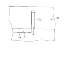
- FIG. 12 is a diagram for explaining a main configuration of a modified example of the illumination device shown in FIG.
- the main difference between the present modification and the first embodiment is that a reflecting material that reflects light is provided inside the slit.
- a reflecting material that reflects light is provided inside the slit.
- symbol is attached
- the reflective material H is installed inside the slit 71c.
- the reflecting material H for example, a white reflecting material or a specular reflecting material is used to reflect light.
- each opening dimension in the X direction and Y direction of the slit 71c is the thickness dimension of the reflective material H + ⁇ (for example, about 0.1 mm to 1 mm). ) Is set.
- FIG. 13 is a diagram for explaining a main configuration of an illumination device according to the second embodiment of the present invention.
- the main difference between the present embodiment and the first embodiment is that a separately provided LED substrate is used according to the light guide plate member.
- symbol is attached
- the LED substrate 27 provided separately is used according to the first to third light guide plate members 71 to 73.
- the frame body 28 is attached so as to cover both side portions of the light guide plate 7. Further, the frame body 28 supports the three LED substrates 27 on which the four light emitting diodes 4 are mounted inside each side surface portion of the light guide plate 7. That is, on the first LED substrate 27 from the left side of FIG. 13, the four light emitting diodes 4 are arranged in a direction perpendicular to the drawing so as to face the four light incident surfaces 71a.
- the four light emitting diodes 4 are arranged in a direction perpendicular to the drawing so as to face the four light incident surfaces 72a, respectively, and from the left side of FIG.
- the four light emitting diodes 4 are arranged in a direction perpendicular to the drawing so as to face the four light incident surfaces 73a.
- the four light emitting diodes 4 are arranged in a direction perpendicular to the drawing so as to face the four light incident surfaces 71b.
- the four light emitting diodes 4 are arranged in the direction perpendicular to the drawing so as to face the four light incident surfaces 72b, respectively, and from the right side of FIG.
- the four light emitting diodes 4 are arranged in a direction perpendicular to the drawing so as to face the four light incident surfaces 73b.
- the partition plate 29 a, 29 b, 29 c, 29 d, 29 e, 29 f, 29 g, 29 h so that the light from the light emitting diode 4 enters only the corresponding (opposing) light incident surface.
- 29i, 29j, 29k, 29l, and 29m are provided. That is, the partition plates 29a to 29e are provided so as to sandwich the four light emitting diodes 4 facing the four light incident surfaces 71a or 71b, respectively.
- a partition plate 29k is provided between the partition plates 29a to 29e so as to partition each installation region of the four light emitting diodes 4 arranged in the direction perpendicular to the drawing.
- the three partition plates 29k are provided so as to be arranged in a straight line with the slits 71e, 71f, 71g, respectively, and four light incidents together with the partition plates 29a to 29e.
- the surfaces 71a are separated from each other.
- partition plates 29d to 29h are provided so as to sandwich the four light emitting diodes 4 facing the four light incident surfaces 72a or 72b, respectively.
- a partition plate 29l is provided between the partition plates 29d to 29h so as to partition each installation region of the four light emitting diodes 4 arranged in the direction perpendicular to the drawing. That is, on each side surface side of the light guide plate 7, three partition plates 29l are provided so as to be arranged in a straight line with the slits 72e, 72f, 72g, respectively, and four light incidents together with the partition plates 29d to 29h.
- the surfaces 72a are separated from each other.
- partition plates 29g to 29j are provided so as to sandwich the four light emitting diodes 4 respectively facing the four light incident surfaces 73a or 73b. Further, a partition plate 29m is provided between the partition plates 29g to 29j so as to partition each installation region of the four light emitting diodes 4 arranged in the direction perpendicular to the drawing. That is, on each side surface side of the light guide plate 7, the three partition plates 29m are provided so as to be arranged in a straight line with the slits 73d, 73e, 73f, and four light incidents together with the partition plates 29g to 29j. The surfaces 73a are separated from each other.
- the partition plates 29a to 29m are made of, for example, a metal material having a high light reflectivity.
- the light from the light emitting diode 4 is efficiently incident on the light incident surface, and the light use efficiency is increased. It can be improved.
- the present embodiment can achieve the same operations and effects as the first embodiment. Further, in the present embodiment, since the LED substrate 27 provided separately according to the first to third light guide plate members 71 to 73 is used, each of the light incident surfaces 71a to 73a and 71b to 73b is used. Even when the light emitting portion of the light emitting diode 4 is larger than the dimension in the plate thickness direction (Z direction), it is easy for the light from the light emitting diode 4 to enter only the corresponding (opposing) light incident surface. Therefore, it is possible to easily prevent light from the plurality of light emitting diodes (light sources) 4 from being mixed with each other.
- FIG. 14 is a diagram for explaining a main configuration of an illumination apparatus according to the third embodiment of the present invention.
- FIG. 15 is a perspective view illustrating a configuration example of the partition member illustrated in FIG. 14.
- the direction of light emission from the plurality of light emitting diodes is set so that the light from the plurality of light emitting diodes enters only the corresponding light incident surface between the light emitting diodes that respectively enter light on the light surface. It is the point which attached the partition member to restrict
- symbol is attached
- the partition member 30 is attached to the both side surfaces of the light guide plate 7 inside the frame body 6. Moreover, unlike the thing of 1st Embodiment, only the partition plates 6a and 6d are provided in the inside of the frame 6. FIG. In other words, in the illumination device 2 of the present embodiment, the partition member 30 is configured to function as the partition plates 6b, 6c, 6e, 6f, and 6g.
- Each of the surfaces 71a, 72a, and 73a is provided between twelve light emitting diodes 4 that receive light.
- the partition member 30 limits the emission direction of the light from the 12 light emitting diodes 4 so that the light from the 12 light emitting diodes 4 enters only the corresponding light incident surfaces 71a, 72a, 73a. It is configured.
- the partition member 30 limits the emission direction of the light from the twelve light emitting diodes 4 so that the light from the twelve light emitting diodes 4 enters only the corresponding light incident surfaces 71b, 72b, and 73b. It is configured.
- the partition member 30 has four openings 30a, 30b, and 30c, respectively, and a member body in which a total of twelve openings 30a to 30c are formed. 30d is provided.
- the openings 30a to 30c are provided in the member main body 30d according to the position of the light emitting diode 4 mounted on the LED substrate 5, and the openings 30a to 30c are light emitting diodes as indicated by arrows in the figure. 4 is incident on the light incident surfaces 71a to 73a.
- the partition portion 30e is between two adjacent openings, that is, between the openings 30a and 30b, between the openings 30b and 30c, and the opening 30c. 30a.
- the light from the 12 light emitting diodes 4 is configured to enter only the corresponding light incident surfaces 71a, 72a, 73a.
- the present embodiment can achieve the same operations and effects as the first embodiment. Moreover, in this embodiment, since the partition member 30 is attached with respect to the light-guide plate 7, it can prevent easily that the light from the several light emitting diode (light source) 4 mutually mixes.
- FIG. 16 is a diagram for explaining a main configuration of an illuminating device according to the fourth embodiment of the present invention.
- the main difference between this embodiment and the first embodiment is that each light guide plate member is provided so that the light incident surface and the light emitting surface are parallel to each other.
- symbol is attached
- the frame 31 is attached so that the both-sides part of the light-guide plate 7 may be covered.
- the frame 31 supports the LED substrate 5 on which twelve light emitting diodes 4 are mounted inside each side surface portion of the light guide plate 7.
- the light incident surfaces 71a to 73a and 71b to 73b of the first to third light guide plate members 71 to 73 are provided so as to be parallel to the light emitting surface 7a.
- the LED board 5 is attached to the frame 31 so that it may become mutually parallel with the light emission surface 7a.
- the four light emitting diodes 4 are arranged in a direction perpendicular to the drawing so as to face the four light incident surfaces 71a. Moreover, in this LED board 5, it arranges in the direction perpendicular
- the four light emitting diodes 4 are arranged in a direction perpendicular to the drawing so as to face the four light incident surfaces 71b. Further, in this LED substrate 5, the four light emitting diodes 4 are arranged in a direction perpendicular to the drawing so as to face the four light incident surfaces 72b, respectively, and the four light emitting diodes 4 have four light incidents. They are arranged in a direction perpendicular to the drawing so as to face the surface 73b.
- 31i, 31j, and 31k are provided. That is, the partition plates 31a to 31e are provided so as to sandwich the four light emitting diodes 4 respectively facing the four light incident surfaces 71a or 71b. Further, a partition plate 31i is provided between the partition plates 31a to 31e so as to partition each installation region of the four light emitting diodes 4 arranged in a direction perpendicular to the drawing.
- the three partition plates 31i are provided so as to be arranged in a straight line with the slits 71e, 71f, 71g, respectively, and four light incidents together with the partition plates 31a to 31e.
- the surfaces 71a are separated from each other.
- the partition plates 31d to 31g are provided so as to sandwich the four light emitting diodes 4 respectively facing the four light incident surfaces 72a or 72b. Further, a partition plate 31j is provided between the partition plates 31d to 31g so as to partition each installation region of the four light emitting diodes 4 arranged in the direction perpendicular to the drawing. That is, on each side surface side of the light guide plate 7, the three partition plates 31j are provided so as to be arranged in a straight line with the slits 72e, 72f, 72g, respectively, and four light incidents together with the partition plates 31d to 31g. The surfaces 72a are separated from each other.
- partition plates 31f to 31h are provided so as to sandwich the four light emitting diodes 4 respectively facing the four light incident surfaces 73a or 73b.
- a partition plate 31k is provided between the partition plates 31f to 31h so as to partition each installation region of the four light emitting diodes 4 arranged in the direction perpendicular to the drawing. That is, on each side surface side of the light guide plate 7, the three partition plates 31k are provided so as to be arranged in a straight line with the slits 73d, 73e, 73f, respectively, and four light incidents together with the partition plates 31f to 31h.
- the surfaces 73a are separated from each other.
- the partition plates 31a to 31k are made of, for example, a metal material having a high light reflectivity.
- the light from the light-emitting diode 4 is efficiently incident on the light incident surface, and the use efficiency of the light is increased. It can be improved.
- the present embodiment can achieve the same operations and effects as the first embodiment.
- FIG. 17 is a diagram for explaining a main configuration of an illumination apparatus according to the fifth embodiment of the present invention.
- the main difference between the present embodiment and the fourth embodiment is that an LED substrate provided separately is used according to the light guide plate member.
- symbol is attached
- LED substrates 27 that are separately provided according to the first to third light guide plate members 71 to 73 are used.
- the frame body 32 is attached so as to cover both side portions of the light guide plate 7.
- the frame 32 supports the three LED substrates 27 on which the four light emitting diodes 4 are mounted inside the side surfaces of the light guide plate 7. That is, in the first LED substrate 27 from the left side of FIG. 17, the four light emitting diodes 4 are arranged in a direction perpendicular to the drawing so as to face the four light incident surfaces 71a. Further, in the second LED substrate 27 from the left side of FIG.
- the four light emitting diodes 4 are arranged in the direction perpendicular to the drawing so as to face the four light incident surfaces 72a, respectively, and from the left side of FIG.
- the four light emitting diodes 4 are arranged in a direction perpendicular to the drawing so as to face the four light incident surfaces 73a.
- the second LED board 27 from the left side of FIG. 17 is installed on the first LED board 27 from the left side of FIG. 17, and the third LED board 27 from the left side of FIG. It is installed on the second LED board 27.
- the second and third LED substrates 27 from the left side of FIG. 17 are held by the frame body 32 via the first LED substrate 27 from the left side of FIG.
- the four light emitting diodes 4 are arranged in a direction perpendicular to the drawing so as to face the four light incident surfaces 71b.
- the four light emitting diodes 4 are arranged in the direction perpendicular to the drawing so as to face the four light incident surfaces 72b, respectively, and from the right side of FIG.
- the four light emitting diodes 4 are arranged in a direction perpendicular to the drawing so as to face the four light incident surfaces 73b.
- the second LED board 27 from the right side of FIG. 17 is installed on the first LED board 27 from the right side of FIG. 17, and the third LED board 27 from the right side of FIG. It is installed on the second LED board 27.
- the second and third LED substrates 27 from the right side of FIG. 17 are held by the frame body 32 via the first LED substrate 27 from the right side of FIG.
- the light incident surfaces 71a to 73a and 71b to 73b of the first to third light guide plate members 71 to 73 are at a predetermined angle (for example, 45) with respect to the light emitting surface 7a. Degree).
- the partition plates 32a, 32b, 32c, 32d, 32e, 32f, 32g, 32h, and the like so that the light from the light emitting diode 4 enters only the corresponding (opposing) light incident surface. 32i is provided. That is, the partition plates 32a, 32b, and 32d are provided so as to sandwich the four light emitting diodes 4 facing the four light incident surfaces 71a or 71b, respectively. Further, a partition plate 32g is provided between the partition plates 32a, 32b, and 32d so as to partition each installation region of the four light emitting diodes 4 arranged in the direction perpendicular to the drawing.
- the three partition plates 32 g are provided so as to be aligned with the slits 71 e, 71 f, 71 g, respectively, and together with the partition plates 32 a, 32 b, 32 d, The light incident surfaces 71a are partitioned from each other.
- partition plates 32c, 32d, and 32f are provided so as to sandwich the four light emitting diodes 4 facing the four light incident surfaces 72a or 72b, respectively.
- a partition plate 32h is provided between the partition plates 32c, 32d, and 32f so as to partition each installation region of the four light emitting diodes 4 arranged in a direction perpendicular to the drawing. That is, on each side surface side of the light guide plate 7, the three partition plates 32h are provided so as to be arranged in a straight line with the slits 72e, 72f, 72g, respectively, and four partition plates 32c, 32d, 32f are provided.
- the light incident surfaces 72a are partitioned from each other.
- partition plates 32e and 32f are provided so as to sandwich the four light emitting diodes 4 facing the four light incident surfaces 73a or 73b, respectively.
- a partition plate 32i is provided between the partition plates 32e and 32f so as to partition each installation region of the four light emitting diodes 4 arranged in the direction perpendicular to the drawing. That is, on each side surface side of the light guide plate 7, the three partition plates 32i are provided so as to be arranged in a straight line with the slits 73d, 73e, 73f, respectively, and four light incidents together with the partition plates 32e, 32f.
- the surfaces 73a are separated from each other.
- the partition plates 32a to 32i are made of, for example, a metal material having a high light reflectivity.
- the light from the light-emitting diode 4 is efficiently incident on the light incident surface, thereby improving the use efficiency of the light. It can be improved.
- the present embodiment can achieve the same operations and effects as the fourth embodiment.
- the illumination device of the present invention is not limited to this, for example, a transflective liquid crystal display device, or The illumination device of the present invention can be suitably used for various display devices such as a projection display device using a liquid crystal panel as a light valve.
- the present invention is installed on a light box for illuminating X-ray film or photographic negatives for irradiating light to make it easy to see, or on a signboard or a wall in a station. It can be suitably used as a lighting device for a light emitting device that illuminates advertisements and the like. That is, it is possible to configure an illumination device that irradiates an object other than the liquid crystal panel with light from the light source.
- the light guide plate is provided with a plurality of light guide plate members stacked in a predetermined direction, and each of the plurality of light guide plate members emits light from a plurality of light sources, respectively.
- a light blocking part is provided so that a plurality of light emitting areas are formed on the light emitting surface of the light guide plate. The number is not limited to the above.
- the light blocking unit of the present invention uses the light guide plate member to emit light from a plurality of light sources, respectively.
- a plurality of light emitting areas for emitting light are appropriately blocked so that the light emitting surface of the light guide plate is formed.
- a reflective material disposed in the slit may be used as the light blocking portion.
- it can replace with a reflective sheet and can also use the coating material of a color with a high light reflectance.
- a metal material preferably a metal material having a high light reflectance, may be embedded in the light guide plate member.
- the light guide plate member of the present invention receives light from a light source. There is no limitation as long as a plurality of incident light incident surfaces are provided.
- the case where a plurality of light incident surfaces into which light from a plurality of light sources are respectively incident is provided in a straight line is more compact even when the number of light emitting areas is increased. This is preferable in that the lighting device can be easily configured.
- the light source of the present invention is not limited to this. Specifically, a so-called four-in-one (4in1) type light emitting diode in which RGBW light emitting diodes are integrated, two types of light emitting diodes that emit yellow light and blue light, or a white light emitting diode, etc.
- Light emitting diodes, discharge tubes such as cold cathode fluorescent tubes and hot cathode fluorescent tubes, and light emitting elements such as organic EL (Electronic Luminescence) and inorganic EL elements can also be used as the light source.
- the white light emitting diode includes a blue light emitting diode that emits white light by applying a phosphor.
- a blue light emitting diode using a red phosphor and a green phosphor There are a blue light emitting diode using a red phosphor and a yellow phosphor, and a blue light emitting diode using a yellow phosphor.
- the present invention can suppress an increase in the number of parts even when a plurality of light emitting areas are provided, and is useful for an inexpensive lighting device and a display device using the same.
- Liquid crystal display device (display device) 2 Lighting device 3 Liquid crystal panel (display unit) 4 Light emitting diode (light source) 7 Light guide plate 7a Light emitting surface 71 First light guide plate member 71A Light emitting surface 71B Opposing surface 71a, 71b Light incident surface 71c, 71d, 71e, 71f, 71g Slit (light blocking portion) 71h, 71i Reflective sheet (light blocking part, reflective member) 71j, 71k Scattering dot pattern (light scattering part) 72 Second light guide plate member 72A Light emitting surface 72B Opposing surface 72a, 72b Light incident surface 72c, 72d, 72e, 72f, 72g Slit (light blocking portion) 72h, 72i Reflective sheet (light blocking part, reflective member) 72j, 72k Scattering dot pattern (light scattering part) 73 Third light guide plate member 73A Light emitting surface 73B Opposing surface 73a, 73b Light incident surface 73c
Landscapes
- Physics & Mathematics (AREA)
- General Physics & Mathematics (AREA)
- Optics & Photonics (AREA)
- Planar Illumination Modules (AREA)
Abstract
L'invention concerne un dispositif d'éclairage (2) qui comprend une diode électroluminescente (source de lumière) (4) et une plaque de guidage de lumière (7) qui guide la lumière en provenance de la diode électroluminescente (4) dans un sens de propagation donné et délivre la lumière à un panneau à cristaux liquides (objet irradié) (3). L'objet de l'invention comprend un premier, un deuxième et un troisième élément de guidage de lumière (71-73) qui sont empilés dans une direction donnée sur la plaque de guidage de lumière (7). Chacun des éléments de guidage de lumière comprend en outre des fentes de blocage de la lumière (71c, 71d, 72c, 72d, 73c) et des feuilles réfléchissantes (éléments réfléchissants) (71h, 71i, 72h, 72i, 73g, 73h) de manière à former de multiples zones d'émission de lumière, lesquelles émettent chacune de la lumière en provenance de multiples diodes électroluminescentes (4), sur la surface émettrice de lumière (7a) de la plaque de guidage de lumière (7).
Applications Claiming Priority (2)
| Application Number | Priority Date | Filing Date | Title |
|---|---|---|---|
| JP2010167360 | 2010-07-26 | ||
| JP2010-167360 | 2010-07-26 |
Publications (1)
| Publication Number | Publication Date |
|---|---|
| WO2012014529A1 true WO2012014529A1 (fr) | 2012-02-02 |
Family
ID=45529753
Family Applications (1)
| Application Number | Title | Priority Date | Filing Date |
|---|---|---|---|
| PCT/JP2011/058196 Ceased WO2012014529A1 (fr) | 2010-07-26 | 2011-03-31 | Dispositif d'éclairage et dispositif d'affichage |
Country Status (1)
| Country | Link |
|---|---|
| WO (1) | WO2012014529A1 (fr) |
Citations (3)
| Publication number | Priority date | Publication date | Assignee | Title |
|---|---|---|---|---|
| JPH0318584U (fr) * | 1989-03-06 | 1991-02-22 | ||
| JP2009076464A (ja) * | 2008-10-30 | 2009-04-09 | Sharp Corp | 照明装置及びそれを備えた表示装置 |
| JP2009170325A (ja) * | 2008-01-18 | 2009-07-30 | Minebea Co Ltd | 面状照明装置 |
-
2011
- 2011-03-31 WO PCT/JP2011/058196 patent/WO2012014529A1/fr not_active Ceased
Patent Citations (3)
| Publication number | Priority date | Publication date | Assignee | Title |
|---|---|---|---|---|
| JPH0318584U (fr) * | 1989-03-06 | 1991-02-22 | ||
| JP2009170325A (ja) * | 2008-01-18 | 2009-07-30 | Minebea Co Ltd | 面状照明装置 |
| JP2009076464A (ja) * | 2008-10-30 | 2009-04-09 | Sharp Corp | 照明装置及びそれを備えた表示装置 |
Similar Documents
| Publication | Publication Date | Title |
|---|---|---|
| US8104945B2 (en) | Backlight unit implementing local dimming for liquid crystal display device | |
| CN109581739B (zh) | 背光单元和包括其的液晶显示装置 | |
| US10488577B2 (en) | Illumination device and display device | |
| TWI464496B (zh) | 液晶顯示裝置用之背光單元及其驅動方法 | |
| KR101493706B1 (ko) | 액정표시장치용 백라이트 유닛 | |
| CN106873227B (zh) | 显示装置 | |
| US20120300135A1 (en) | Lighting device, display device and television receiver | |
| CN102418881A (zh) | 背光装置以及液晶显示装置 | |
| US8908124B2 (en) | Light guide plate and liquid crystal display device including the same | |
| US20130321495A1 (en) | Display device | |
| US20160282667A1 (en) | Color liquid crystal display module structure and backlight module thereof | |
| CN101762908A (zh) | 液晶显示设备 | |
| US20070171669A1 (en) | Backlight assembly and liquid crystal display device having the same | |
| US20140028953A1 (en) | Liquid crystal display device | |
| JP6749824B2 (ja) | 表示装置及び照明装置 | |
| US9507076B2 (en) | Backlight unit and liquid crystal display device including the same | |
| KR101885929B1 (ko) | 백라이트 유닛 및 이를 구비한 액정표시장치 | |
| KR20210004019A (ko) | 색변환 시트, 백라이트 유닛 및 디스플레이 장치 | |
| US20070263409A1 (en) | Light guide plate with reflective light mixing | |
| JP2021144790A (ja) | 照明装置および表示装置 | |
| JP2013211184A (ja) | バックライト装置、表示装置、及びテレビ受信装置 | |
| USRE45229E1 (en) | Backlight for color liquid crystal display apparatus | |
| JP2010134303A (ja) | カラー液晶表示装置組立体 | |
| JP2010276789A (ja) | 表示装置 | |
| JP2019186060A (ja) | 照明装置および表示装置 |
Legal Events
| Date | Code | Title | Description |
|---|---|---|---|
| 121 | Ep: the epo has been informed by wipo that ep was designated in this application |
Ref document number: 11812124 Country of ref document: EP Kind code of ref document: A1 |
|
| NENP | Non-entry into the national phase |
Ref country code: DE |
|
| 122 | Ep: pct application non-entry in european phase |
Ref document number: 11812124 Country of ref document: EP Kind code of ref document: A1 |
|
| NENP | Non-entry into the national phase |
Ref country code: JP |