WO2012014648A1 - Condensateur pour incorporation dans un substrat, substrat à condensateur incorporé mettant en oeuvre ce condensateur, et procédé de fabrication de ce condensateur - Google Patents
Condensateur pour incorporation dans un substrat, substrat à condensateur incorporé mettant en oeuvre ce condensateur, et procédé de fabrication de ce condensateur Download PDFInfo
- Publication number
- WO2012014648A1 WO2012014648A1 PCT/JP2011/065545 JP2011065545W WO2012014648A1 WO 2012014648 A1 WO2012014648 A1 WO 2012014648A1 JP 2011065545 W JP2011065545 W JP 2011065545W WO 2012014648 A1 WO2012014648 A1 WO 2012014648A1
- Authority
- WO
- WIPO (PCT)
- Prior art keywords
- electrode
- capacitor
- dielectric layer
- layer
- substrate
- Prior art date
- Legal status (The legal status is an assumption and is not a legal conclusion. Google has not performed a legal analysis and makes no representation as to the accuracy of the status listed.)
- Ceased
Links
Images

Classifications
-
- H—ELECTRICITY
- H01—ELECTRIC ELEMENTS
- H01G—CAPACITORS; CAPACITORS, RECTIFIERS, DETECTORS, SWITCHING DEVICES, LIGHT-SENSITIVE OR TEMPERATURE-SENSITIVE DEVICES OF THE ELECTROLYTIC TYPE
- H01G4/00—Fixed capacitors; Processes of their manufacture
- H01G4/002—Details
- H01G4/018—Dielectrics
- H01G4/06—Solid dielectrics
- H01G4/08—Inorganic dielectrics
- H01G4/12—Ceramic dielectrics
-
- H—ELECTRICITY
- H01—ELECTRIC ELEMENTS
- H01G—CAPACITORS; CAPACITORS, RECTIFIERS, DETECTORS, SWITCHING DEVICES, LIGHT-SENSITIVE OR TEMPERATURE-SENSITIVE DEVICES OF THE ELECTROLYTIC TYPE
- H01G4/00—Fixed capacitors; Processes of their manufacture
- H01G4/002—Details
- H01G4/228—Terminals
- H01G4/232—Terminals electrically connecting two or more layers of a stacked or rolled capacitor
-
- H—ELECTRICITY
- H01—ELECTRIC ELEMENTS
- H01G—CAPACITORS; CAPACITORS, RECTIFIERS, DETECTORS, SWITCHING DEVICES, LIGHT-SENSITIVE OR TEMPERATURE-SENSITIVE DEVICES OF THE ELECTROLYTIC TYPE
- H01G4/00—Fixed capacitors; Processes of their manufacture
- H01G4/002—Details
- H01G4/018—Dielectrics
- H01G4/06—Solid dielectrics
- H01G4/14—Organic dielectrics
- H01G4/18—Organic dielectrics of synthetic material, e.g. derivatives of cellulose
-
- H—ELECTRICITY
- H01—ELECTRIC ELEMENTS
- H01G—CAPACITORS; CAPACITORS, RECTIFIERS, DETECTORS, SWITCHING DEVICES, LIGHT-SENSITIVE OR TEMPERATURE-SENSITIVE DEVICES OF THE ELECTROLYTIC TYPE
- H01G4/00—Fixed capacitors; Processes of their manufacture
- H01G4/33—Thin- or thick-film capacitors (thin- or thick-film circuits; capacitors without a potential-jump or surface barrier specially adapted for integrated circuits, details thereof, multistep manufacturing processes therefor)
-
- H—ELECTRICITY
- H05—ELECTRIC TECHNIQUES NOT OTHERWISE PROVIDED FOR
- H05K—PRINTED CIRCUITS; CASINGS OR CONSTRUCTIONAL DETAILS OF ELECTRIC APPARATUS; MANUFACTURE OF ASSEMBLAGES OF ELECTRICAL COMPONENTS
- H05K1/00—Printed circuits
- H05K1/16—Printed circuits incorporating printed electric components, e.g. printed resistors, capacitors or inductors
- H05K1/162—Printed circuits incorporating printed electric components, e.g. printed resistors, capacitors or inductors incorporating printed capacitors
-
- H—ELECTRICITY
- H05—ELECTRIC TECHNIQUES NOT OTHERWISE PROVIDED FOR
- H05K—PRINTED CIRCUITS; CASINGS OR CONSTRUCTIONAL DETAILS OF ELECTRIC APPARATUS; MANUFACTURE OF ASSEMBLAGES OF ELECTRICAL COMPONENTS
- H05K2201/00—Indexing scheme relating to printed circuits covered by H05K1/00
- H05K2201/09—Shape and layout
- H05K2201/09209—Shape and layout details of conductors
- H05K2201/095—Conductive through-holes or vias
- H05K2201/09609—Via grid, i.e. two-dimensional array of vias or holes in a single plane
-
- H—ELECTRICITY
- H05—ELECTRIC TECHNIQUES NOT OTHERWISE PROVIDED FOR
- H05K—PRINTED CIRCUITS; CASINGS OR CONSTRUCTIONAL DETAILS OF ELECTRIC APPARATUS; MANUFACTURE OF ASSEMBLAGES OF ELECTRICAL COMPONENTS
- H05K2201/00—Indexing scheme relating to printed circuits covered by H05K1/00
- H05K2201/09—Shape and layout
- H05K2201/09209—Shape and layout details of conductors
- H05K2201/09654—Shape and layout details of conductors covering at least two types of conductors provided for in H05K2201/09218 - H05K2201/095
- H05K2201/09763—Printed component having superposed conductors, but integrated in one circuit layer
-
- H—ELECTRICITY
- H05—ELECTRIC TECHNIQUES NOT OTHERWISE PROVIDED FOR
- H05K—PRINTED CIRCUITS; CASINGS OR CONSTRUCTIONAL DETAILS OF ELECTRIC APPARATUS; MANUFACTURE OF ASSEMBLAGES OF ELECTRICAL COMPONENTS
- H05K2203/00—Indexing scheme relating to apparatus or processes for manufacturing printed circuits covered by H05K3/00
- H05K2203/03—Metal processing
- H05K2203/0338—Transferring metal or conductive material other than a circuit pattern, e.g. bump, solder, printed component
-
- Y—GENERAL TAGGING OF NEW TECHNOLOGICAL DEVELOPMENTS; GENERAL TAGGING OF CROSS-SECTIONAL TECHNOLOGIES SPANNING OVER SEVERAL SECTIONS OF THE IPC; TECHNICAL SUBJECTS COVERED BY FORMER USPC CROSS-REFERENCE ART COLLECTIONS [XRACs] AND DIGESTS
- Y10—TECHNICAL SUBJECTS COVERED BY FORMER USPC
- Y10T—TECHNICAL SUBJECTS COVERED BY FORMER US CLASSIFICATION
- Y10T29/00—Metal working
- Y10T29/43—Electric condenser making
- Y10T29/435—Solid dielectric type
Definitions
- the present invention relates to a substrate built-in capacitor built into a substrate, a capacitor built-in substrate provided with the same, and a method of manufacturing the above-mentioned substrate built-in capacitor.
- a capacitor (so-called capacitor) to be mounted on a printed wiring board inside the board without mounting it on the surface of the board.
- a substrate built-in capacitor built in a substrate has a structure in which metal-insulator-metal are stacked in this order, that is, a structure in which an insulator layer is sandwiched between electrode layers (for example, Patent Documents). 1).
- the electrodes constituting the capacitor by sandwiching the dielectric layer are respectively connected to the wiring (circuit) through one via. ing.
- the lower electrode provided on the lower surface of the dielectric layer is electrically connected to the wiring provided below the lower electrode via a via.
- the upper electrode provided on the upper surface of the dielectric layer is electrically connected to a wiring provided above the upper electrode through a via.
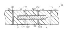
- a substrate 109 shown in FIG. 11 includes a capacitor 101 incorporated therein, and the capacitor 101 includes a first electrode 110, a dielectric layer 130 provided on the first electrode 110, and a dielectric layer 130.
- a first electrode 110 and a second electrode 120 facing each other are provided.
- a wiring 171 electrically connected to the first electrode 110 and a wiring 172 electrically connected to the second electrode 120 are formed on one surface of the substrate 109.
- the second electrode 120 constituting the upper electrode is connected to the wiring 172 through one via 162.
- the first electrode 110 constituting the lower electrode is connected to the wiring 173 provided on the surface opposite to the wiring 171 through the via 163, and the wiring 173 is connected to the wiring 171 through the via 161.
- the first electrode 110 is connected to the wiring 171.
- the capacitor 101 shown in FIG. 11 is built in the substrate 109, in order to connect the wiring 171 provided on one surface of the substrate 109 to the first electrode 110, the one surface of the substrate 109 is connected to the other surface.
- the via 161 reaching the first electrode 110 is formed, and the via 163 extending from the other surface to the first electrode 110 is formed.
- the conductive path from one surface of the substrate 109 to the first electrode 110 is long.
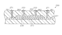
- FIG. 1 As a capacitor that can connect the wiring provided on one surface of the substrate to the first electrode and the second electrode without forming a via from one surface of the substrate to the other surface, for example, FIG. The following can be considered.
- a capacitor 201 built in the substrate 209 shown in FIG. 12 includes a first electrode 210 having a size larger than that of the dielectric layer 230 and the second electrode 220, and the second electrode 220 constituting the upper electrode has one via 262.
- the first electrode 210 constituting the lower electrode is also connected to the wiring 271 through one via 261.
- the first electrode 210 and the second electrode 220 It becomes difficult to properly form the vias 261 and 262 to be connected.
- the vias connected to the first electrode 210 and the second electrode 220 are not limited to the lengths of the vias 261 and 262, and the materials forming the first electrode 210 and the second electrode 220 are different from each other. It becomes difficult to form 261,262 appropriately.
- the vias connected to the first electrode and the second electrode constituting the substrate built-in capacitor cannot be properly formed, the vias formed on the substrate cannot be connected well to the first electrode and the second electrode. There is a problem.
- the present invention has been made in view of such circumstances, and an object thereof is to satisfactorily connect a via formed in a substrate to the first electrode and the second electrode, and to reduce the thickness.
- An object of the present invention is to provide a substrate built-in capacitor, a capacitor built-in substrate, and a method for manufacturing the substrate built-in capacitor.
- a substrate built-in capacitor according to the present invention includes a first electrode extending in a predetermined direction, a dielectric layer provided on the first electrode, and a dielectric layer provided on the dielectric layer.
- An electrode layer, and an end of the second electrode in the predetermined direction is connected to the electrode layer, and the surface of the electrode layer is disposed on the same plane as the surface of the first electrode. It is characterized by being.
- a substrate with a built-in capacitor is a substrate with a built-in capacitor in which a built-in capacitor is built-in, wherein the built-in capacitor has a first electrode extending in a predetermined direction, A dielectric layer provided on one electrode; and an end provided on the dielectric layer, facing the first electrode through the dielectric layer and projecting from the dielectric layer in the predetermined direction.
- a second electrode having an electrode layer spaced from the first electrode in the predetermined direction, an end of the second electrode and the electrode layer are connected, and the electrode layer and the first electrode One electrode is formed of the same material.
- a method of manufacturing a capacitor for incorporating a substrate according to the present invention includes a dielectric layer forming step of forming a dielectric layer on a first electrode layer, and the dielectric on the dielectric layer.
- the via formed in the substrate, the first electrode and the second electrode can be satisfactorily connected, the substrate built-in capacitor can be thinned, and the second from the one surface of the substrate.
- the conductive path leading to the electrode can be shortened.
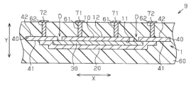
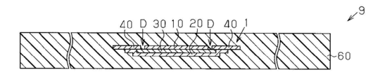
- FIG. 1 is a cross-sectional view showing a schematic configuration of a substrate built-in capacitor according to an embodiment of the present invention and a capacitor built-in substrate in which the capacitor is built.
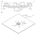
- the top view which shows the capacitor for a board
- Sectional drawing which shows schematic structure of the capacitor for a board
- Sectional drawing which shows schematic structure of the capacitor for a board
- a capacitor 1 according to the present invention is a substrate built-in capacitor built in a substrate 9.
- An arrow X in the figure indicates a surface direction X that is a predetermined linear direction.
- An arrow Y in the drawing indicates a thickness direction Y that is a direction perpendicular to the surface direction X.
- the capacitor 1 includes a first electrode 10, a dielectric layer 30 provided on the first electrode 10, and a second electrode provided on the dielectric layer 30 and facing the first electrode 10 through the dielectric layer 30. 20 and an electrode layer 40 which is connected to the second electrode 20 and located on the same plane as the first electrode 10.
- FIG. 2 which is a plan view of the capacitor 1, in the present embodiment, the first electrode 10, the second electrode 20, and the dielectric layer 30 have a rectangular shape.
- a portion indicated by a broken line H1 indicates a portion to which the via 61 shown in FIG. 1 is connected.
- a portion indicated by a broken line H2 indicates a portion to which the via 62 shown in FIG. 1 is connected.
- the first electrode 10 made of a conductive material such as metal is formed of a metal foil made of a metal such as copper, nickel, aluminum, or platinum, or a metal foil made of an alloy containing two or more of these metals. .
- the thin flat plate-like first electrode 10 has a surface 11 on which the dielectric layer 30 is provided and a surface 12 to which the via 61 is connected.
- the second electrode 20 made of a conductive material such as metal is formed of a metal film made of a metal such as copper, nickel, aluminum, or platinum, or a metal film made of an alloy containing two or more of these metals. .
- the thin film-like second electrode 20 is formed so as to sandwich the dielectric layer 30 together with the first electrode 10 in the thickness direction Y.
- the second electrode 20 has a larger dimension in the plane direction X than the first electrode 10 and the dielectric layer 30.
- the second electrode 20 extending in the plane direction X covers the lower part of the dielectric layer 30 as a lower electrode in FIG. Further, the second electrode 20 protrudes from both end portions of the dielectric layer 30 in the surface direction X and covers both end surfaces of the dielectric layer 30 in the surface direction X.
- both end portions of the second electrode 20 in the plane direction X are connected to the electrode layer 40. That is, the second electrode 20 has an end protruding from the dielectric layer 30 in the plane direction X, and the end of the second electrode 20 in the plane direction X is connected to the electrode layer 40.
- the dielectric layer 30 formed of a dielectric is formed of, for example, an oxide ceramic. Specifically, for example, metal oxides such as barium titanate, lithium niobate, lithium borate, lead zirconate titanate, strontium titanate, lead lanthanum zirconate titanate, lithium tantalate, zinc oxide, tantalum oxide, etc. Thus, the dielectric layer 30 is formed.
- the dielectric layer 30 may contain an additive for improving the dielectric characteristics in addition to the above metal oxide.
- the dielectric layer 30 provided on the surface 11 of the first electrode 10 has a size larger than that of the first electrode 10 in the surface direction X, and protrudes from both ends of the first electrode 10 in the surface direction X.
- the electrode layer 40 made of a conductive material such as a metal is formed of a metal foil such as a copper foil or a nickel foil, and is formed of the same material as the first electrode 10.
- the thin flat electrode layer 40 has a surface 41 to which the second electrode 20 is connected and a surface 42 to which the via 62 is connected.
- the electrode layer 40 extending in the plane direction X is formed so as to sandwich both end portions of the dielectric layer 30 together with the second electrode 20 in the thickness direction Y, and is provided at a distance from the first electrode 10 in the plane direction X. ing.
- a rectangular frame-shaped separation groove D is provided between the first electrode 10 and the electrode layer 40.
- Separation grooves D provided at portions other than the periphery of the dielectric layer 30 include end surfaces of the first electrode 10 and the electrode layer 40 in the surface direction X where the first electrode 10 and the electrode layer 40 face each other, and the dielectric layer. And a part of the surface of the dielectric layer 30 and having the surface of the dielectric layer 30 as a bottom surface.
- a part of the electrode layer 40 is provided at the end of the dielectric layer 30 in the plane direction X, and the part of the electrode layer 40 and the second electrode 20 face each other with the dielectric layer 30 in between.
- a separation groove D that electrically separates the first electrode 10 and the second electrode 20 is formed between the electrode layer 40 and the first electrode 10 with the portion excluding the periphery of the dielectric layer 30 as a bottom surface. ing.
- the first electrode 10 and the electrode layer 40 have the same thickness (dimension in the thickness direction Y). Therefore, the surface 11 of the first electrode 10 and the surface 41 of the electrode layer 40 are located on the same plane, and the surface 12 of the first electrode 10 and the surface 42 of the electrode layer 40 are located on the same plane. .
- the substrate 9 is a capacitor built-in substrate in which the capacitor 1 having the above-described configuration is built.
- the substrate 9 includes a capacitor 1 and an insulating substrate 60 in which the capacitor 1 is built.
- a via 61 electrically connected to the first electrode 10 is formed, and the second electrode 20 is formed.
- a via 62 electrically connected to is formed.
- the via 62 is electrically connected to the second electrode 20 by being connected to the electrode layer 40.
- a wiring 71 electrically connected to the first electrode 10 and a wiring 72 connected to the second electrode 20 are formed on the surface of the insulating substrate 60.
- the wirings 71 and 72 are provided on one surface of the substrate 9.
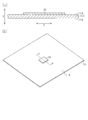
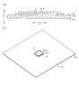
- FIGS. 3 (a), 4 (a), and 6 (a) are views along the alternate long and short dash line in FIGS. 3 (b), 4 (b), and 6 (b), respectively. It is sectional drawing.
- a first electrode layer 10A having a predetermined thickness that is easy to handle and hardly deforms in an annealing process described later is prepared.
- 10 A of 1st electrode layers are metal foil, Comprising: It is preferable that it is copper foil with high electroconductivity and easy acquisition.
- a dielectric layer 30 is formed on a part of the surface 11A of the first electrode layer 10A. That is, the dielectric layer 30 is formed on the first electrode layer 10A as a base (dielectric layer forming step).
- the dielectric layer 30 is formed by a powder spray coating method in which a powdery dielectric is sprayed.
- a powder spray coating method for example, an aerosol deposition method or a powder jet deposition method can be used.
- a powder jet deposition method In order to easily form the dielectric layer 30 in a room temperature and atmospheric pressure environment, it is preferable to use a powder jet deposition method.
- the dielectric layer 30 is annealed (annealing step).
- the annealing process is performed by, for example, laser irradiation to the dielectric layer 30, microwave heating, heating in an annealing furnace, or the like.
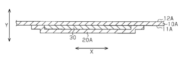
- a second electrode layer 20A that covers the dielectric layer 30 and is connected to the first electrode layer 10A is formed on the dielectric layer 30 (electrode).
- the second electrode layer 20A having a size larger than that of the dielectric layer 30 in the plane direction X is provided on the surface of the dielectric layer 30, and the end of the second electrode layer 20A in the plane direction X is a dielectric.
- the both end surfaces of the layer 30 are covered and provided on the surface of the first electrode layer 10 ⁇ / b> A around the dielectric layer 30.
- the second electrode layer 20A is preferably formed of the same material (that is, copper) as the first electrode layer 10A, but may be formed of a material different from that of the first electrode layer 10A.
- the second electrode layer 20A which is a metal film, is formed by, for example, sputtering, vapor deposition, conductive paste printing, plating, or a film forming method combining these.
- a film forming method in the electrode layer forming step it is preferable to adopt a method having high adhesion at the interface between the first electrode layer 10A and the dielectric layer 30 and the second electrode layer 20A.
- the first electrode layer 10A provided with the dielectric layer 30 and the second electrode layer 20A is inverted (inversion process).
- the first electrode layer 10A is thinned (thinning step). That is, the dimension of the first electrode layer 10A in the thickness direction Y is uniformly reduced in the plane direction X.
- the thinning process is an etching process in which the first electrode layer 10A is thinned by etching.
- Etching is chemical polishing using a chemical reaction that dissolves metal.
- dry etching using an etching gas or wet etching using an etching solution can be used as the etching in the etching step.
- the first electrode layer 10 ⁇ / b> A has a separation groove D that is a portion excluding the periphery of the dielectric layer 30 and has the surface of the dielectric layer 30 as a bottom surface.
- a separation groove D is formed in the first electrode layer 10A to electrically separate a portion facing the second electrode layer 20A via the dielectric layer 30 and a portion to which the second electrode layer 20A is connected. (Separation groove forming step).
- the first electrode 10 and the second electrode 20 which are not electrically connected are formed.
- the portion of the first electrode layer 10A that faces the second electrode layer 20A via the dielectric layer 30 becomes the first electrode 10, and the second electrode layer 20A.
- the portion of the first electrode layer 10 ⁇ / b> A to which both ends of the second electrode layer 20 ⁇ / b> A are connected becomes the electrode layer 40.
- the separation groove forming step is an electrode forming step in which the first electrode 10 and the second electrode 20 are formed by forming the separation groove D.
- the first electrode layer 10 ⁇ / b> A constitutes the first electrode 10 and the electrode layer 40
- the second electrode layer 20 ⁇ / b> A constitutes the second electrode 20.
- the surface 11A of the first electrode layer 10A constitutes the surfaces 11 and 41 of the first electrode 10 and the electrode layer 40
- the surface 12A of the first electrode layer 10A is the surface of the first electrode 10 and the electrode layer 40. 12 and 42 are configured.
- the method for manufacturing the capacitor 1 includes the dielectric layer forming step, the annealing step, the electrode layer forming step, the inversion step, the thinning step (etching step), and the separation groove forming step. Through these steps, the capacitor 1 is manufactured.
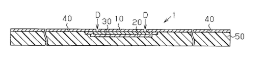
- the insulator 50 includes a core material and a pair of prepregs that sandwich the core material.
- the capacitor 1 is pressure-bonded to the semi-cured prepreg by heating and pressurizing the insulator 50.
- the insulator 50 may be prepared in advance, and the capacitor 1 may be laminated on the cured prepreg via an adhesive layer (not shown).
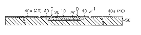
- the internal wiring 40a is formed by etching the electrode layer 40 (internal wiring forming step). That is, the electrode layer 40 included in the capacitor 1 constitutes an internal wiring 40 a provided in the substrate 9.
- the internal wiring 40 a may be a wiring that is not connected to the capacitor 1 or may be a wiring that is connected to the electrode layer 40.
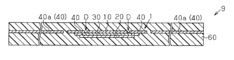
- another insulator 50 is stacked on the insulator 50 provided with the capacitor 1 by heating and pressing (insulator stacking layer step).
- insulator stacking layer step By performing the insulator stacking step, as shown in FIG. 9, an insulating substrate 60 is formed by the stacked insulators 50, and the substrate 9 in which the capacitor 1 is built is obtained.
- the method for manufacturing the substrate 9 includes the capacitor lamination process, the internal wiring formation process, the insulator lamination process, the via formation process, and the wiring formation process. Through these steps, the substrate 9 shown in FIG. 1 is manufactured.
- the capacitor 1 has a first electrode 10, a dielectric layer 30, and an end portion that projects from the dielectric layer 30 in the plane direction X while facing the first electrode 10 through the dielectric layer 30.
- a second electrode 20 and an electrode layer 40 provided at a distance from the first electrode 10 in the plane direction X are provided.
- the end of the second electrode 20 in the plane direction X is connected to the electrode layer 40, and the surface 42 that is the surface of the electrode layer 40 is positioned on the same plane as the surface 12 that is the surface of the first electrode 10. It is provided to do.
- the capacitor 1 having such a configuration is built in the substrate 9, in order to connect the wirings 71 and 72 provided on one surface of the substrate 9 to the first electrode 10 and the second electrode 20, Vias 61 and 62 extending from one surface of the electrode layer 40 to the surface of the electrode layer 40 and the surface of the first electrode 10 are formed in the substrate 9. Then, by connecting the via 62 to the electrode layer 40, the wiring 72 provided on one surface of the substrate 9 and the second electrode 20 are connected, and the via 61 is directly connected to the first electrode 10. Thus, the wiring 71 provided on one surface of the substrate 9 and the first electrode 10 are connected.
- the surface 42 of the electrode layer 40 connected to the second electrode 20 is provided so as to be located on the same plane as the surface 12 of the first electrode 10.
- the length of the via 61 electrically connected to the first electrode 10 and the length of the via 62 electrically connected to the second electrode 20 can be made the same.
- the capacitor 1 is built in the substrate 9, and the wirings 71 and 72 provided on one surface of the substrate 9 through the vias 61 and 62 formed in the substrate 9 are connected to the first electrode 10 and the second electrode 20.
- the vias 61 and 62 connected to the first electrode 10 and the second electrode 20 can be easily formed as compared with the case where the lengths of the vias 61 and 62 are different.
- the vias 61 and 62 formed in the substrate 9 and the first electrode 10 and the second electrode 20 can be satisfactorily connected. Further, when the capacitor 1 having the above configuration is built in the substrate 9, it is not necessary to form a via whose bottom surface is the surface of the second electrode 20, and the surface of the electrode layer 40 and the surface of the first electrode 10 are the bottom surface. The vias 61 and 62 may be formed. For this reason, it is not necessary to secure the thickness of the second electrode 20 in preparation for the formation of the vias 61 and 62, and the increase in the thickness of the second electrode 20 can be suppressed. Therefore, the capacitor 1 can be thinned.
- a part of the electrode layer 40 is provided at the end of the dielectric layer 30, and the part of the electrode layer 40 and the second electrode 20 face each other with the dielectric layer 30 interposed therebetween.
- a separation groove D for electrically separating the first electrode 10 and the second electrode 20 is provided between the first electrode 10 and the portion excluding the periphery of the dielectric layer 30 as a bottom surface. For this reason, since the edge part of the dielectric material layer 30 is pinched
- the vias 61 and 62 connected to 20 can be easily formed, and the vias 61 and 62 and the first electrode 10 and the second electrode 20 can be connected well. That is, even when the surface 42 of the electrode layer 40 and the surface 12 of the first electrode 10 are not completely located on the same plane, the vias 61 connected to the first electrode 10 and the second electrode 20, 62 can be formed easily.
- the thin substrate 9 can be used as a component built in an electronic device (not shown). As described in (4) above, in a state where the capacitor 1 is built in the substrate 9, the surface 42 of the electrode layer 40 is completely located on the same plane as the surface 12 of the first electrode 10. It does not have to be.
- the manufacturing method of the capacitor 1 includes a dielectric layer forming step of forming the dielectric layer 30, and an electrode layer formation of covering the dielectric layer 30 and forming the second electrode layer 20A connected to the first electrode layer 10A.
- the process includes a separation groove forming step of forming, in the first electrode layer 10A, a separation groove D that electrically separates a portion facing the second electrode layer 20A and a portion to which the second electrode layer 20A is connected.
- the separation groove D is formed in the first electrode layer 10A to which the second electrode layer 20A covering the dielectric layer 30 is connected, so that the first electrode layer 10A has the dielectric layer 30 interposed therebetween.
- the portion facing the second electrode layer 20 ⁇ / b> A becomes the first electrode 10
- the second electrode layer 20 ⁇ / b> A becomes the second electrode 20.
- the portion of the first electrode layer 10 ⁇ / b> A to which the second electrode layer 20 ⁇ / b> A is connected becomes the electrode layer 40 that is provided at a distance from the first electrode 10.
- the electrode layer 40 formed through the separation groove forming step is a part of the first electrode layer 10A before the separation groove forming step, and the electrode layer 40 is connected to the first electrode 10. It is provided similarly.
- the surface 42 of the electrode layer 40 connected to the first electrode 10 is provided so as to be located on the same plane as the surface 12 of the first electrode 10, and the electrode layer 40 and the first electrode 10 are the same. It is made of material. For this reason, the effect according to said (1), (2), and (4) can be acquired.
- the separation groove D is formed in a portion excluding the peripheral edge of the dielectric layer 30 and a part of the dielectric layer 30 is a bottom surface. Accordingly, a part of the electrode layer 40 is provided at the end of the dielectric layer 30, and the part of the electrode layer 40 and the second electrode 20 face each other with the dielectric layer 30 interposed therebetween. The end portion is sandwiched between a part of the electrode layer 40 and the second electrode 20. For this reason, the effect according to said (3) can be acquired.
- the method for manufacturing the capacitor 1 includes a thinning step for thinning the first electrode layer 10A after the dielectric layer forming step. This facilitates handling of the first electrode layer 10A until the dielectric layer 30 is formed, including when the dielectric layer 30 is formed. Further, since the first electrode layer 10A is thinned in the thinning step, the capacitor 1 can be thinned (so-called low profile).
- the method for manufacturing the capacitor 1 includes an annealing step of annealing the dielectric layer 30 after the dielectric layer forming step. For this reason, the ferroelectric characteristics of the dielectric layer 30 can be improved. If the thinning process is performed after the annealing process, the oxide film formed on the first electrode layer 10A due to the annealing process can be removed in the thinning process. As a result, it is possible to increase the maximum heating temperature in the annealing process that has been set low in order to suppress the formation of the oxide film. If the thinning process is performed after the annealing process, the thickness of the first electrode layer 10A can be ensured in the annealing process. As a result, it is possible to reduce the height of the capacitor 1 while suppressing the deformation of the first electrode layer 10A due to the annealing treatment.
- the dielectric layer 30 is formed by a powder spray coating method. For this reason, the dielectric layer 30 can be formed at room temperature by an aerosol deposition method, a powder jet deposition method, or the like. As a result, a metal having a low melting point can be used as the first electrode layer 10A serving as a base.
- the thinning process is an etching process in which the first electrode layer 10A is thinned by etching. For this reason, the first electrode layer 10A can be thinned to a desired thickness by chemical polishing.
- the method for manufacturing the substrate 9 includes an internal wiring forming step of forming the internal wiring 40 a by etching the electrode layer 40. Therefore, the electrode layer 40 included in the capacitor 1 can be used for the internal wiring 40 a provided in the substrate 9.
- the separation groove D may not be formed in the first electrode layer 10A. That is, the manufacturing process of the capacitor 1 may be included in the manufacturing process of the substrate 9. The manufacturing process of the capacitor 1 and the substrate 9 in this case will be described below.
- the first electrode layer 10A obtained through the dielectric layer forming step, the annealing step, the electrode layer forming step, the inversion step, and the thinning step is laminated on the surface of the insulator 50 composed of the core material and the prepreg (electrode) Layer lamination step).
- the second electrode layer 20A and the first electrode layer 10A are pressure-bonded to the semi-cured prepreg by heating and pressurizing the insulator 50.
- the electrode layer stacking step the insulator 50 provided with the exposed first electrode layer 10A in which the separation groove D is not formed is obtained.
- a separation groove D is formed in the first electrode layer 10A provided in the insulator 50 (separation groove forming step).
- a substrate 9 shown in FIG. 9 is obtained by performing an internal wiring formation step and an insulator lamination step. And the board
- a separation groove forming step that is an electrode forming step is performed. Since the capacitance of the capacitor 1 depends on the area of the portion where the first electrode 10 and the second electrode 20 face each other, the formation position of the separation groove D is related to the capacitance of the capacitor 1. Therefore, by performing the separation groove forming step after the electrode layer stacking step, the capacitor 1 having a desired capacitance can be obtained when the substrate 9 is manufactured.
- the electrode layer 40 included in the capacitor 1 may not be used for the internal wiring 40 a provided in the substrate 9. That is, for example, as shown in FIG. 10, an electrode layer 40 having a smaller dimension in the surface direction X than the electrode layer 40 in the above embodiment may be used.
- the capacitor 1 is laminated on the surface of the insulator 50 in the same manner as the capacitor lamination step, and the insulator lamination step, via formation step, and wiring formation step are performed without going through the internal wiring formation step. After that, as shown in FIG. 10, the substrate 9 without the internal wiring 40a is manufactured.
- a plurality of dielectric layers 30 may be formed on one first electrode layer 10A.
- the first electrode layer 10A is cut in accordance with the shape of the dielectric layer 30, thereby manufacturing the plurality of capacitors 1 from one first electrode layer 10A. Also good.
- the second electrode 20 may be formed of a metal foil made of a metal such as copper, nickel, aluminum, or platinum, or a metal foil made of an alloy containing two or more of these metals. That is, the second electrode layer 20A may be composed of a metal foil. In this case, the second electrode is formed by attaching the metal foil to the first electrode layer 10A and the dielectric layer 30 in the electrode layer forming step. Layer 20A is formed.
- the metal foil constituting the first electrode layer 10A may be plated. Moreover, when the 2nd electrode layer 20A is comprised with metal foil as mentioned above, plating may be given to this metal foil.
- the dielectric layer 30 may be formed by a method other than the powder spray coating method.
- the dielectric layer 30 may be formed by sputtering, vapor deposition, sol-gel method, or the like.
- the annealing step may be omitted.
- the first electrode layer 10A may be thinned by a method other than etching. That is, the method for thinning the first electrode layer 10A is not limited to chemical polishing.
- the first electrode layer 10A may be thinned by mechanical polishing or chemical mechanical polishing.
- D Separation groove
- X Surface direction
- Y Thickness direction
- 1 Substrate built-in capacitor
- 9 Capacitor built-in substrate
- 10 First electrode, 11, 12 ... Surface
- 10A First electrode layer
- 11A, 12A ... surface
- 20 ... second electrode 20A ... second electrode layer
- 30 ... dielectric layer
- 40 ... electrode layer, 40a internal wiring, 41, 42 ... surface, 50 ... insulator, 60 ... insulating substrate, 61, 62 ... via, 71, 72 ... wiring.
Landscapes
- Engineering & Computer Science (AREA)
- Power Engineering (AREA)
- Microelectronics & Electronic Packaging (AREA)
- Manufacturing & Machinery (AREA)
- Chemical & Material Sciences (AREA)
- Ceramic Engineering (AREA)
- Inorganic Chemistry (AREA)
- Fixed Capacitors And Capacitor Manufacturing Machines (AREA)
- Ceramic Capacitors (AREA)
- Production Of Multi-Layered Print Wiring Board (AREA)
Abstract
Priority Applications (3)
| Application Number | Priority Date | Filing Date | Title |
|---|---|---|---|
| US13/812,348 US20130120902A1 (en) | 2010-07-30 | 2011-07-07 | Substrate-incorporated capacitor, capacitor-incorporating substrate provided with the same, and method for manufacturing substrate-incorporated capacitor |
| JP2012526399A JPWO2012014648A1 (ja) | 2010-07-30 | 2011-07-07 | 基板内蔵用キャパシタ、これを備えたキャパシタ内蔵基板、及び基板内蔵用キャパシタの製造方法 |
| CN201180037590XA CN103053002A (zh) | 2010-07-30 | 2011-07-07 | 基板内置用电容器、具备其的电容器内置基板及基板内置用电容器的制造方法 |
Applications Claiming Priority (2)
| Application Number | Priority Date | Filing Date | Title |
|---|---|---|---|
| JP2010173037 | 2010-07-30 | ||
| JP2010-173037 | 2010-07-30 |
Publications (1)
| Publication Number | Publication Date |
|---|---|
| WO2012014648A1 true WO2012014648A1 (fr) | 2012-02-02 |
Family
ID=45529866
Family Applications (1)
| Application Number | Title | Priority Date | Filing Date |
|---|---|---|---|
| PCT/JP2011/065545 Ceased WO2012014648A1 (fr) | 2010-07-30 | 2011-07-07 | Condensateur pour incorporation dans un substrat, substrat à condensateur incorporé mettant en oeuvre ce condensateur, et procédé de fabrication de ce condensateur |
Country Status (4)
| Country | Link |
|---|---|
| US (1) | US20130120902A1 (fr) |
| JP (1) | JPWO2012014648A1 (fr) |
| CN (1) | CN103053002A (fr) |
| WO (1) | WO2012014648A1 (fr) |
Cited By (2)
| Publication number | Priority date | Publication date | Assignee | Title |
|---|---|---|---|---|
| JP2018137311A (ja) * | 2017-02-21 | 2018-08-30 | Tdk株式会社 | 薄膜キャパシタ |
| US10178717B2 (en) | 2017-03-09 | 2019-01-08 | Dongming Li | Lamp-control circuit for lamp array emitting constant light output |
Families Citing this family (3)
| Publication number | Priority date | Publication date | Assignee | Title |
|---|---|---|---|---|
| KR20160000753A (ko) * | 2014-06-25 | 2016-01-05 | 삼성전기주식회사 | 박막형 커패시터 소자 및 이의 제조 방법 |
| US10468187B2 (en) * | 2016-08-05 | 2019-11-05 | Samsung Electro-Mechanics Co., Ltd. | Thin-film ceramic capacitor having capacitance forming portions separated by separation slit |
| KR101912282B1 (ko) | 2016-08-05 | 2018-10-29 | 삼성전기 주식회사 | 박막 커패시터 |
Citations (4)
| Publication number | Priority date | Publication date | Assignee | Title |
|---|---|---|---|---|
| JPH1126943A (ja) * | 1997-06-30 | 1999-01-29 | Kyocera Corp | 多層配線基板およびその製造方法 |
| JP2000049041A (ja) * | 1998-07-31 | 2000-02-18 | Sony Corp | コンデンサ |
| JP2007035975A (ja) * | 2005-07-27 | 2007-02-08 | Mitsui Mining & Smelting Co Ltd | 支持基板付キャパシタ層形成材及びキャパシタ層形成材並びにこれらの製造方法 |
| JP2010157529A (ja) * | 2008-12-26 | 2010-07-15 | Tdk Corp | 誘電体薄膜素子の製造方法 |
Family Cites Families (13)
| Publication number | Priority date | Publication date | Assignee | Title |
|---|---|---|---|---|
| JPH0286111A (ja) * | 1988-09-22 | 1990-03-27 | Nippon Oil & Fats Co Ltd | 単一面に端子引き出し可能なコンデンサ |
| US5708559A (en) * | 1995-10-27 | 1998-01-13 | International Business Machines Corporation | Precision analog metal-metal capacitor |
| JPH1092689A (ja) * | 1996-09-13 | 1998-04-10 | Toshiba Corp | キャパシタおよびその製造方法 |
| US6404615B1 (en) * | 2000-02-16 | 2002-06-11 | Intarsia Corporation | Thin film capacitors |
| JP4239526B2 (ja) * | 2002-08-30 | 2009-03-18 | Toto株式会社 | コンデンサ、複合回路基板及びコンデンサの製造方法 |
| US20050063135A1 (en) * | 2003-09-18 | 2005-03-24 | Borland William J. | High tolerance embedded capacitors |
| US20040099999A1 (en) * | 2002-10-11 | 2004-05-27 | Borland William J. | Co-fired capacitor and method for forming ceramic capacitors for use in printed wiring boards |
| US7705423B2 (en) * | 2005-10-21 | 2010-04-27 | Georgia Tech Research Corporation | Device having an array of embedded capacitors for power delivery and decoupling of high speed input/output circuitry of an integrated circuit |
| US7456459B2 (en) * | 2005-10-21 | 2008-11-25 | Georgia Tech Research Corporation | Design of low inductance embedded capacitor layer connections |
| US20070236859A1 (en) * | 2006-04-10 | 2007-10-11 | Borland William J | Organic encapsulant compositions for protection of electronic components |
| US20080308309A1 (en) * | 2007-06-14 | 2008-12-18 | Phoenix Precision Technology Corporation | Structure of packaging substrate having capacitor embedded therein and method for fabricating the same |
| US8391017B2 (en) * | 2009-04-28 | 2013-03-05 | Georgia Tech Research Corporation | Thin-film capacitor structures embedded in semiconductor packages and methods of making |
| US8088658B2 (en) * | 2009-04-28 | 2012-01-03 | E. I. Du Pont De Nemours And Company | Thin film capacitor and method of fabrication thereof |
-
2011
- 2011-07-07 WO PCT/JP2011/065545 patent/WO2012014648A1/fr not_active Ceased
- 2011-07-07 JP JP2012526399A patent/JPWO2012014648A1/ja not_active Withdrawn
- 2011-07-07 CN CN201180037590XA patent/CN103053002A/zh active Pending
- 2011-07-07 US US13/812,348 patent/US20130120902A1/en not_active Abandoned
Patent Citations (4)
| Publication number | Priority date | Publication date | Assignee | Title |
|---|---|---|---|---|
| JPH1126943A (ja) * | 1997-06-30 | 1999-01-29 | Kyocera Corp | 多層配線基板およびその製造方法 |
| JP2000049041A (ja) * | 1998-07-31 | 2000-02-18 | Sony Corp | コンデンサ |
| JP2007035975A (ja) * | 2005-07-27 | 2007-02-08 | Mitsui Mining & Smelting Co Ltd | 支持基板付キャパシタ層形成材及びキャパシタ層形成材並びにこれらの製造方法 |
| JP2010157529A (ja) * | 2008-12-26 | 2010-07-15 | Tdk Corp | 誘電体薄膜素子の製造方法 |
Cited By (2)
| Publication number | Priority date | Publication date | Assignee | Title |
|---|---|---|---|---|
| JP2018137311A (ja) * | 2017-02-21 | 2018-08-30 | Tdk株式会社 | 薄膜キャパシタ |
| US10178717B2 (en) | 2017-03-09 | 2019-01-08 | Dongming Li | Lamp-control circuit for lamp array emitting constant light output |
Also Published As
| Publication number | Publication date |
|---|---|
| JPWO2012014648A1 (ja) | 2013-09-12 |
| CN103053002A (zh) | 2013-04-17 |
| US20130120902A1 (en) | 2013-05-16 |
Similar Documents
| Publication | Publication Date | Title |
|---|---|---|
| US10079108B2 (en) | Multilayer capacitor and mounting structure | |
| US11375620B2 (en) | Multi-layer ceramic electronic component, method of producing a multi-layer ceramic electronic component, and substrate with a built-in electronic component | |
| JP5206440B2 (ja) | セラミック電子部品 | |
| JP2018018938A (ja) | 積層セラミック電子部品 | |
| US11145464B2 (en) | Multilayer ceramic capacitor and method of manufacturing the same | |
| CN108231336B (zh) | 电感器 | |
| KR101886332B1 (ko) | 전자부품 및 전자부품 내장형 기판 | |
| CN104347270A (zh) | 多层陶瓷电子部件、其上安装有该部件的板及其制造方法 | |
| CN104051155A (zh) | 嵌入式多层陶瓷电子元件和具有该电子元件的印刷电路板 | |
| CN103903855A (zh) | 多层陶瓷电容器及其制造方法 | |
| JP2001196228A (ja) | 積層セラミック電子部品の製造方法及び積層セラミック電子部品 | |
| JP2017108057A (ja) | 積層セラミックコンデンサ | |
| US20170287642A1 (en) | Multi-layer ceramic electronic component and method of producing the same | |
| JP2014187216A (ja) | 積層セラミックコンデンサの製造方法 | |
| JP2015076600A (ja) | 基板内蔵用積層セラミック電子部品及び積層セラミック電子部品内蔵型印刷回路基板 | |
| JP2012009679A (ja) | セラミック電子部品及びその製造方法 | |
| WO2012014648A1 (fr) | Condensateur pour incorporation dans un substrat, substrat à condensateur incorporé mettant en oeuvre ce condensateur, et procédé de fabrication de ce condensateur | |
| JP2022032641A (ja) | 部品内蔵基板 | |
| US20230207220A1 (en) | Multilayer electronic component | |
| JP2012227240A (ja) | 積層構造体及びその製造方法 | |
| WO2012014647A1 (fr) | Condensateur pour incorporation dans un substrat, substrat à condensateur incorporé mettant en oeuvre ce condensateur, et procédé de fabrication de ce condensateur | |
| WO2012014646A1 (fr) | Procédé de fabrication de condensateur pour incorporation dans un substrat, et substrat à condensateur incorporé associé | |
| JP2004289085A (ja) | 薄膜積層電子部品及びその製造方法 | |
| JP2015088616A (ja) | セラミック電子部品 | |
| JP2002110451A (ja) | 積層型電子部品およびその製法 |
Legal Events
| Date | Code | Title | Description |
|---|---|---|---|
| WWE | Wipo information: entry into national phase |
Ref document number: 201180037590.X Country of ref document: CN |
|
| 121 | Ep: the epo has been informed by wipo that ep was designated in this application |
Ref document number: 11812240 Country of ref document: EP Kind code of ref document: A1 |
|
| WWE | Wipo information: entry into national phase |
Ref document number: 2012526399 Country of ref document: JP |
|
| WWE | Wipo information: entry into national phase |
Ref document number: 13812348 Country of ref document: US |
|
| NENP | Non-entry into the national phase |
Ref country code: DE |
|
| 122 | Ep: pct application non-entry in european phase |
Ref document number: 11812240 Country of ref document: EP Kind code of ref document: A1 |