WO2012014992A1 - 不揮発性半導体メモリ装置及びその製造方法、並びに電荷蓄積膜 - Google Patents
不揮発性半導体メモリ装置及びその製造方法、並びに電荷蓄積膜 Download PDFInfo
- Publication number
- WO2012014992A1 WO2012014992A1 PCT/JP2011/067309 JP2011067309W WO2012014992A1 WO 2012014992 A1 WO2012014992 A1 WO 2012014992A1 JP 2011067309 W JP2011067309 W JP 2011067309W WO 2012014992 A1 WO2012014992 A1 WO 2012014992A1
- Authority
- WO
- WIPO (PCT)
- Prior art keywords
- film
- memory device
- semiconductor memory
- silicon nitride
- chemical vapor
- Prior art date
- Legal status (The legal status is an assumption and is not a legal conclusion. Google has not performed a legal analysis and makes no representation as to the accuracy of the status listed.)
- Ceased
Links
Images





Classifications
-
- C—CHEMISTRY; METALLURGY
- C23—COATING METALLIC MATERIAL; COATING MATERIAL WITH METALLIC MATERIAL; CHEMICAL SURFACE TREATMENT; DIFFUSION TREATMENT OF METALLIC MATERIAL; COATING BY VACUUM EVAPORATION, BY SPUTTERING, BY ION IMPLANTATION OR BY CHEMICAL VAPOUR DEPOSITION, IN GENERAL; INHIBITING CORROSION OF METALLIC MATERIAL OR INCRUSTATION IN GENERAL
- C23C—COATING METALLIC MATERIAL; COATING MATERIAL WITH METALLIC MATERIAL; SURFACE TREATMENT OF METALLIC MATERIAL BY DIFFUSION INTO THE SURFACE, BY CHEMICAL CONVERSION OR SUBSTITUTION; COATING BY VACUUM EVAPORATION, BY SPUTTERING, BY ION IMPLANTATION OR BY CHEMICAL VAPOUR DEPOSITION, IN GENERAL
- C23C16/00—Chemical coating by decomposition of gaseous compounds, without leaving reaction products of surface material in the coating, i.e. chemical vapour deposition [CVD] processes
- C23C16/22—Chemical coating by decomposition of gaseous compounds, without leaving reaction products of surface material in the coating, i.e. chemical vapour deposition [CVD] processes characterised by the deposition of inorganic material, other than metallic material
- C23C16/30—Deposition of compounds, mixtures or solid solutions, e.g. borides, carbides, nitrides
- C23C16/34—Nitrides
- C23C16/345—Silicon nitride
-
- H—ELECTRICITY
- H10—SEMICONDUCTOR DEVICES; ELECTRIC SOLID-STATE DEVICES NOT OTHERWISE PROVIDED FOR
- H10B—ELECTRONIC MEMORY DEVICES
- H10B43/00—EEPROM devices comprising charge-trapping gate insulators
- H10B43/30—EEPROM devices comprising charge-trapping gate insulators characterised by the memory core region
-
- H—ELECTRICITY
- H10—SEMICONDUCTOR DEVICES; ELECTRIC SOLID-STATE DEVICES NOT OTHERWISE PROVIDED FOR
- H10D—INORGANIC ELECTRIC SEMICONDUCTOR DEVICES
- H10D30/00—Field-effect transistors [FET]
- H10D30/60—Insulated-gate field-effect transistors [IGFET]
- H10D30/69—IGFETs having charge trapping gate insulators, e.g. MNOS transistors
-
- H—ELECTRICITY
- H10—SEMICONDUCTOR DEVICES; ELECTRIC SOLID-STATE DEVICES NOT OTHERWISE PROVIDED FOR
- H10D—INORGANIC ELECTRIC SEMICONDUCTOR DEVICES
- H10D64/00—Electrodes of devices having potential barriers
- H10D64/01—Manufacture or treatment
- H10D64/031—Manufacture or treatment of data-storage electrodes
- H10D64/037—Manufacture or treatment of data-storage electrodes comprising charge-trapping insulators
-
- H—ELECTRICITY
- H10—SEMICONDUCTOR DEVICES; ELECTRIC SOLID-STATE DEVICES NOT OTHERWISE PROVIDED FOR
- H10P—GENERIC PROCESSES OR APPARATUS FOR THE MANUFACTURE OR TREATMENT OF DEVICES COVERED BY CLASS H10
- H10P14/00—Formation of materials, e.g. in the shape of layers or pillars
- H10P14/60—Formation of materials, e.g. in the shape of layers or pillars of insulating materials
- H10P14/63—Formation of materials, e.g. in the shape of layers or pillars of insulating materials characterised by the formation processes
- H10P14/6302—Non-deposition formation processes
- H10P14/6316—Formation by nitridation, e.g. nitridation of the substrate
-
- H—ELECTRICITY
- H10—SEMICONDUCTOR DEVICES; ELECTRIC SOLID-STATE DEVICES NOT OTHERWISE PROVIDED FOR
- H10P—GENERIC PROCESSES OR APPARATUS FOR THE MANUFACTURE OR TREATMENT OF DEVICES COVERED BY CLASS H10
- H10P14/00—Formation of materials, e.g. in the shape of layers or pillars
- H10P14/60—Formation of materials, e.g. in the shape of layers or pillars of insulating materials
- H10P14/63—Formation of materials, e.g. in the shape of layers or pillars of insulating materials characterised by the formation processes
- H10P14/6326—Deposition processes
- H10P14/6328—Deposition from the gas or vapour phase
- H10P14/6334—Deposition from the gas or vapour phase using decomposition or reaction of gaseous or vapour phase compounds, i.e. chemical vapour deposition
-
- H—ELECTRICITY
- H10—SEMICONDUCTOR DEVICES; ELECTRIC SOLID-STATE DEVICES NOT OTHERWISE PROVIDED FOR
- H10P—GENERIC PROCESSES OR APPARATUS FOR THE MANUFACTURE OR TREATMENT OF DEVICES COVERED BY CLASS H10
- H10P14/00—Formation of materials, e.g. in the shape of layers or pillars
- H10P14/60—Formation of materials, e.g. in the shape of layers or pillars of insulating materials
- H10P14/63—Formation of materials, e.g. in the shape of layers or pillars of insulating materials characterised by the formation processes
- H10P14/6326—Deposition processes
- H10P14/6328—Deposition from the gas or vapour phase
- H10P14/6334—Deposition from the gas or vapour phase using decomposition or reaction of gaseous or vapour phase compounds, i.e. chemical vapour deposition
- H10P14/6338—Deposition from the gas or vapour phase using decomposition or reaction of gaseous or vapour phase compounds, i.e. chemical vapour deposition the reactions being activated by other means than plasma or thermal, e.g. photo-CVD
-
- H—ELECTRICITY
- H10—SEMICONDUCTOR DEVICES; ELECTRIC SOLID-STATE DEVICES NOT OTHERWISE PROVIDED FOR
- H10P—GENERIC PROCESSES OR APPARATUS FOR THE MANUFACTURE OR TREATMENT OF DEVICES COVERED BY CLASS H10
- H10P14/00—Formation of materials, e.g. in the shape of layers or pillars
- H10P14/60—Formation of materials, e.g. in the shape of layers or pillars of insulating materials
- H10P14/66—Formation of materials, e.g. in the shape of layers or pillars of insulating materials characterised by the type of materials
- H10P14/668—Formation of materials, e.g. in the shape of layers or pillars of insulating materials characterised by the type of materials the materials being characterised by the deposition precursor materials
- H10P14/6681—Formation of materials, e.g. in the shape of layers or pillars of insulating materials characterised by the type of materials the materials being characterised by the deposition precursor materials the precursor containing a compound comprising Si
- H10P14/6682—Formation of materials, e.g. in the shape of layers or pillars of insulating materials characterised by the type of materials the materials being characterised by the deposition precursor materials the precursor containing a compound comprising Si the compound being a silane, e.g. disilane, methylsilane or chlorosilane
-
- H—ELECTRICITY
- H10—SEMICONDUCTOR DEVICES; ELECTRIC SOLID-STATE DEVICES NOT OTHERWISE PROVIDED FOR
- H10P—GENERIC PROCESSES OR APPARATUS FOR THE MANUFACTURE OR TREATMENT OF DEVICES COVERED BY CLASS H10
- H10P14/00—Formation of materials, e.g. in the shape of layers or pillars
- H10P14/60—Formation of materials, e.g. in the shape of layers or pillars of insulating materials
- H10P14/69—Inorganic materials
- H10P14/694—Inorganic materials composed of nitrides
- H10P14/6943—Inorganic materials composed of nitrides containing silicon
- H10P14/69433—Inorganic materials composed of nitrides containing silicon the material being a silicon nitride not containing oxygen, e.g. SixNy or SixByNz
Definitions
- the present invention relates to a nonvolatile semiconductor memory device, a manufacturing method thereof, and a charge storage film, and more particularly to a nonvolatile semiconductor memory device having a MONOS structure or a SONOS structure, a manufacturing method thereof, and a charge storage film of the memory device.
- a nonvolatile semiconductor memory device such as a flash memory has been developed and widely used as a storage medium.
- a MONOS (Metal-Oxide-Nitride-Oxide-Silicon) structure (MONOS-type memory cell structure) or a SONOS (Silicon-Silicon-silicon structure) using a silicon nitride film manufactured by LPCVD is used.
- a memory technology having an Oxide-Nitride-Oxide-Silicon structure (SONOS type memory cell structure) is known (for example, see Patent Document 1).
- the memory having such a structure does not lose its memory even after the power is turned off, and can perform high-speed writing and reading.
- the current main force is a floating gate type, and this floating gate functions as a region for accumulating and holding charges.
- a floating gate for example, a polycrystalline silicon film
- a tunnel insulating film also referred to as a gate insulating film
- a control gate electrode is formed on the semiconductor substrate on both sides of the control gate electrode, with a blocking insulating film (for example, a silicon oxide film or an aluminum oxide film) interposed therebetween. Source / drain regions are formed in the substrate.
- the blocking insulating film has a function of blocking current between the floating gate which is a charge storage film and the control electrode.
- a silicon nitride film is formed by LPCVD on a tunnel insulating film (for example, a silicon oxide film) provided on a semiconductor substrate.
- a nonvolatile semiconductor memory device in which a control gate electrode is formed with a blocking insulating film (for example, a silicon oxide film) interposed therebetween, and a source / drain region is formed on a semiconductor substrate on both sides of the control gate electrode. It has been.
- the source electrode when writing to the memory, the source electrode is usually grounded, a sufficiently high voltage is applied to the gate electrode and the drain electrode, and electrons are directed from the source electrode to the drain electrode.
- the electrons flowing through the channel portion become thermal electrons having a large momentum, and some of them pass through the tunnel insulating film and accumulate in the floating gate.
- the gate is closed after sufficient electrons are accumulated in the floating gate, the electrons accumulated in the floating gate can be blocked and held by the tunnel insulating film. That is, the information is stored.
- erasing information if the gate electrode is grounded and the source electrode is kept at a high potential, electrons are gradually removed from the floating gate and information storage is erased.
- a charge storage film in the nonvolatile semiconductor memory device having the above-described structure a charge storage film including at least a Si 3 N 4 film and an insulating film containing La and Si provided thereon has been proposed (for example, Patent Documents). 2).
- This silicon nitride film is manufactured by a normal CVD method, and the charge trap amount is increased by using a charge storage film having such a laminated structure.
- a silicon nitride film can be produced from SiH 4 gas and NH 3 gas by catalytic chemical vapor deposition (Cat-CVD method) (see, for example, Patent Document 3).
- the limit of miniaturization is pointed out due to the limit of the charge storage capability of the Si 3 N 4 film. Therefore, improvement of charge accumulation / holding characteristics (charge holding characteristics) of the Si 3 N 4 film is required.
- the limit of the principle miniaturization of each constituent film is pointed out, and the charge storage capability of the charge storage film is required to be improved.
- An object of the present invention is to solve the above-mentioned problems of the prior art, and has a charge storage film made of a silicon nitride film having high charge storage / holding characteristics, and can be miniaturized, for example, a MONOS structure
- Another object of the present invention is to provide a nonvolatile semiconductor memory device having a SONOS structure, a manufacturing method thereof, and the charge storage film.
- the nonvolatile semiconductor memory device of the present invention includes a tunnel insulating film on a semiconductor substrate, a charge storage film on the tunnel insulating film, a blocking insulating film on the charge storage film, and a control gate electrode on the blocking insulating film And a source / drain region formed in the semiconductor substrate on both sides of the control gate electrode, and the charge storage film is a silicon nitride film produced by catalytic chemical vapor deposition, The ratio N / Si is 1.2 to 1.4.
- the charge storage amount is increased and the charge retention characteristics are improved. Is achieved.
- the charge storage / retention characteristics tend to deteriorate, and if it exceeds 1.4, the insulation characteristics tend to deteriorate.
- the content of hydrogen atoms introduced into the silicon nitride film by catalytic chemical vapor deposition is 5 to 20 at%.
- the charge storage / retention characteristics tend to deteriorate, and when it exceeds 20 at%, the insulation characteristics tend to deteriorate.
- N—H bonds introduced into the silicon nitride film by catalytic chemical vapor deposition are 5 ⁇ 10 21 to 5 ⁇ 10 22 bonds / cm 3 .
- the N—H bond is less than 5 ⁇ 10 21 , the charge storage / retention characteristics tend to deteriorate, and if it exceeds 5 ⁇ 10 22 bonds / cm 3 , the insulation characteristics tend to deteriorate. .
- the nonvolatile semiconductor memory device of the present invention includes a tunnel insulating film on a semiconductor substrate, a charge storage film on the tunnel insulating film, a blocking insulating film on the charge storage film, and a control gate electrode on the blocking insulating film And a source / drain region formed in the semiconductor substrate on both sides of the control gate electrode, and the charge storage film is a silicon nitride film produced by catalytic chemical vapor deposition,
- the ratio N / Si is 1.2 to 1.4
- the content of hydrogen atoms introduced into the silicon nitride film by catalytic chemical vapor deposition is 5 to 20 at%
- the N—H bond introduced into the film by catalytic chemical vapor deposition is 5 ⁇ 10 21 to 5 ⁇ 10 22 / cm 3 .
- the silicon nitride film is decomposed by introducing SiH 4 and NH 3 gas into a vacuum chamber, contacting with a heated catalyst, and forming a film on a target heating surface disposed in the vacuum chamber. It is produced by a phase growth method.
- the silicon nitride film introduces SiH 4 , NH 3 , and H 2 gas into a vacuum chamber, is brought into contact with a heated catalyst, is decomposed, and is formed on a target heating surface disposed in the vacuum chamber. It is produced by catalytic chemical vapor deposition.
- the silicon nitride film is produced by catalytic chemical vapor deposition at a pressure of less than 100 Pa in a vacuum chamber.
- the lower limit is the pressure that can usually be achieved.
- the temperature of the target heating surface is 100 to 500 ° C.
- the desired silicon nitride film tends to be difficult to obtain.
- the catalyst is made of a material selected from at least one metal selected from W, Mo, and Ta, and an alloy including at least two of these metals.
- the heating temperature of the catalyst is 1500 to 2000 ° C.
- the heating temperature is out of the range, a desired silicon nitride film tends to be difficult to obtain.
- a method for manufacturing a nonvolatile semiconductor memory device includes a silicon nitride film formed by catalytic chemical vapor deposition on a tunnel insulating film formed on a semiconductor substrate, and formed on the tunnel insulating film, A charge storage film having an element ratio N / Si of 1.2 to 1.4 is formed, a blocking insulating film is formed on the charge storage film, a control gate electrode is formed on the blocking insulating film, and the control Source / drain regions are formed in the semiconductor substrate on both sides of the gate electrode.
- the content of hydrogen atoms introduced into the silicon nitride film by catalytic chemical vapor deposition is 5 to 20 at%.
- the number of NH bonds introduced into the silicon nitride film by catalytic chemical vapor deposition is 5 ⁇ 10 21 to 5 ⁇ 10 22 / cm 3.
- the silicon nitride film is decomposed by introducing SiH 4 and NH 3 gas into a vacuum chamber, contacting with a heated catalyst, and disposed in the vacuum chamber It is produced by a catalytic chemical vapor deposition method in which a film is formed on a heated surface.
- the silicon nitride film is decomposed by introducing SiH 4 , NH 3 , and H 2 gas into a vacuum chamber and contacting with a heated catalyst, It is produced by a catalytic chemical vapor deposition method in which a film is formed on a target heating surface that is arranged.
- the silicon nitride film is formed by catalytic chemical vapor deposition at a pressure of less than 100 Pa in a vacuum chamber.
- the temperature of the target heating surface is 100 to 500 ° C.
- the catalyst is made of a material selected from at least one metal selected from W, Mo, and Ta and an alloy including at least two of these metals. To do.
- the heating temperature of the catalyst is 1500 to 2000 ° C.
- the charge storage film of the present invention is a silicon nitride film produced by a catalytic chemical vapor deposition method and has a constituent element ratio N / Si of 1.2 to 1.4.
- the silicon nitride film contains 5 to 20 at% of hydrogen atoms introduced by catalytic chemical vapor deposition.
- the charge storage film is characterized in that the silicon nitride film has 5 ⁇ 10 21 to 5 ⁇ 10 22 bonds / cm 3 of NH bonds introduced by catalytic chemical vapor deposition.
- the use of a charge storage film made of a silicon nitride film manufactured by catalytic chemical vapor deposition with high charge retention characteristics avoids the limit of miniaturization and advances the integration.
- the nonvolatile semiconductor memory device for example, a memory device having a MONOS structure or a SONOS structure
- a memory device having a MONOS structure or a SONOS structure can be provided.
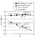
- 6 is a graph showing the relationship between the N / Si ratio and the midgap voltage (V) in order to study the influence of the N / Si ratio on the memory window (V) in the silicon nitride film obtained in Example 1.
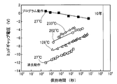
- 6 is a graph showing the relationship between retention time (seconds) and midgap voltage (V) in order to study the charge retention characteristics of a silicon nitride film produced by catalytic chemical vapor deposition in Example 2.
- the graph which shows the relationship between retention time (second) and mid gap voltage (V), in order to examine the charge retention characteristic of the silicon nitride film produced by the conventional LPCVD method.
- the graph which shows the Arrhenius plot which put together the result in Example 2.
- FIG. Shown by comparing the results of the charge retention characteristics of Example 2 obtained in catalytic chemical vapor deposition of silicon nitride film, LPCVD method using the Si 3 N 4 film and Si 3 N 4 film obtained by PECVD table.
- the nonvolatile semiconductor memory device includes a tunnel insulating film on a semiconductor substrate, a charge storage film on the tunnel insulating film, and the charge storage film.
- the silicon nitride film produced by the method has a constituent element ratio N / Si of 1.2 to 1.4 as measured by the method described below, and is introduced into the silicon nitride film by catalytic chemical vapor deposition
- the hydrogen atom content measured is 5 to 20 at% as measured by the method described below, and the NH bond introduced into the silicon nitride film by catalytic chemical vapor deposition is measured by the method described below.
- Consists is 5 ⁇ 10 21 ⁇ 5 ⁇ 10 22 / cm 3 or Te.
- the constituent element ratio N / Si is measured by Rutherford Backscattering Spectroscopy.
- the sample was irradiated with He + ions with an energy of 480 keV at an angle of 45 degrees with respect to the normal of the sample surface, and the scattered He + ions were detected with a deflection magnetic field energy analyzer at a scattering angle of 90 degrees. .
- the hydrogen atom content is measured by elastic recoil detection analysis.
- a method is used in which N + ions with an energy of 480 keV are irradiated to the sample at an angle of 70 degrees with respect to the normal of the sample surface, and the recoiled H + ions are detected with a deflection magnetic field type energy analyzer at a scattering angle of 30 degrees. It was.
- N—H bonds are measured by Fourier Transform Infrared Spectroscopy. The specific number of bonds is W.W. A. Lanford, M.C. J. et al. Calculation was performed using the conversion factor of Rand's paper (J. Appl. Phys. 49 (1978) 2473).
- the nonvolatile semiconductor memory device of the present invention has, for example, the MONOS type structure shown in FIG. 1, the tunnel insulating film 12 made of silicon oxide (SiO 2 ) formed on the Si substrate 11, and the tunnel insulating film Formed on the charge storage film 13 made of silicon nitride, a blocking insulating film 14 made of silicon oxide (SiO 2 ) formed on the charge storage film 13, and formed on the blocking insulating film 14.
- the control gate electrode 15 made of polysilicon or metal and the source region 16 / drain region 17 formed on the Si substrate 11 on both sides of the control gate electrode 15 are provided. A voltage is applied to the control gate electrode 15 It is configured to be able to.
- the blocking insulating film 14 has a function of blocking current between the floating gate that is the charge storage film 13 and the control gate electrode 15.
- Information is stored by capturing holes and / or electrons in the charge trapping center in the silicon nitride film as described above.
- the charge storage film made of the silicon nitride film of the present invention it is possible to cope with high integration and high speed in the nonvolatile semiconductor memory device and also miniaturization.
- this manufacturing method forms a tunnel insulating film on a semiconductor substrate, and SiH 4 and NH 3 gas are formed on the tunnel insulating film.
- Gas amount ratio: NH 3 / SiH 4 1 to 500, heated to 1500 to 2000 ° C.
- a silicon nitride film produced by catalytic chemical vapor deposition which is decomposed by contacting with an alloy, and formed on the target heating surface, with a constituent element ratio N / Si of 1.2 to 1 .4, forming a charge storage film having a content of introduced hydrogen atoms of 5 to 20 at% and introduced NH bonds of 5 ⁇ 10 21 to 5 ⁇ 10 22 / cm 3 , Block on the membrane Grayed insulating film is formed, the forming a control gate electrode on the blocking insulating film, it comprises forming a source / drain region in the semiconductor substrate on both sides of the control gate electrode.
- catalytic chemical vapor deposition which comprises contacting with a heated catalyst, decomposing, and forming a film on the target heated surface.
- N / Si ratio hydrogen atom content
- charge storage film having N—H bond number.
- the silicon nitride film is formed by catalytic chemical vapor deposition at a pressure of less than 100 Pa in a vacuum chamber and a temperature of a target heating surface of 100 to 500 ° C. .
- this charge storage film is a silicon nitride film manufactured by catalytic chemical vapor deposition, and the constituent element ratio N / Si is determined by the above method. 1.2 to 1.4 as measured, the content of hydrogen atoms introduced into the silicon nitride film by catalytic chemical vapor deposition is 5 to 20 at% as measured by the above method, and the silicon nitride film
- the NH bond introduced by the catalytic chemical vapor deposition method is 5 ⁇ 10 21 to 5 ⁇ 10 22 / cm 3 as measured by the above method.
- a film manufactured by a known method can be used as the film other than the charge storage film constituting the nonvolatile semiconductor memory device.
- a Si substrate or the like can be used as a semiconductor substrate, and a silicon oxide film, an aluminum oxide film, or the like is used as a tunnel insulating film that selectively passes charges provided on the semiconductor substrate.
- a blocking insulating film provided thereon a silicon oxide film, an aluminum oxide film or the like can be used.
- the control gate electrode provided on the blocking insulating film polysilicon, aluminum or the like can be used.
- the source / drain regions can be formed by thermal diffusion, ion implantation or the like.
- the silicon nitride film can be formed by a film forming apparatus having a schematic configuration shown in FIG.
- the film forming apparatus shown in FIG. 2 has a vacuum chamber 21, and a substrate (film formation target) mounting table 22 is disposed in the vacuum chamber 21, and at a position facing the substrate mounting table 22.
- a nozzle 23 is arranged for introducing the source gas into the tank and supplying it onto the substrate.
- the nozzle 23 is connected to the source gas supply system 24.
- the raw material gas may be, for example, SiH 4 and NH 3 gas, or SiH 4, NH 3, and H 2 gas.
- a plurality of holes 25 are provided at positions facing the substrate mounting table 22 on the lower surface of the nozzle 23.
- the source gas is introduced into the vacuum chamber 21 from the source gas supply system 24 through the holes 25 of the nozzle 23, The source gas is configured to be ejected toward the substrate 26 placed on the substrate mounting table 22 during film formation.
- a linear catalyst 27 made of a material selected from at least one metal selected from W, Mo, and Ta and an alloy consisting of at least two of these metals. Is arranged.
- the catalyst 27 is energized by a power supply 28 installed outside the vacuum chamber 21 to generate heat, for example, at a temperature of 1500 ° C. or higher and 2000 ° C. or lower (for example, 1700 ° C.) and used for forming a silicon nitride film. .
- a vacuum pump 29 is connected to the vacuum chamber 21 via a variable valve 30.
- the vacuum pump 29 evacuates the inside of the vacuum chamber 21 to a predetermined pressure, and maintains the vacuum atmosphere.
- a silicon nitride film is formed by placing the substrate 26 on the substrate platform 22 and raising the temperature of the substrate 26 to 100 ° C. or more and 500 ° C. or less using a heating means 31 such as a heater provided inside the substrate platform 22. It is configured to do so.
- a method for forming a silicon nitride film using the film forming apparatus shown in FIG. 2 will be described below.
- the opening of the variable valve 30 is changed, the exhaust speed of the vacuum pump 29 is reduced, and the source gas (SiH 4 and NH 3 gas, Alternatively, SiH 4 , NH 3 , and H 2 gas) are introduced to make the inside of the vacuum chamber 21 have a source gas atmosphere of less than 100 Pa.
- evaluation is performed using a capacitor in which a silicon oxide is stacked on a silicon substrate as an elemental experiment showing the effectiveness of a charge storage film made of a silicon nitride film.
- the film forming apparatus shown in FIG. 2 is used, and silane (SiH 4 ) and ammonia (NH 3 ) are used as source gases in amounts of 4 to 7 sccm, respectively, and a film forming temperature of 400 is formed on the silicon substrate.
- a silicon nitride film was formed by catalytic chemical vapor deposition at a temperature of 10 ° C., a pressure of 10 Pa, and a catalyst temperature of 1700 ° C. In this case, the relationship between the N / Si composition ratio and the midgap voltage (V) was examined by changing the N / Si composition ratio.
- the midgap voltage refers to a gate voltage when the Fermi level of silicon coincides with the center of the forbidden band on the silicon surface.
- the horizontal axis represents the N / Si ratio
- the vertical axis represents the midgap voltage (V).
- the difference between the program and erase midgap voltages is the memory window (V).
- the memory window (V) uses silane dichloride (SiH 2 Cl 2 ) and NH 3 as source gases, and the film formation temperature. : 750 ° C., pressure: 30 Pa, wider than the film prepared by the LPCVD method, and slightly narrower when N / Si ratio ⁇ 1.33. Therefore, if the N / Si ratio ⁇ 1.33, it is possible to secure a memory window that is equal to or larger than the memory window when the LPCVD method is used.
- the film formation temperature is 400 ° C.
- the silicon nitride film is formed at a low temperature of 300 ° C. Forming.
- a memory window larger than that in the case of a silicon nitride film manufactured at a high temperature of 750 ° C. by the LPCVD method can be secured.
- the film forming temperature can be lowered as compared with the LPCVD method.
- the film forming apparatus shown in FIG. 2 is used, SiH 4 and NH 3 are used as source gases in amounts of 5 sccm and 200 sccm, respectively, film forming temperature: 300 ° C., pressure: 10 Pa, catalyst temperature: 1700 At 4 ° C., a 49.9 nm thick silicon nitride film was formed by catalytic chemical vapor deposition.
- the substrate having the silicon nitride film thus formed was programmed and erased at a program voltage of +22 V and an erase voltage of ⁇ 25 V, and then the ambient temperature was 27 ° C., 126 ° C., 202 ° C., 233
- the charge retention characteristics were evaluated by measuring the midgap voltage every predetermined time under the condition of ° C. The result is shown in FIG.
- silane chloride (SiH 2 Cl 2 ) and NH 3 were used as source gases, and a Si substrate having a film thickness of 750 ° C., a pressure of 30 Pa, and a 48.5 nm-thickness by LPCVD method on a silicon substrate.
- a 3 N 4 film was formed, and charge retention characteristics were evaluated in the same manner as described above. The result is shown in FIG.
- the horizontal axis represents the retention time (seconds)
- the vertical axis represents the midgap voltage
- the difference between the program and erase midgap voltages (memory window) remains high for a long time. It shows that the retention characteristics are good.
- the silicon nitride film of the present invention has higher charge retention characteristics than the LPCVD method. It can be seen that the silicon nitride film of the present invention has a retention characteristic of 10 years or more from the state of the accelerated test at 233 ° C.
- a Si 3 N 4 film having a film thickness of 56.2 nm was formed by plasma enhanced chemical vapor deposition (PECVD) at a film forming temperature of 350 ° C. using SiH 4 , NH 3 and N 2 as source gases.
- PECVD plasma enhanced chemical vapor deposition
- the memory window was the highest (memory window: 17.8 V), and then silicon nitridation by the LPCVD method. It can be seen that the product (memory window: 15.7 V) decreases in the order of the silicon nitride film (memory window: 10.9 V) by PECVD.
- the present invention there is provided a miniaturized and highly integrated nonvolatile semiconductor memory device having a charge storage film made of a silicon nitride film having high charge retention characteristics, a method for manufacturing the same, and the charge storage film. Therefore, the present invention can be used in the field of semiconductor memory technology.
Landscapes
- Chemical & Material Sciences (AREA)
- Mechanical Engineering (AREA)
- General Chemical & Material Sciences (AREA)
- Chemical Kinetics & Catalysis (AREA)
- Engineering & Computer Science (AREA)
- Materials Engineering (AREA)
- Inorganic Chemistry (AREA)
- Metallurgy (AREA)
- Organic Chemistry (AREA)
- Non-Volatile Memory (AREA)
- Semiconductor Memories (AREA)
- Chemical Vapour Deposition (AREA)
- Formation Of Insulating Films (AREA)
Abstract
Description

13 電荷蓄積膜 14 ブロッキング絶縁膜
15 制御ゲート電極 16 ソース領域
17 ドレイン領域 21 真空槽
22 基板載置台 23 ノズル
24 原料ガス供給系 25 孔
26 基板 27 触媒
28 電源 29 真空ポンプ
30 可変バルブ 31 加熱手段
Claims (26)
- 半導体基板上のトンネル絶縁膜と、前記トンネル絶縁膜上の電荷蓄積膜と、前記電荷蓄積膜上のブロッキング絶縁膜と、前記ブロッキング絶縁膜上の制御ゲート電極と、前記制御ゲート電極の両側の前記半導体基板に形成されるソース/ドレイン領域とを備え、前記電荷蓄積膜が、触媒化学気相成長法で作製されたシリコン窒化物膜であって、構成元素比N/Siが1.2~1.4であることを特徴とする不揮発性半導体メモリ装置。
- 前記シリコン窒化物膜に触媒化学気相成長法で導入された水素原子の含有量が、5~20at%であることを特徴とする請求項1記載の不揮発性半導体メモリ装置。
- 前記シリコン窒化物膜に触媒化学気相成長法で導入されたN-H結合が、5×10²¹~5×10²²個/cm3であることを特徴とする請求項1又は2記載の不揮発性半導体メモリ装置。
- 半導体基板上のトンネル絶縁膜と、前記トンネル絶縁膜上の電荷蓄積膜と、前記電荷蓄積膜上のブロッキング絶縁膜と、前記ブロッキング絶縁膜上の制御ゲート電極と、前記制御ゲート電極の両側の前記半導体基板に形成されるソース/ドレイン領域とを備え、前記電荷蓄積膜が、触媒化学気相成長法で作製されたシリコン窒化物膜であって、構成元素比N/Siが1.2~1.4であり、このシリコン窒化物膜に触媒化学気相成長法で導入された水素原子の含有量が、5~20at%であり、そしてこのシリコン窒化物膜に触媒化学気相成長法で導入されたN-H結合が、5×1021~5×1022個/cm3であることを特徴とする不揮発性半導体メモリ装置。
- 前記シリコン窒化物膜が、真空槽内にSiH4及びNH3ガスを導入し、加熱した触媒に接触させて分解せしめ、前記真空槽内に配置された対象加熱表面に成膜する、触媒化学気相成長法で作製されることを特徴とする請求項1~4のいずれか1項記載の不揮発性半導体メモリ装置。
- 前記シリコン窒化物膜が、SiH4ガスとNH3ガスとの導入ガス量比をNH3/SiH4=1~500とし、触媒化学気相成長法で作製されたものであることを特徴とする請求項5記載の不揮発性半導体メモリ装置。
- 前記シリコン窒化物膜が、真空槽内にSiH4、NH3、及びH2ガスを導入し、加熱した触媒に接触させて分解せしめ、前記真空槽内に配置された対象加熱表面に成膜する、触媒化学気相成長法で作製されたものであることを特徴とする請求項1~4のいずれか1項記載の不揮発性半導体メモリ装置。
- 前記シリコン窒化物膜が、SiH4ガスとNH3ガスとH2との導入ガス量比を(NH3+H2)/SiH4=1~500、NH3/(NH3+H2)=0.01~1とし、触媒化学気相成長法で作製されたものであることを特徴とする請求項7記載の不揮発性半導体メモリ装置。
- 前記シリコン窒化物膜が、真空槽内の圧力100Pa未満で、触媒化学気相成長法で作製されたものであることを特徴とする請求項1~8のいずれか1項記載の不揮発性半導体メモリ装置。
- 前記対象加熱表面の温度が100~500℃であることを特徴とする請求項5~9のいずれか1項記載の不揮発性半導体メモリ装置。
- 前記触媒が、W、Mo、及びTaから選ばれた少なくとも1種の金属並びにこれら金属の少なくとも2種からなる合金から選ばれた材料からなることを特徴とする請求項1~10のいずれか1項記載の不揮発性半導体メモリ装置。
- 前記触媒の加熱温度が、1500~2000℃であることを特徴とする請求項1~11のいずれか1項記載の不揮発性半導体メモリ装置。
- 半導体基板上にトンネル絶縁膜を形成し、前記トンネル絶縁膜上に、触媒化学気相成長法で作製されたシリコン窒化物膜であって、構成元素比N/Siが1.2~1.4である電荷蓄積膜を形成し、前記電荷蓄積膜上にブロッキング絶縁膜を形成し、前記ブロッキング絶縁膜上に制御ゲート電極を形成し、前記制御ゲート電極の両側の前記半導体基板にソース/ドレイン領域を形成することを特徴とする不揮発性半導体メモリ装置の製造方法。
- 前記シリコン窒化物膜に触媒化学気相成長法で導入された水素原子の含有量が、5~20at%であることを特徴とする請求項13記載の不揮発性半導体メモリ装置の製造方法。
- 前記シリコン窒化物膜に触媒化学気相成長法で導入されたN-H結合が、5×10²¹~5×10²²個/cm3であることを特徴とする請求項13又は14記載の不揮発性半導体メモリ装置の製造方法。
- 前記シリコン窒化物膜を、真空槽内にSiH4及びNH3ガスを導入し、加熱した触媒に接触させて分解せしめ、前記真空槽内に配置された対象加熱表面に成膜する触媒化学気相成長法で作製することを特徴とする請求項13~15のいずれか1項記載の不揮発性半導体メモリ装置の製造方法。
- 前記シリコン窒化物膜を、SiH4ガスとNH3ガスとの導入ガス量比をNH3/SiH4=1~500とし、触媒化学気相成長法で作製することを特徴とする請求項16記載の不揮発性半導体メモリ装置の製造方法。
- 前記シリコン窒化物膜を、真空槽内にSiH4、NH3、及びH2ガスを導入し、加熱した触媒に接触させて分解せしめ、前記真空槽内に配置された対象加熱表面に成膜する触媒化学気相成長法で作製することを特徴とする請求項13~15のいずれか1項記載の不揮発性半導体メモリ装置の製造方法。
- 前記シリコン窒化物膜を、SiH4ガスとNH3ガスとH2との導入ガス量比を(NH3+H2)/SiH4=1~500、NH3/(NH3+H2)=0.01~1とし、触媒化学気相成長法で作製することを特徴とする請求項18記載の不揮発性半導体メモリ装置の製造方法。
- 前記シリコン窒化物膜を、真空槽内の圧力100Pa未満で、触媒化学気相成長法で作製することを特徴とする請求項13~19のいずれか1項記載の不揮発性半導体メモリ装置の製造方法。
- 前記対象加熱表面の温度が100~500℃であることを特徴とする請求項16~20のいずれか1項記載の不揮発性半導体メモリ装置の製造方法。
- 前記触媒が、W、Mo、及びTaから選ばれた少なくとも1種の金属並びにこれら金属の少なくとも2種からなる合金から選ばれた材料からなることを特徴とする請求項16~21のいずれか1項記載の不揮発性半導体メモリ装置の製造方法。
- 前記触媒の加熱温度が、1500~2000℃であることを特徴とする請求項16~22のいずれか1項記載の不揮発性半導体メモリ装置の製造方法。
- 触媒化学気相成長法で作製されたシリコン窒化物膜であって、構成元素比N/Siが1.2~1.4であることを特徴とする電荷蓄積膜。
- 前記シリコン窒化物膜が、触媒化学気相成長法で導入された水素原子を5~20at%含有していることを特徴とする請求項24記載の電荷蓄積膜。
- 前記シリコン窒化物膜が、触媒化学気相成長法で導入されたN-H結合を5×10²¹~5×10²²個/cm3有していることを特徴とする請求項24又は25記載の電荷蓄積膜。
Priority Applications (3)
| Application Number | Priority Date | Filing Date | Title |
|---|---|---|---|
| US13/698,903 US20130113034A1 (en) | 2010-07-30 | 2011-07-28 | Non-volatile semiconductor memory device, production method for same, and charge storage film |
| JP2012526555A JPWO2012014992A1 (ja) | 2010-07-30 | 2011-07-28 | 不揮発性半導体メモリ装置及びその製造方法、並びに電荷蓄積膜 |
| KR1020137003171A KR20130044316A (ko) | 2010-07-30 | 2011-07-28 | 불휘발성 반도체 메모리 장치 및 그 제조 방법, 그리고 전하 축적막 |
Applications Claiming Priority (2)
| Application Number | Priority Date | Filing Date | Title |
|---|---|---|---|
| JP2010-172963 | 2010-07-30 | ||
| JP2010172963 | 2010-07-30 |
Publications (1)
| Publication Number | Publication Date |
|---|---|
| WO2012014992A1 true WO2012014992A1 (ja) | 2012-02-02 |
Family
ID=45530192
Family Applications (1)
| Application Number | Title | Priority Date | Filing Date |
|---|---|---|---|
| PCT/JP2011/067309 Ceased WO2012014992A1 (ja) | 2010-07-30 | 2011-07-28 | 不揮発性半導体メモリ装置及びその製造方法、並びに電荷蓄積膜 |
Country Status (5)
| Country | Link |
|---|---|
| US (1) | US20130113034A1 (ja) |
| JP (1) | JPWO2012014992A1 (ja) |
| KR (1) | KR20130044316A (ja) |
| TW (1) | TW201220408A (ja) |
| WO (1) | WO2012014992A1 (ja) |
Families Citing this family (1)
| Publication number | Priority date | Publication date | Assignee | Title |
|---|---|---|---|---|
| NO344185B1 (en) | 2016-05-31 | 2019-09-30 | Inst Energiteknik | Electrode and Battery comprising a powder of Silicon Nitride particles |
Citations (3)
| Publication number | Priority date | Publication date | Assignee | Title |
|---|---|---|---|---|
| JP2006269673A (ja) * | 2005-03-23 | 2006-10-05 | Nec Electronics Corp | 半導体装置およびその製造方法 |
| JP2007194511A (ja) * | 2006-01-23 | 2007-08-02 | Renesas Technology Corp | 不揮発性半導体記憶装置およびその製造方法 |
| JP2010067993A (ja) * | 2004-03-26 | 2010-03-25 | Ulvac Japan Ltd | 単位層ポスト処理を用いた触媒化学蒸着法による成膜方法 |
Family Cites Families (4)
| Publication number | Priority date | Publication date | Assignee | Title |
|---|---|---|---|---|
| JP3868324B2 (ja) * | 2002-04-15 | 2007-01-17 | 三菱電機株式会社 | シリコン窒化膜の成膜方法、成膜装置、及び半導体装置の製造方法 |
| JP2005179744A (ja) * | 2003-12-19 | 2005-07-07 | Toshiba Corp | 触媒cvd装置及び触媒cvd法 |
| JP4714208B2 (ja) * | 2007-11-22 | 2011-06-29 | キヤノンアネルバ株式会社 | 発熱体cvd装置及び成膜方法 |
| JP2009170660A (ja) * | 2008-01-16 | 2009-07-30 | Toshiba Corp | 半導体記憶装置およびその製造方法 |
-
2011
- 2011-07-28 KR KR1020137003171A patent/KR20130044316A/ko not_active Ceased
- 2011-07-28 US US13/698,903 patent/US20130113034A1/en not_active Abandoned
- 2011-07-28 WO PCT/JP2011/067309 patent/WO2012014992A1/ja not_active Ceased
- 2011-07-28 JP JP2012526555A patent/JPWO2012014992A1/ja active Pending
- 2011-07-29 TW TW100127016A patent/TW201220408A/zh unknown
Patent Citations (3)
| Publication number | Priority date | Publication date | Assignee | Title |
|---|---|---|---|---|
| JP2010067993A (ja) * | 2004-03-26 | 2010-03-25 | Ulvac Japan Ltd | 単位層ポスト処理を用いた触媒化学蒸着法による成膜方法 |
| JP2006269673A (ja) * | 2005-03-23 | 2006-10-05 | Nec Electronics Corp | 半導体装置およびその製造方法 |
| JP2007194511A (ja) * | 2006-01-23 | 2007-08-02 | Renesas Technology Corp | 不揮発性半導体記憶装置およびその製造方法 |
Also Published As
| Publication number | Publication date |
|---|---|
| TW201220408A (en) | 2012-05-16 |
| US20130113034A1 (en) | 2013-05-09 |
| KR20130044316A (ko) | 2013-05-02 |
| JPWO2012014992A1 (ja) | 2013-09-12 |
Similar Documents
| Publication | Publication Date | Title |
|---|---|---|
| Tan et al. | Hafnium aluminum oxide as charge storage and blocking-oxide layers in SONOS-type nonvolatile memory for high-speed operation | |
| TW561513B (en) | Semiconductor device and method of manufacturing the same | |
| JP4151229B2 (ja) | 不揮発性半導体記憶装置およびその製造方法 | |
| US6833582B2 (en) | Nonvolatile semiconductor memory device | |
| US7479425B2 (en) | Method for forming high-K charge storage device | |
| US8169835B2 (en) | Charge trapping memory cell having bandgap engineered tunneling structure with oxynitride isolation layer | |
| Jang et al. | Temperature dependence of silicon nitride deposited by remote plasma atomic layer deposition | |
| Bonafos et al. | Si and Ge nanocrystals for future memory devices | |
| US20080157185A1 (en) | Non-Volatile Memory Device Having Charge Trapping Layer and Method for Fabricating the Same | |
| US20080135922A1 (en) | Nonvolatile semiconductor memory device and method for manufacturing the same | |
| US7928496B2 (en) | Semiconductor memory device and manufacturing method thereof | |
| WO2015129279A1 (en) | Semiconductor device comprising a hydrogen diffusion barrier and method of fabricating same | |
| US20160284868A1 (en) | Semiconductor memory device and method for manufacturing the same | |
| Jeon et al. | Impact of metal work function on memory properties of charge-trap flash memory devices using fowler-nordheim P/E mode | |
| JP2002261175A (ja) | 不揮発性半導体記憶装置およびその製造方法 | |
| WO2012014992A1 (ja) | 不揮発性半導体メモリ装置及びその製造方法、並びに電荷蓄積膜 | |
| JP2008187180A (ja) | フラッシュメモリの製造方法 | |
| CN104425503B (zh) | 非易失性半导体存储器件及其制造方法和制造装置 | |
| JP4734799B2 (ja) | 不揮発性半導体メモリ装置の製造方法 | |
| JP2007036025A (ja) | 不揮発性メモリ半導体装置およびその製造方法 | |
| An et al. | Direct comparison of the electrical properties in metal/oxide/nitride/oxide/silicon and metal/aluminum oxide/nitride/oxide/silicon capacitors with equivalent oxide thicknesses | |
| Jang et al. | Design of gate stacks for improved program/erase speed, retention and process margin aiming next generation metal nanocrystal memories | |
| Chang et al. | Improvement of memory properties for MANOS-type nonvolatile memory devices with high-pressure wet vapor annealing | |
| Tao et al. | Fluorination of Al2O3 blocking layer for improving the performance of metal‐oxide‐nitride‐oxide‐silicon flash memory | |
| Ho et al. | Improved electrical and reliability characteristics in metal/oxide/nitride/oxide/silicon capacitors with blocking oxide layers formed under the radical oxidation process |
Legal Events
| Date | Code | Title | Description |
|---|---|---|---|
| 121 | Ep: the epo has been informed by wipo that ep was designated in this application |
Ref document number: 11812581 Country of ref document: EP Kind code of ref document: A1 |
|
| WWE | Wipo information: entry into national phase |
Ref document number: 13698903 Country of ref document: US |
|
| WWE | Wipo information: entry into national phase |
Ref document number: 2012526555 Country of ref document: JP |
|
| NENP | Non-entry into the national phase |
Ref country code: DE |
|
| ENP | Entry into the national phase |
Ref document number: 20137003171 Country of ref document: KR Kind code of ref document: A |
|
| 122 | Ep: pct application non-entry in european phase |
Ref document number: 11812581 Country of ref document: EP Kind code of ref document: A1 |