WO2012017498A1 - Panneau d'affichage électroluminescent organique et son procédé de production - Google Patents
Panneau d'affichage électroluminescent organique et son procédé de production Download PDFInfo
- Publication number
- WO2012017498A1 WO2012017498A1 PCT/JP2010/004988 JP2010004988W WO2012017498A1 WO 2012017498 A1 WO2012017498 A1 WO 2012017498A1 JP 2010004988 W JP2010004988 W JP 2010004988W WO 2012017498 A1 WO2012017498 A1 WO 2012017498A1
- Authority
- WO
- WIPO (PCT)
- Prior art keywords
- electrode
- organic
- organic light
- light emitting
- display panel
- Prior art date
- Legal status (The legal status is an assumption and is not a legal conclusion. Google has not performed a legal analysis and makes no representation as to the accuracy of the status listed.)
- Ceased
Links
Images








Classifications
-
- H—ELECTRICITY
- H05—ELECTRIC TECHNIQUES NOT OTHERWISE PROVIDED FOR
- H05B—ELECTRIC HEATING; ELECTRIC LIGHT SOURCES NOT OTHERWISE PROVIDED FOR; CIRCUIT ARRANGEMENTS FOR ELECTRIC LIGHT SOURCES, IN GENERAL
- H05B33/00—Electroluminescent light sources
- H05B33/10—Apparatus or processes specially adapted to the manufacture of electroluminescent light sources
-
- H—ELECTRICITY
- H10—SEMICONDUCTOR DEVICES; ELECTRIC SOLID-STATE DEVICES NOT OTHERWISE PROVIDED FOR
- H10K—ORGANIC ELECTRIC SOLID-STATE DEVICES
- H10K50/00—Organic light-emitting devices
- H10K50/10—OLEDs or polymer light-emitting diodes [PLED]
- H10K50/17—Carrier injection layers
- H10K50/171—Electron injection layers
-
- H—ELECTRICITY
- H10—SEMICONDUCTOR DEVICES; ELECTRIC SOLID-STATE DEVICES NOT OTHERWISE PROVIDED FOR
- H10K—ORGANIC ELECTRIC SOLID-STATE DEVICES
- H10K50/00—Organic light-emitting devices
- H10K50/80—Constructional details
-
- H—ELECTRICITY
- H10—SEMICONDUCTOR DEVICES; ELECTRIC SOLID-STATE DEVICES NOT OTHERWISE PROVIDED FOR
- H10K—ORGANIC ELECTRIC SOLID-STATE DEVICES
- H10K59/00—Integrated devices, or assemblies of multiple devices, comprising at least one organic light-emitting element covered by group H10K50/00
- H10K59/10—OLED displays
- H10K59/12—Active-matrix OLED [AMOLED] displays
- H10K59/122—Pixel-defining structures or layers, e.g. banks
-
- H—ELECTRICITY
- H10—SEMICONDUCTOR DEVICES; ELECTRIC SOLID-STATE DEVICES NOT OTHERWISE PROVIDED FOR
- H10K—ORGANIC ELECTRIC SOLID-STATE DEVICES
- H10K59/00—Integrated devices, or assemblies of multiple devices, comprising at least one organic light-emitting element covered by group H10K50/00
- H10K59/10—OLED displays
- H10K59/12—Active-matrix OLED [AMOLED] displays
- H10K59/124—Insulating layers formed between TFT elements and OLED elements
-
- H—ELECTRICITY
- H10—SEMICONDUCTOR DEVICES; ELECTRIC SOLID-STATE DEVICES NOT OTHERWISE PROVIDED FOR
- H10K—ORGANIC ELECTRIC SOLID-STATE DEVICES
- H10K59/00—Integrated devices, or assemblies of multiple devices, comprising at least one organic light-emitting element covered by group H10K50/00
- H10K59/30—Devices specially adapted for multicolour light emission
- H10K59/35—Devices specially adapted for multicolour light emission comprising red-green-blue [RGB] subpixels
-
- H—ELECTRICITY
- H10—SEMICONDUCTOR DEVICES; ELECTRIC SOLID-STATE DEVICES NOT OTHERWISE PROVIDED FOR
- H10K—ORGANIC ELECTRIC SOLID-STATE DEVICES
- H10K71/00—Manufacture or treatment specially adapted for the organic devices covered by this subclass
-
- H—ELECTRICITY
- H10—SEMICONDUCTOR DEVICES; ELECTRIC SOLID-STATE DEVICES NOT OTHERWISE PROVIDED FOR
- H10K—ORGANIC ELECTRIC SOLID-STATE DEVICES
- H10K71/00—Manufacture or treatment specially adapted for the organic devices covered by this subclass
- H10K71/10—Deposition of organic active material
- H10K71/12—Deposition of organic active material using liquid deposition, e.g. spin coating
- H10K71/13—Deposition of organic active material using liquid deposition, e.g. spin coating using printing techniques, e.g. ink-jet printing or screen printing
- H10K71/135—Deposition of organic active material using liquid deposition, e.g. spin coating using printing techniques, e.g. ink-jet printing or screen printing using ink-jet printing
Definitions
- the present invention relates to an organic EL display panel using an organic electroluminescent element (hereinafter referred to as “organic EL element”) and a method for manufacturing the same, and particularly prevents ink color mixing when an organic light emitting layer or the like is formed in a coating process. Regarding technology.
- the organic EL element is a current-driven light emitting element and has a basic structure in which an organic light emitting layer containing an organic light emitting material is disposed between an anode and a cathode. During driving, a voltage is applied between the electrodes, and holes injected from the anode and electrons injected from the cathode are recombined in the organic light emitting layer, and an electroluminescence phenomenon associated therewith is utilized.
- Organic EL elements are self-luminous, have high visibility, and are completely solid elements, so they have excellent impact resistance.
- organic EL elements there is a coating type in which an ink containing a polymer material or a low molecule with good thin film formability is prepared and applied to a substrate by an inkjet method or the like to form an organic light emitting layer or a charge injection layer. is there.
- organic EL display panels in which a plurality of coating-type organic EL elements are arranged in a matrix along the matrix direction on a substrate on which TFT wiring portions are formed have been put to practical use as various displays and image display devices. Has been.
- Each organic EL element arranged on the organic EL display panel is partitioned individually or by a fixed number of the same color by banks (partitions) having a predetermined shape.
- a line-shaped bank is extended on a substrate in a column (vertical) direction and arranged in parallel in a row (horizontal) direction. Between adjacent banks, a certain number of organic EL elements of the same color are arranged at regular intervals, and organic EL elements of any of the RGB colors are arranged along the row direction across the banks. As a result, color display is performed on the entire panel.
- the bank has a shape (so-called pixel bank) for partitioning and regulating each organic EL element.
- a substrate to be coated is placed on a stage, and the ink-jet head is moved so as to scan the substrate along any direction of the matrix direction.
- a solution hereinafter referred to as “ink”
- the ink jet head is driven by a driving method such as a piezo method.
- the method using the ink application method described above is advantageous in comparison with other methods using a vapor deposition process in terms of mass production and large screen, but also has the above specific problems. There is a need to solve such problems for commercialization of organic EL display panels.
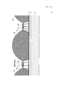
- FIG. 23 is a schematic cross-sectional view of an organic EL display panel having a line bank structure immediately after the coating process in the prior art.
- a depression 131 that is naturally formed by heat shrinkage is provided in advance at the top of the bank 13L.
- the amount of ink 8X applied to the element formation region is usually much larger than the inner volume of the recess 13L as shown in the figure. For this reason, when the substrate after ink application is transported from the inkjet apparatus, if the substrate is subjected to vibration or acceleration, the ink reservoir 10X held in the recess 131 can easily get over the recess 131 of the bank 13L. As shown in the figure, color mixing may occur with the adjacent ink 8X.
- the present invention has been made in view of the above problems, and an excellent image can be obtained by appropriately preventing the problem of color mixing caused by ink such as an organic light emitting material flowing into different element formation regions beyond a bank.
- ink such as an organic light emitting material flowing into different element formation regions beyond a bank.
- a coating type organic EL display panel that can be expected to have display performance and a method for manufacturing the same.
- an organic EL display panel which is one embodiment of the present invention includes a substrate, an interlayer insulating layer disposed to face the substrate, an interlayer insulating layer, and a row direction and a column direction.
- a first electrode provided corresponding to each of the plurality of element formation regions arranged along the row, a partition wall extending in the column direction so as to partition each element formation region arranged along the row direction,
- An organic light-emitting layer disposed to include organic light-emitting materials that have different emission colors in the element formation regions adjacent to each other in the row direction, the organic light-emitting layers disposed to face each organic light-emitting layer,
- a second electrode having a different polarity, and the interlayer insulating layer is provided with a first opening in accordance with a position between adjacent first electrodes in the row direction, and extends in the column direction Are buried between the first electrodes adjacent in the row direction and in the first opening, A body portion integrally formed by protruding from the portion, and the top portion of
- the embedded portion of the partition wall is embedded in the first opening formed between the first electrodes adjacent in the row direction and in the interlayer insulating layer (planarization film), and A first recess is formed at the top of the main body along the shape of the first opening and between the first electrodes adjacent in the row direction.
- the first recess is formed at a depth corresponding to the depth of the first opening. For example, if the depth of the first opening is adjusted in advance, the first recess having a sufficient depth is formed. Can be formed appropriately.
- the first dent portion is formed.
- the depth of can be adjusted significantly deeply and accurately.
- the ink overflowing from the element formation region has a sufficient depth even if vibration or acceleration accompanying conveyance or the like is applied to the substrate. It can hold
- the partition wall is firmly disposed on the substrate side by a so-called spike effect. Is done. For this reason, the edge part of the 1st electrode is pressed to the board
- the first electrode can be securely fixed.
- the buried portion is interposed between the adjacent first electrodes, the buried portion can reliably insulate the first electrodes from each other, and the operation reliability of the organic EL display panel can be expected to be improved.
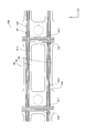
- FIG. 1 is a top view showing a configuration of an organic EL display panel (line bank structure) according to Embodiment 1.
- FIG. 3 is a partial enlarged view showing a configuration of an organic EL display panel according to Embodiment 1.
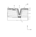
- FIG. 3 is a partial cross-sectional view showing a configuration of an organic EL display panel according to Embodiment 1.
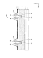
- FIG. 3 is an enlarged cross-sectional view showing a configuration around a contact hole of the organic EL display panel according to Embodiment 1.
- FIG. FIG. 6 is a partial cross-sectional view showing a configuration of an organic EL display panel (a coating type HIL layer) according to a second embodiment.
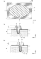
- FIG. 6 is a schematic top view showing a configuration of an organic EL display panel (line bank structure) according to a third embodiment and a partial cross-sectional view showing a configuration around a bank.
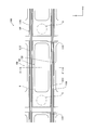
- FIG. 10 is a partial enlarged view showing a configuration of an organic EL display panel (line bank structure) according to a fourth embodiment.
- FIG. 10 is a partial enlarged view showing a configuration of an organic EL display panel (pixel bank structure) according to a fifth embodiment.
- FIG. 10 is a partial enlarged view showing a configuration of an organic EL display panel (pixel bank structure) according to a sixth embodiment.
- FIG. 10 is a partial cross-sectional view showing a configuration around a contact hole of an organic EL display panel (pixel bank structure) according to a seventh embodiment.
- FIG. 6 is a cross-sectional view for explaining the effect of Embodiment 1 (preventing ink color mixing). It is sectional drawing for demonstrating the conventional subject (ink color mixture generation
- An organic EL display panel includes a substrate, an interlayer insulating layer disposed to face the substrate, a plurality of element formation regions facing the interlayer insulating layer and arranged in the row direction and the column direction.
- the interlayer insulating layer is provided with a first opening in accordance with the position between the first electrodes adjacent in the row direction, and the partition wall extending in the column direction is between the first electrodes adjacent in the row direction.
- a buried portion of the partition wall is buried in the first opening formed between the first electrodes adjacent in the row direction and in the interlayer insulating layer (planarization film), A first recess is formed at the top of the main body along the shape of the first opening and between the first electrodes adjacent in the row direction. For this reason, since the depth of the first depression is adjusted according to the depth of the interlayer insulating layer, the first depression having a sufficient depth can be achieved by adjusting the depth of the first opening in advance. Can be formed.
- the depth of the recess can be set much deeper and more accurately than in the prior art, so that vibrations and accelerations associated with conveyance and the like are added to the substrate, and ink applied to the element formation region overflows. Ink overflowed in the first depression having a sufficient depth can be held well. Therefore, it is possible to manufacture an organic EL display panel satisfactorily while preventing color mixing between inks.
- the partition wall is firmly formed on the substrate side by the spike effect. Therefore, the end of the first electrode is pressed to the substrate side under the pressing force of the lower surface of the main body formed integrally with the embedded portion. As a result, the adhesion between the first electrode and the interlayer insulating layer is improved, and the first electrode is prevented from floating or peeling off the surface of the interlayer insulating layer, so that the first electrode can be reliably disposed. Furthermore, since the buried portion is interposed between the adjacent first electrodes, the first electrodes can be reliably insulated from each other, and improvement in operation reliability can be expected.
- the organic light emitting layer may be formed by applying an ink containing an organic light emitting material to the element formation region and drying the ink.
- the first depression formed in the main body can appropriately hold the ink overflowing from the element formation region, and the occurrence of ink color mixing is appropriate. Can be prevented.
- the partition walls extending in the column direction can be arranged in parallel in the row direction at predetermined intervals.
- each bank is sandwiched by providing the first depression at the top of the main body.
- the first recess may be formed along the column direction at the top of the main body of each partition wall.
- the first dent By forming the first dent in this manner, the first dent having a sufficient volume can be formed, so that the ink overflowing from the element formation region can be retained abundantly, and the ink color mixing can be further improved. Can be prevented.
- the partition may be extended in the column direction and the row direction so as to surround each element formation region.
- the interlayer insulating layer is provided with a second opening in accordance with the position between the first electrodes adjacent in the column direction, and is provided extending in the row direction.
- the partition wall includes a buried portion that is filled between adjacent element formation regions in the column direction and in the second opening, and a main body portion that is integrally formed by protruding from the buried portion.
- the top of each may have a configuration in which a second depression formed by depression along the shape of the second opening is present between element formation regions adjacent in the column direction.
- the organic EL display panel having the pixel bank structure by forming the depressions (the first depression and the second depression) with respect to the main body of any partition in the matrix direction, In addition to preventing color mixing of inks of different light emission colors, it is also possible to prevent the ink from flowing in any direction of the matrix in each element formation region, so that the effect of equalizing the amount of ink in each element formation region is also expected. it can.
- the first indented portion may have a higher lyophilic property than the surface of the main body portion surrounding the first indented portion.
- the second dent portion may be configured to have higher lyophilicity than the surface of the main body portion surrounding the second dent portion.
- the ink containing the organic light emitting material when at least one of the first depression and the second depression has lyophilicity, when the ink containing the organic light emitting material overflows into the depression, the ink is lyophilic.
- the ink wells are appropriately formed by being well adapted to the surface of the first depression or the second depression. As a result, abundant ink is held in the lyophilic first indentation or second indentation, and the occurrence of ink color mixture can be more effectively prevented.
- lyophilic refers to lyophilicity with respect to ink containing an organic light emitting layer material. Specifically, when the ink is water-based, “lyophilic” refers to “hydrophilic”.
- At least one of the first depression or the second depression has lyophilicity, and the surface of the other main body has relatively liquid repellency, so that the surface of the main body Ink can be prevented from adhering widely. For this reason, the ink can be satisfactorily held in the area surrounded by the adjacent partition walls, and the effect of preventing the ink from overflowing from the element forming area can be expected.
- one or more functional layers are provided between the first electrode and the organic light emitting layer, and the functional layer injects or transports charges.
- the charge injecting and transporting layer is stacked so as to be in direct contact with the first electrode, and is arranged so as to cover the first electrodes adjacent to each other in the row direction and the inner peripheral surface of the first opening. It can also be set as the structure provided.
- both the first electrode and the charge injecting and transporting layer are formed integrally with the embedded part by providing the embedded part of the partition wall inside the first opening.
- the lower surface of the main body is prevented from being lifted or peeled by being pressed toward the substrate side.
- one or a plurality of functional layers are provided between the first electrode and the organic light emitting layer, and the functional layer injects or transports charges.
- the partition may be arranged so as to be in contact with the first electrodes adjacent to each other in the row direction and the inner peripheral surface of the first opening.
- the charge injecting and transporting layer that is not in contact with the inside of the first opening can be formed by applying the material ink in the same manner as the organic light emitting layer.
- the first depression may have a depth corresponding to 10% or more and 100% or less of the height of the main body from the surface of the interlayer insulating layer.
- the second depression may have a depth corresponding to 10% or more and 100% or less of the height of the main body from the surface of the interlayer insulating layer.
- an interlayer insulating layer forming step for forming an interlayer insulating layer on the substrate, and a plurality of element forming regions arranged along the row direction and the column direction so as to face the interlayer insulating layer
- a second electrode forming step in which a second electrode having a different polarity is provided, wherein the interlayer insulating layer forming step includes a second electrode adjacent in the row direction based on a photoresist method.
- a first opening is provided in accordance with the position between one electrode.
- organic light emitting layers made of organic light emitting layer materials of different emission colors are disposed in adjacent element forming regions in the row direction, and in the partition forming step, the interlayer insulating layer is formed.
- the top part of the main body part is recessed between the first electrodes adjacent in the row direction and along the shape of the first opening part to form a first recess part.
- a lyophilic treatment may be performed so that the first dent portion has higher lyophilicity than the main body portion surrounding the dent portion. it can.
- the lyophilic process can be performed by a halftone exposure process or an ultraviolet irradiation process.
- the method includes a functional layer forming step of forming one or a plurality of functional layers on the upper surface of each first electrode between the first electrode disposing step and the partition forming step,
- the charge injecting and transporting layer which is a functional layer, is stacked in contact with the first electrode and covers the first electrodes adjacent in the row direction and the inner peripheral surface of the first opening. Can also be provided.
- an interlayer insulating layer forming step of forming an interlayer insulating layer on the substrate, and a plurality of element forming regions arranged along the row direction and the column direction so as to face the interlayer insulating layer A first electrode disposing step of providing a first electrode corresponding to each of the above, and a partition forming step of providing a partition extending in the column direction so as to partition each element forming region disposed along the row direction
- a second electrode forming step in which a second electrode having a different polarity is provided.
- a metal film is formed to face the interlayer insulating layer.
- a first opening is formed by excavating an interlayer insulating layer at a position between adjacent first electrodes in the row direction.
- an element forming region adjacent in the row direction is formed.
- organic light-emitting layers made of organic light-emitting layer materials of different emission colors are disposed, and in the partition forming step, the embedded portions are filled between the first electrodes adjacent to each other in the row direction and the first opening.
- a 1st hollow part can also be formed by hollowing along a shape.
- lyophilic treatment can be performed on the first dent so as to have higher lyophilicity than the main body surrounding the dent. .
- the lyophilic process can be performed by a halftone exposure process or an ultraviolet irradiation process.
- the method includes a functional layer forming step of forming one or a plurality of functional layers facing each first electrode between the first electrode disposing step and the partition forming step,
- charge injection as a functional layer is performed so as to be in contact with the first electrode and cover the first electrodes adjacent to each other along the row direction and the inner peripheral surface of the first opening.
- a transport layer can also be provided.
- FIG. 1 is a top view showing a configuration of a top emission type organic EL display panel 100 (hereinafter simply referred to as “panel 100”) according to Embodiment 1 of the present invention.
- FIG. 2 is a partially enlarged view around one organic EL element arranged on the panel 100.
- the configuration of the second electrode, the sealing layer, and the like disposed above the organic light emitting layer 8 is omitted for explanation.
- the outline of the first electrode 6 is indicated by a dotted line
- the outline of the contact hole 5 is indicated by a two-dot chain line.
- the organic EL elements 15R, 15G, and 15B are arranged in a matrix corresponding to the element formation regions arranged in the column (X) direction and the row (Y) direction. ing.
- organic EL elements 15 (15R, 15B, 15G) each having an organic light emitting layer 8 corresponding to any one of RGB emission colors are repeatedly arranged as subpixels.
- a combination of subpixels of three colors adjacent in the row (Y) direction functions as one pixel (pixel).
- reference numeral 20 shown in FIG. 1 denotes a sealing material disposed around the panel 100.
- a front panel (not shown) is overlaid on the panel 100 and attached using a sealing material 20.
- the panel 100 employs a so-called line bank structure, and banks 10L extending in a line shape in the column (X) direction are arranged side by side in a stripe shape in the row (Y) direction.
- a plurality of organic EL elements 15R, 15B, and 15G of the same color are arranged between each pair of adjacent banks 10L. Between adjacent pairs of banks 10L, adjacent organic EL elements 15 of the same color are partitioned by a pixel regulating layer 11 that forms a non-light emitting region as shown in FIG.
- FIG. 3 is a partial cross-sectional view of the panel 100 (a cross-sectional view taken along the line AA ′ in FIG. 2) showing a laminated structure around one organic EL element.
- 4 is a partial cross-sectional view of the panel 100 (a cross-sectional view taken along line BB ′ in FIG. 2).
- the panel 100 includes a TFT wiring portion (TFT layer) 2 and a planarization film (interlayer insulating layer) with respect to one side main surface of the TFT substrate 1 (hereinafter simply referred to as “substrate 1”). 4, a first electrode (anode) 6 and a charge injection / transport layer 7 are sequentially laminated.
- the bank 10L is formed on the surface of the charge injection / transport layer 7 in the panel 100. However, when the charge injection / transport layer 7 is provided after the bank 10L is laminated, or when the charge injection / transport layer 7 is not provided, the bank 10L is flat. The bank 10L can also be provided directly on the conversion film 4.
- an organic light emitting layer 8 In an element formation region between a pair of adjacent banks 10L, an organic light emitting layer 8, a second electrode (cathode) (not shown), and a sealing resin are sequentially stacked on the surface of the charge injection / transport layer 7.
- the substrate 1 is a base portion of the panel 100, and includes alkali-free glass, soda glass, non-fluorescent glass, phosphoric acid glass, boric acid glass, quartz, acrylic resin, styrene resin, polycarbonate resin, epoxy resin, polyethylene, It can be formed using any known material such as polyester, silicone resin, or insulating material such as alumina.
- the TFT wiring part 2 is formed on the surface of the substrate 1 in order to drive all the organic EL elements 15R, 15G, and 15B arranged on the panel 100 by an active matrix method.
- the planarizing film (interlayer insulating layer) 4 is made of an organic material such as polyimide having excellent heat resistance and insulating properties, and covers a portion of the TFT wiring portion 2 excluding the feeding electrode (transparent electrode portion) 3 so as to cover the substrate surface. Is arranged to flatten the surface. As shown in FIG. 4, the planarizing film 4 has a circular bottom surface formed by digging down the corresponding portion along the thickness (Z) direction in order to expose the power supply electrode 3 and make an electrical connection with the lower electrode 6. A hole (contact hole 5) is formed.
- two or more contact holes 5 can be provided in one element formation region.
- a shape it is not limited to the shape which has a circular bottom face like FIG. 2, The shape which has a polygonal bottom face may be sufficient.
- the planarizing film 4 has a certain depth at a position corresponding to the position between the first electrodes 6 and 6 adjacent to each other in the row (Y) direction, which is the arrangement position of the bank 10L.
- a deepened opening 41 is formed.
- the opening 41 is formed as a groove along the column (X) direction.
- the first electrode 6 is a strip-shaped electrode (anode) having a certain length, and is arranged in a matrix for each element formation region with the column (X) direction as the longitudinal direction as shown in FIGS.
- the Each first electrode 6 is configured by laminating a transparent conductive film on the surface of a reflective metal film. Most of the lower surface of the first electrode 6 is in contact with the surface of the planarizing film 4, but a part of the first electrode 6 enters the contact hole 5 and is electrically connected to the power supply electrode 3.
- the reflective metal film is a metal material (aluminum or aluminum alloy) having a good visible light reflectance so as to supply power to the organic light emitting layer side and to efficiently extract light generated in the organic light emitting layer 8 from above.
- the “aluminum alloy” here refers to an alloy obtained by adding at least one of iron, copper, manganese, zinc, nickel, magnesium, palladium, cobalt, and neodymium to aluminum.
- the transparent conductive film is made of a known transparent conductive material such as ITO or IZO, covers the reflective metal film, shields the reflective metal film from oxygen in the atmosphere, and reflects the reflective metal film by forming an unnecessary film. The rate and conductivity are prevented from decreasing.
- the pixel regulation layer (PCL) 11 is a layer made of an insulating material such as SiON, and as shown in FIGS. 1 and 2, charge injection transport between adjacent element formation regions along the column (X) direction. On the surface of the layer 7, it is formed so as to be orthogonal to the longitudinal (X) direction of the bank 10L.
- the region where the pixel restricting layer 11 is provided becomes a non-light emitting region (so-called pixel restricting region) when the first electrode 6 or the second electrode (not shown) is cut off from the light emitting layer 8 during driving.
- the charge injecting and transporting layer 7 is one of functional layers provided between the first electrode 6 and the organic light emitting layer 8, and efficiently transports charges (holes) supplied from the anode side during driving to produce organic light emission. It is provided for injection into the layer 8 side. Examples of materials include known materials such as (molybdenum and tungsten oxides).
- the charge injecting and transporting layer 7 is disposed here by vapor deposition. In this case, as shown in FIG. 3, the first electrodes 6 are stacked so as to be in direct contact with each other and cover the inner peripheral surface of the first opening 41 of the planarizing film 4 between the adjacent first electrodes in the row direction. It is provided as follows.
- the functional layer is provided as a laminate of one or more layers between the first electrode and the organic light emitting layer 8. For this reason, another functional layer may be laminated in addition to the charge injecting and transporting layer 7. Instead of the charge injection / transport layer 7, two functional layers of the charge injection layer and the charge transport layer may be laminated in the same order from the surface side of the first electrode 6.
- the organic light emitting layer 8 is configured by applying an ink containing a predetermined organic light emitting material corresponding to one of RGB emission colors to the surface of the charge injection transport layer 7 and drying it.
- a known material can be used.
- the bank (partition wall) 10L is made of an insulating organic material (for example, acrylic resin, polyimide resin, novolac type phenol resin, etc.), and is arranged in a row so as to partition between adjacent element formation regions in the row (Y) direction.
- X) is stretched in a line along the direction, and is arranged in parallel in the row (Y) direction at regular intervals.
- the bank 10 ⁇ / b> L is embedded by embedding a bank material between the first electrodes 6 adjacent in the row (Y) direction and the first openings 41 formed in the planarization film 4. And a main body portion 103 that is raised above the embedded portion 102.
- the bank material forming the embedded portion 102 is dropped into the top portion of the main body portion 103 between the first electrodes 6 adjacent in the row (Y) direction and the inside of the first opening 41 of the planarizing film 4. As a result of the depression, the depression 101 is formed.
- the hollow portion 101 is a groove formed in a line shape along the longitudinal direction (column (X) direction) of the bank 10L as a whole.
- the depression 101 is overflowed from the element forming region.
- the ink is appropriately held and disposed for the purpose of preventing the inks from mixing with each other between the element formation regions of different emission colors separated from the bank 10L.
- the inner surface of the depression 101 is subjected to a lyophilic process so that the ink overflowing from the element formation region can be satisfactorily retained as the ink reservoir 9X (see FIG. 22).
- the surface of the main body 103 excluding the depression 101 is water-repellent so that the ink can be dried with a uniform coating film in the element formation region.
- the depth (the amount of the hollow portion) of the hollow portion 101 is proportional to the depth of the opening portion 41.
- the depth of the depression 101 is desirably a sufficient depth to appropriately hold the overflowed ink. For example, it is appropriate to set the depth corresponding to a value of 10% to 100% of the height of the main body from the surface of the planarizing film 4.
- the second electrode (cathode) laminated on the organic light emitting layer 8 is made of, for example, ITO (indium tin oxide), IZO (indium zinc oxide), or the like. Since the panel 100 has a top emission type structure, it is necessary to use a light transmissive material as a material of the second electrode.
- a known sealing layer is provided on the second electrode.
- the sealing layer is formed of a material such as SiN (silicon nitride) or SiON (silicon oxynitride), for example, and suppresses deterioration of the organic light emitting layer 8 due to contact with moisture or air.
- This sealing layer is also made of a light transmissive material.
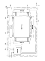
- FIG. 21 is a diagram illustrating a configuration of a display device 200 using the panel 100.
- the display device 200 includes a panel 100 and a drive control unit 120 connected thereto.
- the drive control unit 120 includes four drive circuits 121 to 124 and a control circuit 125.
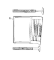
- FIG. 22 is an external shape showing an example of a television system using the display device 200. (About various effects which the panel 100 has)
- the organic light emitting layer 8 disposed in each of the organic EL elements 15R to 15B and having a different emission color uses the recess 101 of the bank 10L in the manufacturing process, thereby providing an organic light emitting material.
- the ink containing the ink is applied, color formation is prevented and it is formed well, and has excellent image display performance.
- the organic light emitting layer 8 is usually formed by applying an ink containing an organic material and a solvent and evaporating and drying the solvent component in an application process by an ink jet method.
- the depression 101 is not simply formed by utilizing the volume shrinkage at the time of baking the bank 10L, but between the opening 41 of the planarization film 4 and the first electrode 6 adjacent in the row (Y) direction. It is formed to have a sufficient depth (volume) according to the shape. For this reason, as shown in FIG. 22, even if a large amount of ink applied to each element formation region overflows to the outside due to acceleration or vibration accompanying the conveyance of the substrate, it has a sufficient depth (volume). It flows into the depression 101 and is appropriately retained as a liquid pool 9X.
- the ink As a result, it is possible to prevent the ink from overcoming the bank 10L and flowing into other element formation regions. Therefore, it is possible to prevent color mixing between the inks having different emission colors applied across the bank 10L.
- the organic light emitting layer 8 is formed well, and the panel 100 having excellent image display performance is realized.
- a buried portion 102 is disposed in an opening 41 having a sufficient depth formed in the planarizing film 4 between the first electrodes 6 and 6 adjacent in the row (Y) direction. Yes.
- the bank 10L is firmly arranged on the substrate side by a so-called spike effect, so that the pressing force from the lower surface portion (surface portion along the substrate 1) of the main body portion 103 formed integrally with the embedded portion 102 is reduced.
- the end portions of the first electrode 6 and the charge injecting and transporting layer 7 are pressed toward the substrate side.
- the first electrode 6 (charge injection transport layer 7) is prevented from being lifted or peeled off from the surface of the planarization film 4 (first electrode 6), and the first electrode 6 and the planarization film 4,
- Each adhesiveness of the 1st electrode 6 and the electric charge injection transport layer 7 can be improved, and these can be arrange
- the charge injection / transport layer 7 is covered on the inner peripheral surface of the opening 41, and accordingly, the buried portion 102 can ensure a wide contact area with the charge injection / transport layer 7. For this reason, the charge injecting and transporting layer 7 can stably maintain a state in which the charge injecting and transporting layer 7 is in good contact with both the embedded portion 102 and the first electrode 6.
- the panel 100 has a configuration in which the buried portion 102 is interposed between the first electrodes 6 and 6 adjacent in the row (Y) direction, so that the first electrodes 6 and 6 can be reliably insulated from each other, and the operation reliability can be improved. We can expect improvement.
- Such a depression 101 can be formed to have a sufficient depth and shape by adjusting the depth of the opening 41 formed in the planarization film 4. Details of the adjustment of the depth of the recess 101 will be discussed later.
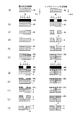
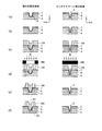
- FIGS. Metal for manufacturing organic EL display panel 100
- FIGS. An overall manufacturing method of the organic EL display panel 100 will be exemplified with reference to FIGS.
- illustration of the substrate 1, the TFT layer 2, and the power supply electrode 3 is omitted for simplification of explanation.
- 11 to 13 YZ sectional views of the peripheral region of the bank 10L (recessed portion) 101 are shown on the left side in the drawing. Further, on the right side of the drawing, an XZ sectional view of the peripheral region of the contact hole 5 is shown.
- the panels 100A to 100E can be basically manufactured in the same manner.
- Board preparation process First, the substrate 1 is prepared and placed in the chamber of the sputter deposition apparatus. Then, a predetermined sputtering gas is introduced into the chamber, and the TFT layer 2 and the feeding electrode 3 are formed based on the reactive sputtering method as shown in FIG.
- planarizing film forming step; first method Next, based on the photoresist method, an organic material (planarization film material 4X) containing a well-known photo-curing resin having an excellent insulating property facing the TFT layer 2 and the feeding electrode 3 and having a final thickness of about 4 ⁇ m. (FIG. 11 (a)).
- a predetermined photomask PM1 is disposed opposite to the surface of the applied planarization film material 4X.
- a halftone window is disposed in a portion where the opening 41 is formed, and an opening window is disposed in a portion where the contact hole 5 is formed.
- an exposure process is performed from the outside (FIG. 11B).
- development processing is performed, a recess having a certain depth is formed in a portion where the opening 41 is formed, and an opening is formed in a portion where the contact hole 5 is formed (FIG. 11C).
- the halftone window is a means for adjusting the depth of the opening, and the depth of the opening can be deeply adjusted by increasing the exposure amount of the halftone window.
- the transmittance of the halftone window of the photomask PM1 the transmittance
- the planarization film 4 can be formed in the same manner as described above by adjusting the depth and shape of the opening 41 to be formed in advance. (First electrode forming step; first method) Subsequently, a metal film 6X having a thickness of about 50 nm is uniformly formed on the planarizing film 4 on the basis of a vacuum deposition method or a sputtering method (FIG. 11E).
- a resist PR1 containing a photodegradable resin is uniformly applied so as to face this (FIG. 11 (f)), and exposure is performed through a photomask PM2 having an opening window at a position corresponding to the opening 41.
- Process FIG. 11 (g)
- the resist PR1 at a position corresponding to the opening 41 is peeled off.
- Etching is performed in this state (FIG. 11 (i)), and if the remaining resist PR1 is peeled off, the end of the metal film 61X facing the opening 41 is cut off so that the inside of the contact hole 5 is covered.
- the provided first electrode 6 is completed (FIG. 11 (j)).
- the following 2nd method can also be taken as a planarization film
- the surface of the flattened film 4 once formed flat is etched in accordance with the patterning of the first electrode 6 to provide an opening 41.
- the planarizing film material 4X is uniformly applied so as to face the TFT layer 2 and the feeding electrode 3 so that the final thickness is about 4 ⁇ m.
- the resist PR1 is uniformly formed thereon, and the exposure process is performed through the photomask PM2 (see FIG. 11E).
- the metal film 6X at the position where the opening 41 is formed is exposed (FIG. 12H).
- a first etching process (wet etching) is performed, and the metal film 6X is patterned to form the first electrode 6 (FIG. 12 (i)).
- a second etching process (wet etching or dry etching) is performed, and the exposed planarizing film 4 is excavated in the thickness direction (FIG.
- the depth of the opening can be increased in proportion to the strength and processing time of the second etching process.
- the process proceeds to the functional layer forming step.
- an inorganic oxide (insulator) such as SiON is uniformly formed facing the substrate surface by a method such as vacuum deposition.
- the photoresist method uses the photoresist method on the surface of the inorganic oxide, the pixel regulation layer 11 is formed between the element formation regions adjacent in the column (X) direction.
- a resist material containing a photodegradable resin is uniformly applied facing the substrate surface on which the functional layer is formed.
- a photomask is provided so as to arrange an opening window at a position other than the position corresponding to the element formation region, and an exposure process is performed.
- a development process is performed, a resist film is formed along the row (Y) direction so as to expose a region other than between the element formation regions.
- a charge injecting and transporting layer 7 is formed as a functional layer so as to face the upper surface of the first electrode 6.
- film formation based on the reactive sputtering method is performed.
- a metal material such as molybdenum or tungsten is used as a sputtering source (target), and argon gas as a sputtering gas and oxygen gas as a reactive gas are introduced into the chamber, respectively, to form a film (FIG. 13A).
- a charge injection / transport layer 7 made of an oxide of molybdenum or tungsten is formed (FIG. 13B).
- the charge injection / transport layer 7 is uniformly formed on the inner peripheral surface of the opening 41 and the surface of the first electrode 6 in the contact hole 5.
- the bank material for example, a fluorine-based or acrylic-based resist material containing a photocurable resin is prepared. This is applied uniformly across the surface of the charge injecting and transporting layer 7 (FIG. 13C). At this time, the resist material applied to the opening 41 and the contact hole 5 falls along the shape of the opening 41 and the contact hole 5 (FIG. 13C).
- a photomask PM3 is disposed on the applied resist material 10X, and an exposure process is performed so that light is irradiated to a position corresponding to the opening 41 through the opening window (FIG. 13D). Thereafter, by performing development processing, the resist material 10X other than the position corresponding to the opening 41 is removed (FIG. 13E) After that, when baking processing is performed, the embedded portion 102, the main body portion 103, and the depression A line-shaped bank 10L having the portion 101 is completed (FIG. 13F).
- the bank material falls along the openings 41 having the predetermined depth and shape formed earlier (FIG. 13C), and the predetermined depressions 101 and 101X are formed. , 101Y, etc., banks 10P, 10L are formed.
- a resist PR2 containing a photodegradable resin is applied to the surface of the bank 10L formed so as to face the pair (FIG. 14A).
- a photomask PM4 having an opening window is disposed at a position corresponding to the recess 101, and exposure processing is performed (FIG. 14B). Thereafter, development processing is performed to remove the uncured resist, so that only the hollow portion 101 is exposed to the outside (FIG. 14C).
- ultraviolet irradiation for example, 1000 mJ irradiation using high-pressure mercury or the like
- the resist PR2 is removed, and the processing is completed (FIG. 14E).
- the lyophilic process performed to the hollow part 101 is not limited to this.
- an ink containing an organic light emitting layer material is applied using an inkjet apparatus system (printing apparatus).
- FIG. 15 is a schematic view showing a coating process (organic light emitting layer forming process). In the figure, the progress of the process is shown from the left side to the right side.
- an organic material which is an organic light emitting layer material, and a solvent are mixed at a predetermined ratio to prepare ink.
- This ink is supplied to the ink jet head of the ink jet apparatus system shown in FIG.
- the application target substrate is placed on the stage of the printing apparatus.
- an ink jet head disposed on an XY arm is scanned to apply ink so as to face the charge injection transport layer 7 in each element formation region (FIG. 15A). )).
- This coating process is performed in the same manner over all element formation regions finally disposed on the substrate by sequentially refilling three types of inks having different emission colors.
- the lift-up pin is actuated to lower the application target substrate from the stage of the printing apparatus (FIG. 15B).
- the substrate to be coated is transported into the drying apparatus by horizontal transport using a robot arm or a roller, and the substrate to be coated is placed on a hot plate in the chamber.
- the inside of the chamber is set to a nitrogen atmosphere or a vacuum (reduced pressure) atmosphere, and the ink is dried (FIG. 15C).
- the substrate is transferred to a baking apparatus by horizontal transfer using a robot arm or a roller, and a baking process is performed in a nitrogen atmosphere or a vacuum (decompressed) atmosphere to complete the organic light emitting layer 8.
- the application target substrate on which the ink application has been completed is transported from the stage of the printing apparatus to the drying apparatus, vibration and acceleration are applied to the substrate, and the applied ink may overflow from a predetermined element formation region.
- the depression 101 having a sufficient depth (volume) is formed at the top of the bank 10L, even if the ink 8X is in the row (Y Even if the ink overflows in the direction), the ink becomes an ink reservoir 9X inside the depression 101 and is appropriately held. For this reason, it is possible to prevent the color mixing of inks that can occur between the element forming regions coated with inks having different emission colors, and to form the organic light emitting layer satisfactorily.
- the surface of the main body portion 103 excluding the recess portion 101 has a relatively liquid repellency compared to the recess portion 101, thereby preventing ink from adhering widely to the surface of the main body portion 103. Is done. Therefore, since the ink can be satisfactorily held between a pair of adjacent banks 10L, an effect of preventing the ink from overflowing from the element formation region can be expected.
- a film such as ITO, IZO or the like is used and deposited by a vacuum deposition method so as to face the surface of each of the formed organic light emitting layers 8. Thereby, the second electrode 10 is formed.
- a sealing layer is formed on the surface of the second electrode 10 by depositing a material such as SiN (silicon nitride) or SiON (silicon oxynitride) by a vacuum deposition method.
- FIG. 5 is a partial cross-sectional view of panel 100A according to Embodiment 2 (corresponding to FIG. 3 related to panel 100).
- the panel 100A is characterized in that the charge injecting and transporting layer 7 is formed using an organic material such as PEDOT (polyethylenedioxythiophene) and disposed as a coating type. That is, the charge injecting and transporting layer 7 of the panel 100A is formed by applying ink to the surface of the first electrode 6 between adjacent banks 10L and drying it in the functional layer forming step.
- the embedded portion 102 of the bank 10 ⁇ / b> L is disposed so as to be in direct contact with each side surface of the adjacent first electrode 6 and the inner peripheral surface of the opening 41 of the planarizing film 4.
- FIG. 6A is a schematic front view showing the configuration of panel 100B according to the third exemplary embodiment.
- the amount of depression of the bank 10L in the panel peripheral region indicated by “B” is adjusted to be larger than the amount of depression of the bank 10L in the panel central region indicated by “A”.
- the panel peripheral area B has an in-plane distribution in which ink color mixing is relatively easy compared to the panel central area A.
- the reason for this is that, after applying ink to the panel, when the substrate to be applied is moved and transported, the angle with respect to the horizontal direction is relatively likely to fluctuate in the panel peripheral region B. The reason is that it is easy to induce overflow.
- the panel 100B takes this problem into consideration, and as shown in FIG. 6B, in the panel central region A, the depth of the embedded portion 102 is D1, and the depth of the recessed portion 101 (the amount of the recessed portion) is H1. Set. On the other hand, in the panel peripheral region B, as shown in FIG. 6C, the depth D2 of the embedded portion 102 is set to be deeper than D1, and the hollow portion 101 having a sufficient depth H2 is formed. As an example of setting numerical values, when D1 is 1000 nm, H1 can be set to about 250 nm. When D2 is 3000 nm, H2 can be set to about 750 nm.
- Such adjustment methods for H1, H2, D1, and D2 are such that, for example, in the above-described planarization film forming process, the light transmission is performed so that the exposure amount for the planarization film material 4X differs between the panel central region A and the peripheral region B. This can be done by performing an exposure process using a predetermined halftone mask (photomask PM1) whose rate is adjusted.
- photomask PM1 a predetermined halftone mask
- the depths D ⁇ b> 1 and D ⁇ b> 2 of the embedded portion 102 are actually the sum of the depth of the opening 41 of the planarizing film 4 and the thicknesses of the first electrode 6 and the charge injection / transport layer 7. It corresponds to. However, since the thickness of the planarization film 4 is normally sufficiently thick with respect to the thicknesses of the first electrode 6 and the charge injecting and transporting layer 7, the thickness of the planarization film 4 is adjusted in adjusting the depth of the buried portion 102. Conditions seem to be dominant.
- the pattern of the central region A provided on the panel 100B is not limited to the elliptical shape shown in FIG. 6A of the front view, and may be another pattern (for example, a rectangular pattern).
- the minimum widths L1 and R1 of the peripheral region B can also be changed.
- the minimum width L1 is in the range of 10% to 20% of the length in the row (Y) direction of the panel 100B
- the minimum width R1 is the column (X ) It can be appropriately set in the range of 10% to 20% of the direction length.
- FIG. 7 is a partially enlarged view around the element in the panel 100C according to the fourth embodiment (corresponding to FIG. 2 showing the panel 100).
- the bank 10L of the panel 100C is provided with a long recess 101 intermittently in accordance with the position of each element formation region.
- the arrangement position of the depression 101 corresponds to the light emitting region of each organic EL element 15R, 15G, 15B (that is, a region where no pixel restricting layer is provided).
- FIG. 8 is a partial enlarged view of the periphery of the element of panel 100D according to Embodiment 5 (corresponding to FIG. 2 relating to panel 100).
- the panel 100D has a so-called pixel bank structure, and bank portions 110X and 110Y are arranged along the matrix direction so as to surround each element formation region, thereby forming a cross-shaped bank 10P.
- the bank part 110X has substantially the same configuration as the bank 10L of the first embodiment, and is configured by forming a main body part on a buried part (not shown), along the row (X) direction on the top part of the main body part.
- FIG. 9 is a partial enlarged view (corresponding to FIG. 2 related to the panel 100) around the element of the panel 100E according to the sixth embodiment.
- Panel 100E is based on panel 100D of the fifth embodiment, and has a configuration in which depressions 101Y are formed along the row (Y) direction with respect to the top of bank unit 110Y.
- FIG. 10 is a cross-sectional view (corresponding to FIG. 3 related to the panel 100) around the contact hole of the panel 100F according to the seventh embodiment.
- the panel 100F has substantially the same configuration as the panel E, but the main feature is that the X-direction width of the main body 104 in the bank 110Y extending in the row (Y) direction is expanded to the region including the contact hole 5.
- the same effect as that of the panel 100E can be obtained, and by having the wide bank portion 110Y, the ink applied to each element formation region can be applied to other element formation regions adjacent in the column (X) direction. Inflow is effectively suppressed, which is advantageous in forming the organic light emitting layer 8 having a uniform film thickness.
- the bank portion 110Y can be patterned together with the structure around the contact hole, the bank patterning in the bank formation process can be performed relatively easily, and the panel 100F can be manufactured with good manufacturing efficiency. ⁇ About the depth of the recess> Next, the relationship between the depth of the opening of the planarizing film (the amount of depression) and the depth of the depression of the bank formed thereby will be described.
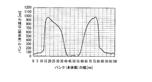
- FIG. 16 is a graph showing the relationship between the depth of the opening (dent amount) formed in the planarizing film and the depth of the recess of the bank.
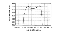
- 17 to 19 are measurement diagrams showing the cross-sectional shape of the bank when the recess of the opening of the planarizing film is changed. The amount of recess in the opening was adjusted by changing the exposure amount using a known halftone mask after a flattening film was uniformly formed.
- the depth of the recess in the main body is in a substantially linear proportional relationship with the amount of recess in the opening of the planarizing film.
- the depth of the recess can be adjusted in proportion to the depth of the opening.
- the amount of depression in the opening does not directly become the depth of the depression in the main body, but has a slight opening (straight line in FIG. 16). It is considered that the relationship between the amount of depression in the opening and the depth of the depression in the main body varies depending on the type and characteristics (viscosity, hardness, etc.) of the resist material used for the bank.
- FIG. 19 shows data using the contact hole peripheral structure instead of the opening, but it seems that the same result can be obtained even if the opening is used.
- the organic light emitting layer 8 is exemplified by a configuration (coating type) obtained by applying ink and drying it, but the organic light emitting layer is not limited to the coating type and may be formed by other methods. For example, it can be formed by a so-called vacuum process using a vacuum deposition method, a sputtering method, an electron beam method, or the like.
- the effect of preventing color mixing of ink is irrelevant, but the bank 10L is formed by the embedded portion 103 and the main body portion 102 embedded in the opening 41, so that the first electrode 6 and the electric charges are formed on the lower surface of the main body portion 102. It is possible to expect the effect of suppressing the injection transport layer 7 and the like to the substrate side and appropriately preventing peeling and lifting. Moreover, the effect of reliably preventing the short-circuit between the adjacent first electrodes 6 and 6 by the interposition of the embedded portion 103 is also achieved.
- the “row direction” and the “column direction” referred to in the present invention are exemplary directions that indicate two directions orthogonal to each other along the surface of the organic EL display panel. Accordingly, the notation of “row direction” and “column direction” described in this specification is not strictly strict, and these directions may be interchanged.
- the present invention can be used as a display device for a mobile phone, a display device such as a television, an organic EL device used for various light sources, an organic EL display panel using the same, and a manufacturing method thereof.
- a display device such as a television
- an organic EL device used for various light sources such as a television
- an organic EL display panel using the same such as a television
- a manufacturing method thereof it is possible to expect an organic EL element or an organic EL display panel that can exhibit good light emission characteristics or image display performance with little display unevenness.
Landscapes
- Engineering & Computer Science (AREA)
- Microelectronics & Electronic Packaging (AREA)
- Physics & Mathematics (AREA)
- Optics & Photonics (AREA)
- Manufacturing & Machinery (AREA)
- Electroluminescent Light Sources (AREA)
Abstract
L'invention porte sur un panneau d'affichage électroluminescent organique du type à revêtement et sur son procédé de production, dans lequel d'excellentes performances d'affichage d'image peuvent être espérées par prévention adéquate de problèmes selon lesquels de l'encre formée à partir d'un matériau électroluminescent organique passe par-dessus la rive pour couler dans une région de formation d'élément différente, provoquant un mélange de couleurs. Spécifiquement, une section d'ouverture (41) est formée sur un film de planarisation (4), une section encastrée (102) est encastrée dans la section d'ouverture (41), et une rive (10L) est formée par formation monobloc d'une section de corps principal (103) avec la section encastrée (102). Une section renfoncée (101) ayant une profondeur suffisante est formée sur le dessus de la section de corps principal (103) en accord avec la forme de la section d'ouverture (41) et entre des premières électrodes (6) qui sont voisines l'une de l'autre dans la direction des rangées (Y). Lorsqu'une encre contenant un matériau électroluminescent organique est déposée en couche, de l'encre qui déborde de la région de formation d'élément est retenue par la section renfoncée (101), ce qui empêche un mélange de la couleur de l'encre.
Priority Applications (3)
| Application Number | Priority Date | Filing Date | Title |
|---|---|---|---|
| PCT/JP2010/004988 WO2012017498A1 (fr) | 2010-08-06 | 2010-08-06 | Panneau d'affichage électroluminescent organique et son procédé de production |
| JP2012527475A JP5677435B2 (ja) | 2010-08-06 | 2010-08-06 | 有機el表示パネルとその製造方法 |
| US13/709,445 US8816339B2 (en) | 2010-08-06 | 2012-12-10 | Organic EL display panel, and method for producing same |
Applications Claiming Priority (1)
| Application Number | Priority Date | Filing Date | Title |
|---|---|---|---|
| PCT/JP2010/004988 WO2012017498A1 (fr) | 2010-08-06 | 2010-08-06 | Panneau d'affichage électroluminescent organique et son procédé de production |
Related Child Applications (1)
| Application Number | Title | Priority Date | Filing Date |
|---|---|---|---|
| US13/709,445 Continuation US8816339B2 (en) | 2010-08-06 | 2012-12-10 | Organic EL display panel, and method for producing same |
Publications (1)
| Publication Number | Publication Date |
|---|---|
| WO2012017498A1 true WO2012017498A1 (fr) | 2012-02-09 |
Family
ID=45559031
Family Applications (1)
| Application Number | Title | Priority Date | Filing Date |
|---|---|---|---|
| PCT/JP2010/004988 Ceased WO2012017498A1 (fr) | 2010-08-06 | 2010-08-06 | Panneau d'affichage électroluminescent organique et son procédé de production |
Country Status (3)
| Country | Link |
|---|---|
| US (1) | US8816339B2 (fr) |
| JP (1) | JP5677435B2 (fr) |
| WO (1) | WO2012017498A1 (fr) |
Cited By (13)
| Publication number | Priority date | Publication date | Assignee | Title |
|---|---|---|---|---|
| WO2014020914A1 (fr) * | 2012-08-02 | 2014-02-06 | パナソニック株式会社 | Panneau d'affichage el organique et son procédé de fabrication |
| CN103889087A (zh) * | 2012-12-21 | 2014-06-25 | 株式会社半导体能源研究所 | 发光装置及其制造方法 |
| US20150263284A1 (en) * | 2012-06-21 | 2015-09-17 | Osram Oled Gmbh | Method for closely connecting an organic optoelectronic component to a connection piece, connection structure for force-locking connecting, and optoelectronic component device |
| JP2016085923A (ja) * | 2014-10-28 | 2016-05-19 | パイオニア株式会社 | 発光装置 |
| KR20160129188A (ko) * | 2015-04-29 | 2016-11-09 | 삼성디스플레이 주식회사 | 유기 발광 표시 장치 |
| KR20180013469A (ko) * | 2016-07-29 | 2018-02-07 | 엘지디스플레이 주식회사 | 유기발광다이오드 표시장치 |
| CN108878472A (zh) * | 2017-05-12 | 2018-11-23 | 京东方科技集团股份有限公司 | 一种oled显示基板及其制作方法、显示装置 |
| CN110010778A (zh) * | 2017-12-14 | 2019-07-12 | 乐金显示有限公司 | 电致发光显示设备 |
| JP2019133959A (ja) * | 2019-05-21 | 2019-08-08 | パイオニア株式会社 | 発光装置 |
| JP2021039956A (ja) * | 2020-12-08 | 2021-03-11 | パイオニア株式会社 | 発光装置 |
| WO2021213439A1 (fr) * | 2020-04-21 | 2021-10-28 | 京东方科技集团股份有限公司 | Dispositif d'affichage, et panneau d'affichage et procédé de fabrication associés |
| KR20220103079A (ko) * | 2015-02-06 | 2022-07-21 | 삼성디스플레이 주식회사 | 디스플레이 장치 및 이의 제조 방법 |
| WO2023133916A1 (fr) * | 2022-01-13 | 2023-07-20 | 深圳市华星光电半导体显示技术有限公司 | Panneau d'affichage souple et son procédé de fabrication |
Families Citing this family (25)
| Publication number | Priority date | Publication date | Assignee | Title |
|---|---|---|---|---|
| WO2012168974A1 (fr) | 2011-06-08 | 2012-12-13 | パナソニック株式会社 | Panneau électroluminescent, procédé de fabrication de panneau électroluminescent, et système de dépôt de pellicule |
| JP6135427B2 (ja) * | 2013-09-27 | 2017-05-31 | 凸版印刷株式会社 | 薄膜トランジスタアレイおよびその製造方法 |
| KR102201827B1 (ko) * | 2014-09-16 | 2021-01-13 | 엘지디스플레이 주식회사 | 유기발광표시장치, 유기발광표시패널 및 그 제조방법 |
| CN104882468B (zh) | 2015-06-09 | 2017-12-15 | 京东方科技集团股份有限公司 | 有机电致发光显示基板及其制作方法、显示装置 |
| CN105140236B (zh) * | 2015-07-31 | 2019-08-06 | 京东方科技集团股份有限公司 | 基板组件及其制备方法以及显示装置 |
| CN108022942B (zh) * | 2016-10-31 | 2020-06-30 | 上海和辉光电有限公司 | 一种阵列基板和有机发光显示面板 |
| KR102546420B1 (ko) * | 2016-11-11 | 2023-06-22 | 엘지디스플레이 주식회사 | 전계발광 표시장치 및 그 제조방법 |
| CN108074950B (zh) * | 2016-11-11 | 2021-11-23 | 乐金显示有限公司 | 电致发光显示设备及其制造方法 |
| CN108074951A (zh) * | 2016-11-14 | 2018-05-25 | 上海和辉光电有限公司 | 一种有机发光面板 |
| KR102676858B1 (ko) * | 2016-12-16 | 2024-06-19 | 엘지디스플레이 주식회사 | 전계발광 표시장치 |
| CN108364987B (zh) * | 2018-02-24 | 2021-01-26 | 京东方科技集团股份有限公司 | 显示基板及其制备方法、显示装置 |
| JP7076135B2 (ja) * | 2018-07-27 | 2022-05-27 | 株式会社Joled | 有機el表示パネルの製造方法 |
| CN109148533B (zh) * | 2018-08-21 | 2020-09-01 | 武汉华星光电半导体显示技术有限公司 | 一种有机发光二极管显示器 |
| KR102693172B1 (ko) * | 2018-09-28 | 2024-08-07 | 엘지디스플레이 주식회사 | 표시장치 |
| KR102919190B1 (ko) | 2019-05-21 | 2026-01-30 | 삼성디스플레이 주식회사 | 표시 패널 및 이의 제조 방법 |
| CN110112203B (zh) * | 2019-05-30 | 2021-04-16 | 京东方科技集团股份有限公司 | 显示背板及其制备方法和显示装置 |
| CN110224010B (zh) * | 2019-06-13 | 2021-04-27 | 京东方科技集团股份有限公司 | Oled显示基板、显示面板、oled显示基板的制备方法 |
| CN110534548A (zh) * | 2019-08-06 | 2019-12-03 | 武汉华星光电半导体显示技术有限公司 | Oled显示面板 |
| CN110993646B (zh) * | 2019-11-08 | 2022-07-12 | 深圳市华星光电半导体显示技术有限公司 | Oled背板的制备方法及oled背板 |
| US12089451B2 (en) | 2019-12-25 | 2024-09-10 | Semiconductor Energy Laboratory Co., Ltd. | Functional panel, display device, input/output device, and data processing device |
| CN111192905A (zh) * | 2020-01-08 | 2020-05-22 | 武汉华星光电半导体显示技术有限公司 | 有机发光二极体显示器件及其制造方法 |
| US11424270B2 (en) * | 2020-06-02 | 2022-08-23 | Wuhan China Star Optoelectronics Semiconductor Display Technology Co., Ltd. | Flexible display device and manufacturing method thereof |
| CN112103322B (zh) * | 2020-09-22 | 2022-12-09 | 京东方科技集团股份有限公司 | 显示面板及其制备方法、显示装置 |
| CN112701148B (zh) * | 2020-12-28 | 2024-04-30 | 广东聚华印刷显示技术有限公司 | 顶发射显示面板、显示装置及其制作方法 |
| CN115474443B (zh) * | 2021-03-24 | 2026-03-31 | 京东方科技集团股份有限公司 | 显示面板及其制造方法、显示装置 |
Citations (4)
| Publication number | Priority date | Publication date | Assignee | Title |
|---|---|---|---|---|
| JP2004111166A (ja) * | 2002-09-18 | 2004-04-08 | Hitachi Ltd | 有機el素子用バンク付き基板 |
| JP2006058751A (ja) * | 2004-08-23 | 2006-03-02 | Mitsubishi Electric Corp | アクティブマトリクス型表示装置およびアクティブマトリクス型表示装置の製造方法 |
| JP2007095520A (ja) * | 2005-09-29 | 2007-04-12 | Toppan Printing Co Ltd | 有機エレクトロルミネッセンス素子およびその製造方法 |
| JP2009272276A (ja) * | 2008-05-12 | 2009-11-19 | Seiko Epson Corp | 有機el装置 |
Family Cites Families (9)
| Publication number | Priority date | Publication date | Assignee | Title |
|---|---|---|---|---|
| JPH05163488A (ja) | 1991-12-17 | 1993-06-29 | Konica Corp | 有機薄膜エレクトロルミネッセンス素子 |
| US5443922A (en) | 1991-11-07 | 1995-08-22 | Konica Corporation | Organic thin film electroluminescence element |
| US7488986B2 (en) * | 2001-10-26 | 2009-02-10 | Semiconductor Energy Laboratory Co., Ltd. | Light emitting device |
| US7230592B2 (en) * | 2002-03-04 | 2007-06-12 | Hitachi, Ltd. | Organic electroluminescent light emitting display device |
| KR100508002B1 (ko) * | 2002-09-03 | 2005-08-17 | 엘지.필립스 엘시디 주식회사 | 노즐코팅을 이용한 유기 전계 발광 소자 제조 방법 |
| JP2006032010A (ja) * | 2004-07-13 | 2006-02-02 | Hitachi Displays Ltd | 有機el表示装置 |
| JP2006032198A (ja) | 2004-07-20 | 2006-02-02 | Seiko Epson Corp | 隔壁構造体、電気光学装置、カラーフィルタ、回路基板、及びデバイス |
| JP4439589B2 (ja) * | 2007-12-28 | 2010-03-24 | パナソニック株式会社 | 有機elデバイスおよび有機elディスプレイパネル、ならびにそれらの製造方法 |
| JP2010165612A (ja) * | 2009-01-19 | 2010-07-29 | Seiko Epson Corp | 有機el装置、有機el装置の製造方法、及び電子機器 |
-
2010
- 2010-08-06 JP JP2012527475A patent/JP5677435B2/ja active Active
- 2010-08-06 WO PCT/JP2010/004988 patent/WO2012017498A1/fr not_active Ceased
-
2012
- 2012-12-10 US US13/709,445 patent/US8816339B2/en active Active
Patent Citations (4)
| Publication number | Priority date | Publication date | Assignee | Title |
|---|---|---|---|---|
| JP2004111166A (ja) * | 2002-09-18 | 2004-04-08 | Hitachi Ltd | 有機el素子用バンク付き基板 |
| JP2006058751A (ja) * | 2004-08-23 | 2006-03-02 | Mitsubishi Electric Corp | アクティブマトリクス型表示装置およびアクティブマトリクス型表示装置の製造方法 |
| JP2007095520A (ja) * | 2005-09-29 | 2007-04-12 | Toppan Printing Co Ltd | 有機エレクトロルミネッセンス素子およびその製造方法 |
| JP2009272276A (ja) * | 2008-05-12 | 2009-11-19 | Seiko Epson Corp | 有機el装置 |
Cited By (34)
| Publication number | Priority date | Publication date | Assignee | Title |
|---|---|---|---|---|
| US9941473B2 (en) * | 2012-06-21 | 2018-04-10 | Osram Oled Gmbh | Method for closely connecting an organic optoelectronic component to a connection piece, connection structure for force-locking connecting, and optoelectronic component device |
| US20150263284A1 (en) * | 2012-06-21 | 2015-09-17 | Osram Oled Gmbh | Method for closely connecting an organic optoelectronic component to a connection piece, connection structure for force-locking connecting, and optoelectronic component device |
| JPWO2014020914A1 (ja) * | 2012-08-02 | 2016-07-21 | 株式会社Joled | 有機el表示パネルとその製造方法 |
| WO2014020914A1 (fr) * | 2012-08-02 | 2014-02-06 | パナソニック株式会社 | Panneau d'affichage el organique et son procédé de fabrication |
| US9698347B2 (en) | 2012-08-02 | 2017-07-04 | Joled Inc. | Organic EL display panel and method for manufacturing same |
| CN103889087A (zh) * | 2012-12-21 | 2014-06-25 | 株式会社半导体能源研究所 | 发光装置及其制造方法 |
| JP2014123527A (ja) * | 2012-12-21 | 2014-07-03 | Semiconductor Energy Lab Co Ltd | 発光装置及びその製造方法 |
| US9716208B2 (en) | 2012-12-21 | 2017-07-25 | Semiconductor Energy Laboratory Co., Ltd. | Light-emitting device and manufacturing method thereof |
| JP2016085923A (ja) * | 2014-10-28 | 2016-05-19 | パイオニア株式会社 | 発光装置 |
| KR20230060493A (ko) * | 2015-02-06 | 2023-05-04 | 삼성디스플레이 주식회사 | 디스플레이 장치 및 이의 제조 방법 |
| KR20220103079A (ko) * | 2015-02-06 | 2022-07-21 | 삼성디스플레이 주식회사 | 디스플레이 장치 및 이의 제조 방법 |
| US12557381B2 (en) | 2015-02-06 | 2026-02-17 | Samsung Display Co., Ltd. | Display apparatus and method of manufacturing the same |
| US11923375B2 (en) | 2015-02-06 | 2024-03-05 | Samsung Display Co., Ltd. | Display apparatus and method of manufacturing the same |
| KR102633850B1 (ko) | 2015-02-06 | 2024-02-07 | 삼성디스플레이 주식회사 | 디스플레이 장치 및 이의 제조 방법 |
| KR102525052B1 (ko) | 2015-02-06 | 2023-04-25 | 삼성디스플레이 주식회사 | 디스플레이 장치 및 이의 제조 방법 |
| KR102495986B1 (ko) * | 2015-04-29 | 2023-02-03 | 삼성디스플레이 주식회사 | 유기 발광 표시 장치 |
| KR20160129188A (ko) * | 2015-04-29 | 2016-11-09 | 삼성디스플레이 주식회사 | 유기 발광 표시 장치 |
| KR102574594B1 (ko) * | 2016-07-29 | 2023-09-04 | 엘지디스플레이 주식회사 | 유기발광다이오드 표시장치 |
| KR20180013469A (ko) * | 2016-07-29 | 2018-02-07 | 엘지디스플레이 주식회사 | 유기발광다이오드 표시장치 |
| US11018209B2 (en) | 2017-05-12 | 2021-05-25 | Boe Technology Group Co., Ltd. | Display substrate, display apparatus, and method of fabricating display substrate |
| CN108878472A (zh) * | 2017-05-12 | 2018-11-23 | 京东方科技集团股份有限公司 | 一种oled显示基板及其制作方法、显示装置 |
| CN108878472B (zh) * | 2017-05-12 | 2021-04-06 | 京东方科技集团股份有限公司 | 一种oled显示基板及其制作方法、显示装置 |
| CN110010778B (zh) * | 2017-12-14 | 2022-03-22 | 乐金显示有限公司 | 电致发光显示设备 |
| CN110010778A (zh) * | 2017-12-14 | 2019-07-12 | 乐金显示有限公司 | 电致发光显示设备 |
| US10943962B2 (en) | 2017-12-14 | 2021-03-09 | Lg Display Co., Ltd. | Electroluminescence display apparatus |
| JP2019133959A (ja) * | 2019-05-21 | 2019-08-08 | パイオニア株式会社 | 発光装置 |
| US11882731B2 (en) | 2020-04-21 | 2024-01-23 | Boe Technology Group Co., Ltd. | Display device, display panel and manufacturing method thereof |
| US12317689B2 (en) | 2020-04-21 | 2025-05-27 | Boe Technology Group Co., Ltd. | Display device, display panel and manufacturing method thereof |
| US12414445B2 (en) | 2020-04-21 | 2025-09-09 | Boe Technology Group Co., Ltd. | Display device, display panel and manufacturing method thereof |
| US12453250B2 (en) | 2020-04-21 | 2025-10-21 | Boe Technology Group Co., Ltd. | Display device, display panel and manufacturing method thereof |
| WO2021213439A1 (fr) * | 2020-04-21 | 2021-10-28 | 京东方科技集团股份有限公司 | Dispositif d'affichage, et panneau d'affichage et procédé de fabrication associés |
| JP2021039956A (ja) * | 2020-12-08 | 2021-03-11 | パイオニア株式会社 | 発光装置 |
| JP2022103406A (ja) * | 2020-12-08 | 2022-07-07 | パイオニア株式会社 | 発光装置 |
| WO2023133916A1 (fr) * | 2022-01-13 | 2023-07-20 | 深圳市华星光电半导体显示技术有限公司 | Panneau d'affichage souple et son procédé de fabrication |
Also Published As
| Publication number | Publication date |
|---|---|
| JPWO2012017498A1 (ja) | 2013-09-19 |
| US8816339B2 (en) | 2014-08-26 |
| JP5677435B2 (ja) | 2015-02-25 |
| US20130099221A1 (en) | 2013-04-25 |
Similar Documents
| Publication | Publication Date | Title |
|---|---|---|
| JP5677435B2 (ja) | 有機el表示パネルとその製造方法 | |
| US11228005B2 (en) | Organic el display panel having dummy light emitting layers and method for manufacturing organic el display panel having dummy light emitting layers | |
| US10720478B2 (en) | Organic EL display panel, organic EL display device, and organic EL display panel manufacturing method | |
| TWI666765B (zh) | 電致發光顯示裝置 | |
| US9252398B2 (en) | Organic light emitting diode display device and method of fabricating the same | |
| CN103515413B (zh) | 有机发光二极管显示设备及其制造方法 | |
| US8624275B2 (en) | Organic light-emitting panel for controlling an organic light emitting layer thickness and organic display device | |
| CN108417600B (zh) | 有机el显示面板以及有机el显示面板的制造方法 | |
| CN110391347B (zh) | 有机el显示面板及其制造方法、有机el显示装置 | |
| JP6233888B2 (ja) | 有機発光デバイスとその製造方法 | |
| KR20160032742A (ko) | 유기전계발광 표시장치 | |
| US20140319475A1 (en) | Organic light emitting diode display and manufacturing method thereof | |
| US11469281B2 (en) | Organic EL display panel and manufacturing method of organic el display panel | |
| US10263046B2 (en) | Organic EL display panel and method of manufacturing organic EL display panel | |
| JP2018026278A (ja) | 有機el表示パネル、及び有機el表示パネルの製造方法 | |
| JP2020030933A (ja) | 有機el表示パネル、及び有機el表示パネルの製造方法 | |
| TW201349615A (zh) | 發光元件及電晶體 | |
| JP2018133242A (ja) | 有機el表示パネル、及び有機el表示パネルの製造方法 | |
| JPWO2017204150A1 (ja) | 有機el表示パネル、有機el表示装置、及び、その製造方法 | |
| JP6057052B2 (ja) | 表示素子、及び表示素子の製造方法 | |
| JP7412999B2 (ja) | 有機el表示パネル、及び有機el表示パネルの製造方法 | |
| JP2021114426A (ja) | 自発光パネルおよびその製造方法 | |
| KR20160008063A (ko) | 유기전계발광 표시장치 | |
| US20200243613A1 (en) | Organic el display panel and method of manufacturing organic el display panel | |
| JP2019021385A (ja) | 有機el表示パネル、および、有機el表示装置 |
Legal Events
| Date | Code | Title | Description |
|---|---|---|---|
| 121 | Ep: the epo has been informed by wipo that ep was designated in this application |
Ref document number: 10855589 Country of ref document: EP Kind code of ref document: A1 |
|
| WWE | Wipo information: entry into national phase |
Ref document number: 2012527475 Country of ref document: JP |
|
| NENP | Non-entry into the national phase |
Ref country code: DE |
|
| 122 | Ep: pct application non-entry in european phase |
Ref document number: 10855589 Country of ref document: EP Kind code of ref document: A1 |