WO2012017607A1 - Dispositif d'imagerie à semi-conducteurs, dispositif d'imagerie - Google Patents
Dispositif d'imagerie à semi-conducteurs, dispositif d'imagerie Download PDFInfo
- Publication number
- WO2012017607A1 WO2012017607A1 PCT/JP2011/004045 JP2011004045W WO2012017607A1 WO 2012017607 A1 WO2012017607 A1 WO 2012017607A1 JP 2011004045 W JP2011004045 W JP 2011004045W WO 2012017607 A1 WO2012017607 A1 WO 2012017607A1
- Authority
- WO
- WIPO (PCT)
- Prior art keywords
- solid
- imaging device
- light
- state imaging
- pixel
- Prior art date
- Legal status (The legal status is an assumption and is not a legal conclusion. Google has not performed a legal analysis and makes no representation as to the accuracy of the status listed.)
- Ceased
Links
Images








Classifications
-
- H—ELECTRICITY
- H04—ELECTRIC COMMUNICATION TECHNIQUE
- H04N—PICTORIAL COMMUNICATION, e.g. TELEVISION
- H04N25/00—Circuitry of solid-state image sensors [SSIS]; Control thereof
-
- H—ELECTRICITY
- H04—ELECTRIC COMMUNICATION TECHNIQUE
- H04N—PICTORIAL COMMUNICATION, e.g. TELEVISION
- H04N25/00—Circuitry of solid-state image sensors [SSIS]; Control thereof
- H04N25/10—Circuitry of solid-state image sensors [SSIS]; Control thereof for transforming different wavelengths into image signals
- H04N25/11—Arrangement of colour filter arrays [CFA]; Filter mosaics
- H04N25/13—Arrangement of colour filter arrays [CFA]; Filter mosaics characterised by the spectral characteristics of the filter elements
- H04N25/134—Arrangement of colour filter arrays [CFA]; Filter mosaics characterised by the spectral characteristics of the filter elements based on three different wavelength filter elements
-
- H—ELECTRICITY
- H04—ELECTRIC COMMUNICATION TECHNIQUE
- H04N—PICTORIAL COMMUNICATION, e.g. TELEVISION
- H04N25/00—Circuitry of solid-state image sensors [SSIS]; Control thereof
- H04N25/50—Control of the SSIS exposure
- H04N25/57—Control of the dynamic range
- H04N25/58—Control of the dynamic range involving two or more exposures
- H04N25/581—Control of the dynamic range involving two or more exposures acquired simultaneously
- H04N25/585—Control of the dynamic range involving two or more exposures acquired simultaneously with pixels having different sensitivities within the sensor, e.g. fast or slow pixels or pixels having different sizes
-
- H—ELECTRICITY
- H04—ELECTRIC COMMUNICATION TECHNIQUE
- H04N—PICTORIAL COMMUNICATION, e.g. TELEVISION
- H04N25/00—Circuitry of solid-state image sensors [SSIS]; Control thereof
- H04N25/70—SSIS architectures; Circuits associated therewith
- H04N25/76—Addressed sensors, e.g. MOS or CMOS sensors
- H04N25/77—Pixel circuitry, e.g. memories, A/D converters, pixel amplifiers, shared circuits or shared components
-
- H—ELECTRICITY
- H10—SEMICONDUCTOR DEVICES; ELECTRIC SOLID-STATE DEVICES NOT OTHERWISE PROVIDED FOR
- H10F—INORGANIC SEMICONDUCTOR DEVICES SENSITIVE TO INFRARED RADIATION, LIGHT, ELECTROMAGNETIC RADIATION OF SHORTER WAVELENGTH OR CORPUSCULAR RADIATION
- H10F39/00—Integrated devices, or assemblies of multiple devices, comprising at least one element covered by group H10F30/00, e.g. radiation detectors comprising photodiode arrays
- H10F39/80—Constructional details of image sensors
- H10F39/804—Containers or encapsulations
-
- H—ELECTRICITY
- H10—SEMICONDUCTOR DEVICES; ELECTRIC SOLID-STATE DEVICES NOT OTHERWISE PROVIDED FOR
- H10F—INORGANIC SEMICONDUCTOR DEVICES SENSITIVE TO INFRARED RADIATION, LIGHT, ELECTROMAGNETIC RADIATION OF SHORTER WAVELENGTH OR CORPUSCULAR RADIATION
- H10F39/00—Integrated devices, or assemblies of multiple devices, comprising at least one element covered by group H10F30/00, e.g. radiation detectors comprising photodiode arrays
- H10F39/80—Constructional details of image sensors
- H10F39/806—Optical elements or arrangements associated with the image sensors
- H10F39/8067—Reflectors
-
- H—ELECTRICITY
- H10—SEMICONDUCTOR DEVICES; ELECTRIC SOLID-STATE DEVICES NOT OTHERWISE PROVIDED FOR
- H10F—INORGANIC SEMICONDUCTOR DEVICES SENSITIVE TO INFRARED RADIATION, LIGHT, ELECTROMAGNETIC RADIATION OF SHORTER WAVELENGTH OR CORPUSCULAR RADIATION
- H10F39/00—Integrated devices, or assemblies of multiple devices, comprising at least one element covered by group H10F30/00, e.g. radiation detectors comprising photodiode arrays
- H10F39/80—Constructional details of image sensors
- H10F39/811—Interconnections
-
- H—ELECTRICITY
- H10—SEMICONDUCTOR DEVICES; ELECTRIC SOLID-STATE DEVICES NOT OTHERWISE PROVIDED FOR
- H10F—INORGANIC SEMICONDUCTOR DEVICES SENSITIVE TO INFRARED RADIATION, LIGHT, ELECTROMAGNETIC RADIATION OF SHORTER WAVELENGTH OR CORPUSCULAR RADIATION
- H10F77/00—Constructional details of devices covered by this subclass
- H10F77/10—Semiconductor bodies
- H10F77/12—Active materials
Definitions
- the present invention relates to a solid-state imaging device and an imaging device mounted on a digital still camera or the like.
- an external ND (Neutral Density) filter that adjusts the amount of light according to the illuminance of the subject or shooting location and a mechanical mechanical aperture are used. Since it operates as a separate element, it is difficult to reduce the size of the camera. Therefore, the external ND filter and the mechanical mechanical diaphragm are not used particularly for small cameras such as a security digital camera and a mobile phone terminal camera.
- Patent Document 1 as a camera that does not use a mechanical diaphragm, a solid-state imaging device housed in the camera, a parallel imaging device arranged in parallel with the imaging surface of the solid-state imaging device, integrated into a package, and energized to transmit light.
- a solid-state imaging device provided with a light amount adjusting means for controlling the light intensity.
- FIG. 14 is a cross-sectional view of the structure of a conventional solid-state imaging device described in Patent Document 1.
- a light quantity adjustment unit 503 is disposed inside a CCD package 502 in which the imaging surface of a CCD (Charge Coupled Device) element 501 is bonded.
- the light amount adjustment unit 503 is a known electrochromic element formed by unitizing a glass plate 504, a transparent conductive film 505, an electrochromic film 506, and an electrolytic film 507 with a frame 503a.
- the electrochromic film 506 is colored gray by applying voltage from the terminal A and the terminal B, and shows a phenomenon that it is colorlessly erased by a reverse polarity direct current.
- the transmitted light intensity of the light amount adjustment unit 503 is adjusted.
- the solid-state imaging device 508 can reversibly change the light transmittance by applying a voltage by using an electrochromic element as a light amount adjusting unit. According to this configuration, it is possible to perform imaging with the light amount adjusted even under high illuminance. Furthermore, since the electrochromic element does not use a mechanical mechanism such as a motor but uses a thin film, the camera can be downsized.
- Patent Document 1 since the structure of the solid-state imaging device described in Patent Document 1 has only an effect of uniformly reducing the amount of light within the angle of view, it has a problem of reducing the dynamic range within the same angle of view. .
- the signal intensity of the low-brightness subject is restricted by limiting the amount of light transmission with a filter using the electrochromic element described in FIG. Decreases, and the deterioration of S / N is inevitable.
- the glass plate 504 for sealing the light amount adjustment unit 503 is provided on the optical axis separately from the CCD element 501. Therefore, there is a problem that a pseudo image or a pseudo signal called ghost or flare is generated due to multiple reflection between the surface of the CCD element 501 and the light amount adjustment unit 503, and the image quality is deteriorated.
- the present invention has been made in view of the above problems, and provides a solid-state imaging device capable of adjusting the amount of light without an aperture mechanism and capable of imaging with a wide dynamic range even under high illuminance.
- the purpose is to provide.
- a solid-state imaging device includes a solid-state imaging device having an imaging region in which pixel units each including a photoelectric conversion element formed on the surface of a semiconductor substrate are two-dimensionally arranged.
- An interlayer film made of a dielectric formed on the photoelectric conversion element, and on the interlayer film, corresponding to each pixel unit or each pixel block consisting of a plurality of pixel units.
- a formed optical attenuation filter whose light transmittance is changed by voltage application, and formed in the semiconductor substrate corresponding to the optical attenuation filter, for connecting or blocking a voltage application path to the optical attenuation filter The switching transistor is provided.
- the light attenuation filter capable of adjusting the transmittance is arranged for each pixel unit or pixel block, it is possible to set the exposure condition for each pixel unit or pixel block. Therefore, even if a high-luminance subject and a low-luminance subject are mixed within the angle of view, the amount of light transmission can be limited for each pixel unit or pixel block. A wide dynamic range that is not saturated with respect to the region can be realized.
- optical attenuation filter is laminated on the photoelectric conversion unit in units of pixel units or pixel blocks via an interlayer film made of a dielectric, it is possible to suppress ghosts and flares due to multiple reflections. It becomes.
- the light attenuation filter includes a lower transparent electrode laminated on the dielectric film, a solid electrolyte layer and an active material layer laminated on the lower transparent electrode, and the solid electrolyte layer and the active material layer.
- An upper transparent electrode stacked on an upper layer of the material layer, and the solid electrolyte layer is made of an insulating dielectric, and ions are inserted by applying a voltage to the lower transparent electrode and the upper transparent electrode.
- the active material layer is a material whose light absorption spectrum changes with insertion and emission of the ions due to voltage application.
- the active material layer is preferably an amorphous film made of WO 3 , MoO 3 or IrO 2 .
- the solid electrolyte layer is made of at least one of ZrO 2 , Ta 2 O 5 , Cr 2 O 3 , V 2 O 5 , SiO 2 , Nb 2 O 5 and HfO 2 and contains hydrogen. May be.
- the solid electrolyte layer may be made of one of oxides of zirconia, tantalum, chromium, vanadium, niobium, and hafnium containing at least one of Li, Na, and Ag.
- the non-volatile element Li, Na, or Ag is used as the ion conduction medium, ion introduction into the solid electrolyte can be quantitatively performed, so that variation in the transmittance of the light attenuation filter is reduced and the transmittance is reduced. More accurate control. Therefore, it is possible to provide a solid-state imaging device having a high yield, high definition, and a wide dynamic range.
- the light attenuating filter further includes a thin film insulating layer made of an insulator between the solid electrolyte layer and the active material layer, and the insulator is one of SiO 2 , SiON, and SiN. It may be.
- the leakage current of the electrochromic element can be suppressed by inserting the thin film insulating layer between the solid electrolyte layer and the active material layer. Therefore, it is possible to suppress variation in transmittance within the surface of the light attenuating filter, ensure reproducibility of the transmittance, and maintain the transmittance for a long time. Therefore, it is possible to provide a solid-state imaging device equipped with a high-performance optical attenuation filter with a high yield.
- the solid-state imaging device is preferably installed in a hermetically sealed package filled with N 2 or a rare gas.
- an imaging device includes a solid-state imaging device according to any one of the above-described aspects of the solid-state imaging device and a light amount incident on the imaging region.
- a signal processing device for adjusting wherein the signal processing device determines in advance whether or not the luminance signal output from the pixel unit is saturated before imaging exposure, and the determination unit When it is determined that the luminance signal is saturated, the light attenuating filter is set by setting an applied voltage to the light attenuating filter before the imaging exposure so that the luminance signal during the imaging exposure is equal to or less than the saturation signal.
- a transmittance control unit for electrically controlling the transmittance of the light.
- the light transmission amount at the time of imaging exposure is controlled by the light attenuation filter based on the luminance signal saturation determination executed in advance, so that downsizing can be realized and imaging capable of imaging even under high illuminance is possible.
- An apparatus can be provided.
- the solid-state imaging device includes the light attenuation filter for each pixel block configured by a pixel portion of 2 rows and 2 columns, and the signal processing device is further configured in advance.
- a specifying unit that specifies a region that outputs a saturation signal from the acquired luminance signal intensity distribution of the imaging region; and the transmittance control unit is configured to perform the imaging exposure of the pixel block included in the region specified by the specifying unit.
- the solid-state imaging device includes a pixel block including a pixel unit of 2 rows and 2 columns, and the pixel block includes a G1 pixel unit that obtains a green signal;
- a Bayer array is formed of a G2 pixel unit, an R pixel unit that obtains a red signal, and a B pixel unit that obtains a blue signal, and the light attenuation filter is disposed above the G1 pixel unit and the G2 pixel unit.
- the determination unit determines in advance before imaging exposure whether the luminance signals output from the G1 pixel unit and the G2 pixel unit are saturated, and the transmittance control unit When the luminance signal is determined to be saturated by the unit, the voltage applied to the light attenuation filter is set before the imaging exposure so that the luminance signal during the imaging exposure is equal to or lower than the saturation signal.
- Light attenuation filter Over rate may be electrically controlled.
- the light attenuation filter only for the green signal with the highest visibility, the drive area of the light attenuation filter is reduced, the drive power can be reduced, and the red and blue sensitivities with low visibility are maintained. Since high-intensity imaging is possible, it is possible to provide a solid-state imaging device that realizes a wide dynamic range with low power consumption.
- the solid-state imaging device of the present invention it is possible to reduce the thickness and reduce the size by forming a light attenuating filter made of an electrochromic element for each pixel unit or pixel block. Further, according to the imaging device of the present invention, it is possible to control the light transmittance according to the luminance in the imaging region by providing a signal processing device that adjusts the transmittance of the light attenuation filter by determining the saturation signal. It becomes. Therefore, it is possible to provide a solid-state imaging device capable of realizing a wide dynamic range and capable of imaging even under high illuminance.
- FIG. 1 is a functional block diagram showing the configuration of the imaging apparatus according to Embodiment 1 of the present invention.
- FIG. 2 is a circuit configuration diagram of a pixel block included in the solid-state imaging device according to Embodiment 1 of the present invention.
- FIG. 3A is an operation flowchart of the signal processing apparatus according to Embodiment 1 of the present invention.
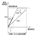
- FIG. 3B is a graph showing the relationship between the accumulated charge amount and accumulation time of the photoelectric conversion unit.
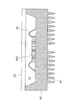
- FIG. 4 is an example of a schematic cross-sectional view of a unit pixel included in the solid-state imaging device according to Embodiment 1 of the present invention.
- FIG. 1 is a functional block diagram showing the configuration of the imaging apparatus according to Embodiment 1 of the present invention.
- FIG. 2 is a circuit configuration diagram of a pixel block included in the solid-state imaging device according to Embodiment 1 of the present invention.
- FIG. 3A is an operation flowchart of the signal processing apparatus according to Embod
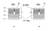
- FIG. 5 is a cross-sectional view of the structure of the optical attenuating filter according to Embodiment 1 of the present invention and a diagram illustrating the driving principle.
- FIG. 6 is a diagram showing a light transmission spectrum of WO 3 before and after hydrogen introduction.
- FIG. 7 is an example of a structural cross-sectional view of a solid-state imaging device showing a modification according to Embodiment 1 of the present invention.
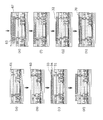
- FIG. 8 is a process cross-sectional view of the optical attenuation filter included in the solid-state imaging device according to Embodiment 1 of the present invention.
- FIG. 9 is a schematic cross-sectional view illustrating a mounted state of the solid-state imaging device according to Embodiment 1 of the present invention.
- FIG. 10 is a schematic diagram of an imaging region of the solid-state imaging device according to Embodiment 2 of the present invention.
- FIG. 11A is an operation flowchart of the signal processing apparatus according to Embodiment 2 of the present invention.
- FIG. 11B is a graph showing the adjustment operation of the accumulated charge amount of the photoelectric conversion unit by the signal processing device.
- FIG. 12 is a schematic diagram of an imaging region of the solid-state imaging device according to Embodiment 3 of the present invention.
- FIG. 13 is a structural sectional view of the optical attenuation filter 36 according to the fourth embodiment of the present invention and a diagram showing the driving principle.
- FIG. 14 is a sectional view of the structure of a conventional solid-state imaging device described in Patent Document 1.
- FIG. 1 is a functional block diagram showing the configuration of the imaging apparatus according to Embodiment 1 of the present invention.
- An imaging device 200 illustrated in the figure is a digital camera including a solid-state imaging device 100, a lens 201, a drive circuit 202, a signal processing device 203, and an external interface unit 204.
- the signal processing device 203 drives the solid-state imaging device 100 through the driving circuit 202, takes in an output signal from the solid-state imaging device 100, and outputs the internally processed signal to the outside via the external interface unit 204.
- the solid-state imaging device 100 has an active light attenuation filter for attenuating the amount of incident light in units of pixel units or pixel blocks, and the signal processing device 203 sets the attenuation rate of the light attenuation filter in units of pixels or pixels in advance. By setting in block units, it is possible to adjust the amount of light incident on the imaging region.
- FIG. 2 is a circuit configuration diagram of a pixel block included in the solid-state imaging device according to Embodiment 1 of the present invention.
- the solid-state imaging device 100 shown in the figure includes an imaging region 2 in which unit pixels 1 each having a photoelectric conversion unit 11 that is a photodiode are two-dimensionally arranged, a horizontal shift register 3 for selecting a pixel signal, and A vertical shift register 4 and an output terminal 5 for providing a signal from the selected unit pixel 1 to the outside are provided.
- the imaging area 2 includes a plurality of unit pixels 1.
- the unit pixel 1 includes a photoelectric conversion unit 11, a transfer transistor 12, a reset transistor 13, an amplification transistor 14, and a selection transistor 15.
- Each of the transfer transistor 12, the reset transistor 13, the amplification transistor 14, and the selection transistor 15 is configured by a MOS transistor.
- the solid-state imaging device 100 includes a light attenuation filter 16 and a selection transistor 17.
- the light attenuation filter 16 is formed on the incident light side of the imaging region 2.
- the selection transistor 17 is disposed between the voltage line 18 and the light attenuation filter 16.
- the gate of the selection transistor 17 is connected to the readout line 19 and switches between conduction and non-conduction between the voltage line 18 and the light attenuation filter 16 according to a control signal from the readout line 19.
- Both the positive potential and the negative potential can be selectively applied to the voltage line 18.
- a positive voltage is applied to the voltage attenuation line 16 by applying a positive voltage to the voltage line 18 and turning on the selection transistor 17.
- the conduction period of the selection transistor 17 that is, the period during which the positive voltage is applied to the light attenuation filter 16
- a desired transmittance of the light attenuation filter 16 can be obtained.
- the selection transistor 17 is turned off, and normal imaging driving is performed with the set transmittance.
- a negative voltage is applied to the voltage line 18 to turn on the selection transistor 17 and return the light attenuation filter 16 to its original state.
- the transmittance adjustment operation of the light attenuation filter 16 and the reset operation of the photoelectric conversion unit 11 are sequentially performed in time series with the imaging operation of the unit pixel 1, the photoelectric conversion unit before luminance signal saturation measurement and imaging operation described later is performed. It is possible to reset the charge accumulated in 11.
- the transmittance adjustment operation of the light attenuation filter 16, the imaging operation and the reset operation of the unit pixel 1 can be individually operated without installing a new signal line.
- the selection transistor 17 for controlling the voltage application to the optical attenuation filter 16 is provided.
- the selection transistor 17 can be made unnecessary by driving the voltage line 18 in a pulsed manner. is there.
- the readout line 19 may be turned off, and if the voltage line 18 is set to 0 V during the exposure period, the transmittance set by the transmittance adjustment operation. Does not change during exposure.
- a voltage is applied to the voltage line 18, but even if the transmittance of the light attenuation filter 16 changes at that time, it becomes a pseudo signal if charge has already been accumulated.
- the readout line 19 may be turned off again and the light attenuation filter 16 may be turned off after readout.
- a transistor for controlling voltage application to the light attenuation filter 16 is not necessary, and therefore the light attenuation filter 16 can be mounted on each pixel even for a fine pixel.
- the signal processing device 203 determines whether or not the luminance signal output from the pixel block including the unit pixel 1 or the plurality of unit pixels 1 is saturated before the imaging exposure, and the determination unit determines the luminance signal. Is determined to be saturated, the transmittance of the light attenuating filter 16 is set by setting the voltage applied to the light attenuating filter 16 before the image capturing exposure so that the luminance signal at the time of image capturing exposure is less than the saturation signal.
- a transmittance control unit that is electrically controlled.
- FIG. 3A is an operation flowchart of the signal processing apparatus according to Embodiment 1 of the present invention.
- FIG. 3B is a graph showing the relationship between the accumulated charge amount and the accumulation time of the photoelectric conversion unit.
- step S01 luminance signal saturation measurement is performed by the signal processing device 203 (step S01), and after the transmittance of the light attenuation filter 16 is decreased (step S02), the subject is imaged (step S03). That's it.
- the determination unit of the signal processing device 203 calculates ⁇ Q / t1 corresponding to the inclination of the graph shown in FIG. 3B from the accumulated charge amount ⁇ Q accumulated by the exposure in the period t1 as the luminance signal saturation measurement.
- the luminance signal in the exposure period required when the incident light is not attenuated by the light attenuation filter 16 is saturated, that is, whether the accumulated charge amount in the period reaches the saturated charge amount. judge.
- the signal processing device 203 sets a threshold for the luminance signal intensity in advance in the signal processing area.
- the transmittance control unit operates the light attenuation filter 16 to reduce ⁇ Q / t1 corresponding to the storage efficiency by the transmittance T to prevent saturation.
- the photoelectric conversion unit 11 determines whether the photoelectric conversion unit 11 has saturation illuminance or saturation luminance for shooting under high illuminance or a high brightness subject, and the light of the light attenuation filter 16 is not saturated. Transmittance can be controlled. Therefore, imaging under high illuminance is possible.
- the light transmission amount at the time of imaging exposure is controlled by the light attenuation filter 16 by the luminance signal saturation determination performed in advance by preliminary imaging, downsizing can be realized and imaging can be performed even under high illuminance. It becomes possible to provide an imaging device 200 that can be used.
- FIG. 4 is an example of a schematic cross-sectional view of a unit pixel included in the solid-state imaging device according to Embodiment 1 of the present invention.
- the unit pixel 1 shown in the figure includes a photoelectric conversion unit 11, a light attenuation filter 16, a semiconductor substrate 20, a gate and gate wiring 22, an interlayer film 24, a color filter 26, and a planarization film 27. , Microlenses 28 and wiring layers 57 and 59.
- the light attenuation filter 16 is disposed above the uppermost wiring layer 59 and below the color filter 26.
- the wiring material of the wiring layers 57 and 59 is, for example, AlCu. Also, the number of wiring layers is two layers of wiring layers 57 and 59.
- the light attenuation filter 16 includes transparent electrodes 31 and 32, an active material layer 33, and a solid electrolyte layer 34, and a laminated film of the active material layer 33 and the solid electrolyte layer 34 is sandwiched between the transparent electrodes 31 and 32. It has a capacitor structure.
- the transparent electrodes 31 and 32 are each electrically connected to the wiring layer 59, and the lower transparent electrode electrically connected to the selection transistor 17 (not shown) formed on the semiconductor substrate via the wiring layer 59. And the upper transparent electrode. As described above, the applied voltage of the light attenuation filter 16 is controlled by the conduction and non-conduction of the selection transistor 17.
- FIG. 5 is a structural sectional view of the optical attenuating filter according to the first embodiment of the present invention and a diagram showing a driving principle.
- the light attenuation filter 16 in the present embodiment uses an electrochromic element.
- An electrochromic element is a generic term for elements in which the absorption spectrum of a material changes when a voltage is applied, and the color changes.
- an element whose transmittance is changed by changing the orientation of liquid crystal molecules by an electric field, such as liquid crystal is one of the electrochromic elements.
- electrochromic devices using solid electrolytes that change the absorption spectrum due to redox reactions caused by ion migration in solids have no polarization dependence like liquid crystals, and there are also materials that exhibit unique spectra. Therefore, it is widely used for display elements.
- the state A shown in FIG. 5A indicates that the active material of the active material layer 33 is in an oxidized state by applying a positive voltage to the transparent electrode 32 on the active material layer 33 side. Show. Thereby, ions move from the active material layer 33 to the solid electrolyte layer 34, and at the same time, electrons are emitted from the active material layer 33 to the transparent electrode 32. In this state A, the light attenuation filter 16 is in a transparent state.
- the conduction ion is basically a cation
- the cation moves in the direction opposite to the direction of the electrons.
- a current corresponding to an oxidation-reduction current corresponding to the amount of ion movement from the active material enters and exits.
- the amount of movement of ions can be controlled by the voltage application time to the electrodes, whereby the amount of transmitted light can be controlled, and a solid-state imaging device capable of imaging even under high illuminance can be realized.
- the active material layer 33 constituting the light attenuation filter 16 is made of any one material of amorphous oxides represented by WO 3 , MoO 3 , and IrO 2 .
- the solid electrolyte layer 34 is made of at least one of oxide materials represented by ZrO 2 , Ta 2 O 5 , Cr 2 O 3 , V 2 O 5 , SiO 2 , Nb 2 O 5 , and HfO 2 .
- WO 3 is used as a constituent material of the active material layer 33 and Ta 2 O 5 is used as a constituent material of the solid electrolyte layer 34
- the combination of WO 3 and Ta 2 O 5 is one of the common combinations for electrochromic devices.
- an oxidation-reduction reaction accompanied by ion transfer occurs between WO 3 and Ta 2 O 5, and the electronic structure of WO 3 changes greatly. It is possible to control in steps between the transparent state and the colored state.
- WO 3 is a highly ionic oxide, and W in WO 3 exists in a state close to W 6+ in which valence electrons have been taken away by O. In this state, it is a transparent material having a band gap of about 3.8 eV. However, if hydrogen or an alkali metal is present here, they enter between W and O and give their own electrons to the W side. Causes a reduction reaction. This reduced electron occupies the d electron level of W and greatly contributes to light absorption.
- FIG. 6 is a diagram showing a light transmission spectrum of WO 3 before and after hydrogen introduction.
- HxWO 3 is a state in which hydrogen is introduced into WO 3 at a non-stoichiometric ratio. As shown in the figure, in the state without hydrogen (WO 3 ), it can be seen that the visible light region has a very high transparency.
- H x WO 3 into which hydrogen is introduced strong light absorption is observed from green to red. Even in the blue region where the light absorption is relatively small, the transmittance is reduced by about 40%, and since blue is originally a color with low visibility, it becomes a sufficient light attenuation filter for visible light.
- the active material layer 33 is preferably an amorphous film.
- WO 3 is a crystal
- the number of sites where ions such as hydrogen enter is reduced, and at the same time, the ion movement speed is reduced.
- an amorphous film is optimal for the present invention.
- amorphous WO 3 can be formed at a low temperature, it has a very high affinity with the silicon process.
- the solid electrolyte layer 34 uses a H + ion as a conductive ion, for loading and unloading the H + ions between the active material layer 33, a transparent material is moved in the storage and H + ions of H + ions is easy Desired. Further, since the conductive ions are driven by the electric field in the solid electrolyte layer 34 and the active material layer 33, the solid electrolyte layer 34 is required to have insulating properties. ZrO 2 , Ta 2 O 5 , Cr 2 O 3 , V 2 O 5 , SiO 2 , Nb 2 O 5 and HfO 2 are transparent oxide dielectrics with excellent insulating properties and contain H + ions.
- the present embodiment is the best mode for conducting H + ions.
- the device structure according to the first exemplary embodiment of the present invention includes an electrochromic element including a pair of active material layers 33 and a solid electrolyte layer 34 provided above the uppermost wiring layer 59 with an interlayer film therebetween. Therefore, a process for forming a light attenuating filter is required before forming a color filter. Details of the manufacturing process after the uppermost wiring layer will be described below.
- FIG. 7 is an example of a cross-sectional view of the structure of the solid-state imaging device showing a modification according to Embodiment 1 of the present invention.
- the solid-state imaging device 110 shown in the figure is a MOS image sensor.
- FIG. 8 is a process cross-sectional view of the optical attenuation filter included in the solid-state imaging device according to Embodiment 1 of the present invention.
- a diffusion region 52 is formed in the semiconductor substrate 20 by ion implantation.
- an imaging region 51 and a peripheral circuit region 50 of the pixel portion are formed on the semiconductor substrate 20.
- the transistor 54 is electrically isolated by the element isolation part 53.
- an interlayer film 56 made of an insulator such as BPSG (Boron Phosphorate Silicate Glass) is formed, planarized by CMP (Chemical Mechanical Polishing) or etch back, and then contact holes are formed by dry etching.
- the metal plug 55 is formed by a metal CVD method. With the metal plug 55 exposed, an aluminum film is formed by sputtering or the like, and patterning is performed by dry etching to produce the wiring layer 57. By repeating this process configuration, a multilayer wiring structure can be made.
- the transistor 54 corresponds to, for example, any of the transfer transistor 12, the reset transistor 13, the amplification transistor 14, and the selection transistors 15 and 17 illustrated in FIG.
- the interlayer film 24 made of an insulating dielectric is formed on the upper portion of the first wiring layer 57 to planarize the metal plug. After the formation, a second wiring layer 59 is formed.
- an interlayer film 61 made of an insulating dielectric is formed of BPSG and planarized using CMP.
- a metal plug 60 is formed. Here, the metal plug 60 is exposed.
- the transparent electrode 31, the solid electrolyte layer 34, and the active material layer 33 of the light attenuation filter 16 are stacked.
- the lower transparent electrode 31 is electrically connected to the metal plug 60. Since the light attenuating filter 16 basically needs to transmit light, the transparent electrode 31 uses ITO transparent to visible light.
- the film thickness of the transparent electrode 31 is, for example, 200 nm.
- the light attenuation filter 16 is provided above the two wiring layers 57 and 59.
- the pixel structure is not limited to this, and the light attenuation filter 16 is not limited to the first layer. It may be provided between the wiring layer 57 and the second wiring layer 59.
- patterning for element isolation is performed by dry etching.
- an insulating interlayer film 67 such as BSPG or FSG is deposited and planarized by CMP. Thereafter, via holes for metal plugs are formed by oxide film dry etching. Thereafter, a metal including the metal plug 65 is formed by metal CVD.
- the surface is polished by CMP until the WO 3 of the active material layer 33 is exposed.
- a transparent electrode 32 is formed and patterned. At this time, the metal plug 65 and the transparent electrode 32 are electrically connected. Since the light attenuation filter 16 basically needs to transmit light, the transparent electrode 32 uses ITO transparent to visible light.
- a planarizing film 70 is formed. Thereafter, although not shown, a color filter and a microlens are formed. As described above, the solid-state imaging device 110 of the present invention is formed.
- the light attenuating filter 16 capable of adjusting the transmittance in units of pixels is arranged continuously with the stacking process of the unit pixels 1, so that the pixel composed of the unit pixel 1 or the plurality of unit pixels 1. It is possible to set exposure conditions for each block. Therefore, even if a high-luminance subject and a low-luminance subject are mixed within the angle of view, the amount of light transmission can be limited for each pixel unit or pixel block. A wide dynamic range that is not saturated with respect to the region can be realized.
- the light attenuation filter 16 is integrally formed with the pixel on the photoelectric conversion unit via the interlayer films 24 and 61 made of a dielectric, the light attenuation filter is formed on the pixel after being formed separately from the pixel. Compared with the structure, it is possible to suppress ghost and flare due to multiple reflection.
- the ITO electrodes which are the transparent electrodes 31 and 32 are produced by using, for example, a pulse laser film forming method (PLD method).
- PLD method is a method in which a desired material is focused and irradiated with a pulse laser, and the material surface evaporates instantaneously and locally, causing the material atoms to evaporate and reattach to a substrate at another location. It is a method to form a film.
- a highly uniform oxide film can be formed by using an oxide as a target for atomic evaporation by a laser and using oxygen as a film formation atmosphere.
- an ITO target is irradiated with a KrF laser (wavelength 248 nm) that is an excimer laser to form a film on the wiring.
- the film forming temperature is preferably about 300 ° C. as the temperature at which the wiring layers 57 and 59 made of aluminum are not dissolved.
- the film thickness of the transparent electrodes 31 and 32 is desirably 50 nm or more because resistance increases if it is too thin. On the other hand, if the film thickness is too thick, the distance from the microlens to the photoelectric conversion unit 11 becomes longer than the focal length of the microlens, thereby reducing the light collection degree. In this embodiment, the film thickness of ITO is 200 nm, but it is desirable that the film thickness be as thin as possible.
- a solid electrolyte layer 34 and an active material layer 33 are stacked on the transparent electrode 31.
- the active material layer 33 and the solid electrolyte layer 34 use WO 3 and Ta 2 O 5 , respectively, and the film thicknesses are 300 nm and 200 nm, respectively.
- the WO 3 film and the Ta 2 O 5 film are also formed using the PLD method.
- a Ta 2 O 5 film is formed on the transparent electrode 31 made of ITO in an oxygen atmosphere at a film forming temperature of about 400 ° C.
- the film is formed at a temperature higher than about 400 ° C.
- the aluminum wiring layer may be dissolved.
- the oxide film formation at a low temperature the oxidation does not proceed sufficiently, and a large amount of oxygen vacancies are contained at a low density due to insufficient supply of oxygen, which causes a decrease in insulation and a decrease in transmittance. Therefore, from this point of view, the film formation at the highest possible temperature is desirable, and the film formation is performed at about 400 ° C.
- hydrogen is introduced into Ta 2 O 5 by performing hydrogen annealing at about 400 ° C. for about 1 minute.
- Long-time hydrogen annealing reduces Ta 2 O 5 , which not only leads to an increase in leakage current and a decrease in transparency, but also causes a decrease in the conductivity of the ITO transparent electrode. Therefore, in order to dope low concentration hydrogen into the outermost Ta 2 O 5 film so that excessive hydrogen is not introduced, it is necessary to control the time and flow rate of hydrogen annealing.
- the temperature of about 400 ° C. is required for WO 3 to take in hydrogen atoms, but hydrogen can be introduced by immersing in dilute hydrochloric acid for about 10 to 60 seconds. As described above, the solid electrolyte layer 34 is formed.
- a WO 3 film is formed on Ta 2 O 5 at a film forming temperature of 200 ° C. again by the PLD method.
- the temperature of the WO 3 film is preferably lower than about 300 ° C.
- the WO 3 film is formed at about 200 ° C. Yes.
- the active material layer 33 according to the present invention is preferably an amorphous film. In the case of WO 3 in the case of a crystal, the number of sites where ions such as hydrogen enter decreases, and at the same time, the ion movement speed becomes slow.
- amorphous since amorphous has a large number of sites where ions enter and its ion conduction speed is faster than that of crystals, it can be said to be optimal for the present invention. Furthermore, since amorphous WO 3 can be formed at a low temperature, it has a very high affinity with the silicon process. As described above, the active material layer 33 is formed.
- the light attenuation filter 16 can be made thin by the configuration of the light attenuation filter 16 described above, a small solid-state imaging device capable of obtaining a high-definition image can be realized.
- WO 3 and Ta 2 O 5 are used for the active material layer 33 and the solid electrolyte layer 34, respectively.
- the present invention is not limited to this, and a material whose transmission spectrum is changed by ion migration is used.
- the active material layer 33 may be MoO 3 or IrO 2 .
- the solid electrolyte layer 34 may be a transparent insulator containing hydrogen and capable of ionic conduction.
- ZrO 2 , Ta 2 O 5 , Cr 2 O 3 , V 2 O 5 , SiO 2 , Nb 2 O 5 HfO 2 or the like may be used.
- ZrO 2 , Cr 2 O 3, V 2 O 5 and the like are effective materials because of their excellent ion conductivity.
- the active material layer 33 is stacked on the solid electrolyte layer 34.
- a structure in which the solid electrolyte layer 34 is stacked on the active material layer 33 may be used.
- the thickness of the active material layer 33 is about 200 nm, and the thickness of the solid electrolyte layer 34 is about 300 nm.
- the thicknesses of the active material layer 33 are light transmittance, driving speed, and reproducibility. This is a very important parameter from the viewpoint. If the film thickness is too thin, light is transmitted even if it is colored, and the light cannot be sufficiently attenuated.
- the film thickness of the entire layer structure of the device is increased, so that the entire film thickness becomes larger than the focal length of the microlens, and the condensing on the photoelectric conversion unit 11 is reduced. Furthermore, since ions such as hydrogen penetrate deep into the active material, it takes a long time to release all ions by the reverse voltage and to make the active material transparent. This means a reduction in operating speed. In addition, due to repeated operations, hydrogen gradually remains on the active material layer 33 side, and the reproducibility of transmittance modulation is gradually lost. Therefore, efficient exchange of high-concentration hydrogen (such as conductive ions) in the vicinity of the interface between the active material layer 33 and the solid electrolyte layer 34 is important for operating speed, reproducibility, and modulation of transmittance.
- high-concentration hydrogen such as conductive ions
- the film thickness of the active material layer 33 is desirably 100 nm or more and 1000 nm or less.
- the solid electrolyte layer 34 has a film thickness that can contain sufficient hydrogen to be inserted into the active material layer 33 and can efficiently take in hydrogen from the active material layer 33, the solid electrolyte layer The film thickness of 34 is desirably thicker than the active material layer.
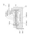
- FIG. 9 is a schematic cross-sectional view illustrating a mounted state of the solid-state imaging device according to Embodiment 1 of the present invention.
- the solid-state imaging device 100 of the present invention is joined to a ceramic pedestal 80 having connection pins 84.
- the metal wire 81 is connected.
- gas 82 is sealed and sealed with a transparent glass plate 83.
- the gas 82 uses a rare gas or N 2 .
- a rare gas is used, Ar is suitable at the lowest cost.
- the solid electrolyte layer 34, the active material layer 33, and the transparent electrodes 31 and 32 included in the solid-state imaging device 100 are all made of an oxide, and excessive hydrogen causes a reduction reaction. Is desirable from the viewpoint of reliability.
- the device structure is provided with a protective film, hydrogen atoms supplied from moisture or the like contained in the atmosphere gradually reduce the oxide and deteriorate the characteristics of the electrochromic device. Therefore, by sealing with a rare gas such as Ar or an inert gas such as N 2 gas, the supply source of hydrogen can be cut off, stable device operation can be realized, and high reliability can be ensured. It becomes possible.
- solid-state imaging device 100 included in the imaging device 200 illustrated in FIG. 1 is preferably incorporated in the imaging device 200 in the mounting state described above.
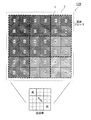
- FIG. 10 is a schematic diagram of an imaging region of the solid-state imaging device according to Embodiment 2 of the present invention.
- the solid-state imaging device 120 shown in the figure is described in Embodiment 1 only in that it has a light attenuation filter 16 for each pixel block composed of a plurality of unit pixels 1 in 2 rows and 2 columns.
- Different from the solid-state imaging devices 100 and 110 Hereinafter, description of the same points as the solid-state imaging devices 100 and 110 will be omitted, and only different points will be described.
- the plurality of unit pixels 1 in the imaging region 2 shown in FIG. 10 are arranged in a Bayer array.
- An independent light attenuation filter 16 is provided for each pixel block that is one unit of the Bayer array, and the light attenuation filter 16 is driven for each Bayer array.
- FIG. 10 shows a state in which the light attenuation filter 16 of the upper left pixel block is set to 100% transmittance, and the lower the pixel block at the lower right, the higher the attenuation factor is set.
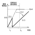
- FIG. 11A is an operation flowchart of the signal processing apparatus according to Embodiment 2 of the present invention.
- FIG. 11B is a graph showing the adjustment operation of the accumulated charge amount of the photoelectric conversion unit by the signal processing device.
- the exposure time is set so that the accumulated charge is not saturated and the gradation of the low-luminance subject can be expressed in the imaging exposure (step S13) shown in FIG. 11A. Is done.
- the signal processing apparatus includes a specifying unit that specifies a region that outputs a saturation signal from a luminance signal intensity distribution of an imaging region acquired in advance by preliminary imaging, and a region that outputs a saturation signal specified by the specifying unit.
- the light attenuating filter 16 is set by setting an applied voltage to the light attenuating filter 16 disposed in the pixel block before the image capturing exposure so that the luminance signal at the time of the image capturing exposure of the included pixel block is equal to or lower than the saturation signal.
- a transmittance control unit for electrically controlling the transmittance of the light.
- the specifying unit performs luminance signal saturation measurement in the exposure period t1 for each pixel block (step S11).
- the transmittance control unit determines that the output from the pixels in the same pixel block is (T / 100) ⁇ ( ⁇ Q / t1) ⁇ t2 ⁇ Q sat (Formula 1)
- T (%) is set for each pixel block so as to satisfy (Step S12).
- Q sat is the saturation charge amount.
- the signal processing apparatus performs imaging exposure on all the pixel blocks using the attenuation rate T set for each pixel block in step S12 (step S13).
- the light attenuation filter 16 is disposed for each pixel block, saturation determination is performed for each pixel block, and exposure conditions are set for each pixel block. A wide dynamic range that is not saturated with respect to a high-luminance pixel region can be realized.
- FIG. 12 is a schematic diagram of an imaging region of the solid-state imaging device according to Embodiment 3 of the present invention.
- the solid-state imaging device 130 shown in the figure has the light attenuation filter 16 only in the R1 pixel and the R2 pixel in the pixel block of the Bayer array composed of the plurality of unit pixels 1 in 2 rows and 2 columns. Only the points differ from the solid-state imaging device 120 described in the second embodiment. Hereinafter, description of the same points as the solid-state imaging device 120 is omitted, and only different points will be described.
- the light attenuation filter 16 is disposed only above the G1 and G2 pixels having the highest visibility in the pixel block that is one unit of the Bayer array.
- the determination unit included in the signal processing device determines in advance whether or not the luminance signals output from the G1 pixel and the G2 pixel are saturated before imaging exposure, and the transmittance control unit included in the signal processing device is determined by the determination unit.
- the applied voltage to the light attenuation filter 16 is set before the image capturing exposure so that the luminance signal at the time of image capturing exposure is equal to or lower than the saturation signal.
- the rate is electrically controlled.
- the light amount adjustment of the G pixel is effective for suppressing the saturation of the luminance signal. As a result, it is possible to realize a wide dynamic range without reducing the S / N of the B signal and R signal with a small signal amount. Further, since the electrochromic driving area is only the area of the green pixel, the driving power can be reduced, and thus a wide dynamic range can be realized with low power consumption.
- FIG. 13 is a structural sectional view of the optical attenuation filter 36 according to the fourth embodiment of the present invention and a diagram showing the driving principle.
- the light attenuation filter 36 described in FIG. 13 is described in FIG. 5 according to the first embodiment only in that the insulating layer 35 is inserted between the solid electrolyte layer 34 and the active material layer 33. Different from the optical attenuation filter 16.
- description of the same points as the light attenuation filter 16 will be omitted, and only different points will be described.
- the light attenuation filter 36 is an electrochromic element using a solid electrolyte, and thus basically requires a pair of transparent electrodes, a solid electrolyte as an insulator, and an active material in which an oxidation-reduction reaction is performed. It is. Moreover, since the electron movement of the active material layer 33 is accompanied by the ion movement, the solid electrolyte layer 34 must be an insulator. This is because the electronic structure of the active material layer 33 is changed due to the reduction reaction and becomes conductive. Therefore, if there is a leakage current on the solid electrolyte layer 34 side, it becomes a capacitor structure, but it becomes a simple resistance and redox. This is because no reaction can occur.
- transition metal oxides such as Ta 2 O 5 and V 2 O 5, which are typical constituent elements of the solid electrolyte layer 34, tend to cause oxygen vacancies as leak sources, and the larger the device area, the more these elements. Leakage causes power loss and makes it impossible to cause sufficient ion movement. In addition, there is a problem with reliability that defects increase due to Joule heat caused by leakage current and leakage increases. Therefore, in order to ensure the insulation of the capacitor structure, it is preferable to insert a thin film insulating layer that is insulative and allows only ions to pass between the solid electrolyte layer 34 and the active material layer 33.
- the insulating layer 35 As a material of the insulating layer 35 which is the thin film insulating layer, SiO 2 , SiON, or SiN is preferable.
- SiO 2 is used as the material of the insulating layer 35, for example, the film thickness is about 5 nm.
- the film forming method is preferably plasma CVD, but may be a reactive sputtering method or a PLD method.
- SiO 2 has excellent insulating properties and is suitable for ion migration of hydrogen, Li and the like.
- the thickness should be as thin as possible, and preferably about 1 to 10 nm.
- the above configuration of the light attenuation filter 36 makes it possible to maintain insulation even when a leak source is present in the solid electrolyte layer 34 made of a transition metal oxide. Therefore, the variation in the transmittance within the surface of the light attenuation filter 36 is suppressed, the reproducibility of the transmittance is ensured, and the transmittance can be maintained for a long time. Therefore, it is possible to provide a solid-state imaging device equipped with a high-performance optical attenuation filter with a high yield.
- Embodiment 5 a solid-state imaging device in which the material configuration of the solid electrolyte layer is different will be described.
- the solid-state imaging device according to the present embodiment is different from the solid-state imaging devices 100 and 110 according to the first embodiment only in the material configuration of the solid electrolyte layer included in the light attenuation filter.
- description of the same points as the light attenuation filter 16 will be omitted, and only different points will be described.
- the solid-state imaging device 140 includes a light attenuation filter 46.
- the light attenuation filter 46 includes a transparent electrode 31, a solid electrolyte layer 47, an active material layer 33, and a transparent electrode 32 in the order of lamination.
- the solid electrolyte layer 47 is made of one of oxides of zirconia, tantalum, chromium, vanadium, niobium, and hafnium containing any one of Li, Na, and Ag.
- An example of the material of the solid electrolyte layer 47 is LiV 2 O 5 .
- the ion conduction medium of the light attenuating filter 46 according to the present embodiment is hydrogen ions, it is not necessarily hydrogen from the viewpoint of device reliability.
- the principle of changing the transmittance of the active material layer 33 is that electrons are injected at the same time as ions are inserted into the active material layer 33 and a reduction reaction occurs in which the valence of the central metal ion is reduced.
- the ion to be inserted may be anything as long as it can move in the solid. However, since it is an element that diffuses in a solid and has excellent controllability, hydrogen having the smallest atomic radius and ion radius is most suitable. However, on the other hand, in device operation, hydrogen is not necessarily optimal due to the influence of the operating environment on the reliability and the process yield. For example, degassing due to high temperature operation may occur.
- Li + is used as ions.
- Li along with H, has a small ionic radius and a very small ionization potential, and thus easily causes a redox reaction.
- hydrogen annealing or acid immersion has been described as a method for introducing hydrogen.
- Li can be handled as a solid material source of the film forming apparatus, so that quantitative introduction of Li is possible.
- the amount of Li introduced may be an indefinite ratio as the chemical composition, but since it is used as a solid material source of the film forming apparatus, in this embodiment, what is expressed as LiV 2 O 5 as a chemical formula is used.
- Li is used as an ionic element.
- an alkali metal that easily causes redox may be used as long as the ionization potential is low.
- the ion radius must be small, and Li or Na is suitable.
- the valence is preferably 1, and for example, AgV 2 O 5 containing Ag may be used.
- zirconia, tantalum, chromium, vanadium, niobium or hafnium oxides are suitable as solid electrolyte materials that contain Li or Ag and can exist stably.
- metal ions as the ion conduction medium, it is possible to form a solid electrolyte whose composition is quantitatively controlled, and it is possible to manufacture a light attenuation filter having high uniformity. Therefore, the transmittance of the light attenuation filter can be controlled more accurately, and a solid-state imaging device with high yield and high reliability can be provided.
- the solid-state imaging device and imaging device of the present invention can provide a high-performance, high-performance camera having a wide dynamic range, a small size, and a light amount adjustment function. it can.
- the amount of light reaching the pixel block in the luminance saturation region can be attenuated by the light attenuation filter. Therefore, even if the saturation charge amount is reduced by pixel miniaturization, a wide dynamic range can be realized, and the light quantity can be adjusted under high illuminance without a mechanical diaphragm mechanism. Therefore, it is possible to provide a solid-state imaging device capable of obtaining a high-definition image having a small dynamic imaging range and a wide dynamic range.
- the solid-state imaging device and the imaging device of the present invention have been described based on the embodiments, the solid-state imaging device and the imaging device according to the present invention are not limited to the above-described embodiments.
- CMOS type solid-state imaging device has been described as an example.
- the present invention is not limited to this, and a CCD-type solid-state imaging device can achieve the same effect.
- the present invention is particularly useful for a digital camera, and is optimal for use in a solid-state imaging device and camera that require a wide dynamic range and high-quality images.
Landscapes
- Engineering & Computer Science (AREA)
- Multimedia (AREA)
- Signal Processing (AREA)
- Physics & Mathematics (AREA)
- Spectroscopy & Molecular Physics (AREA)
- Solid State Image Pick-Up Elements (AREA)
- Chemical & Material Sciences (AREA)
- Inorganic Chemistry (AREA)
- Transforming Light Signals Into Electric Signals (AREA)
- Blocking Light For Cameras (AREA)
Abstract
La présente invention concerne un dispositif d'imagerie à semi-conducteurs, selon lequel la quantité de lumière peut être réglée, même sans mécanisme d'ouverture, et qui peut effectuer une imagerie sur une large plage dynamique, même sous un haut degré d'éclairage. Le dispositif d'imagerie à semi-conducteurs possède une zone d'imagerie dans laquelle une pluralité d'unités de pixels unitaires (1), chacun étant pourvu d'une unité de conversion photoélectrique (11) qui est formée sur la surface d'un substrat à semi-conducteurs (20), sont disposées en deux dimensions. Le dispositif d'imagerie à semi-conducteurs est muni de couches intermédiaires (24) qui comprennent un corps diélectrique formé sur l'unité de conversion photoélectrique (11) ; de filtres d'atténuation de la lumière (16), qui sont formés sur les couches intermédiaires (24) en unités d'éléments de pixels ou unités de blocs de pixels comprenant une pluralité d'éléments de pixel, et pour lesquels la transmissivité de la lumière est modifiée par l'application sur eux d'une tension ; et de la commutation des transistors qui sont formés de manière à correspondre aux filtres d'atténuation de lumière (16) dans le substrat à semi-conducteurs (20) et qui sécurisent ou bloquent la voie à l'application d'une tension sur les filtres d'atténuation de la lumière (16).
Priority Applications (2)
| Application Number | Priority Date | Filing Date | Title |
|---|---|---|---|
| CN2011800346292A CN103004181A (zh) | 2010-08-04 | 2011-07-15 | 固体摄像装置、摄像装置 |
| US13/749,192 US20130135505A1 (en) | 2010-08-04 | 2013-01-24 | Solid-state imaging device and imaging apparatus |
Applications Claiming Priority (2)
| Application Number | Priority Date | Filing Date | Title |
|---|---|---|---|
| JP2010175664A JP2012039261A (ja) | 2010-08-04 | 2010-08-04 | 固体撮像装置、撮像装置 |
| JP2010-175664 | 2010-08-04 |
Related Child Applications (1)
| Application Number | Title | Priority Date | Filing Date |
|---|---|---|---|
| US13/749,192 Continuation US20130135505A1 (en) | 2010-08-04 | 2013-01-24 | Solid-state imaging device and imaging apparatus |
Publications (1)
| Publication Number | Publication Date |
|---|---|
| WO2012017607A1 true WO2012017607A1 (fr) | 2012-02-09 |
Family
ID=45559133
Family Applications (1)
| Application Number | Title | Priority Date | Filing Date |
|---|---|---|---|
| PCT/JP2011/004045 Ceased WO2012017607A1 (fr) | 2010-08-04 | 2011-07-15 | Dispositif d'imagerie à semi-conducteurs, dispositif d'imagerie |
Country Status (4)
| Country | Link |
|---|---|
| US (1) | US20130135505A1 (fr) |
| JP (1) | JP2012039261A (fr) |
| CN (1) | CN103004181A (fr) |
| WO (1) | WO2012017607A1 (fr) |
Cited By (2)
| Publication number | Priority date | Publication date | Assignee | Title |
|---|---|---|---|---|
| CN103491319A (zh) * | 2012-06-11 | 2014-01-01 | 索尼公司 | 成像装置 |
| CN104065894A (zh) * | 2013-03-19 | 2014-09-24 | 索尼公司 | 固态成像装置,固态成像装置的驱动方法以及电子设备 |
Families Citing this family (12)
| Publication number | Priority date | Publication date | Assignee | Title |
|---|---|---|---|---|
| JP6234024B2 (ja) * | 2012-11-21 | 2017-11-22 | オリンパス株式会社 | 撮像素子、及び撮像装置 |
| JP6504753B2 (ja) * | 2013-06-07 | 2019-04-24 | キヤノン株式会社 | エレクトロクロミック素子、その駆動方法、光学フィルタ、撮像装置、レンズユニットおよび窓材 |
| CN103442185B (zh) * | 2013-09-02 | 2018-06-22 | 上海集成电路研发中心有限公司 | 一种cmos图像像素阵列 |
| JP6700051B2 (ja) * | 2016-01-26 | 2020-05-27 | 日本放送協会 | 撮像素子および撮像装置 |
| CN109489833A (zh) * | 2018-11-23 | 2019-03-19 | 杭州大立微电子有限公司 | 红外传感器及其形成方法 |
| JP6737325B2 (ja) * | 2018-12-25 | 2020-08-05 | 株式会社リコー | 撮像モジュール及び撮像装置 |
| CN113949818A (zh) * | 2020-07-17 | 2022-01-18 | 深圳市万普拉斯科技有限公司 | 一种像素结构及其的曝光方法 |
| JP2022175162A (ja) * | 2021-05-13 | 2022-11-25 | 凸版印刷株式会社 | 監視カメラ |
| CN113489924A (zh) * | 2021-07-14 | 2021-10-08 | 长春长光奥闰光电科技有限公司 | 成像方法 |
| CN113382176A (zh) * | 2021-07-14 | 2021-09-10 | 长春长光奥闰光电科技有限公司 | 成像系统及成像方法 |
| US11978751B1 (en) * | 2023-01-10 | 2024-05-07 | Taiwan Semiconductor Manufacturing Company, Ltd. | Pixel sensors and methods of forming the same |
| WO2026048514A1 (fr) * | 2024-08-30 | 2026-03-05 | 富士フイルム株式会社 | Dispositif d'imagerie, procédé de commande, et programme de commande |
Citations (3)
| Publication number | Priority date | Publication date | Assignee | Title |
|---|---|---|---|---|
| JPH08294059A (ja) * | 1995-04-21 | 1996-11-05 | Canon Inc | 撮像装置 |
| JPH0946717A (ja) * | 1995-07-28 | 1997-02-14 | Canon Inc | 撮像装置 |
| JP2008124941A (ja) * | 2006-11-14 | 2008-05-29 | Matsushita Electric Ind Co Ltd | 撮像システム、及び可変フィルタの制御方法 |
Family Cites Families (1)
| Publication number | Priority date | Publication date | Assignee | Title |
|---|---|---|---|---|
| JPH09129859A (ja) * | 1995-10-31 | 1997-05-16 | Kyocera Corp | 固体撮像素子 |
-
2010
- 2010-08-04 JP JP2010175664A patent/JP2012039261A/ja active Pending
-
2011
- 2011-07-15 CN CN2011800346292A patent/CN103004181A/zh active Pending
- 2011-07-15 WO PCT/JP2011/004045 patent/WO2012017607A1/fr not_active Ceased
-
2013
- 2013-01-24 US US13/749,192 patent/US20130135505A1/en not_active Abandoned
Patent Citations (3)
| Publication number | Priority date | Publication date | Assignee | Title |
|---|---|---|---|---|
| JPH08294059A (ja) * | 1995-04-21 | 1996-11-05 | Canon Inc | 撮像装置 |
| JPH0946717A (ja) * | 1995-07-28 | 1997-02-14 | Canon Inc | 撮像装置 |
| JP2008124941A (ja) * | 2006-11-14 | 2008-05-29 | Matsushita Electric Ind Co Ltd | 撮像システム、及び可変フィルタの制御方法 |
Cited By (3)
| Publication number | Priority date | Publication date | Assignee | Title |
|---|---|---|---|---|
| CN103491319A (zh) * | 2012-06-11 | 2014-01-01 | 索尼公司 | 成像装置 |
| CN103491319B (zh) * | 2012-06-11 | 2018-03-13 | 索尼半导体解决方案公司 | 成像装置 |
| CN104065894A (zh) * | 2013-03-19 | 2014-09-24 | 索尼公司 | 固态成像装置,固态成像装置的驱动方法以及电子设备 |
Also Published As
| Publication number | Publication date |
|---|---|
| JP2012039261A (ja) | 2012-02-23 |
| CN103004181A (zh) | 2013-03-27 |
| US20130135505A1 (en) | 2013-05-30 |
Similar Documents
| Publication | Publication Date | Title |
|---|---|---|
| WO2012017607A1 (fr) | Dispositif d'imagerie à semi-conducteurs, dispositif d'imagerie | |
| JP2012084814A (ja) | 固体撮像装置、半導体装置及びカメラ | |
| US11665436B2 (en) | Imaging device and camera system | |
| US10910424B2 (en) | Solid-state image pickup unit, method of manufacturing the same, and electronic apparatus | |
| JP6099420B2 (ja) | 発光装置 | |
| JP5942901B2 (ja) | 固体撮像素子および電子機器 | |
| US9167234B2 (en) | Display device | |
| CN108735767A (zh) | 摄像装置和电子设备 | |
| JP2020161831A (ja) | 半導体装置 | |
| JP2004205628A (ja) | エレクトロクロミック素子 | |
| TW200952179A (en) | Thin film transistor and display | |
| KR20120112016A (ko) | 고체 촬상 소자 및 전자기기 | |
| WO2016158074A1 (fr) | Dispositif d'affichage, procédé de production de dispositif d'affichage et équipement électronique | |
| KR20140129347A (ko) | 유기 발광 다이오드형 발광 소자의 전극 | |
| CN114616690A (zh) | 有机装置及其制造方法、显示装置、光电转换装置、电子设备、照明装置和移动体 | |
| US11985431B2 (en) | Imaging system with an electronic shutter | |
| JP2022105609A (ja) | レーザ加工装置 | |
| JP2025182128A (ja) | 表示装置、電子機器、及びヘッドマウントディスプレイ | |
| US8618588B2 (en) | Anti-blooming pixel sensor cell with active neutral density filter, methods of manufacture, and design structure | |
| US20100148291A1 (en) | Ultraviolet light filter layer in image sensors | |
| WO2020246133A1 (fr) | Élément d'imagerie et dispositif d'imagerie | |
| CN2643573Y (zh) | 摄像装置 | |
| JP2003084687A (ja) | 半導体装置およびその作製方法 | |
| JP7150416B2 (ja) | 電子機器 | |
| CN112534802B (zh) | 摄像装置的工作方法 |
Legal Events
| Date | Code | Title | Description |
|---|---|---|---|
| 121 | Ep: the epo has been informed by wipo that ep was designated in this application |
Ref document number: 11814247 Country of ref document: EP Kind code of ref document: A1 |
|
| NENP | Non-entry into the national phase |
Ref country code: DE |
|
| 122 | Ep: pct application non-entry in european phase |
Ref document number: 11814247 Country of ref document: EP Kind code of ref document: A1 |