WO2012029263A1 - Procédé de production d'un module de cellule photovoltaïque - Google Patents
Procédé de production d'un module de cellule photovoltaïque Download PDFInfo
- Publication number
- WO2012029263A1 WO2012029263A1 PCT/JP2011/004735 JP2011004735W WO2012029263A1 WO 2012029263 A1 WO2012029263 A1 WO 2012029263A1 JP 2011004735 W JP2011004735 W JP 2011004735W WO 2012029263 A1 WO2012029263 A1 WO 2012029263A1
- Authority
- WO
- WIPO (PCT)
- Prior art keywords
- cell module
- solar cell
- manufacturing
- unevenness
- laminate
- Prior art date
- Legal status (The legal status is an assumption and is not a legal conclusion. Google has not performed a legal analysis and makes no representation as to the accuracy of the status listed.)
- Ceased
Links
Images




Classifications
-
- H—ELECTRICITY
- H10—SEMICONDUCTOR DEVICES; ELECTRIC SOLID-STATE DEVICES NOT OTHERWISE PROVIDED FOR
- H10F—INORGANIC SEMICONDUCTOR DEVICES SENSITIVE TO INFRARED RADIATION, LIGHT, ELECTROMAGNETIC RADIATION OF SHORTER WAVELENGTH OR CORPUSCULAR RADIATION
- H10F19/00—Integrated devices, or assemblies of multiple devices, comprising at least one photovoltaic cell covered by group H10F10/00, e.g. photovoltaic modules
- H10F19/80—Encapsulations or containers for integrated devices, or assemblies of multiple devices, having photovoltaic cells
-
- H—ELECTRICITY
- H10—SEMICONDUCTOR DEVICES; ELECTRIC SOLID-STATE DEVICES NOT OTHERWISE PROVIDED FOR
- H10F—INORGANIC SEMICONDUCTOR DEVICES SENSITIVE TO INFRARED RADIATION, LIGHT, ELECTROMAGNETIC RADIATION OF SHORTER WAVELENGTH OR CORPUSCULAR RADIATION
- H10F71/00—Manufacture or treatment of devices covered by this subclass
-
- Y—GENERAL TAGGING OF NEW TECHNOLOGICAL DEVELOPMENTS; GENERAL TAGGING OF CROSS-SECTIONAL TECHNOLOGIES SPANNING OVER SEVERAL SECTIONS OF THE IPC; TECHNICAL SUBJECTS COVERED BY FORMER USPC CROSS-REFERENCE ART COLLECTIONS [XRACs] AND DIGESTS
- Y02—TECHNOLOGIES OR APPLICATIONS FOR MITIGATION OR ADAPTATION AGAINST CLIMATE CHANGE
- Y02E—REDUCTION OF GREENHOUSE GAS [GHG] EMISSIONS, RELATED TO ENERGY GENERATION, TRANSMISSION OR DISTRIBUTION
- Y02E10/00—Energy generation through renewable energy sources
- Y02E10/50—Photovoltaic [PV] energy
-
- Y—GENERAL TAGGING OF NEW TECHNOLOGICAL DEVELOPMENTS; GENERAL TAGGING OF CROSS-SECTIONAL TECHNOLOGIES SPANNING OVER SEVERAL SECTIONS OF THE IPC; TECHNICAL SUBJECTS COVERED BY FORMER USPC CROSS-REFERENCE ART COLLECTIONS [XRACs] AND DIGESTS
- Y10—TECHNICAL SUBJECTS COVERED BY FORMER USPC
- Y10T—TECHNICAL SUBJECTS COVERED BY FORMER US CLASSIFICATION
- Y10T29/00—Metal working
- Y10T29/53—Means to assemble or disassemble
- Y10T29/5313—Means to assemble electrical device
- Y10T29/5317—Laminated device
Definitions
- the present invention relates to a method for manufacturing a solar cell module having solar cells formed on a flexible substrate.
- the present invention has been made in view of the above circumstances, and an object thereof is to provide a method for manufacturing a solar cell module with improved production efficiency.
- the method for manufacturing a solar cell module according to the present invention includes the following steps. First, a laminated body is formed in which a plurality of solar cells sandwiched between protective films for sealing a laminate and at least one unevenness forming member are stacked. In this laminated body, all the photovoltaic cells are stacked in a state where the protective film located on the light receiving surface side faces the unevenness forming member. Then, by simultaneously laminating the laminated body, a plurality of solar cells are individually sealed with a protective film at the same time.
- the production efficiency of the solar cell module can be improved.
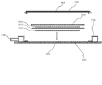
- FIG. 1 is a cross-sectional view for explaining the configuration of a laminating apparatus used in the method for manufacturing a solar cell module according to the first embodiment.
- the solar cell module is manufactured as follows. First, a laminated body of the solar battery cells 202 and the unevenness forming member 300 is disposed on the laminate frame 100.
- the solar battery cell 202 is formed using a flexible substrate. In forming this laminated body, each of the plurality of solar battery cells 202 is disposed on the laminate frame 100 in a state of an intermediate body 200 sandwiched between protective films for sealing the laminate.
- corrugated formation member 300 has opposed all the protective films located in the light-receiving surface side of the photovoltaic cell 202 among protective films.
- the unevenness forming member 300 has unevenness on the surface facing the protective film.
- corrugation formation member 300 is laminated simultaneously,
- the several photovoltaic cell 202 is sealed separately with a protective film simultaneously.
- a frame body 106 is attached on the edge of the laminating frame 100.
- the frame body 106 has an exhaust port 103.
- an upper lid 102 and a diaphragm sheet 104 are detachably attached.
- a closed space is formed by the laminate frame 100, the frame body 106, and the upper lid 102.
- a laminated body of the intermediate body 200 and the unevenness forming member 300 is disposed in the closed space.
- the closed space can be exhausted through the exhaust port 103.
- the laminate frame 100, the frame body 106, the upper lid 102, and the diaphragm sheet 104 are located in the heating furnace 107.
- This laminating apparatus also has an unevenness forming member 300 on the laminating frame 100. And in the laminated body of the intermediate body 200 and the unevenness
- the laminate has two intermediate bodies 200. And in the intermediate body 200 located relatively lower, the photovoltaic cell 202 has the light receiving surface facing downward. Moreover, in the intermediate body 200 positioned relatively upward, the solar cell 202 has the light receiving surface facing upward. A release sheet 310 is located between the two intermediate bodies 200.
- the release sheet 310 is provided to prevent the protective films of the two intermediates 200 from adhering to each other during the lamination process. Concavities and convexities are also formed on the front and back surfaces of the release sheet 310, but the depth of the concavities and convexities may be the same as the concavities and convexities provided on the concavity and convexity forming member 300. Due to the uneven shape of the release sheet 310, an exhaust route is formed between the intermediate body 200 and the release sheet 310 during the lamination process.
- the unevenness forming member 300 is, for example, a wire mesh, a metal sheet in which a plurality of holes are formed can also be used.
- a metal sheet in which a plurality of holes are formed can also be used.
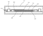
- FIG. 2 is a cross-sectional view showing the configuration of the intermediate body 200.
- the intermediate body 200 is formed by sandwiching the solar battery cell 202 between the protective films 204 and 206.
- the protective film 204 is provided on the light receiving surface side of the solar battery cell 202, and the protective film 206 is provided on the back surface side of the solar battery cell 202.
- the protective film 204 always faces the above-described unevenness forming member 300 when the lamination process is performed, and unevenness is formed on the surface after the lamination process.
- the upper lid 102 and the diaphragm sheet 104 are removed from the frame body 106.
- the intermediate body 200 is arrange
- the release sheet 310 is disposed on the intermediate body 200, and the next intermediate body 200 is disposed on the release sheet 310.
- the intermediate body 200 is arranged so that the protective film 204 faces upward.
- the unevenness forming member 300 is disposed on the intermediate body 200.
- the upper lid 102 and the diaphragm sheet 104 are arranged on the frame body 106.
- the exhaust port 103 is exhausted.
- the closed space between the upper lid 102 and the laminate frame 100 is exhausted.
- an exhaust route is secured between the intermediate body 200 and the release sheet 310 due to the uneven shape of the release sheet 310.
- an exhaust route is secured between the intermediate body 200 and the unevenness forming member 300 by the uneven shape of the unevenness forming member 300. For this reason, it can suppress that air remains partially between the intermediate body 200 and the release sheet 310, and between the intermediate body 200 and the unevenness
- the unevenness of the unevenness forming member 300 is transferred to the protective film 204 on the light receiving surface side of the solar battery cell 202, and the unevenness of the release sheet 310 is formed on the protective film 206 on the back surface side of the solar battery cell 202. Is done.
- the unevenness depth of the release sheet 310 may be approximately the same as the unevenness of the unevenness forming member 300. Due to the unevenness on the incident side of sunlight, reflection of sunlight on the surface of the solar cell module can be suppressed, and sunlight can be effectively taken into the solar cells, and glare caused by reflection of the installed solar cells, etc. The impact on the human environment can be reduced.
- corrugation of a back surface can increase the adhesion area in the adhesion
- the wiring (not shown) for taking out the output of the solar battery cell 202 is drawn out through the protective film 204 or the protective film 206.
- the plurality of solar battery modules 202 can be simultaneously manufactured by simultaneously and individually sealing the plurality of solar battery cells 202 with the protective films 204 and 206. Therefore, the production efficiency of the solar cell module can be increased. Further, in order to increase the power generation efficiency of the solar cell module, it is important to suppress the reflection of light by forming irregularities on the light receiving surface of the solar cell module. Since the concavo-convex forming member 300 is disposed so as to oppose 204, the concavo-convex can be formed on the light receiving surfaces of all the solar cell modules.
- the vertical direction of the light-receiving surface of the plurality of solar cells 202 is staggered. Further, by making the unevenness forming member 300 and the release sheet 310 have different unevenness, the depth and pattern of the unevenness can be changed between the light receiving surface and the back surface of the solar cell module.
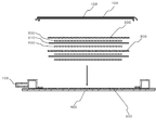
- FIG. 4 is a cross-sectional view showing the method for manufacturing the solar cell module according to the second embodiment, and corresponds to FIG. 3 in the first embodiment.
- the manufacturing method of the solar cell module according to the present embodiment is the same as the manufacturing method of the solar cell module according to the first embodiment except for the following points.
- the laminated body of the intermediate body 200 and the unevenness forming member 300 has a configuration in which at least two second laminated bodies composed of the intermediate body 200, the release sheet 310, and the intermediate body 200 are stacked.
- the two intermediate bodies 200 have the back surfaces of the solar cells 202 facing each other.
- corrugated formation member 300 is arrange
- the unevenness forming member 300 disposed here is, for example, a wire mesh, and similar unevenness is formed on both surfaces. Also in this embodiment, the unevenness forming member 300 is disposed on the uppermost intermediate body 200 and the laminate frame 100, respectively.
- the same effect as that of the first embodiment can be obtained.
- the production efficiency of the solar cell modules can be further increased.
- corrugation in the light-receiving surface and back surface of a solar cell module are below the lower layer and the upper layer of the several photovoltaic cell 202 mutually laminated
- FIG. 5 is a cross-sectional view illustrating a method for manufacturing a solar cell module according to the third embodiment, and corresponds to FIG. 3 in the first embodiment.
- the manufacturing method of the solar cell module according to the present embodiment is the same as the manufacturing method of the solar cell module according to the first embodiment except for the following points.
- the light receiving surfaces of the plurality of intermediate bodies 200 face the same direction. And the intermediate body 200 and the unevenness
- the unevenness forming member 302 is also disposed between the lowermost intermediate body 200 and the laminate frame 100 and on the uppermost intermediate body 200. And each uneven
- each unevenness forming member 302 has the back surface in contact with the light receiving surface of the intermediate body 200 and the surface in contact with the back surface of the intermediate body 200.
- each concave-convex forming member 302 has a back surface in contact with the light receiving surface of the intermediate body 200 and a surface in contact with the back surface of the intermediate body 200.
- the surface of each unevenness forming member 302 is in contact with the light receiving surface of the intermediate body 200 and the back surface is in contact with the back surface of the intermediate body 200.
- the unevenness forming member 302 has the first unevenness formed on the surface facing the light receiving surface of the intermediate 200, and the second unevenness is formed on the surface in contact with the back surface of the intermediate 200. ing.
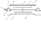
- FIG. 6 is sectional drawing for demonstrating the structure of the laminating apparatus used for the manufacturing method of the solar cell module which concerns on 4th Embodiment.
- the laminating apparatus according to this embodiment has the same configuration as the laminating apparatus according to the first embodiment except for the following points.
- an unevenness forming member 300 is stretched over the entire inner surface of the frame 106.
- the unevenness forming member 300 has similar unevenness on both sides.
- the laminate frame 100 also has a frame shape.
- a second diaphragm sheet 105 is provided so as to seal the hollow portion of the laminate frame 100.
- the second diaphragm sheet 105 is attached to the back surface of the laminate frame 100 using the attachment jig 101.
- FIG. 7 is a diagram for explaining a method of manufacturing a solar cell module using the laminating apparatus shown in FIG.
- the diaphragm sheet 104 and the upper lid 102 are removed from the frame body 106, and the second diaphragm sheet 105 is removed from the laminate frame 100.
- the intermediate body 200 is placed on the concavo-convex forming member 300, and the intermediate body 200 is also arranged on the back side of the concavo-convex forming member 300.
- the diaphragm sheet 104 and the upper lid 102 are disposed on the frame body 106, and the second diaphragm sheet 105 is attached to the laminate frame 100.
- the exhaust port 103 is exhausted.
- FIG. 8 is sectional drawing for demonstrating the manufacturing method of the solar cell module which concerns on 5th Embodiment.
- the manufacturing method of the solar cell module according to the present embodiment is the same as the manufacturing method of the solar cell module according to the first embodiment except for the following points.
- the two intermediate bodies 200 are arranged in directions in which the light receiving surfaces face each other.
- an unevenness forming member 304 is disposed between the two intermediate bodies 200.
- the unevenness forming member 304 has similar unevenness on both sides.
Landscapes
- Photovoltaic Devices (AREA)
- Electroluminescent Light Sources (AREA)
- Engineering & Computer Science (AREA)
- Manufacturing & Machinery (AREA)
Abstract
La présente invention concerne un stratifié, comprenant des cellules photovoltaïques (202) et des éléments formés de façon irrégulière (300), et disposé sur un film stratifié (100). Les cellules photovoltaïques (202) sont formées au moyen de substrats flexibles. Lors de la formation du stratifié, chaque cellule photovoltaïque parmi une pluralité de cellules photovoltaïques (202) est positionnée sur le film stratifié (100) dans un état intermédiaire (200) de prise en sandwich entre le film protecteur pour réaliser l'étanchéité du stratifié. Le film protecteur positionné sur le côté de réception de lumière des cellules photovoltaïques (202) est entièrement tourné vers un élément formé de manière irrégulière (300). Les éléments formés de manière irrégulière (300) présentent une irrégularité sur la surface tournée vers le film protecteur. La stratification du stratifié comprenant les intermédiaires (200) et les éléments formés de façon irrégulière (300) permet d'étanchéifier simultanément la pluralité de cellules photovoltaïques (202) individuellement au moyen du film protecteur.
Priority Applications (2)
| Application Number | Priority Date | Filing Date | Title |
|---|---|---|---|
| US13/820,742 US20130186454A1 (en) | 2010-09-03 | 2011-08-25 | Method of manufacturing photovoltaic module |
| EP11821286.9A EP2613360A1 (fr) | 2010-09-03 | 2011-08-25 | Procédé de production d'un module de cellule photovoltaïque |
Applications Claiming Priority (2)
| Application Number | Priority Date | Filing Date | Title |
|---|---|---|---|
| JP2010-198095 | 2010-09-03 | ||
| JP2010198095A JP2012054515A (ja) | 2010-09-03 | 2010-09-03 | 太陽電池モジュールの製造方法 |
Publications (1)
| Publication Number | Publication Date |
|---|---|
| WO2012029263A1 true WO2012029263A1 (fr) | 2012-03-08 |
Family
ID=45772389
Family Applications (1)
| Application Number | Title | Priority Date | Filing Date |
|---|---|---|---|
| PCT/JP2011/004735 Ceased WO2012029263A1 (fr) | 2010-09-03 | 2011-08-25 | Procédé de production d'un module de cellule photovoltaïque |
Country Status (4)
| Country | Link |
|---|---|
| US (1) | US20130186454A1 (fr) |
| EP (1) | EP2613360A1 (fr) |
| JP (1) | JP2012054515A (fr) |
| WO (1) | WO2012029263A1 (fr) |
Families Citing this family (2)
| Publication number | Priority date | Publication date | Assignee | Title |
|---|---|---|---|---|
| FR3055167B1 (fr) * | 2016-08-16 | 2019-01-25 | Solean | Systeme de lamination, installation incluant un tel systeme de lamination et procede de lamination mis en oeuvre a l'aide d'un tel systeme de lamination |
| KR102478448B1 (ko) * | 2022-08-12 | 2022-12-19 | 주식회사 솔란드 | 유연 태양광 모듈, 이의 텍스처링 방법 및 이의 텍스처링 장치 |
Citations (17)
| Publication number | Priority date | Publication date | Assignee | Title |
|---|---|---|---|---|
| JPS58128846A (ja) * | 1982-01-26 | 1983-08-01 | 東芝ケミカル株式会社 | ポリイミド系樹脂片面銅張積層板の製造方法 |
| JPH0997918A (ja) * | 1995-09-28 | 1997-04-08 | Canon Inc | 太陽電池モジュール |
| JPH10112549A (ja) * | 1996-10-08 | 1998-04-28 | Canon Inc | 太陽電池モジュール |
| JP2948508B2 (ja) | 1995-08-10 | 1999-09-13 | キヤノン株式会社 | 真空ラミネート装置および真空ラミネート方法並びに太陽電池の製造法 |
| JP3176264B2 (ja) | 1995-08-10 | 2001-06-11 | キヤノン株式会社 | 真空ラミネート装置 |
| JP2001252984A (ja) * | 2000-03-13 | 2001-09-18 | Toppan Forms Co Ltd | ラミネート加工方法および加工装置 |
| JP3288876B2 (ja) | 1994-11-04 | 2002-06-04 | キヤノン株式会社 | 太陽電池モジュール及びその製造方法 |
| JP2004297105A (ja) * | 1997-10-30 | 2004-10-21 | Fuji Electric Holdings Co Ltd | 太陽電池モジュールの外部リード接続方法 |
| JP2004311571A (ja) | 2003-04-03 | 2004-11-04 | Fuji Electric Holdings Co Ltd | 太陽電池モジュールの製造方法 |
| JP2007311651A (ja) * | 2006-05-19 | 2007-11-29 | Fuji Electric Systems Co Ltd | 真空ラミネート装置および真空ラミネート方法 |
| JP2008296583A (ja) | 2007-05-30 | 2008-12-11 | Robert Buerkle Gmbh | 板状加工物積層方法及び板状加工物積層装置 |
| WO2009113643A1 (fr) * | 2008-03-12 | 2009-09-17 | 京セラ株式会社 | Module de cellule solaire et son procédé de fabrication |
| JP2010005920A (ja) * | 2008-06-26 | 2010-01-14 | Panasonic Electric Works Co Ltd | 積層品の製造装置及び製造方法 |
| JP2010012786A (ja) | 2008-07-02 | 2010-01-21 | Robert Buerkle Gmbh | 板状加工物積層方法及び板状加工物積層装置 |
| JP2010023485A (ja) | 2008-06-18 | 2010-02-04 | Kyocera Corp | 太陽電池モジュールのラミネータ |
| JP2010149506A (ja) | 2008-11-26 | 2010-07-08 | Kyocera Corp | 太陽電池モジュールのラミネータ及びこれにより製造された太陽電池モジュール |
| JP2010198095A (ja) | 2009-02-23 | 2010-09-09 | Kyocera Corp | 浸水検出装置、浸水検出方法および通信装置 |
Family Cites Families (1)
| Publication number | Priority date | Publication date | Assignee | Title |
|---|---|---|---|---|
| JPH11214724A (ja) * | 1998-01-21 | 1999-08-06 | Canon Inc | 太陽電池モジュール及びその製造方法と施工方法、及び太陽光発電システム |
-
2010
- 2010-09-03 JP JP2010198095A patent/JP2012054515A/ja not_active Withdrawn
-
2011
- 2011-08-25 US US13/820,742 patent/US20130186454A1/en not_active Abandoned
- 2011-08-25 EP EP11821286.9A patent/EP2613360A1/fr not_active Withdrawn
- 2011-08-25 WO PCT/JP2011/004735 patent/WO2012029263A1/fr not_active Ceased
Patent Citations (17)
| Publication number | Priority date | Publication date | Assignee | Title |
|---|---|---|---|---|
| JPS58128846A (ja) * | 1982-01-26 | 1983-08-01 | 東芝ケミカル株式会社 | ポリイミド系樹脂片面銅張積層板の製造方法 |
| JP3288876B2 (ja) | 1994-11-04 | 2002-06-04 | キヤノン株式会社 | 太陽電池モジュール及びその製造方法 |
| JP2948508B2 (ja) | 1995-08-10 | 1999-09-13 | キヤノン株式会社 | 真空ラミネート装置および真空ラミネート方法並びに太陽電池の製造法 |
| JP3176264B2 (ja) | 1995-08-10 | 2001-06-11 | キヤノン株式会社 | 真空ラミネート装置 |
| JPH0997918A (ja) * | 1995-09-28 | 1997-04-08 | Canon Inc | 太陽電池モジュール |
| JPH10112549A (ja) * | 1996-10-08 | 1998-04-28 | Canon Inc | 太陽電池モジュール |
| JP2004297105A (ja) * | 1997-10-30 | 2004-10-21 | Fuji Electric Holdings Co Ltd | 太陽電池モジュールの外部リード接続方法 |
| JP2001252984A (ja) * | 2000-03-13 | 2001-09-18 | Toppan Forms Co Ltd | ラミネート加工方法および加工装置 |
| JP2004311571A (ja) | 2003-04-03 | 2004-11-04 | Fuji Electric Holdings Co Ltd | 太陽電池モジュールの製造方法 |
| JP2007311651A (ja) * | 2006-05-19 | 2007-11-29 | Fuji Electric Systems Co Ltd | 真空ラミネート装置および真空ラミネート方法 |
| JP2008296583A (ja) | 2007-05-30 | 2008-12-11 | Robert Buerkle Gmbh | 板状加工物積層方法及び板状加工物積層装置 |
| WO2009113643A1 (fr) * | 2008-03-12 | 2009-09-17 | 京セラ株式会社 | Module de cellule solaire et son procédé de fabrication |
| JP2010023485A (ja) | 2008-06-18 | 2010-02-04 | Kyocera Corp | 太陽電池モジュールのラミネータ |
| JP2010005920A (ja) * | 2008-06-26 | 2010-01-14 | Panasonic Electric Works Co Ltd | 積層品の製造装置及び製造方法 |
| JP2010012786A (ja) | 2008-07-02 | 2010-01-21 | Robert Buerkle Gmbh | 板状加工物積層方法及び板状加工物積層装置 |
| JP2010149506A (ja) | 2008-11-26 | 2010-07-08 | Kyocera Corp | 太陽電池モジュールのラミネータ及びこれにより製造された太陽電池モジュール |
| JP2010198095A (ja) | 2009-02-23 | 2010-09-09 | Kyocera Corp | 浸水検出装置、浸水検出方法および通信装置 |
Also Published As
| Publication number | Publication date |
|---|---|
| JP2012054515A (ja) | 2012-03-15 |
| US20130186454A1 (en) | 2013-07-25 |
| EP2613360A1 (fr) | 2013-07-10 |
Similar Documents
| Publication | Publication Date | Title |
|---|---|---|
| TW201444104A (zh) | 薄膜太陽能電池板及其製備方法 | |
| JP2010512027A5 (fr) | ||
| JP2016219784A (ja) | 太陽電池モジュール及びその製造方法 | |
| CN110993712B (zh) | 光伏层压件、光伏组件及光伏屋顶 | |
| WO2012029263A1 (fr) | Procédé de production d'un module de cellule photovoltaïque | |
| JP2012064767A (ja) | 太陽電池モジュール | |
| TWI474492B (zh) | 增強光捕捉之太陽光電模組 | |
| CN104960312B (zh) | 柔性光伏组件层压用基板及柔性光伏组件的层压方法 | |
| JP2012079838A (ja) | 太陽電池モジュールとその製造方法 | |
| JP2017022204A (ja) | 太陽電池モジュールの製造方法 | |
| US20130306132A1 (en) | Solar photoelectrical module and fabrication thereof | |
| JP3856224B2 (ja) | 太陽電池モジュールの製造方法 | |
| TW201543704A (zh) | 太陽面板及製造其的方法及包含該太陽面板的壁覆蓋元件 | |
| CN103840022A (zh) | 可弯曲晶体硅太阳能组件 | |
| JP2014132615A (ja) | 太陽電池モジュール | |
| JP2007311651A (ja) | 真空ラミネート装置および真空ラミネート方法 | |
| JP5257927B2 (ja) | 太陽電池パネル | |
| KR102478448B1 (ko) | 유연 태양광 모듈, 이의 텍스처링 방법 및 이의 텍스처링 장치 | |
| JP2013165092A (ja) | 太陽電池モジュールの製造方法 | |
| JP2011198886A (ja) | 太陽電池モジュール及び太陽電池モジュールの製造方法 | |
| JP2013256089A (ja) | 表面保護部材およびその製造方法 | |
| CN223168611U (zh) | 一种压花光伏镀膜玻璃及光伏组件 | |
| CN204725986U (zh) | 柔性光伏组件层压用基板 | |
| JP2016152333A (ja) | 太陽電池モジュール | |
| CN222736527U (zh) | 一种房车船用柔性光伏组件 |
Legal Events
| Date | Code | Title | Description |
|---|---|---|---|
| 121 | Ep: the epo has been informed by wipo that ep was designated in this application |
Ref document number: 11821286 Country of ref document: EP Kind code of ref document: A1 |
|
| NENP | Non-entry into the national phase |
Ref country code: DE |
|
| WWE | Wipo information: entry into national phase |
Ref document number: 2011821286 Country of ref document: EP |
|
| WWE | Wipo information: entry into national phase |
Ref document number: 13820742 Country of ref document: US |