WO2012053782A2 - Procédé de croissance d'un monocristal de carbure de silicium et dispositif afférent - Google Patents
Procédé de croissance d'un monocristal de carbure de silicium et dispositif afférent Download PDFInfo
- Publication number
- WO2012053782A2 WO2012053782A2 PCT/KR2011/007701 KR2011007701W WO2012053782A2 WO 2012053782 A2 WO2012053782 A2 WO 2012053782A2 KR 2011007701 W KR2011007701 W KR 2011007701W WO 2012053782 A2 WO2012053782 A2 WO 2012053782A2
- Authority
- WO
- WIPO (PCT)
- Prior art keywords
- silicon
- silicon carbide
- single crystal
- feedstock
- crucible
- Prior art date
- Legal status (The legal status is an assumption and is not a legal conclusion. Google has not performed a legal analysis and makes no representation as to the accuracy of the status listed.)
- Ceased
Links
Images
Classifications
-
- C—CHEMISTRY; METALLURGY
- C30—CRYSTAL GROWTH
- C30B—SINGLE-CRYSTAL GROWTH; UNIDIRECTIONAL SOLIDIFICATION OF EUTECTIC MATERIAL OR UNIDIRECTIONAL DEMIXING OF EUTECTOID MATERIAL; REFINING BY ZONE-MELTING OF MATERIAL; PRODUCTION OF A HOMOGENEOUS POLYCRYSTALLINE MATERIAL WITH DEFINED STRUCTURE; SINGLE CRYSTALS OR HOMOGENEOUS POLYCRYSTALLINE MATERIAL WITH DEFINED STRUCTURE; AFTER-TREATMENT OF SINGLE CRYSTALS OR A HOMOGENEOUS POLYCRYSTALLINE MATERIAL WITH DEFINED STRUCTURE; APPARATUS THEREFOR
- C30B17/00—Single-crystal growth onto a seed which remains in the melt during growth, e.g. Nacken-Kyropoulos method
-
- C—CHEMISTRY; METALLURGY
- C30—CRYSTAL GROWTH
- C30B—SINGLE-CRYSTAL GROWTH; UNIDIRECTIONAL SOLIDIFICATION OF EUTECTIC MATERIAL OR UNIDIRECTIONAL DEMIXING OF EUTECTOID MATERIAL; REFINING BY ZONE-MELTING OF MATERIAL; PRODUCTION OF A HOMOGENEOUS POLYCRYSTALLINE MATERIAL WITH DEFINED STRUCTURE; SINGLE CRYSTALS OR HOMOGENEOUS POLYCRYSTALLINE MATERIAL WITH DEFINED STRUCTURE; AFTER-TREATMENT OF SINGLE CRYSTALS OR A HOMOGENEOUS POLYCRYSTALLINE MATERIAL WITH DEFINED STRUCTURE; APPARATUS THEREFOR
- C30B15/00—Single-crystal growth by pulling from a melt, e.g. Czochralski method
- C30B15/002—Continuous growth
-
- C—CHEMISTRY; METALLURGY
- C30—CRYSTAL GROWTH
- C30B—SINGLE-CRYSTAL GROWTH; UNIDIRECTIONAL SOLIDIFICATION OF EUTECTIC MATERIAL OR UNIDIRECTIONAL DEMIXING OF EUTECTOID MATERIAL; REFINING BY ZONE-MELTING OF MATERIAL; PRODUCTION OF A HOMOGENEOUS POLYCRYSTALLINE MATERIAL WITH DEFINED STRUCTURE; SINGLE CRYSTALS OR HOMOGENEOUS POLYCRYSTALLINE MATERIAL WITH DEFINED STRUCTURE; AFTER-TREATMENT OF SINGLE CRYSTALS OR A HOMOGENEOUS POLYCRYSTALLINE MATERIAL WITH DEFINED STRUCTURE; APPARATUS THEREFOR
- C30B11/00—Single-crystal growth by normal freezing or freezing under temperature gradient, e.g. Bridgman-Stockbarger method
- C30B11/001—Continuous growth
-
- C—CHEMISTRY; METALLURGY
- C30—CRYSTAL GROWTH
- C30B—SINGLE-CRYSTAL GROWTH; UNIDIRECTIONAL SOLIDIFICATION OF EUTECTIC MATERIAL OR UNIDIRECTIONAL DEMIXING OF EUTECTOID MATERIAL; REFINING BY ZONE-MELTING OF MATERIAL; PRODUCTION OF A HOMOGENEOUS POLYCRYSTALLINE MATERIAL WITH DEFINED STRUCTURE; SINGLE CRYSTALS OR HOMOGENEOUS POLYCRYSTALLINE MATERIAL WITH DEFINED STRUCTURE; AFTER-TREATMENT OF SINGLE CRYSTALS OR A HOMOGENEOUS POLYCRYSTALLINE MATERIAL WITH DEFINED STRUCTURE; APPARATUS THEREFOR
- C30B15/00—Single-crystal growth by pulling from a melt, e.g. Czochralski method
- C30B15/02—Single-crystal growth by pulling from a melt, e.g. Czochralski method adding crystallising materials or reactants forming it in situ to the melt
-
- C—CHEMISTRY; METALLURGY
- C30—CRYSTAL GROWTH
- C30B—SINGLE-CRYSTAL GROWTH; UNIDIRECTIONAL SOLIDIFICATION OF EUTECTIC MATERIAL OR UNIDIRECTIONAL DEMIXING OF EUTECTOID MATERIAL; REFINING BY ZONE-MELTING OF MATERIAL; PRODUCTION OF A HOMOGENEOUS POLYCRYSTALLINE MATERIAL WITH DEFINED STRUCTURE; SINGLE CRYSTALS OR HOMOGENEOUS POLYCRYSTALLINE MATERIAL WITH DEFINED STRUCTURE; AFTER-TREATMENT OF SINGLE CRYSTALS OR A HOMOGENEOUS POLYCRYSTALLINE MATERIAL WITH DEFINED STRUCTURE; APPARATUS THEREFOR
- C30B19/00—Liquid-phase epitaxial-layer growth
- C30B19/02—Liquid-phase epitaxial-layer growth using molten solvents, e.g. flux
-
- C—CHEMISTRY; METALLURGY
- C30—CRYSTAL GROWTH
- C30B—SINGLE-CRYSTAL GROWTH; UNIDIRECTIONAL SOLIDIFICATION OF EUTECTIC MATERIAL OR UNIDIRECTIONAL DEMIXING OF EUTECTOID MATERIAL; REFINING BY ZONE-MELTING OF MATERIAL; PRODUCTION OF A HOMOGENEOUS POLYCRYSTALLINE MATERIAL WITH DEFINED STRUCTURE; SINGLE CRYSTALS OR HOMOGENEOUS POLYCRYSTALLINE MATERIAL WITH DEFINED STRUCTURE; AFTER-TREATMENT OF SINGLE CRYSTALS OR A HOMOGENEOUS POLYCRYSTALLINE MATERIAL WITH DEFINED STRUCTURE; APPARATUS THEREFOR
- C30B19/00—Liquid-phase epitaxial-layer growth
- C30B19/10—Controlling or regulating
-
- C—CHEMISTRY; METALLURGY
- C30—CRYSTAL GROWTH
- C30B—SINGLE-CRYSTAL GROWTH; UNIDIRECTIONAL SOLIDIFICATION OF EUTECTIC MATERIAL OR UNIDIRECTIONAL DEMIXING OF EUTECTOID MATERIAL; REFINING BY ZONE-MELTING OF MATERIAL; PRODUCTION OF A HOMOGENEOUS POLYCRYSTALLINE MATERIAL WITH DEFINED STRUCTURE; SINGLE CRYSTALS OR HOMOGENEOUS POLYCRYSTALLINE MATERIAL WITH DEFINED STRUCTURE; AFTER-TREATMENT OF SINGLE CRYSTALS OR A HOMOGENEOUS POLYCRYSTALLINE MATERIAL WITH DEFINED STRUCTURE; APPARATUS THEREFOR
- C30B29/00—Single crystals or homogeneous polycrystalline material with defined structure characterised by the material or by their shape
- C30B29/10—Inorganic compounds or compositions
- C30B29/36—Carbides
-
- H—ELECTRICITY
- H10—SEMICONDUCTOR DEVICES; ELECTRIC SOLID-STATE DEVICES NOT OTHERWISE PROVIDED FOR
- H10P—GENERIC PROCESSES OR APPARATUS FOR THE MANUFACTURE OR TREATMENT OF DEVICES COVERED BY CLASS H10
- H10P14/00—Formation of materials, e.g. in the shape of layers or pillars
- H10P14/20—Formation of materials, e.g. in the shape of layers or pillars of semiconductor materials
-
- H—ELECTRICITY
- H10—SEMICONDUCTOR DEVICES; ELECTRIC SOLID-STATE DEVICES NOT OTHERWISE PROVIDED FOR
- H10P—GENERIC PROCESSES OR APPARATUS FOR THE MANUFACTURE OR TREATMENT OF DEVICES COVERED BY CLASS H10
- H10P14/00—Formation of materials, e.g. in the shape of layers or pillars
- H10P14/20—Formation of materials, e.g. in the shape of layers or pillars of semiconductor materials
- H10P14/26—Formation of materials, e.g. in the shape of layers or pillars of semiconductor materials using liquid deposition
- H10P14/265—Formation of materials, e.g. in the shape of layers or pillars of semiconductor materials using liquid deposition using solutions
-
- H—ELECTRICITY
- H10—SEMICONDUCTOR DEVICES; ELECTRIC SOLID-STATE DEVICES NOT OTHERWISE PROVIDED FOR
- H10P—GENERIC PROCESSES OR APPARATUS FOR THE MANUFACTURE OR TREATMENT OF DEVICES COVERED BY CLASS H10
- H10P14/00—Formation of materials, e.g. in the shape of layers or pillars
- H10P14/20—Formation of materials, e.g. in the shape of layers or pillars of semiconductor materials
- H10P14/34—Deposited materials, e.g. layers
- H10P14/3402—Deposited materials, e.g. layers characterised by the chemical composition
- H10P14/3404—Deposited materials, e.g. layers characterised by the chemical composition being Group IVA materials
- H10P14/3408—Silicon carbide
-
- Y—GENERAL TAGGING OF NEW TECHNOLOGICAL DEVELOPMENTS; GENERAL TAGGING OF CROSS-SECTIONAL TECHNOLOGIES SPANNING OVER SEVERAL SECTIONS OF THE IPC; TECHNICAL SUBJECTS COVERED BY FORMER USPC CROSS-REFERENCE ART COLLECTIONS [XRACs] AND DIGESTS
- Y10—TECHNICAL SUBJECTS COVERED BY FORMER USPC
- Y10T—TECHNICAL SUBJECTS COVERED BY FORMER US CLASSIFICATION
- Y10T117/00—Single-crystal, oriented-crystal, and epitaxy growth processes; non-coating apparatus therefor
- Y10T117/10—Apparatus
- Y10T117/1024—Apparatus for crystallization from liquid or supercritical state
- Y10T117/1032—Seed pulling
-
- Y—GENERAL TAGGING OF NEW TECHNOLOGICAL DEVELOPMENTS; GENERAL TAGGING OF CROSS-SECTIONAL TECHNOLOGIES SPANNING OVER SEVERAL SECTIONS OF THE IPC; TECHNICAL SUBJECTS COVERED BY FORMER USPC CROSS-REFERENCE ART COLLECTIONS [XRACs] AND DIGESTS
- Y10—TECHNICAL SUBJECTS COVERED BY FORMER USPC
- Y10T—TECHNICAL SUBJECTS COVERED BY FORMER US CLASSIFICATION
- Y10T117/00—Single-crystal, oriented-crystal, and epitaxy growth processes; non-coating apparatus therefor
- Y10T117/10—Apparatus
- Y10T117/1024—Apparatus for crystallization from liquid or supercritical state
- Y10T117/1032—Seed pulling
- Y10T117/1056—Seed pulling including details of precursor replenishment
Definitions
- the present invention relates to a method for manufacturing a silicon carbide single crystal using a solution process and a device for manufacturing a single crystal used in the same.
- silicon carbide has excellent mechanical strength, thermal stability, and chemical stability, very high thermal conductivity of 4 W/cm2 or more, and an operation critical temperature of 650°C or less, which is even higher than the operation critical temperature of 200°C or less of silicon.
- a crystalline structure is 3C silicon carbide, 4H silicon carbide, and 6H silicon carbide
- band gaps are 2.5 eV or more, which is two times higher than that of silicon, such that silicon carbide is very useful as a semiconductor material for high electric power and low loss conversion devices and, recently, has been considered as a light semiconductor such as an LED and a semiconductor material for converting electric power.
- examples of a process for growing a silicon carbide single crystal include an Acheson process for reacting carbon and silica in a high temperature electric furnace at 2000°C or more, a sublimation process for sublimating silicon carbide as a raw material at a high temperature of 2000°C or more to grow the single crystal, and a chemical vapor deposition process for performing chemical deposition using a gas source.
- the sublimation process is typically performed at a high temperature of 2200°C or more and has a strong possibility of generating various faults such as a micropipe and stacking faults, thus being limited in terms of costs of production.
- a liquid phase growth process using a Czochralski process is used to grow a silicon carbide single crystal, avoiding disadvantages of the sublimation process.
- the liquid phase growth process for silicon carbide single crystal typically includes charging silicon or silicon carbide powder in a graphite crucible, increasing the temperature to about 1600 to 1900°C, and coming the silicon carbide seed disposed at an upper side of the crucible into contact with molten liquid to grow crystals from the surface of the silicon carbide seed.
- the process has low economic efficiency because of a very low crystal growth speed of 50 ⁇ m/hr or less.
- An object of the present invention is to provide a method for manufacturing silicon carbide, which increases a crystal growth speed, maintains the growth speed, and prevents the growth from unwillingly stopping when a silicon carbide single crystal is manufactured using a solution growth process.
- Another object of the present invention is to provide a device for manufacturing silicon carbide, efficiently and periodically feeding a silicon feedstock during growth of a crystal.
- a method for manufacturing a silicon carbide single crystal including coming a seed crystal substrate for growing silicon carbide into contact with a Si-C alloy solution including at least one additive metal and growing the silicon carbide single crystal on a seed crystal for growing silicon carbide, includes feeding a silicon feedstock into an alloy solution when a molar ratio of Si and the additive metal is lower than an initially set value as the reaction progresses.
- At least one selected from silicon, a mixture of silicon and carbon, and silicon carbide may be used as the silicon feedstock.
- a feeding amount of the silicon feedstock may depend on a calculated molar reduction amount of silicon of the alloy solution based on a growth thickness of the silicon carbide single crystal as the reaction progresses.
- the feeding of a silicon feedstock is performed several times in an amount of up to 0.02 to 15 wt% based on an amount of a silicon element in a crucible in views of melting the additionally fed silicon feedstock and homogeneity of the grown silicon carbide single crystal.
- the feeding of a silicon feedstock may be performed in the same atmospheric gas as an atmospheric gas in a crucible.
- the feeding of a silicon feedstock may be performed at a pressure that is higher than a pressure in the crucible.
- a device for manufacturing a silicon carbide single crystal using a solution growth process which includes a crucible receiving a Si-C alloy solution including at least one additive metal in a growth furnace and a seed crystal fixed shaft including a seed crystal substrate for growing silicon carbide, includes a silicon feed unit feeding a silicon feedstock into the crucible.
- the silicon feed unit may include a feed tube having a tube shape formed through at least a portion of the seed crystal fixed shaft.
- the silicon feed unit may include a feed tube having a tube shape separated from the seed crystal fixed shaft.
- the silicon feed unit may include a gas supply tube supplying an atmospheric gas.
- silicon and another metal are further included in an alloy solution to prevent a growth speed of the single crystal from being reduced and growth of the single crystal from unwillingly stopping, thus increasing the growth speed of the single crystal.
- a silicon feedstock is fed through a separate feeding entrance to prevent growth of the single crystal of a seed from being hindered and additionally and easily feeding silicon as the reaction progresses while atmosphere pressure in a reaction crucible is not reduced.
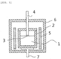
- FIG. 1 is a schematic view illustrating an example of a device for manufacturing a silicon carbide single crystal using a known solution growth process.
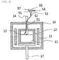
- FIG. 2 is a schematic view of a device for manufacturing a silicon carbide single crystal according to a first embodiment of the present invention.
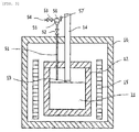
- FIG. 3 is a schematic view of a device for manufacturing a silicon carbide single crystal according to a second embodiment of the present invention.
- the present invention relates to a method for manufacturing a silicon carbide single crystal including coming a seed crystal substrate for growing silicon carbide into contact with a Si-C alloy solution including at least one additive metal and growing the silicon carbide single crystal on a seed crystal for growing silicon carbide using a solution growth process, which includes feeding a silicon feedstock into an alloy solution when a molar ratio of Si and the additive metal is lower than an initially set value as the reaction progresses.
- silicon feedstock includes all raw materials not hindering a reaction of an alloy solution and supplying silicon, and examples thereof may include silicon, a mixture of silicon and carbon, or silicon carbide, but are not limited thereto.
- a typical solution growth process of a silicon carbide single crystal includes coming a silicon carbide seed crystal into contact with a solution having dissolved carbon in a solution including silicon (hereinafter, referred to as 'Si-C solution') to grow the silicon carbide single crystal.
- the silicon carbide seed crystal in contact with the Si-C solution comes into contact with a front end of the seed crystal fixed shaft and drawn by the seed crystal fixed shaft to grow the silicon carbide single crystal from the Si-C solution on the silicon carbide seed crystal.
- the Si-C solution has a low carbon solubility in the solution and a low concentration of silicon carbide in the solution, causing a low growth speed of a crystal.
- the additive metal includes various transition metals or mixtures thereof selected in consideration of the growth speed of the single crystal but is not limited thereto, and examples thereof may include Ti, Cr, Al, Fe, Co, Dy or La.
- Silicon of the alloy solution is a metal element participating in growth of the silicon carbide single crystal, and other metal elements are used as additive metal.
- metals other than silicon are added to reduce a melting point and do not directly participate in the reaction in growth of the silicon carbide single crystal.
- the concentration of silicon of the alloy solution is reduced as the reaction progresses to break the balance of the initially set ratio of Si and additive metal. Therefore, unwillingly, the growth speed of the single crystal is significantly reduced or, in extreme cases, the growth may stop.
- the silicon feedstock is fed into the alloy solution when a molar ratio of Si and the additive metal is lower than an initially set value as the reaction progresses.
- feeding of the silicon feedstock does not mean refeeding or additional feeding of the alloy solution, but means that only the silicon feedstock is fed, if necessary or periodically, into the alloy solution in which the main reaction occurs as the reaction progresses silicon feedstock.
- an amount thereof may be derived using various processes, and illustrative but non-limiting examples of the processes include a process for calculating the molar amount of Si of the alloy solution reduced as the reaction progresses based on a growth thickness of the silicon carbide single crystal and determining the amount of fed silicon within a predetermined range based on the calculated molar amount of Si reduced.
- the alloy solution is substantially melted so as not to include a solid in the crucible, when the silicon feedstock powder is fed, a reaction temperature is reduced or the alloy solution and the silicon feedstock powder are not homogeneously mixed, thus negatively affecting physical properties of the grown single crystal.
- the feeding of a silicon feedstock is performed several times in an amount of up to 0.02 to 15 wt% based on an amount of a silicon element in a crucible in views of melting the additionally fed Si and homogeneity of the grown silicon carbide single crystal.
- the silicon feedstock is fed in the same atmospheric gas as the atmospheric gas in the crucible.
- the atmospheric gas in the crucible is a non-oxidizing atmospheric gas
- examples of the preferable non-oxidizing atmospheric gas may include one or more of gases such as He, Ne, and Ar.
- the inert gas may be used in a mixture form with nitrogen, or carbon-containing gas such as methane.
- the silicon feedstock is added to the alloy solution, it is preferable that the silicon feedstock is fed in the same atmospheric gas as the atmospheric gas in the crucible so as not to hinder the atmosphere in the crucible.
- the silicon feedstock is fed at a pressure that is higher than that of the crucible in the method for manufacturing the silicon carbide single crystal in order to prevent the reaction solution from evaporating.
- a process for feeding the silicon feedstock at a pressure that is higher than that of the crucible may include a process for applying a vacuum, supplying the same gas as the atmospheric gas in the crucible to form a high pressure environment, and feeding the silicon feedstock into the crucible.
- the pressure in the crucible is 0.1 to 1 MPa, and the pressure may be typically an atmospheric pressure.
- silicon and various additive metal elements are added to the graphite crucible having high purity, and heated in an inert gas atmosphere to a set temperature to melt the feedstock.
- the continuous heating of the set temperature is performed to melt carbon in the solution from the crucible and form a silicon carbide solution.
- the continuous heating of the set temperature is performed until a concentration of carbon in the solution reaches a saturation concentration, and a seed crystal is then precipitated in the solution.
- the seed crystal is precipitated, and, after a while, the solution is slowly cooled to grow the silicon carbide single crystal on the seed crystal.
- the silicon feedstock is fed preferably after the temperature in the crucible is increased to 1300°C or more and more preferably after the temperature is increased to 1650°C or more, that is, after the crystal starts to grow in the solution during the growth of SiC.
- a device for feeding the silicon feedstock is not particularly limited, but, for example, a general aspect of the present invention provides a device for manufacturing a silicon carbide single crystal using a solution growth process, which includes a crucible receiving a Si-C alloy solution including at least one additive metal and a seed crystal fixed shaft including a seed crystal substrate for growing silicon carbide, including a silicon feed unit feeding a silicon feedstock into the crucible.
- a device for manufacturing a silicon carbide single crystal includes a crucible receiving an alloy solution (solvent), for example, a graphite crucible, a solvent, an external heater such as a high frequency coil, an insulator, a seed crystal fixed shaft moving upward and downward to support a substrate, and the substrate provided at a front end of the seed crystal fixed shaft.
- solvent for example, a graphite crucible, a solvent, an external heater such as a high frequency coil, an insulator, a seed crystal fixed shaft moving upward and downward to support a substrate, and the substrate provided at a front end of the seed crystal fixed shaft.
- FIG. 1 An embodiment thereof shown in FIG. 1 includes a crucible 2 containing an alloy solution 1 including silicon or additive metal; a seed crystal fixed shaft 4 to which a substrate 3 is attached; a heat emitting body 5; a growth furnace 6; and a lower plate 7 rotating the crucible if necessary.
- the crucible 2 made of a graphite material may be used as a source providing carbon.
- the heat emitting body 5 may be a resistance type heat emitting body or an inductive heating type heat emitting body.
- Inert gas such as argon or helium fills the growth furnace 6, and the degree of vacuum may be typically 100 to 1500 torr.
- a vacuum pump and a gas cylinder for controlling the atmosphere not shown in the drawings may be connected through a valve to the growth furnace 6 to maintain the above atmosphere.
- the seed crystal fixed shaft 4 connected to the substrate may move upward and downward and rotate at a predetermined rate to control a temperature distribution in the crucible. Further, the lower plate 7 supporting the crucible may rotate at predetermined rpm if necessary.
- the general aspect of the present invention provides a device for manufacturing a silicon carbide single crystal including a separate silicon feed unit to feed the silicon feedstock.
- FIG. 2 illustrates a first embodiment of the device for manufacturing the silicon carbide single crystal including the silicon feed unit to feed the silicon feedstock in the general aspect of the present invention.
- the device for manufacturing the silicon carbide single crystal according to the first embodiment is provided in consideration of the rotatable crucible, and the silicon feed unit may include a feed tube having a tube shape formed through at least a portion of the seed crystal fixed shaft.
- elements constituting the silicon feed unit may include a silicon feedstock storage hopper 55, a silicon feedstock feed valve 52 controlling the silicon feedstock to be fed from the silicon feedstock storage hopper 55 to the growth furnace, a silicon feedstock feeding entrance 56 through which the silicon feedstock is supplied to the silicon feedstock storage hopper 55, and a gas connection tube 54 and a gas supply valve 53 controlling the atmosphere in the hopper.
- a manometer 57 may be attached to measure pressure in the hopper.
- a silicon feedstock feed tube 51 is formed through a seed crystal fixed shaft 14 to feed the silicon feedstock from the hopper to the crucible.
- a predetermined amount of silicon feedstock is fed through the silicon feedstock feeding entrance 56 into the silicon feedstock storage hopper, and the feeding entrance is then closed to seal the hopper.
- the silicon feedstock feed valve 52 to the growth furnace is closed.
- the hopper is evacuated through the gas connection tube 54 using an external vacuum pump (not shown).
- the same gas as the atmospheric gas in the growth furnace is supplied through the gas connection tube 54 to maintain a pressure that is higher than that of the growth furnace.
- the gas supply valve 53 is closed, and the silicon feedstock feed valve 52 is opened to feed the silicon feedstock from the hopper to the crucible 12.
- a separate silicon feed unit according to a second embodiment shown in FIG. 3 may include a feed tube separated from the seed crystal fixed shaft for the convenience of installation.
- the device according to the second embodiment has the same constitutional elements and driving method as the device according to the first embodiment, with the exception of the formation position of the silicon feed unit, accordingly, a detailed description thereof is omitted.
- a separate silicon feed unit is provided because a crystal continuously grows even though silicon solids are dispersed in a molten raw material.
- the first and the second embodiments are set forth to illustrate a device for manufacturing a silicon carbide single crystal, but are not construed to limit the technical spirit of providing a silicon feed unit for additionally feeding a silicon feedstock according to the present invention.
Landscapes
- Chemical & Material Sciences (AREA)
- Engineering & Computer Science (AREA)
- Crystallography & Structural Chemistry (AREA)
- Materials Engineering (AREA)
- Metallurgy (AREA)
- Organic Chemistry (AREA)
- Inorganic Chemistry (AREA)
- Crystals, And After-Treatments Of Crystals (AREA)
Abstract
Priority Applications (4)
| Application Number | Priority Date | Filing Date | Title |
|---|---|---|---|
| CN201180051012.1A CN103180493B (zh) | 2010-10-21 | 2011-10-17 | 用于生长碳化硅单晶的方法和装置 |
| JP2013534804A JP5827338B2 (ja) | 2010-10-21 | 2011-10-17 | 炭化珪素単結晶の製造方法及び装置 |
| EP11834582.6A EP2630278B1 (fr) | 2010-10-21 | 2011-10-17 | Procédé de croissance d'un monocristal de carbure de silicium et dispositif afférent |
| US13/880,562 US9359690B2 (en) | 2010-10-21 | 2011-10-17 | Process for growing silicon carbide single crystal and device for the same |
Applications Claiming Priority (2)
| Application Number | Priority Date | Filing Date | Title |
|---|---|---|---|
| KR1020100103046A KR101690490B1 (ko) | 2010-10-21 | 2010-10-21 | 탄화규소 단결정의 제조방법 및 장치 |
| KR10-2010-0103046 | 2010-10-21 |
Publications (2)
| Publication Number | Publication Date |
|---|---|
| WO2012053782A2 true WO2012053782A2 (fr) | 2012-04-26 |
| WO2012053782A3 WO2012053782A3 (fr) | 2012-07-19 |
Family
ID=45975702
Family Applications (1)
| Application Number | Title | Priority Date | Filing Date |
|---|---|---|---|
| PCT/KR2011/007701 Ceased WO2012053782A2 (fr) | 2010-10-21 | 2011-10-17 | Procédé de croissance d'un monocristal de carbure de silicium et dispositif afférent |
Country Status (6)
| Country | Link |
|---|---|
| US (1) | US9359690B2 (fr) |
| EP (1) | EP2630278B1 (fr) |
| JP (1) | JP5827338B2 (fr) |
| KR (1) | KR101690490B1 (fr) |
| CN (1) | CN103180493B (fr) |
| WO (1) | WO2012053782A2 (fr) |
Cited By (3)
| Publication number | Priority date | Publication date | Assignee | Title |
|---|---|---|---|---|
| JP2014189420A (ja) * | 2013-03-26 | 2014-10-06 | Kyocera Corp | 保持体、結晶製造装置および結晶の製造方法 |
| JP2016196402A (ja) * | 2016-05-16 | 2016-11-24 | 京セラ株式会社 | 保持体、結晶製造装置および結晶の製造方法 |
| CN114232097A (zh) * | 2021-12-31 | 2022-03-25 | 广州半导体材料研究所 | 一种制备碳化硅单晶的方法 |
Families Citing this family (14)
| Publication number | Priority date | Publication date | Assignee | Title |
|---|---|---|---|---|
| JP6014258B2 (ja) * | 2014-01-29 | 2016-10-25 | 京セラ株式会社 | 結晶の製造方法 |
| US20170283982A1 (en) * | 2014-09-11 | 2017-10-05 | Nippon Steel & Sumitomo Metal Corporation | METHOD FOR PRODUCING P-TYPE SiC SINGLE CRYSTAL |
| JP2016121028A (ja) * | 2014-12-24 | 2016-07-07 | 京セラ株式会社 | 結晶の製造方法 |
| JP6190070B2 (ja) * | 2015-03-06 | 2017-08-30 | 京セラ株式会社 | 結晶の製造方法 |
| JP6533716B2 (ja) | 2015-08-06 | 2019-06-19 | 信越化学工業株式会社 | SiC単結晶の製造方法 |
| KR102103884B1 (ko) * | 2016-09-30 | 2020-04-23 | 주식회사 엘지화학 | 실리콘카바이드 단결정의 제조 장치 및 제조 방법 |
| CN108166058A (zh) * | 2016-12-07 | 2018-06-15 | 上海新昇半导体科技有限公司 | 4H-SiC晶体生长方法 |
| KR102089460B1 (ko) * | 2017-02-06 | 2020-03-16 | 주식회사 엘지화학 | 실리콘카바이드 단결정의 제조 방법 |
| KR102553771B1 (ko) * | 2018-11-09 | 2023-07-07 | 주식회사 엘지화학 | 실리콘카바이드 단결정의 제조 장치 및 제조 방법 |
| KR102460012B1 (ko) * | 2021-01-19 | 2022-10-28 | 에스케이실트론 주식회사 | 원료 공급 호퍼 |
| CN113718337B (zh) * | 2021-09-03 | 2022-06-03 | 北京晶格领域半导体有限公司 | 一种液相法生长碳化硅晶体的装置及方法 |
| CN114134571B (zh) * | 2021-11-30 | 2023-03-28 | 江苏集芯半导体硅材料研究院有限公司 | 坩埚组件和具有其的单晶生长装置 |
| CN115976625B (zh) * | 2023-02-14 | 2024-03-05 | 中国科学院物理研究所 | 用于制备3C-SiC单晶的方法 |
| CN116497437B (zh) * | 2023-06-25 | 2023-08-18 | 通威微电子有限公司 | 一种碳化硅生长装置和生长方法 |
Citations (4)
| Publication number | Priority date | Publication date | Assignee | Title |
|---|---|---|---|---|
| JP2000264790A (ja) | 1999-03-17 | 2000-09-26 | Hitachi Ltd | 炭化珪素単結晶の製造方法 |
| JP2005179080A (ja) | 2003-12-16 | 2005-07-07 | Sumitomo Metal Ind Ltd | 単結晶の製造方法および製造装置 |
| US20070209573A1 (en) | 2004-09-03 | 2007-09-13 | Sumitomo Metal Industries, Ltd. | Method for preparing silicon carbide single crystal |
| JP2009263178A (ja) | 2008-04-25 | 2009-11-12 | Sumco Corp | 単結晶育成装置および原料供給方法 |
Family Cites Families (17)
| Publication number | Priority date | Publication date | Assignee | Title |
|---|---|---|---|---|
| CA1261715A (fr) * | 1984-07-06 | 1989-09-26 | General Signal Corporation | Methode et dispositif d'epitaxie de mononcristaux de materiaux semiconducteurs, a partir de creusets de faible profondeur, selon la technique de czochralski |
| JPS62260791A (ja) * | 1986-05-08 | 1987-11-13 | Toshiba Ceramics Co Ltd | シリコン単結晶引上装置 |
| DE3644746A1 (de) * | 1986-12-30 | 1988-07-14 | Hagen Hans Dr Ing | Verfahren und vorrichtung zum zuechten von kristallen |
| JPH0383688A (ja) | 1989-08-29 | 1991-04-09 | Konica Corp | 感熱転写記録材料 |
| AU632886B2 (en) * | 1990-01-25 | 1993-01-14 | Ebara Corporation | Melt replenishment system for dendritic web growth |
| JPH06239691A (ja) * | 1993-02-12 | 1994-08-30 | Japan Energy Corp | 単結晶の成長方法 |
| TW503265B (en) * | 1995-12-28 | 2002-09-21 | Mitsubishi Material Silicon | Single crystal pulling apparatus |
| JPH09183688A (ja) * | 1995-12-28 | 1997-07-15 | Mitsubishi Materials Shilicon Corp | 単結晶引上装置 |
| US6706114B2 (en) | 2001-05-21 | 2004-03-16 | Cree, Inc. | Methods of fabricating silicon carbide crystals |
| US7520930B2 (en) * | 2002-04-15 | 2009-04-21 | Sumitomo Metal Industries, Ltd. | Silicon carbide single crystal and a method for its production |
| JP4100228B2 (ja) | 2002-04-15 | 2008-06-11 | 住友金属工業株式会社 | 炭化珪素単結晶とその製造方法 |
| JP4345624B2 (ja) * | 2004-09-21 | 2009-10-14 | 株式会社Sumco | チョクラルスキー法による原料供給装置および原料供給方法 |
| JP2007261844A (ja) * | 2006-03-28 | 2007-10-11 | Sumitomo Metal Ind Ltd | 炭化珪素単結晶の製造方法 |
| CN2913392Y (zh) * | 2006-05-31 | 2007-06-20 | 高殿斌 | 晶体拉晶炉 |
| US8409348B2 (en) * | 2007-03-16 | 2013-04-02 | Ube Industries, Ltd. | Production method of zinc oxide single crystal |
| CA2681353A1 (fr) | 2007-03-19 | 2008-09-25 | Mnk-Sog Silicon, Inc. | Procede et appareil de fabrication d'un lingot de silicium |
| WO2008133278A1 (fr) * | 2007-04-24 | 2008-11-06 | Sumco Techxiv Corporation | Procédé de fabrication d'un monocristal de silicium, appareil pour la mise en œuvre de ce procédé et lingot de monocristal de silicium |
-
2010
- 2010-10-21 KR KR1020100103046A patent/KR101690490B1/ko not_active Expired - Fee Related
-
2011
- 2011-10-17 WO PCT/KR2011/007701 patent/WO2012053782A2/fr not_active Ceased
- 2011-10-17 US US13/880,562 patent/US9359690B2/en active Active
- 2011-10-17 EP EP11834582.6A patent/EP2630278B1/fr not_active Not-in-force
- 2011-10-17 JP JP2013534804A patent/JP5827338B2/ja not_active Expired - Fee Related
- 2011-10-17 CN CN201180051012.1A patent/CN103180493B/zh not_active Expired - Fee Related
Patent Citations (4)
| Publication number | Priority date | Publication date | Assignee | Title |
|---|---|---|---|---|
| JP2000264790A (ja) | 1999-03-17 | 2000-09-26 | Hitachi Ltd | 炭化珪素単結晶の製造方法 |
| JP2005179080A (ja) | 2003-12-16 | 2005-07-07 | Sumitomo Metal Ind Ltd | 単結晶の製造方法および製造装置 |
| US20070209573A1 (en) | 2004-09-03 | 2007-09-13 | Sumitomo Metal Industries, Ltd. | Method for preparing silicon carbide single crystal |
| JP2009263178A (ja) | 2008-04-25 | 2009-11-12 | Sumco Corp | 単結晶育成装置および原料供給方法 |
Non-Patent Citations (1)
| Title |
|---|
| See also references of EP2630278A4 |
Cited By (3)
| Publication number | Priority date | Publication date | Assignee | Title |
|---|---|---|---|---|
| JP2014189420A (ja) * | 2013-03-26 | 2014-10-06 | Kyocera Corp | 保持体、結晶製造装置および結晶の製造方法 |
| JP2016196402A (ja) * | 2016-05-16 | 2016-11-24 | 京セラ株式会社 | 保持体、結晶製造装置および結晶の製造方法 |
| CN114232097A (zh) * | 2021-12-31 | 2022-03-25 | 广州半导体材料研究所 | 一种制备碳化硅单晶的方法 |
Also Published As
| Publication number | Publication date |
|---|---|
| JP2013540094A (ja) | 2013-10-31 |
| CN103180493B (zh) | 2016-08-17 |
| WO2012053782A3 (fr) | 2012-07-19 |
| EP2630278A2 (fr) | 2013-08-28 |
| JP5827338B2 (ja) | 2015-12-02 |
| KR101690490B1 (ko) | 2016-12-28 |
| US20130305982A1 (en) | 2013-11-21 |
| KR20120041549A (ko) | 2012-05-02 |
| US9359690B2 (en) | 2016-06-07 |
| CN103180493A (zh) | 2013-06-26 |
| EP2630278B1 (fr) | 2015-10-07 |
| EP2630278A4 (fr) | 2014-06-18 |
Similar Documents
| Publication | Publication Date | Title |
|---|---|---|
| EP2630278A2 (fr) | Procédé de croissance d'un monocristal de carbure de silicium et dispositif afférent | |
| WO2013002539A2 (fr) | Appareil et procédé de croissance de monocristal de carbure de silicium | |
| WO2013002540A2 (fr) | Appareil et procédé de croissance de monocristal de carbure de silicium | |
| KR101235772B1 (ko) | 탄화규소 단결정의 성장방법 | |
| US9856582B2 (en) | SiC single crystal and production method thereof | |
| EP2881499B1 (fr) | Procédé de croissance de cristaux de carbure de silicium | |
| WO2013100456A1 (fr) | Poudre de carbure de silicium, son procédé de fabrication et procédé de croissance d'un cristal unique | |
| US20130247334A1 (en) | Crucible for Solidifying a Silicon Ingot | |
| WO2014126273A1 (fr) | Dispositif de préparation d'une nanostructure mox de haute pureté et procédé de préparation correspondant | |
| JP4135239B2 (ja) | 半導体結晶およびその製造方法ならびに製造装置 | |
| WO2020080856A1 (fr) | Procédé de régénération de sous-produit de carbure de silicium produit par un processus de dépôt en une matière première monocristallinne | |
| CN119900087B (zh) | 一种高效率碳化硅单晶生长方法 | |
| JP2010030891A (ja) | 化合物半導体結晶 | |
| JP2008239480A5 (fr) | ||
| WO2016068583A1 (fr) | Appareil de fabrication de lingot | |
| KR20190031036A (ko) | 실리콘카바이드 단결정의 제조 장치 | |
| US20130263774A1 (en) | Seed material for liquid phase epitaxial growth of monocrystalline silicon carbide, and method for liquid phase epitaxial growth of monocrystalline silicon | |
| WO2013015642A2 (fr) | Procédé de développement d'un lingot | |
| CN116815318B (zh) | 一种制备高纯度SiC多晶粉体的装置和方法 | |
| WO2021080382A1 (fr) | Méthodes de préparation de poudre de carbure de silicium et carbure de silicium monocristallin | |
| CN102951931A (zh) | 制备SiC涂层的方法 | |
| JP2008001569A (ja) | 単結晶SiC及びその製造方法並びに単結晶SiCの製造装置 | |
| KR20070072670A (ko) | 단결정 성장 장치 및 단결정 성장 방법 | |
| KR102302753B1 (ko) | 실리콘계 용융 조성물 및 이를 이용하는 실리콘카바이드 단결정의 제조 방법 | |
| US20090205561A1 (en) | METHOD FOR PRODUCING SILICON CARBIDE (SiC) CRYSTAL AND SILICON CARBIDE (SiC) CRYSTAL OBTAINED BY THE SAME |
Legal Events
| Date | Code | Title | Description |
|---|---|---|---|
| 121 | Ep: the epo has been informed by wipo that ep was designated in this application |
Ref document number: 11834582 Country of ref document: EP Kind code of ref document: A2 |
|
| ENP | Entry into the national phase |
Ref document number: 2013534804 Country of ref document: JP Kind code of ref document: A |
|
| NENP | Non-entry into the national phase |
Ref country code: DE |
|
| WWE | Wipo information: entry into national phase |
Ref document number: 2011834582 Country of ref document: EP |
|
| WWE | Wipo information: entry into national phase |
Ref document number: 13880562 Country of ref document: US |