WO2012063902A1 - Dispositif de contrôle de la variation de résistance sous champ électrique de dispositifs électroniques et procédé de détection de la variation de résistance sous champ électrique de dispositifs électroniques - Google Patents
Dispositif de contrôle de la variation de résistance sous champ électrique de dispositifs électroniques et procédé de détection de la variation de résistance sous champ électrique de dispositifs électroniques Download PDFInfo
- Publication number
- WO2012063902A1 WO2012063902A1 PCT/JP2011/075943 JP2011075943W WO2012063902A1 WO 2012063902 A1 WO2012063902 A1 WO 2012063902A1 JP 2011075943 W JP2011075943 W JP 2011075943W WO 2012063902 A1 WO2012063902 A1 WO 2012063902A1
- Authority
- WO
- WIPO (PCT)
- Prior art keywords
- electronic device
- electric field
- fluctuation
- electrode
- inspecting
- Prior art date
- Legal status (The legal status is an assumption and is not a legal conclusion. Google has not performed a legal analysis and makes no representation as to the accuracy of the status listed.)
- Ceased
Links
Images










Classifications
-
- G—PHYSICS
- G01—MEASURING; TESTING
- G01R—MEASURING ELECTRIC VARIABLES; MEASURING MAGNETIC VARIABLES
- G01R31/00—Arrangements for testing electric properties; Arrangements for locating electric faults; Arrangements for electrical testing characterised by what is being tested not provided for elsewhere
- G01R31/28—Testing of electronic circuits, e.g. by signal tracer
- G01R31/2851—Testing of integrated circuits [IC]
- G01R31/2855—Environmental, reliability or burn-in testing
- G01R31/2872—Environmental, reliability or burn-in testing related to electrical or environmental aspects, e.g. temperature, humidity, vibration, nuclear radiation
- G01R31/2879—Environmental, reliability or burn-in testing related to electrical or environmental aspects, e.g. temperature, humidity, vibration, nuclear radiation related to electrical aspects, e.g. to voltage or current supply or stimuli or to electrical loads
-
- G—PHYSICS
- G01—MEASURING; TESTING
- G01R—MEASURING ELECTRIC VARIABLES; MEASURING MAGNETIC VARIABLES
- G01R31/00—Arrangements for testing electric properties; Arrangements for locating electric faults; Arrangements for electrical testing characterised by what is being tested not provided for elsewhere
- G01R31/001—Measuring interference from external sources to, or emission from, the device under test, e.g. EMC, EMI, EMP or ESD testing
-
- G—PHYSICS
- G01—MEASURING; TESTING
- G01R—MEASURING ELECTRIC VARIABLES; MEASURING MAGNETIC VARIABLES
- G01R31/00—Arrangements for testing electric properties; Arrangements for locating electric faults; Arrangements for electrical testing characterised by what is being tested not provided for elsewhere
- G01R31/28—Testing of electronic circuits, e.g. by signal tracer
- G01R31/30—Marginal testing, e.g. by varying supply voltage
-
- G—PHYSICS
- G01—MEASURING; TESTING
- G01R—MEASURING ELECTRIC VARIABLES; MEASURING MAGNETIC VARIABLES
- G01R29/00—Arrangements for measuring or indicating electric quantities not covered by groups G01R19/00 - G01R27/00
- G01R29/12—Measuring electrostatic fields or voltage-potential
-
- G—PHYSICS
- G01—MEASURING; TESTING
- G01R—MEASURING ELECTRIC VARIABLES; MEASURING MAGNETIC VARIABLES
- G01R29/00—Arrangements for measuring or indicating electric quantities not covered by groups G01R19/00 - G01R27/00
- G01R29/08—Measuring electromagnetic field characteristics
- G01R29/0807—Measuring electromagnetic field characteristics characterised by the application
- G01R29/0814—Field measurements related to measuring influence on or from apparatus, components or humans, e.g. in ESD, EMI, EMC, EMP testing, measuring radiation leakage; detecting presence of micro- or radiowave emitters; dosimetry; testing shielding; measurements related to lightning
-
- G—PHYSICS
- G01—MEASURING; TESTING
- G01R—MEASURING ELECTRIC VARIABLES; MEASURING MAGNETIC VARIABLES
- G01R31/00—Arrangements for testing electric properties; Arrangements for locating electric faults; Arrangements for electrical testing characterised by what is being tested not provided for elsewhere
- G01R31/28—Testing of electronic circuits, e.g. by signal tracer
- G01R31/302—Contactless testing
- G01R31/312—Contactless testing by capacitive methods
Definitions
- the present invention relates to a technique for inspecting resistance when a variable electric field is exposed to an electronic device.
- This resistance test is defined by the international standard IEC61000-4-2 and its related standards (ISO10605, JASO D101) and the like, and generally, an ESD test apparatus using an ESD gun is used.
- This ESD test apparatus makes the ESD gun contact terminal (discharge rod) contact the conductive area of the object to be measured, such as an electronic device with the power turned on, and pulls the trigger switch of the ESD gun. To generate contact discharge.
- the surface of the object to be measured is an insulator, the contact terminal of the ESD gun with the trigger switch pulled is brought close to the object to be measured and discharged in the air.
- ESD is applied to the object to be measured from the outside, and its influence is observed.
- it is checked whether or not the device under test operates normally, whether or not it returns to normal even if an instantaneous malfunction occurs.
- a horizontal coupling plate and a vertical coupling plate are arranged around the object to be measured, and ESD is applied to them to test the resistance against indirect discharge.
- a similar malfunction may occur in a control panel of a control room such as a power plant, air traffic control, or chemical plant.
- An operator usually sits on a chair and operates the control panel, but when he stands up from the chair and tries to operate a high place, a malfunction occurs.
- the electrostatic capacity of the operator sitting in the chair is considered to be approximately 300 pF, but decreases to about 100 pF when standing up.
- the electrostatic capacity is reduced to one third, the potential of the operator jumps up to three times in an instant. This potential fluctuation of the operator may cause inductive charging in the electronic equipment inside the control panel and induce a malfunction, similarly to the above-described passing operation of the automatic ticket gate.
- this ESD test apparatus is a direct discharge phenomenon that occurs when an electronic device (object to be measured) comes into contact with the outside (the human body to be operated), or indirectly that occurs around the electronic device. This is to inspect the resistance to a general discharge phenomenon.
- a malfunction occurs due to a discharge phenomenon that occurs inside the electronic device.
- the present invention has been made in view of the above problems, and has an object to provide a variable electric field resistance inspection technique for inspecting malfunction caused by a discharge phenomenon occurring inside an electronic device, which cannot be inspected by a conventional ESD test apparatus. Yes.
- the above object can be achieved by the following means based on the earnest research of the present inventors.
- the present invention that achieves the above object includes an application electrode for exposing an electric field to an electronic device to be measured, and an electric field that varies the strength of the electric field applied to the electronic device during inspection.
- a variable electric field resistance of the electronic device wherein the operation characteristic of the electronic device is inspected by causing inductive charging inside the electronic device due to the fluctuation of the electric field during the inspection. Inspection equipment.
- the electric field variation means further includes a voltage control device that varies the strength of the electric field by changing a voltage applied to the application electrode. It is characterized by that.
- the electric field fluctuation means further increases the absolute value of the positive or negative electric field applied to the electronic device, thereby increasing the absolute value of the electric device.
- the potential of the first induction charging of the electronic device is reset (returned to the ground potential), and further, the absolute value of the positive or negative electric field is decreased,
- the second induction charging in which the first induction charging and the positive / negative are reversed is generated for the electronic device.
- a plurality of the applied electrodes are further arranged.
- the object to be measured is assumed to be a hexahedron, a first application electrode disposed opposite to the first surface of the hexahedron; And a second application electrode disposed opposite to the second surface of the hexahedron.
- a plurality of the application electrodes are arranged to face the first surface of the hexahedron. It is characterized by that.
- a common field emission surface is formed by arranging a plurality of field emission surfaces of the application electrodes side by side. .
- the electric field fluctuating means further applies a voltage with different timings to the plurality of application electrodes, so that each application electrode has a timing.
- the different electric fields are applied to the electronic device.
- the electric field variation means further varies the electric field of the plurality of application electrodes independently, thereby (local) in the vicinity of the electronic device. It is characterized by controlling the gradient of the electric field in the space.
- the plurality of applied electrodes are further embedded in a single insulator.
- the application electrode is a plate electrode, and a plane of the plate electrode is opposed to the electronic device.
- the application electrode is a plate electrode, and an end surface of the plate electrode is opposed to the electronic device.
- the application electrode is a rod-shaped electrode, and a side surface extending in the longitudinal direction of the rod-shaped electrode is opposed to the electronic device.
- the application electrode further includes a plurality of strip-shaped field emission surface pieces facing the electronic device, and the plurality of field emission surface pieces are arranged side by side. Thus, one field emission surface is formed.
- the application electrode further includes a plurality of plate-like electrode pieces, and the plane of the plate-like electrode piece is the strip-shaped field emission surface piece. It is characterized by becoming.
- the application electrode further includes a plurality of plate-like electrode pieces, and an end surface of the plate-like electrode piece is the strip-like field emission surface piece. It is characterized by becoming.
- the application electrode further includes a plurality of rod-shaped electrode pieces, and a side surface extending in a longitudinal direction of the rod-shaped electrode piece has the band-shaped field emission. It is a surface piece.
- the application electrode further includes a band-shaped protrusion, and a protruding end of the band-shaped protrusion is the band-shaped field emission surface piece.
- the electric field variation means further includes a moving mechanism that changes a relative distance between the electronic device and the application electrode. It is characterized by varying the strength and gradient of the electric field.
- the apparatus for inspecting variable electric field resistance of an electronic device that achieves the above object is characterized by further comprising discharge detection means for detecting a discharge phenomenon that occurs inside the electronic device due to the induction charging.
- the apparatus further comprises a synchronization control means for synchronizing the sensing timing of the discharge detection means with the fluctuation timing of the electric field by the electric field fluctuation means.
- a high resistance material is further used as a material for the application electrode.
- a high-resistance rubber material is further used for the wiring for supplying a voltage to the applied electrode.
- the present invention that achieves the above object is to apply an electric field from the outside to an electronic device as an object to be measured using an application electrode, and to change the strength and gradient of the electric field applied to the electronic device.
- a method for inspecting a variation electric field resistance of an electronic device is characterized in that induction charging is generated inside the electronic device and operation characteristics of the electronic device due to the induction charging are inspected.
- the method further comprises detecting a discharge phenomenon generated inside the electronic device due to the induction charging, and inspecting an operating characteristic of the electronic device due to the discharge phenomenon.
- the strength of the electric field applied to the electronic device is further varied by changing a voltage supplied to the application electrode.
- the strength and gradient of the electric field applied to the electronic device are further varied by changing a relative distance between the application electrode and the electronic device. It is characterized by that.
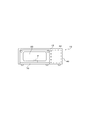
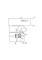
- FIG. 1 shows an experimental facility 1 for this verification.
- this experimental facility 1 two large and small copper plates 3 and 4 are arranged in a plastic case 2 with a gap of 0.05 mm.
- the gap is not limited to 0.05 mm, and may be about 0.5 mm depending on the level of the induced voltage.
- the spark discharge is based on Paschen's law, it is better to be as narrow as possible. This is because if the atmospheric pressure is constant, the narrower the gap, the lower the voltage is discharged.
- a distance of 20 mm is provided below the copper plates 3 and 4, and the coaxial cable 5 connecting the probe portion (tip portion) of the differential probe and the oscilloscope is parallel to the plastic case 2.
- the separation distance 20 mm is not limited to this, and may be further separated as long as a sufficient reception voltage is generated.
- the detection band of the differential probe is set to 400 MHz, and a digital oscilloscope 6 is connected to the coaxial cable 5 of the differential probe output to analyze a noise waveform detected at the time of discharge.
- the signal input terminal at the tip of the differential probe, the + side and the ⁇ side are short-circuited with an extremely short copper wire so that no input signal is input.
- the large and small copper plates 3 and 4 are not grounded to the ground and are not in contact with surrounding conductors.
- a fluctuating electric field generated by manually moving a charged Teflon (registered trademark) or plastic charging plate 7 from the right to the left or from the left to the right near the upper surface of the plastic case 2 is plastic.
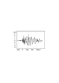
- a waveform detected by the digital oscilloscope 6 is shown in FIG. In this waveform, since the vibration has a period of 1 nanosecond or less and the amplitude is 10 V or more, a discharge is generated between the copper plates 3 and 4.
- the input portion at the tip of the differential probe is short-circuited between the + side and the ⁇ side, no input signal is input to the differential probe. Accordingly, a signal having such a large amplitude should not be generated, but such a large noise signal is detected.
- the spark discharge is a discharge that ends at a very high speed in a short time, and emits a broadband electromagnetic wave (electromagnetic noise) including a frequency component of several GHz or more.
- the coaxial noise of the differential cable is received by the electromagnetic noise, and the common mode signal is converted into the normal mode and analyzed by an oscilloscope to obtain the waveform of FIG.
- the Teflon (registered trademark) charging plate 7 is negatively charged and the plastic charging plate 7 such as acrylic has a property of being easily positively charged.
- the fluctuation electric field tolerance inspection apparatus has a floating conductor that is unintentionally present inside the electronic device or electronic device to be inspected, and the electric field around the electronic device or electronic device fluctuates. It is characterized in that it is inductively charged, and a rapid discharge (spark discharge) between this and its peripheral conductors and the presence or absence of malfunction caused by the discharge are inspected, and a countermeasure is provided.
- the main trouble that the present invention is subject to inspection is that an electronic device malfunctions even though direct ESD to the electronic device or indirect ESD around the device has not occurred. It is a phenomenon like this. That is, a phenomenon in which an operator of an electronic device or a charged object in the vicinity does not contact the electronic device to be inspected (no discharge has occurred with respect to the electronic device) and causes a malfunction. Electrostatic discharge that induces malfunctions occurs inside electronic equipment and occurs in a narrow gap between adjacent metal conductors, so the frequency components contained in the emitted transient electromagnetic waves are extremely wide (several GHz or more). ) And very strong, and the electric field strength easily reaches the order of kV / m.
- an LSI for example, a CPU or IC
- LSI for example, a CPU or IC
- Such troubles are considered to be detected, evaluated, and countermeasures only by the method using the variable electric field resistance inspection apparatus according to the present invention.
- Avionics and defense equipment take strict defense measures against electromagnetic interference (EMI) caused by radar waves, but the electric field strength of the electromagnetic wave irradiation test (example: RTCA DO-160E) is the basis for this.
- the maximum is 600 V / m (0.4 GHz to 18 GHz).
- this value is comparable to the electric field intensity when irradiated from a 1000 kW (1 MW) pulse radar at a distance of 10 m from the device, the method we propose this time exceeds 1 kV / m inside the device.
- An electric field strength can be generated, making it possible to test its resistance. Further, according to the present invention, there is no need for an expensive and large anechoic chamber, a high power power amplifier, a radiating antenna or the like.
- the discharge gap is about 0.05 mm
- the spectrum distribution observed by the spectrum analyzer is well over 18 GHz, and the impulse for driving the floating conductor (small dipole) It has been found that the rise of the current is very fast (estimated less than 40 ps) and has a large amplitude (depending on the amount of charge, on the order of tens of A to 100 A).
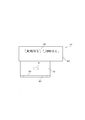
- FIG. 3A is a front view of the inspection apparatus
- FIG. 3B is a top view of the inspection apparatus
- FIG. 3C is a side view of the inspection apparatus
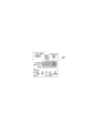
- FIG. 3D is a control panel of the main body of the inspection apparatus.
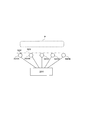
- the inspection apparatus 10 includes a main body 15, an application electrode 20, an electric field variation unit 30, a casing 40, a discharge detection unit (described later), a synchronization control unit 60, and a mounting table 70.
- An electric field fluctuation unit 30, a discharge detection unit (described later), and a synchronization control unit 60 are accommodated in the housing 40 of the main body 15.
- the application electrode 20 applies one positive or negative electric field from the outside to the electronic device P to be measured in a non-contact state.
- the application electrode 20 has a so-called plate shape (plate shape), and this plane is a field emission surface 22.
- the application electrode 20 is fixed in a standing state on the mounting table 70 so that the field emission surface 22 faces the side surface of the electronic device P.
- the mounting table 70 is horizontally arranged so as to protrude from the side surface of the main body 15, and at least the upper surface is made of an insulator.
- An electronic device P is disposed in the center of the mounting table 70.
- the electric field variation means 30 is a voltage control device and is accommodated in the housing 40.
- the electric field variation means 30 varies the strength of the electric field generated from the application electrode 20 without changing the polarity by changing the DC voltage applied to the application electrode 20. Thereby, the strength of the electric field applied to the electronic device P during the inspection can be changed over time without changing the polarity. If a floating conductor (a conductor that is not grounded) exists inside the electronic device P, when the electric field applied to the electronic device P is varied, induction charging occurs in the floating conductor. In the inspection apparatus 10, whether or not there is a structure that generates a spark discharge in and around the electronic device P by forcibly generating this inductive charge in the electronic device P, and thereby the electronic device P malfunctions.
- the operational characteristics such as whether or not to perform can be verified. Specifically, when the other conductor is arranged close to the floating conductor inside the electronic device P, a discharge phenomenon may occur between the two as shown in the verification example. By providing an environment in which this discharge is forcibly generated, the presence or absence of the discharge is verified, and at the same time, the resistance to noise is inspected.
- a control panel 42 (see FIG. 3D) is prepared in the casing 40 of the main body 15.
- the control panel 42 includes a radiation voltage setting unit (Test Voltage), an inspection start button (Start), an inspection end button (Stop), and a repetition setting unit for setting the number of tests (number of voltage applications) within a range of 0 to 9 times ( (Repetition), application time setting unit (Timing) that sets the application timing (delay timing) of the voltage supplied to each electrode in the case of multiple electrodes specification within the range of 0.1 to 1 second, and the application slope of the same voltage is 0 .Slope setting section (Ramp) set within the range of 1 to 1 second, connector section (Output) for connecting the wiring for supplying voltage to each electrode, polarity setting section (Polarity) for switching the polarity of the high voltage electric field, electronic equipment Multi-axis movement to move the terminal (FG) that supplies the ground potential to the inspection head jig, discharge detection probe connection connector (Disc. Probe), charge potential detection probe connection connector (
- Radiation voltage setting section sets the applied voltage within the range of 0 to -25 kV or 0 to +25 kV.
- the inspection start button (Start) and the inspection end button (Stop) are buttons for manually starting and ending the test.
- the number of times set in the repeat setting section (Repetition) is set to 0, the test is repeatedly performed from when the inspection start button (Start) is pressed until the inspection end button (Stop) is pressed.
- the number of tests voltage application count
- the test is automatically terminated when the test collection is completed.
- a discharge detection probe serving as a discharge detection means is connected to a connector (Disc. Probe) of the discharge detection probe.
- This discharge detection probe receives and amplifies and detects an electromagnetic wave emitted by discharge, and notifies the user by an alarm sound or LED display.
- a function of transmitting this detection signal to the main body 15 and recording it as a history may be incorporated.
- a charging detection antenna (not shown) is connected to the connector (V probe) of the charging potential detection probe. The electrification detection antenna detects electric field fluctuations, further amplifies and then performs signal processing to detect electrification. Note that these discharge detection and charged potential detection functions can be incorporated in the main body 15.
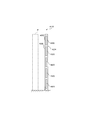
- FIG. 4A schematically shows the time variation of the electric field emitted from the application electrode 30 by the electric field variation means 30, and FIG. 4B schematically illustrates the time variation of the induction charging acting on the electronic device P. It is shown.
- the electric field variation means 30 gradually increases the absolute value of one of the positive and negative DC voltages applied to the application electrode 20 to generate an electric field E1 that is an increase region from the application electrode 20.
- the electric field E1 is set to be positive.
- a positive induction charging T1 that gradually increases occurs in the electronic device P.
- discharge and malfunction when the positive first induction charging T1 occurs in the electronic device P are inspected.
- the first induction charging T1 of the electronic device P is grounded while the electric field E1 of the application electrode 20 is maintained, so that the potential is once reset. Further, by reducing the absolute value of the positive or negative voltage applied to the application electrode 20 until it becomes 0 V, an electric field E2 that is a decrease region is generated from the application electrode 20. As a result, a negative second induction charging T2 that is gradually increased and opposite to the first induction charging T1 is generated for the electronic device P. By this operation, discharge and malfunction when negative second induction charging T2 occurs in the electronic device P are inspected.
- the electric field variation means 30 can adjust the voltage (radiation voltage) within the range of ⁇ 25 kV to +25 kV with respect to the application electrode 20, and can generate both positive and negative electric fields.
- the voltage supply repetition rate can be adjusted in the range of 2 to 10 seconds / time.
- the slope of the applied electric field can be controlled from 0.1 second to 1 second.
- the induction charging reset in the electronic device P is connected to a ground terminal (FG) capable of switching the ground state ON / OFF to the electronic device P. It is preferable to forcibly reset the electric field changing means 30 by switching the ground terminal ON / OFF.
- the intensity (absolute value) of the electric field applied to the electronic device P reaches a certain level (voltage determined by the gap between adjacent conductors and other conditions)
- the electric discharge is spontaneously generated. May be controlled so as to stop increasing the voltage and start decreasing. In this way, the ON / OFF switch for the ground terminal can be omitted.
- the synchronization control means 60 synchronizes the sensing timing of the discharge detection means with the electric field fluctuation timing by the electric field fluctuation means 30. This is because in one inspection, it is necessary to repeatedly apply an electric field to the electronic device P to detect the presence or absence of the discharge state.
- the number of repetitions of electric field application can be selected within a range of 1 to 9, or a pattern to be continuously applied can be selected until forced stop.
- a situation in which a so-called charged body approaches or leaves the electronic device P from the outside can be created in a pseudo manner.
- malfunction of the electronic device P can be inspected based on a phenomenon in which clothes or a human body charged with static electricity approaches or leaves the electronic device P.
- this inspection apparatus 10 since the electric field intensity generated from the application electrode 20 is increased or decreased, a situation where the charged body approaches or separates virtually is created, so that the apparatus structure is greatly simplified, and Stable inspection is possible.
- the inspection apparatus 10 it is possible to verify the discharge phenomenon generated inside the electronic device P due to the fluctuation of the external electrostatic field, not the direct discharge using the conventional ESD gun. Therefore, it is possible to guarantee the operation assuming the movement of the user (electrostatic field holder) who operates the electronic device P, and the safety of the electronic device P can be further enhanced.
- the number of discharge phenomena generated inside the electronic device P by the discharge detection means, the magnitude of the amplitude (noise intensity) when the discharge waveform is detected, and the actual malfunction of the electronic device P What is necessary is just to verify the electric field tolerance of the electronic device P using information, such as whether it has produced, suitably.
- FIGS. 5A and 5B are a side view of the inspection apparatus 110
- FIG. 5B is a top view. Note that the last two digits of the reference numerals used in the illustration and description of the inspection apparatus 110 are the same as the reference numerals of the inspection apparatus 10 of the first embodiment, thereby omitting redundant description. The difference will be mainly described.
- the inspection apparatus 110 includes a moving mechanism 180 that changes the relative distance S between the electronic device P and the application electrode 120 as the electric field control means 130.
- the intensity of the electric field applied to the electronic device P is changed by the change in the relative distance S.
- the moving mechanism 180 includes an X-axis guide 182 disposed in the horizontal direction, a Y-axis guide 184 disposed on the X-axis guide 182, and a Z-axis rotation motor 186 disposed on the Y-axis guide 184. And an arm member 188 held by the Z-axis rotation motor 186. An application electrode 120 is fixed to the tip of the arm member 188. It is also possible to realize a three-axis movement by further adding a Z-axis guide for controlling the movement in the height direction (Z direction).
- the X axis guide 182 conveys the Y axis guide 184 in the X axis direction
- the Y axis guide 184 conveys the Z axis rotation motor 186 in the Y axis direction.
- the Z axis rotation motor 186 rotates the arm member 188.
- this inspection apparatus 110 it is possible to move the charged body closer to or away from the electronic device P from various directions and angles, thereby changing the electric field applied to the electronic device P. Can do. For example, a situation in which a person wearing easily charged clothes such as chemical fibers passes through an automatic ticket gate can be verified in a pseudo manner. In other words, according to the present inspection apparatus 110, it is possible to simulate various electric field fluctuation patterns to cause inductive charging in the electronic device P and confirm whether or not a malfunction occurs.
- the present invention is not limited to this, for example, in addition to the change of the relative distance S
- the present invention is not limited to this, for example, in addition to the change of the relative distance S
- by changing the supply voltage to the application electrode 120 as shown in the first embodiment it is possible to perform more advanced electric field control.
- the case where the relative distance S between the electronic device P and the application electrode 120 is changed by moving the application electrode 120 using the movement mechanism 180 is illustrated, but of course, the electronic device P side is moved to the movement mechanism 180.
- the relative distance S between the electronic device P and the application electrode 120 may be changed.
- the relative distance S between them can be changed.
- FIGS. 6A and 6B are views of the inspection apparatus 210
- FIG. 6B is a side view. Note that the last two digits of the reference numerals used in the illustration and description of the inspection apparatus 210 are the same as the reference numerals of the inspection apparatus 10 of the first embodiment, thereby omitting redundant description. The difference will be mainly described.
- first to third application electrodes 220A to 220C are arranged.
- the first application electrode 220A is disposed to face the first surface of the hexahedron
- the second application electrode 220B is perpendicular to the first surface of the hexahedron
- the third application electrode 220C is arranged to face the third surface that is perpendicular to both the first surface and the second surface of the hexahedron.
- the DC voltage applied to the first to third application electrodes 220A to 220C is shifted while shifting the timing (phase), for example, from the first application electrode 220A to the second application voltage. It is possible to verify the electric field fluctuation that moves to the application electrode 220B side. In addition, by verifying the situation in which the charged body approaches or leaves the electronic device P simultaneously from a plurality of directions by simultaneously supplying voltages to the first to third application electrodes 220A to 220C. Is also possible.
- FIG. 7A is a top view of the inspection apparatus 310
- FIG. 7B is a graph of a voltage control timing waveform in the inspection apparatus 310.
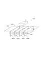
- the inspection device 310 is arranged such that all of the first to fifth application electrodes 320A to 320E face one surface of the electronic device P. Further, these first to fifth application electrodes 320 A to 320 E are embedded in one insulator 324. As a result, the field emission surface 322 formed by the plurality of application electrodes 320A to 320E is connected to form one common field emission surface 328. In the common field emission surface 328, since the potential can be partially changed, a gradient can be formed in the electric field generated in the space near the electronic device P.
- the insulator 324 is in the form of a sheet made of nylon or the like, and the internal first to fifth application electrodes 320A to 320E are preferably made of a flexible high resistance material such as conductive rubber. Accordingly, the first to fifth application electrodes 320A to 320E are insulated from each other.
- the electric field fluctuation means 330 controls the supply voltages to the first to fifth application electrodes 320A to 320E independently of each other. As shown in FIG. 7B, a voltage with a shifted timing is applied to the first to fifth application electrodes 320A to 320E. As a result, the first to fifth application electrodes 320A to 320E can apply electric fields having different timings to the electronic device P. That is, an electric field that moves in the order of the first to fifth application electrodes 320A to 320E along the surface direction of the field emission surface 322 can be applied to the electronic device P. Note that the voltage supply waveforms are preferably overlapped with each other between adjacent application electrodes, and an electric field that moves smoothly can be created.
- the first to fifth application electrodes 320A to 320E are arranged on the side surface of the automatic ticket gate, and a varying electric field is applied. As a result, it becomes possible to artificially create a situation in which a user with static electricity walks and passes through the side of the automatic ticket gate.
- the third application electrode 320C is closest to the electronic device P as shown in FIG. 8A, for example.
- the first and fifth application electrodes 320A and 320E may be arranged in a V shape so that they are farthest from each other. If the voltage is controlled as shown in FIG. 7B in such a state, it is possible to create an environment in which the electric field approaches and moves away from the electronic device P.
- the first to fifth application electrodes 320A to 320E can be arranged along the V shape or the arc shape so as to surround the electronic device P.
- first to fifth application electrodes 320A to 320E are covered with an insulator, it is possible to inspect them while they are attached to the electronic device P. By pasting, the applied electric field can be strengthened even when the voltage is low.
- first to fifth application electrodes 320A to 320E are plate-shaped (plate-shaped), and these planes become the field emission surface 322 and are opposed to the electronic device P is illustrated.
- the end surfaces of the first to fifth application electrodes 320A to 320E are also preferable to arrange the end surfaces of the first to fifth application electrodes 320A to 320E as field emission surfaces 322 so that the end surfaces face the electronic device P.
- the plurality of field emission surfaces 322 are connected to form one common field emission surface 328. Since the density of the lines of electric force is increased on the end face of the plate as compared with the plane of the plate serving as the electrode, it is possible to efficiently induce induction charging for the electronic device P.
- first to fifth application electrodes 320A to 320E are plate-shaped (plate-shaped) is illustrated, but as shown in FIG. 8D, these are used as rod-shaped electrodes, and side surfaces extending in the longitudinal direction. Is preferably opposed to the electronic device P. Since the density of the electric lines of force is increased on the side surface of the rod-shaped electrode, it is possible to efficiently induce induction charging to the electronic device P.
- FIGS. 9A and 9B are a side view of the inspection apparatus 410
- FIG. 9B is a front view of the inspection apparatus 410. Note that the last two digits of the reference numerals used in the illustration and description of the inspection apparatus 410 are the same as the reference numerals of the inspection apparatus 10 of the first embodiment, thereby omitting redundant description. The difference will be mainly described.
- a total of 25 application electrodes 420 are arranged in a matrix so as to face one surface of the electronic device P. Further, these application electrodes 420 are embedded in one insulator 424. As a result, the field emission surface 422 by the plurality of application electrodes 420 is connected to form one common field emission surface 428. In the common field emission surface 428, since the potential can be changed in a matrix shape over the entire surface direction, the electric field generated in the space near the electronic device P can be freely adjusted in a two-dimensional direction. A gradient can be formed.
- electric field fluctuation means controls the supply voltages to these application electrodes 420 independently of each other. Specifically, the voltage is controlled so that the electric field moves in the vertical direction along the surface direction of the field emission surface 422.
- the inspection device 410 is disposed in front of the control panel, and an electric field that varies in the vertical direction is applied. As a result, it is possible to artificially create a situation where a user who is charged with static electricity operates the control panel while standing up or sitting down from the chair.
- an inspection apparatus 510 according to the sixth embodiment will be described with reference to FIG. Note that the last two digits of the reference numerals used in the illustration and description of the inspection apparatus 510 are the same as the reference numerals of the inspection apparatus 10 of the first embodiment, thereby omitting redundant description. The difference will be mainly described.
- This inspection device 510 has a structure in which a cylindrical application electrode 520 moves on a straight line by a self-propelled moving mechanism 580.
- the application electrode 520 is formed in a blade shape by crossing two aluminum plate electrodes in a cross shape. Further, the periphery of the application electrode 520 is covered with a cylinder 524 made of an insulating material such as ABS resin.
- an inspection apparatus 610 according to the seventh embodiment will be described with reference to FIG. 11A. Since this inspection apparatus 610 is characterized by the shape of the application electrode 620, it will be described in detail by limiting to the application electrode 620.
- the application electrode 620 of the inspection apparatus 610 includes a base electrode plate 621 and a plurality (four in this case) of plate electrode pieces 623A to 623A to be fixed to the base electrode plate 621 via spacers 621A. 623D.
- the four plate-like electrode pieces 623A to 623D are elongated strip-like plates that are arranged side by side, and each plane faces the electronic device P. Further, these plate electrode pieces 623A to 623D are in a state of being energized with each other. That is, each plane of the plate-like electrode pieces 623A to 623D becomes a field emission surface piece, and these field emission surface pieces are connected to form one field emission surface 622 having the same potential.
- the plate electrode pieces 623A to 623D are erected so as to be perpendicular to the base electrode plate 621. In this way, each end face of the four plate electrode pieces 623A to 623D can be made to face the electronic device P. As a result, each end face of the plate-like electrode pieces 623A to 623D becomes a field emission surface piece, and these field emission surface pieces are connected to form one field emission surface 622 having the same potential.
- the end face having a high density of electric lines of force faces the electronic device P, it is possible to efficiently induce induction charging to the electronic device P.
- FIG. 11B illustrates the case where the plate electrode pieces 623A to 623D are erected with respect to the base electrode plate 621.
- a plurality of plate electrode pieces 623A to 623D are arranged in a bar shape.
- a skewered state with a plate-like spacer material 629 is also preferable.
- FIG. 11B the case where the base electrode plate 621 and the plate electrode pieces 623A to 623D are separate members is illustrated, but they may be integrally formed.
- FIG. 11D it can be understood that strip-like protrusions 625A to 625D are formed on the base electrode plate 621.
- Each protruding end of the band-shaped protrusions 625A to 625D becomes a band-shaped field emission surface piece.
- These strip-shaped field emission surface pieces are connected to form one field emission surface 622 having the same potential.
- the application electrode 620 includes a plurality of plate-like electrode pieces 623A to 623D.
- the application electrode 620 includes a plurality of bar-like electrode pieces 625A to 625A. 625D is preferably provided, and the side surfaces extending in the longitudinal direction of the respective rod-like electrode pieces 625A to 625D are preferably opposed to the electronic device P. In this way, the side surfaces of the respective rod-like electrode pieces 625A to 625D become band-like field emission surface pieces, and these field emission surface pieces are connected to form one field emission surface 622 having the same potential.
- the plurality of rod-like electrode pieces 625A to 625D are preferably skewered with the spacer material 629.
- the material of the application electrode is not particularly limited.
- a high resistance material for example, a material having a volume resistivity of 100 (k ⁇ ⁇ m) or more is preferably selected, and ceramic or the like is preferable.
- a high resistance wire for example, a high resistance wire made of rubber
- a normal metal wire copper wire
- the type of electronic device to be measured is not particularly limited.
- all components and materials used in electronic equipment such as IC chips, component mounting substrates, semiconductor devices, crystal devices, MEMS devices, and various electronic sensors are included.
Landscapes
- Physics & Mathematics (AREA)
- Engineering & Computer Science (AREA)
- General Physics & Mathematics (AREA)
- Environmental & Geological Engineering (AREA)
- General Engineering & Computer Science (AREA)
- Electromagnetism (AREA)
- Health & Medical Sciences (AREA)
- Toxicology (AREA)
- Computer Hardware Design (AREA)
- Microelectronics & Electronic Packaging (AREA)
- Tests Of Electronic Circuits (AREA)
Abstract
Priority Applications (4)
| Application Number | Priority Date | Filing Date | Title |
|---|---|---|---|
| EP11839844.5A EP2639591A4 (fr) | 2010-11-10 | 2011-11-10 | Dispositif de contrôle de la variation de résistance sous champ électrique de dispositifs électroniques et procédé de détection de la variation de résistance sous champ électrique de dispositifs électroniques |
| US13/884,882 US20130234749A1 (en) | 2010-11-10 | 2011-11-10 | Apparatus for testing immunity of electronic equipment against fluctuating electric field and method for testing immunity of electronic equipment against fluctuating electric field |
| JP2012542976A JP5700261B2 (ja) | 2010-11-10 | 2011-11-10 | 電子機器の変動電界耐性検査装置、電子機器の変動電界耐性検査方法 |
| KR20137014858A KR20130132845A (ko) | 2010-11-10 | 2011-11-10 | 전자기기의 변동 전계 내성 검사 장치, 전자기기의 변동 전계 내성 검사 방법 |
Applications Claiming Priority (2)
| Application Number | Priority Date | Filing Date | Title |
|---|---|---|---|
| JP2010251429 | 2010-11-10 | ||
| JP2010-251429 | 2010-11-10 |
Publications (1)
| Publication Number | Publication Date |
|---|---|
| WO2012063902A1 true WO2012063902A1 (fr) | 2012-05-18 |
Family
ID=46051039
Family Applications (1)
| Application Number | Title | Priority Date | Filing Date |
|---|---|---|---|
| PCT/JP2011/075943 Ceased WO2012063902A1 (fr) | 2010-11-10 | 2011-11-10 | Dispositif de contrôle de la variation de résistance sous champ électrique de dispositifs électroniques et procédé de détection de la variation de résistance sous champ électrique de dispositifs électroniques |
Country Status (6)
| Country | Link |
|---|---|
| US (1) | US20130234749A1 (fr) |
| EP (1) | EP2639591A4 (fr) |
| JP (1) | JP5700261B2 (fr) |
| KR (1) | KR20130132845A (fr) |
| TW (1) | TW201239369A (fr) |
| WO (1) | WO2012063902A1 (fr) |
Families Citing this family (2)
| Publication number | Priority date | Publication date | Assignee | Title |
|---|---|---|---|---|
| US8744390B2 (en) * | 2012-03-29 | 2014-06-03 | Adc Telecommunications, Inc. | Systems and methods for adjusting system tests based on detected interference |
| KR101516755B1 (ko) * | 2013-12-31 | 2015-05-04 | 주식회사 이레테크 | 교란시험장치 |
Citations (7)
| Publication number | Priority date | Publication date | Assignee | Title |
|---|---|---|---|---|
| JPS56145369A (en) * | 1980-04-15 | 1981-11-12 | Tohoku Metal Ind Ltd | Discharging system for electrostatic generator |
| JPH02266486A (ja) * | 1989-04-06 | 1990-10-31 | Oki Electric Ind Co Ltd | Icカードの静電耐圧評価方法 |
| JPH1031046A (ja) * | 1996-03-26 | 1998-02-03 | Impulse Butsuri Kenkyusho:Kk | 電荷発生方法及びその装置 |
| JP2001091572A (ja) * | 1999-09-21 | 2001-04-06 | Tokyo Denshi Koeki Kk | 電子デバイスの静電破壊試験方法と装置 |
| JP2003028921A (ja) * | 2001-07-18 | 2003-01-29 | Nec Corp | 静電破壊試験方法及び試験装置 |
| JP2003121493A (ja) * | 2001-10-19 | 2003-04-23 | Tokyo Denshi Koeki Kk | 電子デバイスの静電破壊試験装置の試験用ピンの位置合わせ方法 |
| JP2006317432A (ja) * | 2005-04-12 | 2006-11-24 | Nec Electronics Corp | 荷電板及びcdmシミュレータと試験方法 |
Family Cites Families (6)
| Publication number | Priority date | Publication date | Assignee | Title |
|---|---|---|---|---|
| US5155441A (en) * | 1986-12-17 | 1992-10-13 | Zelm Richard J | Automatic insulation tester for grounded and ungrounded electrical equipment |
| US5325068A (en) * | 1992-07-14 | 1994-06-28 | Abdul Rauf | Test system for measurements of insulation resistance |
| EP0722091B1 (fr) * | 1995-01-11 | 2004-03-03 | Agilent Technologies, Inc. (a Delaware corporation) | Test de polarité de condensateurs électrolytiques, montés dans des assemblages électroniques |
| US6088658A (en) * | 1997-04-11 | 2000-07-11 | General Electric Company | Statistical pattern analysis methods of partial discharge measurements in high voltage insulation |
| JP2000046885A (ja) * | 1998-07-30 | 2000-02-18 | Canon Inc | 静電気破壊耐量試験装置 |
| US6628122B2 (en) * | 2001-10-26 | 2003-09-30 | Scott Newman | Electrostatic discharge testing apparatus |
-
2011
- 2011-11-10 WO PCT/JP2011/075943 patent/WO2012063902A1/fr not_active Ceased
- 2011-11-10 US US13/884,882 patent/US20130234749A1/en not_active Abandoned
- 2011-11-10 EP EP11839844.5A patent/EP2639591A4/fr not_active Withdrawn
- 2011-11-10 TW TW100141041A patent/TW201239369A/zh unknown
- 2011-11-10 JP JP2012542976A patent/JP5700261B2/ja not_active Expired - Fee Related
- 2011-11-10 KR KR20137014858A patent/KR20130132845A/ko not_active Withdrawn
Patent Citations (7)
| Publication number | Priority date | Publication date | Assignee | Title |
|---|---|---|---|---|
| JPS56145369A (en) * | 1980-04-15 | 1981-11-12 | Tohoku Metal Ind Ltd | Discharging system for electrostatic generator |
| JPH02266486A (ja) * | 1989-04-06 | 1990-10-31 | Oki Electric Ind Co Ltd | Icカードの静電耐圧評価方法 |
| JPH1031046A (ja) * | 1996-03-26 | 1998-02-03 | Impulse Butsuri Kenkyusho:Kk | 電荷発生方法及びその装置 |
| JP2001091572A (ja) * | 1999-09-21 | 2001-04-06 | Tokyo Denshi Koeki Kk | 電子デバイスの静電破壊試験方法と装置 |
| JP2003028921A (ja) * | 2001-07-18 | 2003-01-29 | Nec Corp | 静電破壊試験方法及び試験装置 |
| JP2003121493A (ja) * | 2001-10-19 | 2003-04-23 | Tokyo Denshi Koeki Kk | 電子デバイスの静電破壊試験装置の試験用ピンの位置合わせ方法 |
| JP2006317432A (ja) * | 2005-04-12 | 2006-11-24 | Nec Electronics Corp | 荷電板及びcdmシミュレータと試験方法 |
Also Published As
| Publication number | Publication date |
|---|---|
| EP2639591A4 (fr) | 2015-06-24 |
| TW201239369A (en) | 2012-10-01 |
| KR20130132845A (ko) | 2013-12-05 |
| EP2639591A1 (fr) | 2013-09-18 |
| JP5700261B2 (ja) | 2015-04-15 |
| US20130234749A1 (en) | 2013-09-12 |
| JPWO2012063902A1 (ja) | 2014-05-12 |
Similar Documents
| Publication | Publication Date | Title |
|---|---|---|
| Honda | A new threat-EMI effect by indirect ESD on electronic equipment | |
| JP2016502117A (ja) | ツール内esd事象監視方法および装置 | |
| TWI435089B (zh) | 靜電場干擾測試裝置與其方法 | |
| JP6041213B2 (ja) | 放電発生状況評価装置及び評価方法 | |
| JP2013137222A (ja) | 静電気放電検出装置、静電気放電検出方法、変動電界耐性検査装置 | |
| KR102428644B1 (ko) | 툴 내 esd 이벤트 선택적 모니터링 방법 및 장치 | |
| Sellars et al. | Calibrating the UHF technique of partial discharge detection using a PD simulator | |
| JP5700261B2 (ja) | 電子機器の変動電界耐性検査装置、電子機器の変動電界耐性検査方法 | |
| CN201909818U (zh) | Lcd显示屏静电测试装置 | |
| Fotis et al. | Measurement of the magnetic field radiating by electrostatic discharges using commercial ESD generators | |
| Park et al. | A cost-effective structure for secondary discharge control to improve system-level ESD immunity of a mobile product | |
| Lingayat | Prediction of electrostatic discharge soft failure issue in case of a six layer PCB of a tablet using SIwave tool | |
| Ishida et al. | A source model and experimental validation for electromagnetic noises from electrostatic discharge generator | |
| Tamminen | System level ESD discharges with electrical products | |
| Greason | Indirect effect of ESD: Modelling and measurement | |
| Tamminen et al. | ESD and disturbance cases in electrostatic protected areas | |
| Greason et al. | Noninvasive optoelectronic system for measurement of electrostatic discharge (ESD)-induced phenomena | |
| CN223193042U (zh) | 静电放电电感耦合装置 | |
| Tamminen et al. | Field collapse event ESD test method | |
| US20160302333A1 (en) | Electronic device | |
| US10248166B2 (en) | Electronic device | |
| Isofuku et al. | System failures due to an induced ESD within the system | |
| Moongilan | Corona and arcing in power and RF devices | |
| Yu et al. | Research and simulation of partial discharge phenomenon sensing technology for substation inspection robots | |
| Matsumoto et al. | Malfunction of a Wearable Device Caused by Potential Drop of a Charged Proximity Object due to Electrostatic Discharge |
Legal Events
| Date | Code | Title | Description |
|---|---|---|---|
| 121 | Ep: the epo has been informed by wipo that ep was designated in this application |
Ref document number: 11839844 Country of ref document: EP Kind code of ref document: A1 |
|
| ENP | Entry into the national phase |
Ref document number: 2012542976 Country of ref document: JP Kind code of ref document: A |
|
| NENP | Non-entry into the national phase |
Ref country code: DE |
|
| WWE | Wipo information: entry into national phase |
Ref document number: 13884882 Country of ref document: US |
|
| REEP | Request for entry into the european phase |
Ref document number: 2011839844 Country of ref document: EP |
|
| WWE | Wipo information: entry into national phase |
Ref document number: 2011839844 Country of ref document: EP |
|
| ENP | Entry into the national phase |
Ref document number: 20137014858 Country of ref document: KR Kind code of ref document: A |